JP2017199644A - Led lamp, lighting device and lighting method of led lamp - Google Patents
Led lamp, lighting device and lighting method of led lamp Download PDFInfo
- Publication number
- JP2017199644A JP2017199644A JP2016190194A JP2016190194A JP2017199644A JP 2017199644 A JP2017199644 A JP 2017199644A JP 2016190194 A JP2016190194 A JP 2016190194A JP 2016190194 A JP2016190194 A JP 2016190194A JP 2017199644 A JP2017199644 A JP 2017199644A
- Authority
- JP
- Japan
- Prior art keywords
- electronic ballast
- led lamp
- output
- duty
- output voltage
- Prior art date
- Legal status (The legal status is an assumption and is not a legal conclusion. Google has not performed a legal analysis and makes no representation as to the accuracy of the status listed.)
- Pending
Links
Images


Abstract
Description
本発明は、LEDランプ、照明装置及びLEDランプの点灯方法に関する。 The present invention relates to an LED lamp, an illumination device, and an LED lamp lighting method.
LED(Light Emitting Diode)素子を光源とするLEDランプを、蛍光灯を点灯させるための既存の照明器具に安定器の構造を変更することなくそのまま取り付けて点灯することが行われている。このようなLEDランプは工事レスタイプと呼ばれている。
工事レスタイプでは、接続される電子安定器(以下、「インバータ安定器」ともいう)の仕様が一定ではなく、様々な特性を持っている。
様々な仕様のインバータ安定器に対して省エネルギー性を高めつつ、最適条件で点灯するための点灯条件を決定して点灯する技術が知られている。
具体的には、インバータ安定器への接続時にインバータ安定器から見たインピーダンスをLEDランプ内で可変させるインピーダンス制御を行い、インバータ安定器の出力電流を制御して狙いの点灯条件で点灯させるものである。
An LED lamp having an LED (Light Emitting Diode) element as a light source is attached and lit without changing the structure of a ballast to an existing lighting fixture for lighting a fluorescent lamp. Such an LED lamp is called a construction-less type.
In the construction-less type, the specifications of the connected electronic ballast (hereinafter also referred to as “inverter ballast”) are not constant and have various characteristics.
There is known a technique for lighting by determining lighting conditions for lighting under optimum conditions while improving energy saving for inverter ballasts of various specifications.
Specifically, impedance control is performed to vary the impedance seen from the inverter ballast in the LED lamp when connected to the inverter ballast, and the inverter ballast output current is controlled to light up under the target lighting conditions. is there.
インバータ安定器への接続時に省エネルギー性を高める目的で、可変インダクタを使用してインピーダンスを制御する方法が提案されている(例えば、特許文献1)。 For the purpose of improving energy saving at the time of connection to an inverter ballast, a method of controlling impedance using a variable inductor has been proposed (for example, Patent Document 1).
しかしながら、今までのインピーダンス制御方式では、インバータ安定器の省エネルギー性を高めるために、インピーダンスを可変させてインバータ安定器の出力電流を狙いの電流値に制御した際に、インバータ安定器の出力電圧が不安定になり、LEDのちらつきや点灯不良として現れる問題があった。 However, in the conventional impedance control method, in order to improve the energy saving performance of the inverter ballast, when the output current of the inverter ballast is controlled to the target current value by changing the impedance, the output voltage of the inverter ballast is There has been a problem of becoming unstable and appearing as LED flickering or lighting failure.
本発明は、このような現状に鑑みて創案されたもので、電子安定器の仕様の違いにかかわらず電子安定器の出力電圧が不安定になったことを迅速に把握し、安定的に点灯できるLEDランプの提供を目的とする。 The present invention was devised in view of such a situation, and quickly grasps that the output voltage of the electronic ballast has become unstable regardless of the difference in the specifications of the electronic ballast, and stably lights up. An object of the present invention is to provide an LED lamp that can be used.
上記目的を達成するために、本発明は、LED素子を備え、蛍光灯用の電子安定器に接続可能なLEDランプであって、前記電子安定器の出力電圧が不安定になったことを検出する出力状態検出手段を有する。 In order to achieve the above object, the present invention provides an LED lamp that includes an LED element and can be connected to an electronic ballast for a fluorescent lamp, and detects that the output voltage of the electronic ballast has become unstable. Output state detecting means.
本発明によれば、電子安定器の仕様の違いにかかわらず、電子安定器の出力電圧が不安定になったことによってちらつきが生じていることを迅速に把握できるLEDランプを提供できる。 ADVANTAGE OF THE INVENTION According to this invention, regardless of the difference in the specification of an electronic ballast, the LED lamp which can grasp | ascertain rapidly that the flicker has arisen because the output voltage of the electronic ballast became unstable can be provided.
以下、本発明の一実施形態を図を参照して説明する。
まず、図5乃至図10に基づいて、本実施形態に係るLEDランプとしての直管形LEDランプ及び照明装置の基本的な構成を説明する。
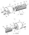
図5は、照明装置200の外観を示す分解斜視図である。照明装置200は、直管形LEDランプ100と、直管形LEDランプ100を装着する照明器具(灯具)150とを備えている。
照明器具150は、蛍光灯を点灯させるための器具と同じものであり、ソケット151a、151bの穴位置に合わせて直管形LEDランプ100の端子(4a〜4d)を差し込む。
商業用電流が端子(4a〜4d)から直管形LEDランプ100内の後述するLED素子に流れ、直管形LEDランプ100が点灯するようになっている。
Hereinafter, an embodiment of the present invention will be described with reference to the drawings.
First, based on FIG. 5 thru | or FIG. 10, the basic structure of the straight tube | pipe type LED lamp as an LED lamp which concerns on this embodiment, and an illuminating device is demonstrated.
FIG. 5 is an exploded perspective view showing the appearance of the
The
The commercial current flows from the terminals (4a to 4d) to the LED elements described later in the straight
直管形LEDランプ100は、主に、棒状(平板状、筒状の概念を含む)の筐体2と、透光性で且つ拡散性のカバー部材としてのカバー3と、照明器具150に電気的に接続可能な口金1a、1bとから構成されている。
ここでは、カバー3は透明のものを用いている。カバー3の拡散性は、カバー表面にプリズム状の凹凸を付加するなどして形状的に付与してもよく、拡散材料を含むことにより付与してもよい。
拡散材料を含む場合には、拡散材料でカバー3全体を形成してもよく、拡散材料を添加ないし含有させて拡散性を付与してもよい。
The straight
Here, the
When the diffusion material is included, the
筐体2は、断面形状が長手方向(軸方向)全体に亘って略同一の半円筒状(筒状)に形成されている。
内部で生じる熱の放熱機能を向上させるために、筐体2の外面には凹凸が付与され(図10参照)、表面積を大きくしている。
筐体2は、熱伝導率の大きい金属材料で形成されている。筒形状であるために、押出し成形や引き抜き成形等の加工方法により、断面形状が均一な筐体2を安価に製作できる。
The
In order to improve the function of radiating heat generated inside, the outer surface of the
The housing | casing 2 is formed with the metal material with large heat conductivity. Due to the cylindrical shape, the
金属材料としては、アルミニウム合金やマグネシウム合金が多く用いられるが、他の押出し材料等でも良い。
外周部の凹凸により、リブや放熱フィンを設けるのと同じような放熱機能を持たせることができる。
ここでは放熱性向上を目的として、筐体2の外周部に凹凸を設けるようにしているが、筐体2と後述する駆動基板(電源基板)や電気部品との絶縁性が確保できれば内周部に凹凸を設けても良い。
As the metal material, an aluminum alloy or a magnesium alloy is often used, but other extruded materials may be used.
The unevenness of the outer peripheral portion can provide a heat dissipation function similar to that provided with ribs or heat dissipation fins.
Here, for the purpose of improving heat dissipation, the outer periphery of the
カバー3は、筐体2の外径とほぼ同じ外径(曲率)を有し、筐体2の長手方向に沿う開口部を有する半円形状に形成されている。
すなわち、カバー3は円弧状の断面形状を有し、筐体2の一側面を長手方向に亘って覆う大きさを有している。
カバー3は、図10に示すように、筐体2の外面に設けた軸方向に延びる溝21に、端縁33を嵌め込む形で取り付けられ、筐体2との一体構成は円筒形状となる。
図5に示すように、口金1a、1bは、筐体2とカバー3との一体構成であるランプ本体の長手方向両端部にその外面を覆うように設けられている。
口金1a、1bには、図8に示すように、蛍光灯を点灯可能な照明器具(蛍光灯照明器具)150に搭載可能な端子4a〜4dが装備されている。
The
That is, the
As shown in FIG. 10, the
As shown in FIG. 5, the
As shown in FIG. 8, the
口金1a、1bの端子4a〜4dと、口金1a、1bに接続されたコネクタ16から延びるリ−ド線6a、6bを介して電源基板7に電流が供給される。
端子4a〜4dと、リ−ド線6a、6bとを直接はんだ付けなどの方法で電気的に接続しても問題はない。
口金1a、1bは、複数のねじ5a〜5dによって筐体2に固定されることで、筐体2とこれに嵌合されたカバー3とが一体になるように包み込んでいる。
Current is supplied to the
There is no problem even if the
The
口金1a、1bは、ねじ止めではなく、筐体2にカシメ等の手段により固定してもよい。口金1a、1bの形状は、既存の蛍光灯の両端部に位置する口金と略同一の形状となっている。
したがって、蛍光灯が用いられている既存の照明器具に対して、直管形LEDランプ100を蛍光灯に代えて取り付けることにより、照明器具の交換を要することなくLEDランプの照明装置を構成することができる。
これにより、別途新たな照明器具を取り付ける場合に比べて、設備コストや工事コストを大幅に低減できるとともに、交換作業の労力の低減、時間短縮を実現できる。
The
Therefore, an LED lamp illumination device can be configured without requiring replacement of the luminaire by attaching the straight
Thereby, compared with the case where a new lighting fixture is separately attached, the facility cost and the construction cost can be greatly reduced, and the labor and time for replacement work can be reduced.
図10に示すように、筐体2の平坦部(半円形の弦に相当する部分)32の外側であってカバー3の内方には、カバー3に対向して、実装基板としてのLED基板11が粘着性を有するシート10を介して固定(支持)されている。
シート10は、LEDで発生する熱を筐体2に伝え易くするために、すなわち放熱を促進させるために、熱伝導性のよい材質(例えば放熱シリコ−ンゴム等)が望ましい。
電源基板7は、平坦部32の内側に沿うように、筐体2の内部に配置されている。
図6に示すように、LED基板11は細長い長方形状のプリント基板であり、LED基板11aとLED基板11bとから構成されている。
As shown in FIG. 10, an LED substrate as a mounting substrate that faces the
The
The
As shown in FIG. 6, the
LED基板11の分割構成に対応して、シート10も長手方向に分割されている。
LED基板11a、11bにはそれぞれ、LED素子12a、12bが筐体2の長手方向に所定の間隔で複数実装されている。
LED素子12は、EL(Electro Luminescence)効果を持つ半導体発光素子光源である。
Corresponding to the divided configuration of the
A plurality of
The
図7に示すように、電源基板7は筐体2の長手方向に延びる細長い長方形状に形成されており、その実装面には直流電源変換用の電子部品9が長手方向に間隔をおいて複数搭載されている。
As shown in FIG. 7, the
電子部品9によって直流に整流された電流は、図9(a)に示すリード線13a、13bを通して実装基板11a、11bに供給される。
LED基板11a、11bの間は、図示しないリード線やジャンパー線などで電気的に接続されている。
本実施形態では半導体発光素子を実装する実装基板(LED基板)を2枚の直列配置構成としているが、1枚や3枚以上の直列配置構成でもよく、並列構成でもよい。
The current rectified to direct current by the
The
In the present embodiment, the mounting substrate (LED substrate) on which the semiconductor light emitting element is mounted has a two-series arrangement configuration, but one or three or more series arrangement configurations or a parallel configuration may be used.
図1乃至図4に基づいて本発明の一実施形態を説明する。
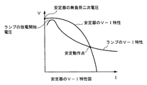
まず、図4に基づいて、インバータ安定器(電子安定器)の出力電圧の変動とちらつきが生じる原理について説明する。
図4は、蛍光灯用のインバータ安定器のV−I特性を示した図である。インバータ安定器はV−I特性に従って出力電圧によって出力電流が決定する。
このため、蛍光灯より低い出力電圧(インピーダンス)の領域、すなわち、図4の安定動作点よりも右側の領域で使用することによって省エネルギー性を高めることができる。しかし、安定動作点よりも低いインピーダンスで使用すると、安定器内のPFC(力率改善)動作が不安定になり、出力電圧が大幅に変動するインバータ安定器が存在する。
An embodiment of the present invention will be described with reference to FIGS.
First, based on FIG. 4, the principle of fluctuation and flickering of the output voltage of the inverter ballast (electronic ballast) will be described.
FIG. 4 is a diagram showing VI characteristics of an inverter ballast for a fluorescent lamp. In the inverter ballast, the output current is determined by the output voltage according to the VI characteristic.
For this reason, energy saving can be improved by using in the area | region of the output voltage (impedance) lower than a fluorescent lamp, ie, the area | region of the right side rather than the stable operating point of FIG. However, when used at an impedance lower than the stable operating point, the PFC (power factor correction) operation in the ballast becomes unstable, and there is an inverter ballast in which the output voltage varies greatly.
インバータ安定器への接続時のインピーダンス制御では、蛍光灯用のインバータ安定器の省エネルギー性を高めるために、インピーダンスを可変させて有効電力を低減させていく。有効電力を低減させていくと、インバータ安定器内のPFC回路のスイッチング素子のON幅が極小となり、PFC動作が不安定になる。PFC動作が不安定になることでインバータ安定器の出力電圧が変動し、LED素子に対して入力変動が生じる。この入力変動が原因でLEDのちらつきとして現れる。 In the impedance control at the time of connection to the inverter ballast, the impedance is varied to reduce the effective power in order to improve the energy saving property of the inverter ballast for the fluorescent lamp. When the active power is reduced, the ON width of the switching element of the PFC circuit in the inverter stabilizer becomes minimum, and the PFC operation becomes unstable. When the PFC operation becomes unstable, the output voltage of the inverter ballast fluctuates, and the input fluctuation occurs with respect to the LED element. Appearing as LED flicker due to this input fluctuation.
インバータ安定器内のPFC動作が不安定になると、インバータ安定器の出力電圧の変動が大幅に上がる特徴がある。
本発明では、インバータ安定器の二次電圧の振幅をLED素子12に流れる電流の脈流として検出する。インピーダンス制御における次の制御とその前の制御との脈流の振幅差が所定値を超えた場合にはインバータ安定器の出力電圧が不安定になったと判断する。その場合、不安定になる前の制御値(インピーダンス値)に戻す制御を行うことによってちらつきを抑制する。以下にその構成を説明する。
When the PFC operation in the inverter ballast becomes unstable, the output voltage fluctuation of the inverter ballast is greatly increased.
In the present invention, the amplitude of the secondary voltage of the inverter ballast is detected as a pulsating current flowing in the
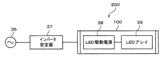
図1は、照明装置200の概略ブロック図である。照明装置200は、照明器具150に外から見えない状態に配置され、商用電源36に接続されるインバータ安定器37と、インバータ安定器37に接続される直管形LEDランプ100とを有している。
直管形LEDランプ100は、LED駆動電源(LED駆動回路)38と、LED素子12群からなるLEDアレイ39とを有している。
FIG. 1 is a schematic block diagram of the
The straight
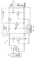
本実施形態におけるインピーダンス制御用回路の構成を図2に示す。
整流回路としてのダイオードブリッジ40は、インバータ安定器37からのAC(交流)電力を全波整流してダイオードブリッジ後をDC(直流)化する。
入力平滑コンデンサC1は、全波整流された電力の平滑化をするもので、制御用トランジスタQ1でその挿入のON/OFFが制御される。
スイッチング平滑コンデンサC2は、スイッチングされた電力の平滑化をするもので、制御用トランジスタQ2でその挿入のON/OFFが制御される。
符号L1はスイッチング用インダクタを、D1はスイッチング用ダイオードを示している。
The configuration of the impedance control circuit in this embodiment is shown in FIG.
The
The input smoothing capacitor C1 smoothes full-wave rectified power, and ON / OFF of the insertion is controlled by the control transistor Q1.
The switching smoothing capacitor C2 smoothes the switched electric power, and ON / OFF of the insertion is controlled by the control transistor Q2.
Reference numeral L1 denotes a switching inductor, and D1 denotes a switching diode.
符号Q3はスイッチング用インダクタL1のバイパス制御用トランジスタを示している。バイパス制御用トランジスタQ3は、スイッチング用インダクタL1の両端に並列に接続され、バイパス時にはONしてスイッチング用インダクタL1をショート状態にし、バイパスOFF時にはOFFしてスイッチング用インダクタL1を有効にする。
符号Q4はスイッチング素子を示している。スイッチング素子Q4のスイッチングにより、LED素子12に流れるLED電流をPWM(Pulse Width Modulation)制御する。
Reference sign Q3 indicates a bypass control transistor of the switching inductor L1. The bypass control transistor Q3 is connected in parallel to both ends of the switching inductor L1, and is turned on when bypassing to short-circuit the switching inductor L1, and is turned off when bypass is OFF to enable the switching inductor L1.
Reference sign Q4 indicates a switching element. The LED current flowing through the
符号R1はLED電流検出抵抗を示している。電流値×抵抗値の電圧を制御手段としてのマイクロコンピュータ41のA/Dコンバータで読み取って、電流値を算出する。マイクロコンピュータ41は回路全体の制御を行うものである。
マイクロコンピュータ41は、後述する点灯条件を保持する不揮発性メモリとしてのEEPROM(Electrically Erasable Programmable ROM)42と、LED素子12に流れるLED電流の脈流を検出する出力状態検出手段としてのADC(Analog to Digital Converter)端子43を備えている。
Reference symbol R1 indicates an LED current detection resistor. The current value × resistance value voltage is read by the A / D converter of the microcomputer 41 as the control means to calculate the current value. The microcomputer 41 controls the entire circuit.
The microcomputer 41 includes an EEPROM (Electrically Erasable Programmable ROM) 42 as a non-volatile memory that holds lighting conditions to be described later, and an ADC (Analog to Analog) as an output state detection unit that detects a pulsating flow of the LED current flowing through the
大まかな動作原理は以下の通りである。
(1)点灯時には制御用トランジスタQ1、Q2はOFF、スイッチング用インダクタL1はバイパス制御用トランジスタQ3によりバイパスされている。点灯時にC(コンデンサ)やL(インダクタ)の負荷があると点灯しない場合があるためである。
(2)点灯後制御用トランジスタQ1、Q2をONし、スイッチング用インダクタL1をバイパスしているバイパス制御用トランジスタQ3をOFFする。
(3)制御用トランジスタQ1、Q2のONと、バイパス制御用トランジスタQ3のOFFのタイミングは、制御用トランジスタQ1、Q2をONしてから一定時間経過後(例えば2秒後)にバイパス制御用トランジスタQ3をOFFする。
The general operation principle is as follows.
(1) At the time of lighting, the control transistors Q1 and Q2 are OFF, and the switching inductor L1 is bypassed by the bypass control transistor Q3. This is because if there is a load of C (capacitor) or L (inductor) at the time of lighting, it may not light up.
(2) After the lighting, the control transistors Q1 and Q2 are turned on, and the bypass control transistor Q3 bypassing the switching inductor L1 is turned off.
(3) The ON timing of the control transistors Q1 and Q2 and the OFF timing of the bypass control transistor Q3 are the bypass control transistors after a lapse of a certain time (eg, 2 seconds) after the control transistors Q1 and Q2 are turned ON. Turn off Q3.
(4)PWM制御により、定められた狙いのLED電流となるように制御を行う。PWM制御はスイッチング素子Q4のオンDutyを0%から、狙いのLED電流になるまで増大させる。PWM制御はオンDuty0%からスタートし、Dutyを上げていく。例えば1秒毎に5%Duty上げる。オンDutyが上がるとLED電流は下がって行く。狙いのLED電流値まで下がったときのDutyを点灯条件とする。
(4) By PWM control, control is performed so as to achieve a predetermined target LED current. The PWM control increases the ON duty of the switching element Q4 from 0% until the target LED current is reached. The PWM control starts from on
本発明では、上記(4)の制御中にインバータ安定器37の出力が不安定になった場合、それをADC端子43で検出し、インバータ安定器37の出力が安定するDutyで点灯させることを目的とする。
インバータ安定器の種類によっては、あるオンDutyまで上げると安定器の出力電圧が大幅に変動し、この変動に起因してLEDがちらつく。LEDのちらつきはLED電流の脈流として現れる。
LED電流の脈流を制御回路内のADC端子43で監視する。設定したスレッシュ値(所定値)を超えた場合、インバータ安定器37の出力が不安定になったと判断し、不安定になる前のDutyへ戻すことでインバータ安定器37の出力不安定を解消することが可能になる。
In the present invention, when the output of the
Depending on the type of inverter ballast, the output voltage of the ballast greatly fluctuates when it is raised to a certain on-duty, and the LED flickers due to this fluctuation. LED flickering appears as a pulsating flow of LED current.
The LED current pulsation is monitored at the
図3は脈流検出の概念を示す図である。インピーダンス制御におけるLED電流の脈流は、ADC端子43で監視される。例えば、Duty55%のLED電流では脈流の振幅はm1であり、Dutyを1STEP下げると、Duty50%のLED電流では脈流の振幅はm2となる。
マイクロコンピュータ41は、Duty55%時の脈流の振幅m1と、Duty50%時の脈流の振幅m2とを比較し、
(m2−m1)>スレッシュ値
の場合には、インバータ安定器37の出力電圧が不安定になったと判断する。
FIG. 3 is a diagram showing the concept of pulsating flow detection. The pulsating flow of the LED current in the impedance control is monitored at the
The microcomputer 41 compares the amplitude m1 of the pulsating flow when the duty is 55% with the amplitude m2 of the pulsating flow when the duty is 50%,
If (m2-m1)> the threshold value, it is determined that the output voltage of the
インバータ安定器37の出力電圧が不安定になったと判断した場合には、インバータ安定器37の出力電圧が安定する領域で点灯する制御を行う。すなわち、破線矢印で示すように、Dutyをインバータ安定器37の出力電圧が安定していたインピーダンス値(Duty55%)に戻す制御を行う。
When it is determined that the output voltage of the
上記のように、本発明では、LED制御の回路上にマイクロコンピュータ41を設け、あるインピーダンス値でのインバータ安定器の出力変動をマイクロコンピュータ41のADC端子43でLED電流の脈流として検出する。このため、検出時にインバータ安定器の出力電圧の安定するインピーダンス値まで戻すことが可能になる。
本発明によれば、電子安定器の出力電圧が不安定になったことによってちらつきが生じていることを迅速に把握でき、ちらつきを抑制する対策を自動的に、あるいは手動操作により講じることができる。
As described above, in the present invention, the microcomputer 41 is provided on the LED control circuit, and the output fluctuation of the inverter stabilizer at a certain impedance value is detected at the
According to the present invention, it is possible to quickly grasp that flickering is caused by the output voltage of the electronic ballast becoming unstable, and it is possible to take measures to suppress flickering automatically or manually. .
さて、上述の実施形態においては、インバータ安定器37の出力状態を、LED電流の脈流を検知することで判断したが、インバータ安定器37の出力電圧が不安定になったときには、実際には設計によって異なる様々な波形を出力する場合が考えられる。
具体的には例えば、図11(a)に示すように、出力電流が極端に減少するような場合や、図11(b)に示すように、出力が瞬断してしまう場合などが考えられる。
そこで、本実施形態では、かかる出力状態の不安定を、マイクロコンピュータ41を用いて検知する。
In the above embodiment, the output state of the
Specifically, for example, as shown in FIG. 11 (a), the output current may be extremely reduced, or the output may be momentarily interrupted as shown in FIG. 11 (b). .
Therefore, in this embodiment, such an output state instability is detected using the microcomputer 41.
なお、以降の説明において特に必要のあるときには、図2を用いて既に示したインピーダンス制御用回路を制御回路50として説明する。
Note that the impedance control circuit already shown in FIG. 2 will be described as the
まず、図11(a)に示すように、キャリブレーション中に極端にインバータ安定器37からの電流が減少するときの制御回路50の動作について説明する。
なお、「極端に」電流が減少するとは例えばLED電流が、一点鎖線で図中に電流値I1で示した所定の動作電流値よりも20mA以上低い電流値となった場合を示している。しかしながら、かかる構成に限定されるものではなく、かかる20mAの数値は設計値によって種々の値をとって良い。
First, as shown in FIG. 11A, the operation of the
Incidentally, "extremely", for example LED current and current decreases, it shows a case where a current value lower than 20mA than a predetermined operating current value indicated by the current value I 1 in the figure by the dashed line. However, the present invention is not limited to such a configuration, and the numerical value of 20 mA may take various values depending on design values.
ADC端子43は、すでに述べたように、LED電流検出抵抗R1を用いて、出力電圧あるいは出力電流を監視している。
マイクロコンピュータ41は、PWM制御によってスイッチング素子Q4のオンDutyを0%から1秒ごとに5%刻みで上昇させる。なお、ここでQ4のオンDutyを上げる(=オフDutyを下げる)ことは、制御回路50のインピーダンスが下がることを意味する。このように制御回路50のインピーダンス制御により、インバータ安定器37の出力電流が減少することでLED電流が減少する。なお、かかるスイッチング素子Q4のオンDutyの変化量および変化の1STEPごとの時間については、任意に設定して良く、例えば100ms毎に3.125%ずつDutyを上昇させるとしても良い。
As described above, the
The microcomputer 41 raises the on-duty of the switching element Q4 from 0% in increments of 5% every second by PWM control. Here, increasing the on-duty of Q4 (= lowering off-duty) means that the impedance of the
さて、図11(a)に示すような状況は例えば、インピーダンス制御を行うとき、インバータ安定器37側が「所定の出力電流が出ない」と判断して保護回路が働いてLED電流を極端に抑制するような場合が挙げられる。
ADC端子43は、所定の、あるいは設計された電流値I1よりも極端に電流が低くなったことを検知すると、かかる電流値を計測した時点のDutyたる第1のDutyD1をマイクロコンピュータ41に記憶する。ADC端子43は、一端キャリブレーション操作を中断して、再度Duty0%から5%刻みでスイッチング素子Q4のオンDutyを上昇させる。
なお、ここで一度オンDuty0%に戻す理由は、インバータ安定器37側にある保護回路の保護動作をリセットするためであり、インバータ安定器37側の設計による。
In the situation shown in FIG. 11A, for example, when the impedance control is performed, the
Note that the reason why the duty ratio is once returned to
本実施形態では、マイクロコンピュータ41は、記憶された第1のDutyD1があるときには、当該第1のDutyよりも大きいDutyであって、インバータ安定器37の出力電圧が安定するDutyで点灯する制御を行う。
かかる構成により、インバータ安定器37側の保護回路が動作するような構成であっても、スイッチング素子Q4のDutyの調整によって、最適な出力電流値が確保される。すなわち、かかる構成により、電子安定器の保護動作による出力電圧の不安定化を迅速に把握し、抑制することができる。
In the present embodiment, when there is a stored first duty D1, the microcomputer 41 controls to turn on at a duty that is larger than the first duty and at which the output voltage of the
With this configuration, even when the protection circuit on the
以上述べたように、本実施形態では、出力状態検出手段たるADC端子43が、インバータ安定器37の出力変動を、LED素子21に流れる電流のDuty比から検出する。
かかる構成により、電子安定器の保護動作による出力電圧の不安定化を迅速に把握し、抑制することができる。
As described above, in the present embodiment, the
With this configuration, it is possible to quickly grasp and suppress the output voltage instability due to the protection operation of the electronic ballast.
次に、図11(b)に示すように、所定のDutyD1以下の数値において、インバータ安定器37の保護回路が動作した時に、出力電圧がゼロになる、言い換えるとインバータ安定器37が出力を停止するような場合について説明する。
このようにインバータ安定器37が出力を停止してしまうと、マイクロコンピュータ41にも電流が流れなくなってしまうため、ADC端子43が電流を検知することができなくなり、キャリブレーションができない。
Next, as shown in FIG. 11B, the output voltage becomes zero when the protection circuit of the
When the
そこで、本実施形態では、制御回路50は、インバータ安定器37が出力を停止したことを検知する停止検知手段としてのEEPROM42を有している。
制御回路50は、図12に示すような点灯方法の制御フローに従って、インバータ安定器37が保護回路によって出力を停止してしまうような場合であってもちらつきの発生を迅速に把握し、抑制するように制御する。
Therefore, in the present embodiment, the
The
まず、LEDランプ100の点灯時において、マイクロコンピュータ41は、PWM制御によってスイッチング素子Q4のオンDutyを0%から1秒ごとに5%刻みで上昇させる(ステップS101)。
マイクロコンピュータ41は、インバータ安定器37が出力を停止していないかどうかをADC端子43を用いて監視する(ステップS102)。
インバータ安定器37側の保護回路が動作して、インバータ安定器37が出力を停止すると、マイクロコンピュータ41は、不揮発性メモリであるEEPROM42を用いて、消灯条件すなわちインバータ安定器37が停止した第1のDutyであるDutyD1を記憶する(ステップS104)。
なお、ここでインバータ安定器37が出力を停止することなく、LED電流が最適値あるいは所定の電流値になったときには、キャリブレーション操作を終了して、当該電流値でLEDランプ100を点灯させる(ステップS103)。
ステップS104において、DutyD1が記憶されると、ADC端子43は、一端キャリブレーション操作を中断して、再度Duty0%から5%刻みでスイッチング素子Q4のオンDutyを上昇させる(ステップS105)。
First, when the
The microcomputer 41 uses the
When the
Here, when the LED current reaches an optimum value or a predetermined current value without stopping the output of the
In step S104, when DutyD1 is stored, the
インバータ安定器37側の保護回路が再度動作して、インバータ安定器37が出力を停止すると、マイクロコンピュータ41は、ステップS104と同様に、EEPROM42を用いて、消灯条件すなわちインバータ安定器37が停止した第2のDutyであるDutyD2を記憶する(ステップS106)。
なお、ここでインバータ安定器37が出力を停止することなく、LED電流が最適値あるいは所定の電流値になったときには、キャリブレーション操作を終了して、当該電流値でLEDランプ100を点灯させる(ステップS103)。
When the protection circuit on the
Here, when the LED current reaches an optimum value or a predetermined current value without stopping the output of the
本実施形態では、キャリブレーション中にインバータ安定器37が出力を停止したことを条件として、EEPROM42が、出力が停止したときのスイッチング素子Q4のDutyを第2のDutyD2として記憶する(ステップS107)。
この点についてさらに詳しく説明する。
キャリブレーション中にインバータ安定器37が出力を停止する状態とは、インバータ安定器37の保護回路が動作した場合に加えて、例えば点灯直後に使用者がスイッチを切る操作をする場合など、様々な状態が考えられる。
しかしながら、特にインバータ安定器37の保護回路が動作した場合には、ある決まったLED電流において保護回路が動作するはずである。
In the present embodiment, on condition that the
This point will be described in more detail.
The state where the
However, especially when the protection circuit of the
そこで本実施形態では、キャリブレーション中にインバータ安定器37が出力停止状態となったことを条件として、EEPROM42を用いて第1のDutyD1および第2のDutyD2を記憶する。
さらに、マイクロコンピュータ41は、第1のDutyD1と第2のDutyD2とを比較し、近似あるいは同一の値とみなせる程度の差しかない場合には、かかる出力停止を、インバータ安定器37の保護回路が動作したためであると判断する(ステップS108)。
具体的には、第1のDutyD1と第2のDutyD2との間の差が±5%以内であった場合に、マイクロコンピュータ41は、インバータ安定器37の出力停止を、保護回路の動作によるものと判断する。なお、かかる構成に限定されるものではなく、近似あるいは同一の値とみなせる程度の差であれば、5%に限るものではない。
Therefore, in the present embodiment, the first duty D1 and the second duty D2 are stored using the
Further, the microcomputer 41 compares the first duty D1 and the second duty D2, and if there is no difference between the two values that can be regarded as approximate or the same value, the protection circuit of the
Specifically, when the difference between the first duty D1 and the second duty D2 is within ± 5%, the microcomputer 41 stops the output of the
なお、ステップS108において、第1のDutyD1と第2のDutyD2とが大きく離れている場合には、何れかの出力停止が、例えば使用者の操作などによるものであると判断して、再びインバータ安定器37が出力を停止するまで監視を続ける。
またステップS108において、D1=D2またはD1≒D2と判断された場合には、DutyD1とDutyD2とを比較して、何れか小さい方よりも小さい第3のDutyD3にスイッチング素子Q4のDutyを設定する(ステップS109)。
In step S108, if the first duty D1 and the second duty D2 are far apart, it is determined that one of the output stops is caused by, for example, a user operation, and the inverter is stabilized again. Monitoring continues until the
If it is determined in step S108 that D1 = D2 or D1≈D2, the duty D1 is compared with the duty D2, and the duty of the switching element Q4 is set to the third duty D3 smaller than the smaller one (see FIG. Step S109).
このように、制御回路50は、インバータ安定器37の出力電圧が安定するDutyで点灯するように制御を行う制御手段としての機能を有している。
かかる構成により、電子安定器の保護動作による出力電圧の不安定化を迅速に把握し、抑制することができる。
As described above, the
With this configuration, it is possible to quickly grasp and suppress the output voltage instability due to the protection operation of the electronic ballast.
本実施形態では、マイクロコンピュータ41は、インバータ安定器37の出力が停止したことを検知するEEPROM42を有している。
かかる構成により、インバータ安定器37が出力を停止したときにも、電子安定器の保護動作による出力電圧の不安定化を迅速に把握し、抑制することができる。
In the present embodiment, the microcomputer 41 has an
With such a configuration, even when the
本実施形態では、制御回路50は、インバータ安定器37の出力が停止した第1のDutyD1と、第1のDutyD1よりも後にインバータ安定器37の出力が停止した第2のDutyD2と、を記憶している。
また、第1のDutyD1と第2のDutyD2との差が所定値以内であることを条件として、制御回路50が設定するDutyを前記第1のDutyと前記第2のDutyとの何れか小さい方よりも小さい値に設定する。
かかる構成により、インバータ安定器37が出力を停止したときにも、電子安定器の保護動作による出力電圧の不安定化を迅速に把握し、抑制することができる。
In the present embodiment, the
Also, on condition that the difference between the first duty D1 and the second duty D2 is within a predetermined value, the duty set by the
With such a configuration, even when the
本実施形態では、LEDランプ100は、インバータ安定器37への接続時、インピーダンスを可変させてインバータ安定器37の出力電流を狙いの電流値に制御するインピーダンス制御を行い、インバータ安定器37の出力が停止したことを検出し、インバータ安定器37の出力が停止したことが検出されたことを条件として、インバータ安定器37の出力電圧が安定するDutyで点灯する。
かかる構成により、インバータ安定器37が出力を停止したときにも、電子安定器の保護動作による出力電圧の不安定化を迅速に把握し、抑制することができる。
In the present embodiment, when connected to the
With such a configuration, even when the
以上、本発明の好ましい実施の形態について説明したが、本発明はかかる特定の実施形態に限定されるものではなく、上述の説明で特に限定しない限り、特許請求の範囲に記載された本発明の趣旨の範囲内において、種々の変形・変更が可能である。
本発明の実施の形態に記載された効果は、本発明から生じる最も好適な効果を例示したに過ぎず、本発明による効果は、本発明の実施の形態に記載されたものに限定されるものではない。
The preferred embodiments of the present invention have been described above. However, the present invention is not limited to such specific embodiments, and unless specifically limited by the above description, the present invention described in the claims is not limited. Various modifications and changes are possible within the scope of the gist.
The effects described in the embodiments of the present invention are merely examples of the most preferable effects resulting from the present invention, and the effects of the present invention are limited to those described in the embodiments of the present invention. is not.
12 LED素子
37 電子安定器(インバータ安定器)
41 制御手段(マイクロコンピュータ)
42 停止検知手段(EEPROM)
43 出力状態検出手段(ADC端子)
100 LEDランプ
150 照明器具
200 照明装置
D1 第1のDuty
D2 第2のDuty
12
41 Control means (microcomputer)
42 Stop detection means (EEPROM)
43 Output state detection means (ADC terminal)
DESCRIPTION OF
D2 Second Duty
Claims (12)
前記電子安定器の出力電圧が不安定になったことを検出する出力状態検出手段を有するLEDランプ。 An LED lamp comprising an LED element and connectable to an electronic ballast for a fluorescent lamp,
An LED lamp having output state detecting means for detecting that the output voltage of the electronic ballast has become unstable.
前記出力状態検出手段により前記電子安定器の出力電圧が不安定になったことが検出されたとき、前記電子安定器の出力電圧が安定する領域で点灯する制御を行う制御手段を有するLEDランプ。 The LED lamp according to claim 1, wherein
The LED lamp which has a control means which controls to light in the area | region where the output voltage of the said electronic ballast is stabilized, when it is detected by the said output state detection means that the output voltage of the said electronic ballast became unstable.
前記出力状態検出手段が、前記電子安定器の出力変動を前記LED素子に流れる電流の脈流として検出するLEDランプ。 The LED lamp according to claim 2,
The LED lamp in which the output state detection means detects an output fluctuation of the electronic ballast as a pulsating current flowing in the LED element.
前記制御手段は、インピーダンスを可変させて前記電子安定器の出力電流を狙いの電流値に制御するインピーダンス制御を行い、前記出力状態検出手段で検出される脈流の振幅差が所定値を超えたときは、前記制御手段は前記電子安定器の出力電圧が不安定になったと判断し、インピーダンスを前記電子安定器の出力電圧が不安定になる前の値に戻すLEDランプ。 The LED lamp according to claim 3,
The control means performs impedance control in which the impedance is varied to control the output current of the electronic ballast to a target current value, and the amplitude difference of the pulsating flow detected by the output state detection means exceeds a predetermined value. When the control means determines that the output voltage of the electronic ballast has become unstable, the LED lamp returns the impedance to a value before the output voltage of the electronic ballast becomes unstable.
前記出力状態検出手段が、前記電子安定器の出力変動を、前記LED素子に流れる電流のDuty比から検出することを特徴とするLEDランプ。 The LED lamp according to claim 2 to 4,
The LED lamp, wherein the output state detection means detects an output fluctuation of the electronic ballast from a duty ratio of a current flowing through the LED element.
前記制御手段は、前記電流を狙いの電流値に制御するインピーダンス制御を行い、
前記出力状態検出手段で検出された前記電流が前記狙いの電流値より20mA以上低いことを条件として、前記電子安定器の出力電圧が不安定になったと判断することを特徴とするLEDランプ。 The LED lamp according to claim 5,
The control means performs impedance control for controlling the current to a target current value,
The LED lamp, wherein the output voltage of the electronic ballast is determined to be unstable on the condition that the current detected by the output state detection means is 20 mA or more lower than the target current value.
前記出力状態検出手段は、前記電子安定器の出力が停止したことを検知する停止検知手段を備えたことを特徴とするLEDランプ。 The LED lamp according to any one of claims 1 to 6,
The LED lamp according to claim 1, wherein the output state detection means includes a stop detection means for detecting that the output of the electronic ballast is stopped.
前記停止検知手段により前記電子安定器の出力が停止したことを条件として、
前記電子安定器の出力電圧が安定するDutyで点灯する制御を行う制御手段を有するLEDランプ。 The LED lamp according to claim 7,
On condition that the output of the electronic ballast is stopped by the stop detection means,
The LED lamp which has a control means which controls to light by Duty which the output voltage of the said electronic ballast is stabilized.
前記制御手段は、前記電子安定器の出力が停止した第1のDutyと、前記第1のDutyよりも後に前記電子安定器の出力が停止した第2のDutyと、を記憶し、
前記第1のDutyと前記第2のDutyとの差が所定値以内であることを条件として、前記制御手段が設定するDutyを前記第1のDutyと前記第2のDutyとの何れか小さい方よりも小さい値に設定することを特徴とするLEDランプ。 The LED lamp according to claim 8,
The control means stores a first duty when the output of the electronic ballast is stopped and a second duty when the output of the electronic ballast is stopped after the first duty;
On the condition that the difference between the first duty and the second duty is within a predetermined value, the duty set by the control means is the smaller of the first duty and the second duty An LED lamp characterized by being set to a smaller value.
前記電子安定器への接続時、インピーダンスを可変させて前記電子安定器の出力電流を狙いの電流値に制御するインピーダンス制御を行い、前記電子安定器の出力電圧が不安定になったことを、前記LED素子に流れる電流の脈流を監視することによって検出し、前記電子安定器の出力電圧が不安定になったことが検出された場合、インピーダンスを前記電子安定器の出力電圧が不安定になる前の値に戻して点灯するLEDランプの点灯方法。 An LED lamp lighting method comprising an LED element and connectable to an electronic ballast for a fluorescent lamp,
When connecting to the electronic ballast, impedance control is performed to vary the impedance and control the output current of the electronic ballast to a target current value, and the output voltage of the electronic ballast becomes unstable. Detecting by monitoring the pulsating current flowing through the LED element and detecting that the output voltage of the electronic ballast becomes unstable, the impedance becomes unstable when the output voltage of the electronic ballast is unstable. LED lamp lighting method to return to the previous value and turn on.
前記電子安定器への接続時、インピーダンスを可変させて前記電子安定器の出力電流を狙いの電流値に制御するインピーダンス制御を行い、前記電子安定器の出力が停止したことを検出し、前記電子安定器の出力が停止したことが検出されたことを条件として、前記電子安定器の出力電圧が安定するDutyで点灯するLEDランプの点灯方法。 An LED lamp lighting method comprising an LED element and connectable to an electronic ballast for a fluorescent lamp,
When connecting to the electronic ballast, impedance control is performed to control the output current of the electronic ballast to a target current value by changing impedance, and detecting that the output of the electronic ballast is stopped, the electronic ballast A method for lighting an LED lamp that is lit at a duty at which the output voltage of the electronic ballast is stabilized on the condition that the output of the ballast is stopped.
Applications Claiming Priority (2)
| Application Number | Priority Date | Filing Date | Title |
|---|---|---|---|
| JP2016087333 | 2016-04-25 | ||
| JP2016087333 | 2016-04-25 |
Publications (1)
| Publication Number | Publication Date |
|---|---|
| JP2017199644A true JP2017199644A (en) | 2017-11-02 |
Family
ID=60238085
Family Applications (1)
| Application Number | Title | Priority Date | Filing Date |
|---|---|---|---|
| JP2016190194A Pending JP2017199644A (en) | 2016-04-25 | 2016-09-28 | Led lamp, lighting device and lighting method of led lamp |
Country Status (1)
| Country | Link |
|---|---|
| JP (1) | JP2017199644A (en) |
Cited By (2)
| Publication number | Priority date | Publication date | Assignee | Title |
|---|---|---|---|---|
| WO2020009268A1 (en) * | 2018-07-04 | 2020-01-09 | 주식회사엘디티 | Electronic ballast-compatible light emitting diode driving circuit |
| WO2021051266A1 (en) * | 2019-09-17 | 2021-03-25 | 卡任特照明解决方案有限公司 | Driver for led device, led system, and adaptation method for led device |
-
2016
- 2016-09-28 JP JP2016190194A patent/JP2017199644A/en active Pending
Cited By (2)
| Publication number | Priority date | Publication date | Assignee | Title |
|---|---|---|---|---|
| WO2020009268A1 (en) * | 2018-07-04 | 2020-01-09 | 주식회사엘디티 | Electronic ballast-compatible light emitting diode driving circuit |
| WO2021051266A1 (en) * | 2019-09-17 | 2021-03-25 | 卡任特照明解决方案有限公司 | Driver for led device, led system, and adaptation method for led device |
Similar Documents
| Publication | Publication Date | Title |
|---|---|---|
| US8564219B2 (en) | Circuits and methods for driving light sources | |
| US9560700B2 (en) | Illumination lamp and illumination device configured for rapid-start method | |
| JP5537286B2 (en) | LED lighting device | |
| JP5735728B2 (en) | LED lighting fixtures | |
| JP5828103B2 (en) | LED lighting device and lighting apparatus using the same | |
| US9585209B2 (en) | Lighting apparatus and illuminating fixture with the same | |
| JP5447969B2 (en) | LED lighting device and LED lighting apparatus | |
| JP6811386B2 (en) | Dimmer | |
| US20120126710A1 (en) | Circuits and methods for driving light sources | |
| JP6242222B2 (en) | Lighting device and lighting device | |
| JP5988214B2 (en) | Lighting device and lighting apparatus using the same | |
| JP2017199644A (en) | Led lamp, lighting device and lighting method of led lamp | |
| JP2010218715A (en) | Lighting system | |
| JP2017050063A (en) | Illumination lamp, luminaire and lighting method for illumination lamp | |
| JP2016201276A (en) | Lighting circuit, lighting fixture, and illumination system | |
| CN102413604B (en) | Led lighter and lighting device using the led lighter | |
| JP2017004611A (en) | Illumination lamp, illumination apparatus, lighting control circuit, and drive method for illumination lamp | |
| JP6331023B2 (en) | Lighting device and lighting device | |
| JP2012142295A (en) | Led lighting fixture | |
| JP6492954B2 (en) | Lighting lamp, lighting device and lighting control circuit | |
| JP6919294B2 (en) | Light source lighting device | |
| JP2012048998A (en) | Power supply for lighting | |
| JP2013201010A (en) | Illuminating device | |
| JP2017199468A (en) | Led lamp, illumination device, and circuit switching method for led lamp | |
| JP6361330B2 (en) | Light source unit and lighting apparatus |