JP2017197389A - Method for manufacturing semiconductor ceramic composition, semiconductor ceramic composition, and ptc element - Google Patents
Method for manufacturing semiconductor ceramic composition, semiconductor ceramic composition, and ptc element Download PDFInfo
- Publication number
- JP2017197389A JP2017197389A JP2014183887A JP2014183887A JP2017197389A JP 2017197389 A JP2017197389 A JP 2017197389A JP 2014183887 A JP2014183887 A JP 2014183887A JP 2014183887 A JP2014183887 A JP 2014183887A JP 2017197389 A JP2017197389 A JP 2017197389A
- Authority
- JP
- Japan
- Prior art keywords
- temperature
- semiconductor ceramic
- ceramic composition
- composition
- raw material
- Prior art date
- Legal status (The legal status is an assumption and is not a legal conclusion. Google has not performed a legal analysis and makes no representation as to the accuracy of the status listed.)
- Pending
Links
Images


Classifications
-
- C—CHEMISTRY; METALLURGY
- C04—CEMENTS; CONCRETE; ARTIFICIAL STONE; CERAMICS; REFRACTORIES
- C04B—LIME, MAGNESIA; SLAG; CEMENTS; COMPOSITIONS THEREOF, e.g. MORTARS, CONCRETE OR LIKE BUILDING MATERIALS; ARTIFICIAL STONE; CERAMICS; REFRACTORIES; TREATMENT OF NATURAL STONE
- C04B35/00—Shaped ceramic products characterised by their composition; Ceramics compositions; Processing powders of inorganic compounds preparatory to the manufacturing of ceramic products
- C04B35/01—Shaped ceramic products characterised by their composition; Ceramics compositions; Processing powders of inorganic compounds preparatory to the manufacturing of ceramic products based on oxide ceramics
- C04B35/46—Shaped ceramic products characterised by their composition; Ceramics compositions; Processing powders of inorganic compounds preparatory to the manufacturing of ceramic products based on oxide ceramics based on titanium oxides or titanates
- C04B35/462—Shaped ceramic products characterised by their composition; Ceramics compositions; Processing powders of inorganic compounds preparatory to the manufacturing of ceramic products based on oxide ceramics based on titanium oxides or titanates based on titanates
- C04B35/465—Shaped ceramic products characterised by their composition; Ceramics compositions; Processing powders of inorganic compounds preparatory to the manufacturing of ceramic products based on oxide ceramics based on titanium oxides or titanates based on titanates based on alkaline earth metal titanates
- C04B35/468—Shaped ceramic products characterised by their composition; Ceramics compositions; Processing powders of inorganic compounds preparatory to the manufacturing of ceramic products based on oxide ceramics based on titanium oxides or titanates based on titanates based on alkaline earth metal titanates based on barium titanates
-
- H—ELECTRICITY
- H01—ELECTRIC ELEMENTS
- H01C—RESISTORS
- H01C7/00—Non-adjustable resistors formed as one or more layers or coatings; Non-adjustable resistors made from powdered conducting material or powdered semi-conducting material with or without insulating material
- H01C7/02—Non-adjustable resistors formed as one or more layers or coatings; Non-adjustable resistors made from powdered conducting material or powdered semi-conducting material with or without insulating material having positive temperature coefficient
Abstract
Description
この発明は、PTCヒータ、PTCサーミスタ、PTCスイッチ、温度検知器などに用いられる、半導体磁器組成物の製造方法、半導体磁器組成物、その半導体磁器組成物に電極を形成したPTC素子に関する。 The present invention relates to a method for producing a semiconductor ceramic composition used for a PTC heater, a PTC thermistor, a PTC switch, a temperature detector, and the like, a semiconductor ceramic composition, and a PTC element having electrodes formed on the semiconductor ceramic composition.
従来より、PTC(Positive Temperature Coefficient of resistivity)特性を示す材料として、BaTiO3系酸化物に様々な半導体化元素を加えた半導体磁器組成物が提案されている。この半導体磁器組成物に電極を設けたものは、PTC素子として使用することができる。 Conventionally, as a material exhibiting PTC (Positive Temperature Coefficient of Reactive) characteristics, semiconductor porcelain compositions in which various semiconducting elements are added to a BaTiO 3 oxide have been proposed. This semiconductor ceramic composition provided with electrodes can be used as a PTC element.
BaTiO3系酸化物の半導体磁器組成物は、そのキュリー温度が120℃前後であるものが殆どである。これらの半導体磁器組成物は、用途に応じてキュリー温度をシフトさせることが必要になる。例えば、BaTiO3系酸化物にSrTiO3系酸化物を添加することによってキュリー温度をシフトさせることが提案されているが、この場合、キュリー温度は負の方向にのみシフトし、正の方向にはシフトしない。現在実用化されている材料で、キュリー温度を正の方向にシフトさせる添加物として知られているのはPbTiO3である。しかし、鉛は環境汚染を引き起こす元素であるため、鉛を含まない非鉛の半導体磁器組成物が要望されている。 Most BaTiO 3 -based semiconductor ceramic compositions have a Curie temperature of around 120 ° C. These semiconductor porcelain compositions need to shift the Curie temperature depending on the application. For example, it has been proposed to shift the Curie temperature by adding SrTiO 3 oxide to BaTiO 3 oxide, but in this case, the Curie temperature is shifted only in the negative direction and in the positive direction. Do not shift. PbTiO 3 is a material that is currently in practical use and is known as an additive that shifts the Curie temperature in the positive direction. However, since lead is an element that causes environmental pollution, a lead-free semiconductor ceramic composition containing no lead is desired.
非鉛でキュリー温度が高い半導体磁器組成物として、BaTiO3系酸化物におけるBaの一部をBi-Naで置換したものが知られている。
例えば特許文献1は、組成式が[(BiA)x(Ba1-yRy)1-x][Ti1-zMz]O3(AはNa,Li,Kのうち少なくとも一種、RはYを含む希土類元素のうち少なくとも一種、MはNb、Ta、Sbのうち少なくとも一種)で表わされ、x、y、zが、0<x≦0.2、0≦y≦0.02、0≦z≦0.01(但し、y+z>0)を満足する結晶粒を有する半導体磁器組成物が記載されている。
また特許文献1は、その製造方法として、(BiA)TiO3系の第1の原料と(BaR)[TiM]O3(RはYを含む希土類元素のうち少なくとも一種、MはNb、Ta、Sbのうち少なくとも一種であり、R,Mは少なくともどちらか一方が必須である)系の第2の原料をそれぞれ用意し、前記第1の原料を700℃以上950℃以下で仮焼、前記第2の原料を900℃以上1300℃以下で仮焼し、仮焼したそれぞれの材料を混合して第3の原料とし、前記第3の原料を900℃以上1250℃以下で熱処理し、その後焼成することが記載されている。但し、降温過程については詳述がない。
As a semiconductor porcelain composition that is lead-free and has a high Curie temperature, a part of Ba in the BaTiO 3 oxide is substituted with Bi—Na.
In addition,
また特許文献2では、所定の焼成温度でチタン酸バリウム系半導体磁器の焼成を行う際、その降温時に焼成温度よりも低く、かつ、800℃以上とされた設定温度で保持することが記載され、これにより、比抵抗を制御し、耐電圧特性や抵抗温度特性の向上を確実に図ることができると記載されている。
特許文献1に記載のBaTiO3系酸化物におけるBaの一部を例えばBi-Naで置換した半導体磁器組成物は、キュリー温度を正の方向にシフトするのには有効である。
抵抗温度係数αが十分に高いものが得られない場合、特許文献2の製造方法は抵抗温度係数αを改善するには有効ではあるが、上記のBi-Naで置換した半導体磁器組成物の製造方法として用いる場合は抵抗温度係数αを改善できないことが分かった。
BaTiO3系酸化物におけるBaの一部をBi-Naで置換した半導体磁器組成物で抵抗温度係数αを向上させるためには、この組成特有の半導体磁器組成物の製造方法を見つけ出す必要がある。
The semiconductor ceramic composition in which a part of Ba in the BaTiO 3 oxide described in
If a sufficiently high temperature coefficient of resistance α cannot be obtained, the manufacturing method of
In order to improve the temperature coefficient of resistance α with a semiconductor ceramic composition in which part of Ba in the BaTiO 3 oxide is substituted with Bi—Na, it is necessary to find a method for producing a semiconductor ceramic composition peculiar to this composition.
そこで本発明は、Baの一部を例えばBi-Naで置換した組成を有する半導体磁器組成物において抵抗温度係数αを向上することが可能な製造方法を提供することを目的とする。また、その製造方法により得られる半導体磁器組成物、及び、その半導体磁器組成物に電極を形成したPTC素子を提供することを目的とする。 Therefore, an object of the present invention is to provide a manufacturing method capable of improving the temperature coefficient of resistance α in a semiconductor ceramic composition having a composition in which a part of Ba is substituted with, for example, Bi—Na. Moreover, it aims at providing the PTC element which formed the electrode in the semiconductor ceramic composition obtained by the manufacturing method, and the semiconductor ceramic composition.
本発明は、BaTiO3系酸化物におけるBaの一部をBiおよびA(Aはアルカリ金属の少なくとも一種の元素であってNaを必須で含む)で置換した組成を有する半導体磁器組成物の製造方法であって、1350℃超の温度で焼成した後、150℃/h以下の降温速度で降温を始め、その後、1150℃以上1350℃以下の範囲の間で150℃/h超の降温速度に変える降温過程を有することを特徴とする。
前記焼成は、酸素濃度1%未満の雰囲気中で行うことが好ましい。
これらの製造方法により得られる半導体磁器組成物は、結晶粒の粒界におけるNa量が3mol%以上であることを特徴とする。
前記半導体磁器組成物は、その結晶粒の組成式が[(BiA)x(Ba1-yRy)1-x][Ti1-zMz]O3(Aはアルカリ金属の少なくとも一種の元素であってNaを必須で含み、RはYを含む希土類元素のうち少なくとも一種、MはNb、Ta、Sbのうち少なくとも一種)で表わされ、x、y、zが、0<x≦0.2、0≦y≦0.02、0≦z≦0.01を満足するものを採用できる。
これらの半導体磁器組成物に電極を形成することでPTC素子が得られる。
The present invention relates to a method for producing a semiconductor ceramic composition having a composition in which a part of Ba in a BaTiO 3 oxide is substituted with Bi and A (A is at least one element of an alkali metal and contains Na as an essential element). Then, after firing at a temperature of over 1350 ° C., the temperature starts decreasing at a temperature decreasing rate of 150 ° C./h or less, and thereafter, the temperature is changed to a temperature decreasing rate of over 150 ° C./h between 1150 ° C. and 1350 ° C. It has a temperature lowering process.
The firing is preferably performed in an atmosphere having an oxygen concentration of less than 1%.
Semiconductor porcelain compositions obtained by these production methods are characterized in that the amount of Na at grain boundaries of crystal grains is 3 mol% or more.
The semiconductor ceramic composition, the composition formula of the crystal grains is [(BiA) x (Ba 1 -y R y) 1-x] [Ti 1-z M z] O 3 (A is at least one alkali metal The element is essential and contains Na, R is represented by at least one of rare earth elements including Y, M is represented by at least one of Nb, Ta, and Sb), and x, y, and z are 0 <x ≦ Those satisfying 0.2, 0 ≦ y ≦ 0.02, and 0 ≦ z ≦ 0.01 can be employed.
PTC elements can be obtained by forming electrodes on these semiconductor ceramic compositions.
本発明の半導体磁器組成物の製造方法は高い抵抗温度係数αを有する半導体磁器組成物を得ることができる。そして、この半導体磁器組成物に電極を形成すれば、抵抗温度係数αに優れたPTC素子が得られる。 The method for producing a semiconductor ceramic composition of the present invention can obtain a semiconductor ceramic composition having a high resistance temperature coefficient α. If an electrode is formed on this semiconductor ceramic composition, a PTC element having an excellent resistance temperature coefficient α can be obtained.
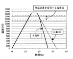
本発明は、BaTiO3系酸化物におけるBaの一部をBiおよびA(Aはアルカリ金属の少なくとも一種の元素であってNaを必須で含む)で置換した組成を有する非鉛の半導体磁器組成物の製造方法において、焼成の際に図1に示すような降温過程で降温速度を変える温度パターン、即ち、1350℃超の温度で焼成した後、150℃/h以下の降温速度で降温を始め、その後、1150℃以上1350℃以下の範囲の間で150℃/h超の降温速度に変える降温過程を適用する。これにより、抵抗温度係数αを大きくすることができることを知見した。
この要因は、降温過程でNaが粒界に析出することによる。Naが粒界に析出することで抵抗温度係数αが大きくなる理由は、推定であるが、Naが粒界に析出することで粒界準位が大きくなり、粒界でのショットキー障壁が増大したためと考えられる。
The present invention relates to a lead-free semiconductor ceramic composition having a composition in which a part of Ba in a BaTiO 3 oxide is substituted with Bi and A (A is an element of at least one alkali metal and contains Na as an essential element). In this manufacturing method, a temperature pattern in which the temperature lowering rate is changed in the temperature lowering process as shown in FIG. 1 at the time of firing, that is, after firing at a temperature exceeding 1350 ° C., temperature lowering starts at a temperature lowering rate of 150 ° C./h or less. After that, a temperature lowering process is applied to change the temperature decreasing rate to over 150 ° C / h between 1150 ° C and 1350 ° C. As a result, it has been found that the temperature coefficient of resistance α can be increased.
This factor is due to the precipitation of Na at the grain boundaries during the cooling process. The reason why the temperature coefficient of resistance α increases when Na precipitates at the grain boundaries is presumed, but when Na precipitates at the grain boundaries, the grain boundary level increases and the Schottky barrier at the grain boundaries increases. It is thought that it was because.
より具体的には以下のように考えられる。
焼成の際、特定の温度以上ではBaの一部をBiおよびAで置換した場合、特定の温度以上では、Biがより多く揮発し、それに伴い価数調整で余剰となった結晶粒中のNaが粒界側に移動する。一方で、粒界に存在するNaは粒界から結晶粒の3重点に存在する異相側に移動するという現象が起こる。Biが揮発している間は粒内から粒界へのNaの供給が起こって粒界のNa量は増加するが、その後Biが揮発しなくなると、Naは粒界から異相側への移動が優勢となって粒界のNa量は減少する。
ここで、Na量が増加する温度域は高温側にあり、Na量が減少する温度域は低温側にある。両者の温度域の境界は降温過程における1150℃以上1350℃以下の間にあることが分かった。
よって、高温側の温度域は150℃/h以下の速度で降温することで時間をかけてNaを粒界に集めて増加させ、その後、低温側の温度域に移行したとき150℃/h超の速度で降温することでNaが粒界から異相へ移動する時間を短縮し、Naの移動を抑制することができる。
その結果、従来の製造方法で作製したものよりも粒界に存在するNa量が多い半導体磁器組成物を得ることができたものと推定される。
More specifically, it is considered as follows.
At the time of firing, when a part of Ba is replaced with Bi and A at a specific temperature or higher, Bi is volatilized more at a specific temperature or higher, and the Na in the crystal grains that have become surplus in the valence adjustment accordingly. Moves to the grain boundary side. On the other hand, a phenomenon occurs in which Na present at the grain boundary moves from the grain boundary to the different phase side present at the triple point of the crystal grain. While Bi is volatilized, Na supply from the grain to the grain boundary occurs and the amount of Na in the grain boundary increases, but when Bi stops volatilizing thereafter, Na moves from the grain boundary to the heterogeneous side. It becomes dominant and the amount of Na in the grain boundary decreases.
Here, the temperature range where the Na amount increases is on the high temperature side, and the temperature range where the Na amount decreases is on the low temperature side. It was found that the boundary between both temperature ranges was between 1150 ℃ and 1350 ℃ in the cooling process.
Therefore, the temperature range on the high temperature side is over 150 ° C / h when the temperature is lowered at a rate of 150 ° C / h or less to collect and increase Na at the grain boundaries over time and then move to the low temperature range. When the temperature is lowered at a rate of Na, the time for Na to move from the grain boundary to the different phase can be shortened, and the movement of Na can be suppressed.
As a result, it is presumed that a semiconductor ceramic composition having a larger amount of Na present at the grain boundaries than that produced by the conventional production method could be obtained.
ここで焼成は1350℃超の温度で行う。焼成の温度が1350℃以下であると、抵抗温度係数αが小さく、PTC素子としての特性が不十分になるという問題がある。1400℃以上とすることが好ましい。但し焼成温度が1500℃を超えると、半導体磁器組成物が焼成中に軟化して所望の形状にならなくなったり抵抗温度係数αが小さくなりやすいため、焼成温度は1500℃以下とすることが好ましい。
1350℃超の保持温度からの降温は150℃/h以下の降温速度で行う。ここでの降温速度が150℃/h超であると、抵抗温度係数αが大きくならずに4.5%/℃未満になる。ここでの降温速度は120℃/h以下とすることが好ましい。
Here, the firing is performed at a temperature higher than 1350 ° C. When the firing temperature is 1350 ° C. or lower, there is a problem that the temperature coefficient of resistance α is small and the characteristics as a PTC element become insufficient. The temperature is preferably 1400 ° C. or higher. However, if the firing temperature exceeds 1500 ° C., the semiconductor ceramic composition is softened during firing and does not become a desired shape, and the resistance temperature coefficient α tends to be small. Therefore, the firing temperature is preferably 1500 ° C. or less.
The temperature lowering from the holding temperature exceeding 1350 ° C is performed at a temperature decreasing rate of 150 ° C / h or less. If the temperature lowering rate here exceeds 150 ° C./h, the resistance temperature coefficient α does not increase and becomes less than 4.5% / ° C. Here, the temperature lowering rate is preferably 120 ° C./h or less.
その後、1150℃以上1350℃以下の範囲で降温速度を変える。降温速度を変えるタイミングが、1150℃未満もしくは1350℃超では抗温度係数αを増加させる効果は得られない。具体的には、抵抗温度係数αが4.5%/℃以上にできない。降温速度を変えるタイミングは、温度が1180℃以上1320℃以下の範囲に設定することがさらに好ましい。
また降温速度を変えてからの降温速度は150℃/h超とする。150℃/h以下では抵抗温度係数αを増加させる効果は得られず、抵抗温度係数αが4.5%/℃以上にならない。ここでの降温速度は180℃/h以上とすることがより好ましい。また、降温速度を150℃/h超とする温度域は、少なくとも800℃迄冷却される範囲とすることが好ましい。
After that, the temperature drop rate is changed in the range of 1150 ℃ to 1350 ℃. If the timing of changing the temperature drop rate is less than 1150 ° C or more than 1350 ° C, the effect of increasing the temperature coefficient α cannot be obtained. Specifically, the resistance temperature coefficient α cannot be 4.5% / ° C. or more. The timing for changing the temperature drop rate is more preferably set in a range of 1180 ° C. or higher and 1320 ° C. or lower.
In addition, the cooling rate after changing the cooling rate is over 150 ° C / h. If it is 150 ° C./h or less, the effect of increasing the temperature coefficient of resistance α cannot be obtained, and the temperature coefficient of resistance α does not exceed 4.5% / ° C. The temperature lowering rate here is more preferably 180 ° C./h or more. Moreover, it is preferable that the temperature range in which the temperature lowering rate exceeds 150 ° C./h is a range in which the temperature is cooled to at least 800 ° C.
焼成の際の雰囲気は、特に規定しないが、例えば大気中または還元雰囲気中、あるいは低酸素濃度の不活性ガス雰囲気とすることができる。特に酸素濃度1%未満の雰囲気中で行うことが好ましい。酸素濃度が1%未満であれば、室温比抵抗を低減する効果も得ることができる。 The atmosphere at the time of firing is not particularly defined, but can be, for example, the air or a reducing atmosphere, or an inert gas atmosphere having a low oxygen concentration. It is particularly preferable to carry out in an atmosphere having an oxygen concentration of less than 1%. If the oxygen concentration is less than 1%, the effect of reducing the room temperature resistivity can also be obtained.
焼成温度での保持時間は1時間以上10時間以下とすることが好ましい。保持時間が1時間未満では焼結が不十分となる場合がある。一方、保持時間が10時間を超えると、粒界に析出しているNaが粒界から拡散し、結晶同士の間に正方晶ではない別の相を形成し、その結果として抵抗温度係数αが小さくなってしまう可能性がある。保持時間はより好ましくは2時間以上6時間以下である。 The holding time at the firing temperature is preferably 1 hour or more and 10 hours or less. If the holding time is less than 1 hour, sintering may be insufficient. On the other hand, when the holding time exceeds 10 hours, Na precipitated at the grain boundary diffuses from the grain boundary, forms another phase that is not a tetragonal crystal between the crystals, and as a result, the temperature coefficient of resistance α is There is a possibility of becoming smaller. The holding time is more preferably 2 hours or longer and 6 hours or shorter.
本発明において、焼成前の製造工程は既知の製造方法を適用できる。
以下に、焼成前の製造工程の一例を示して本発明を説明するが、本発明はこの製造方法に捕らわれるものではない。
In the present invention, a known production method can be applied to the production process before firing.
Hereinafter, the present invention will be described with reference to an example of a manufacturing process before firing, but the present invention is not limited to this manufacturing method.
本発明の半導体磁器組成物を得るための製造方法は、例えば、図2に示すような以下の(Step1)〜(Step5)の工程を持つ製造方法を採用できる。
(Step1) (BiA)TiO3系(Aはアルカリ金属の少なくとも一種の元素であってNaを含む)の第1の原料と、(BaR)[TiM]O3(RはYを含む希土類元素のうち少なくとも一種、MはNb、Ta、Sbのうち少なくとも一種であり、R,Mは少なくともどちらか一方が必須である)系の第2の原料をそれぞれ用意し、
(Step2) 前記第1の原料を700℃以上950℃以下で仮焼、前記第2の原料を900℃以上1300℃以下で仮焼し、
(Step3) 仮焼したそれぞれの材料を混合して第3の原料とし、
(Step4) 成形し、
(Step5) 1350℃を超える温度で焼成する。
以下にこの製造方法について説明する。
As a manufacturing method for obtaining the semiconductor ceramic composition of the present invention, for example, a manufacturing method having the following steps (Step 1) to (Step 5) as shown in FIG. 2 can be adopted.
(Step 1) (BiA) TiO 3 system (A is at least one element of alkali metal and contains Na) and (BaR) [TiM] O 3 (R is a rare earth element containing Y) And at least one of them, M is at least one of Nb, Ta, and Sb, and at least one of R and M is essential).
(Step 2) The first raw material is calcined at 700 ° C. or higher and 950 ° C. or lower, the second raw material is calcined at 900 ° C. or higher and 1300 ° C. or lower,
(Step3) Mix each calcined material to make the third raw material,
(Step4) Molding,
(Step 5) Firing at a temperature exceeding 1350 ° C.
This manufacturing method will be described below.
(Step1)について詳述する。(BiA)TiO3系の第1の原料は、原料粉末となるA2CO3、Bi2O3、TiO2を混合して作製する。なお、(BiA)TiO3系の第1の原料とは、(BiA)TiO3酸化物を形成するための原料を指す。
また、(BaR)[TiM]O3系の第2の原料は、BaCO3、TiO2、R,Mの原料粉末、例えば、La2O3等のR元素酸化物や、Nb2O5等のM元素酸化物を混合して作製する。R,Mは半導体化元素として用いるものである。なお、(BaR)[TiM]O3系の第2の原料とは、(BaR)[TiM]O3酸化物を形成するための原料を指す。
(Step 1) will be described in detail. The (BiA) TiO 3 -based first raw material is prepared by mixing A 2 CO 3 , Bi 2 O 3 , and TiO 2 as raw material powders. Note that the (BiA) TiO 3 -based first raw material refers to a raw material for forming the (BiA) TiO 3 oxide.
The (BaR) [TiM] O 3 -based second raw material is a raw material powder of BaCO 3 , TiO 2 , R, M, for example, an R element oxide such as La 2 O 3 , Nb 2 O 5, etc. It is made by mixing the M element oxide. R and M are used as semiconducting elements. Note that the (BaR) [TiM] O 3 -based second raw material refers to a raw material for forming the (BaR) [TiM] O 3 oxide.
(Step1)の工程においては、第1の原料及び第2の原料ともに、原料粉末の混合の際に、原料粉末の粒度に応じて粉砕を施してもよい。また、原料粉末の混合は純水やエタノールを用いた湿式混合または乾式混合のいずれでもよいが、乾式混合を行うと、組成ずれをより防止しやすい。なお、第1の原料として、A2CO3、Bi2O3、TiO2などの他に、別のA化合物、Bi化合物、Ti化合物を用いてもよい。また、第2の原料も同様に、BaCO3、TiO2などの他に、別のBa化合物、Ti化合物を用いてもよい。 In the step (Step 1), both the first raw material and the second raw material may be pulverized according to the particle size of the raw material powder when the raw material powder is mixed. The raw material powder may be mixed by either wet mixing using pure water or ethanol or dry mixing. However, when dry mixing is performed, compositional deviation is more easily prevented. In addition to A 2 CO 3 , Bi 2 O 3 , TiO 2, etc., another A compound, Bi compound, or Ti compound may be used as the first raw material. Similarly, other Ba compounds and Ti compounds may be used for the second raw material in addition to BaCO 3 , TiO 2 and the like.
(Step2)の(BiA)TiO3系の第1の原料の仮焼について詳述する。
第1の原料の仮焼温度は700℃以上950℃以下とする。仮焼温度が700℃未満では未反応のA2CO3やBi、Tiと未反応のA2Oが、炉内雰囲気の水分あるいは湿式混合の場合はその溶媒と反応して発熱し、組成が所望の値からずれてPTC特性が不安定になりやすい。一方、仮焼温度が950℃を超えると、Biの揮散が進み、組成ずれを起こし、異相の生成が促進されてしまう。その他にも仮焼に用いる匣鉢との反応が増大して劣化を速めてしまうという問題があるため望ましくない。
仮焼時間は0.5時間以上10時間以下が好ましい。仮焼時間が0.5時間未満では、仮焼温度が700℃未満のときと同様の理由で、得られるPTC特性が不安定になりやすい。仮焼時間が10時間を超えると、仮焼温度が950℃を超えるときと同様の理由で、異相の生成が促進されやすくなる。1時間以上8時間とすることがより好ましい。
第1の原料の仮焼は大気中で行うことが好ましい。
また、Biの揮発を抑制するため、第1の原料の仮焼温度は、第1の原料の仮焼温度よりも低い温度とすることが好ましい。
The calcination of the (BiA) TiO 3 -based first raw material in (Step 2) will be described in detail.
The calcining temperature of the first raw material is 700 ° C. or higher and 950 ° C. or lower. If the calcining temperature is less than 700 ° C, unreacted A 2 CO 3 , Bi, Ti and unreacted A 2 O react with the moisture in the furnace atmosphere or in the case of wet mixing, and generate heat, resulting in a composition. The PTC characteristic tends to become unstable due to deviation from the desired value. On the other hand, when the calcining temperature exceeds 950 ° C., the volatilization of Bi proceeds, causing a composition shift and promoting the generation of a different phase. In addition, there is a problem that the reaction with the mortar used for calcination increases and the deterioration is accelerated, which is not desirable.
The calcination time is preferably 0.5 hours or more and 10 hours or less. When the calcination time is less than 0.5 hours, the obtained PTC characteristics are likely to be unstable for the same reason as when the calcination temperature is less than 700 ° C. When the calcining time exceeds 10 hours, the generation of a heterogeneous phase is easily promoted for the same reason as when the calcining temperature exceeds 950 ° C. More preferably, it is 1 hour or more and 8 hours.
The calcination of the first raw material is preferably performed in the air.
In order to suppress the volatilization of Bi, it is preferable that the calcining temperature of the first raw material is lower than the calcining temperature of the first raw material.
(Step2)の(BaR)[TiM]O3系の第2の原料の仮焼について詳述する。
第2の原料の組成は、前述と同様に、R、Mが共に添加されない組成(y=z=0)でもよいが、得られる半導体磁器組成物の室温比抵抗が大きくなるため、少なくともR,Mのどちらかは必須とすることが好ましい。
第2の原料の仮焼温度は900℃以上1300℃以下とする。仮焼温度が900℃未満であると (BaR)[TiM]O3が完全に形成されず、BaCO3から分解した一部のBaOが水と反応したり、残存したBaCO3の一部が水に溶解したりするため、組成ずれの原因となって特性がばらつく可能性がある。
一方、仮焼温度が1300℃を超えると、仮焼粉の一部が互いに焼結し、後に混合する(BiA)TiO3仮焼粉との固溶の妨げになるため好ましくない。その他にも、仮焼に用いる匣鉢に固着してしまうため仮焼粉の取扱が難しくなることや、匣鉢の劣化を速めるという問題があるため望ましくない。
仮焼時間は0.5時間以上が好ましい。仮焼時間が0.5時間未満では組成ずれの原因となる。上限は特に限定されないが、100時間以下とすることが、後に混合する(BiA)TiO3仮焼粉との固溶を促進できるため好ましい。
第2の原料の仮焼は大気中で行うことが好ましい。
The calcination of the (BaR) [TiM] O 3 -based second raw material in (Step 2) will be described in detail.
As described above, the composition of the second raw material may be a composition in which neither R nor M is added (y = z = 0), but since the room temperature resistivity of the resulting semiconductor ceramic composition is increased, at least R, It is preferable to make one of M essential.
The calcining temperature of the second raw material is 900 ° C. or higher and 1300 ° C. or lower. When the calcining temperature is less than 900 ° C., (BaR) [TiM] O 3 is not completely formed, and some BaO decomposed from BaCO 3 reacts with water, or a part of the remaining BaCO 3 is water. Or the like, it may cause a compositional deviation and the characteristics may vary.
On the other hand, when the calcining temperature exceeds 1300 ° C., a part of the calcined powder is sintered together, which is not preferable because it prevents solid solution with the (BiA) TiO 3 calcined powder to be mixed later. In addition, since it adheres to the mortar used for calcination, it is difficult to handle the calcined powder, and the problem of accelerating the deterioration of the mortar is undesirable.
The calcining time is preferably 0.5 hours or more. If the calcining time is less than 0.5 hours, it causes a composition shift. The upper limit is not particularly limited, but it is preferable that the upper limit is 100 hours or less because solid solution with the (BiA) TiO 3 calcined powder to be mixed later can be promoted.
The calcination of the second raw material is preferably performed in the air.
(Step1)と(Step2)の工程により、Biの揮発が抑制されるとともに、Bi-Aの組成ずれを防止してA元素を含有する異相の生成を抑制し、室温比抵抗を低下させるとともに、キュリー温度のバラツキを抑制することができる。 By the steps of (Step 1) and (Step 2), the volatilization of Bi is suppressed, the composition deviation of Bi-A is prevented, the generation of a heterogeneous phase containing element A is suppressed, and the room temperature resistivity is lowered. Variation in Curie temperature can be suppressed.
(Step3)について詳述する。
第1と第2の各仮焼粉を所定量で配合した後、混合して第3の原料とする。
混合は、純水やエタノールを用いた湿式混合または乾式混合のいずれでもよい。また、仮焼粉の粒度に応じて、混合の後に粉砕するか、あるいは混合と粉砕を同時に行ってもよい。混合、粉砕後の仮焼粉の平均粒度は、0.5μm〜7.0μmが好ましい。さらには、0.8μm〜5.0μmが好ましく、1.0μm〜4.0μmがより好ましい。
(Step 3) will be described in detail.
After the first and second calcined powders are blended in a predetermined amount, they are mixed to obtain a third raw material.
Mixing may be either wet mixing using pure water or ethanol or dry mixing. Further, depending on the particle size of the calcined powder, pulverization may be performed after mixing, or mixing and pulverization may be performed simultaneously. The average particle size of the calcined powder after mixing and pulverization is preferably 0.5 μm to 7.0 μm. Furthermore, 0.8 μm to 5.0 μm is preferable, and 1.0 μm to 4.0 μm is more preferable.
第3の原料は、組成式が[(BiA)x(Ba1-yRy)1-x][Ti1-zMz]O3(Aはアルカリ金属の少なくとも一種の元素であってNaを含み、RはYを含む希土類元素のうち少なくとも一種、MはNb、Ta、Sbのうち少なくとも一種)で表わされ、x、y、zが、0<x≦0.2、0≦y≦0.02、0≦z≦0.01を満足するものとすることが好ましい。この組成を得るには、第1と第2の原料を調整しておくことが好ましい。以下、好ましい組成式の規定理由を述べる。 The third raw material has a composition formula of [(BiA) x (Ba 1-y R y ) 1-x ] [Ti 1-z M z ] O 3 (A is at least one element of an alkali metal and Na Wherein R is at least one of rare earth elements including Y, M is at least one of Nb, Ta, and Sb), and x, y, and z are 0 <x ≦ 0.2 and 0 ≦ y ≦ 0.02. , 0 ≦ z ≦ 0.01 is preferably satisfied. In order to obtain this composition, it is preferable to adjust the first and second raw materials. Hereinafter, the reasons for defining the preferred composition formula will be described.
xの範囲を0を超え0.2以下とすることでキュリー温度を130℃〜200℃にすることができる。xが0.2を超えてしまうと異相ができ易くなるため好ましくない。xの範囲は0.03以上0.1以下がさらに好ましい。 Curie temperature can be 130 degreeC-200 degreeC by making the range of x exceed 0 and 0.2 or less. If x exceeds 0.2, it is not preferable because a different phase is easily formed. The range of x is more preferably 0.03 or more and 0.1 or less.
R、Mが共に添加されない組成(y=z=0)でもよい。但し、低電圧用途として用いられるヒーター素子に用いる場合には、y=z=0だと室温比抵抗が200Ωcmを超えて効率が下がるため、y+z>0とすることが好ましい。但しこの場合でもRとMの両方を必須とする必要はなく、少なくともどちらか一方を用いればよい。 A composition in which neither R nor M is added (y = z = 0) may be used. However, when it is used for a heater element used for a low voltage application, if y = z = 0, the room temperature specific resistance exceeds 200 Ωcm and the efficiency is lowered. Therefore, it is preferable to satisfy y + z> 0. However, even in this case, both R and M are not necessarily required, and at least one of them may be used.
Rのyの値は、0<y≦0.02が好ましい範囲である。yが0では組成物が十分に半導体化し難い。また、0.02を超えると室温比抵抗が大きくなりやすい。yの値を変化させることで原子価制御ができる。但し、BaTiO3系酸化物におけるBaの一部をBiおよびAで置換した系において組成物の原子価制御を行う場合、3価の陽イオンを半導体化元素として添加すると半導体化の効果が1価のAイオンの存在のために低下し、室温比抵抗が高くなるという問題がある。そのため、より好ましい範囲は0.002≦y≦0.02である。RはYを含む希土類(Sc,La,Ce,Pr,Nd,Pm,Sm,Eu,Gd,Tb,Dy,Ho,Tb,Tm,Yb,Lu)から選ばれる少なくとも一種以上の元素であり、特にLa,Yが優れたPTC特性を得られるため好ましい。 The value of y in R is preferably in the range of 0 <y ≦ 0.02. When y is 0, the composition is not sufficiently semiconductive. If it exceeds 0.02, the room temperature resistivity tends to increase. The valence can be controlled by changing the value of y. However, when the valence control of the composition is performed in a system in which a part of Ba in the BaTiO 3 oxide is substituted with Bi and A, the addition of a trivalent cation as a semiconducting element results in a monovalent effect. There is a problem that the room temperature resistivity increases due to the presence of A ions. Therefore, a more preferable range is 0.002 ≦ y ≦ 0.02. R is at least one element selected from rare earths including Y (Sc, La, Ce, Pr, Nd, Pm, Sm, Eu, Gd, Tb, Dy, Ho, Tb, Tm, Yb, Lu), In particular, La and Y are preferable because excellent PTC characteristics can be obtained.
M量を示すzは、0<z≦0.01が好ましい範囲である。zが0では原子価制御ができずに組成物が十分に半導体化し難い。また、z=0.01を超えると室温比抵抗が高くなったりキュリー温度が低下しやすい。より好ましい範囲は0.001≦z≦0.005である。Mは特にNbが優れたPTC特性を得られるため好ましい。 Z representing the amount of M is preferably in the range of 0 <z ≦ 0.01. When z is 0, the valence cannot be controlled and the composition is not easily made into a semiconductor. On the other hand, if z exceeds 0.01, the room temperature resistivity tends to increase or the Curie temperature tends to decrease. A more preferable range is 0.001 ≦ z ≦ 0.005. M is particularly preferable because Nb can provide excellent PTC characteristics.
BiとAの比は1:1が良い。但し材料の配合時はこの比が1:1であっても、仮焼や焼成の工程によりBiが揮散してBiとAの比にずれが生じることで焼結体では1:1になっていない場合も本発明に含まれる。Bi:A=0.78〜1.55:1の範囲で許容でき、この範囲内であれば異相の増大を抑制できるので、室温比抵抗の増大や経時変化を抑制できる。さらに好ましい範囲はBi:A=0.90〜1.2:1である。 A good ratio of Bi and A is 1: 1. However, even when this ratio is 1: 1 at the time of blending the materials, Bi is volatilized by the calcination or firing process, and the ratio of Bi and A is shifted, so that the sintered body is 1: 1. It is included in this invention also when there is no. Bi: A = 0.78 to 1.55: 1 is acceptable, and if it is within this range, the increase in heterogeneous phase can be suppressed, so that the increase in room temperature resistivity and change with time can be suppressed. A more preferable range is Bi: A = 0.90 to 1.2: 1.
なお、これら以外に焼結助剤としてSi原料、Ca原料を用いることができる。これらの焼結助剤を用いた場合は、上記組成式にSi,Caが含まれることもある。
なお、焼結助剤は後述の工程で添加することもできる。
In addition to these, Si raw materials and Ca raw materials can be used as sintering aids. When these sintering aids are used, Si and Ca may be included in the above composition formula.
In addition, a sintering auxiliary agent can also be added at the process mentioned later.
(Step4)について詳述する。
混合物を成形する。成形前に必要に応じて混合物を造粒装置によって造粒してもよい。成形後の成形体密度は2.5〜4.2g/cm3が好ましい。
(Step 4) will be described in detail.
Mold the mixture. You may granulate a mixture with a granulator as needed before shaping | molding. The compact density after molding is preferably 2.5 to 4.2 g / cm 3 .
また、成形する前に、前記第3の原料を900℃以上1250℃以下で熱処理しておくことが好ましい。この熱処理で第1の仮焼粉と第2の仮焼粉の組成を均一化させることができる。均一化された状態は結晶粒が育成される直前の状態に近く、その後の焼結でこの組成が大きく変わらないまま結晶粒を育成させることができるので、結晶粒の内と外の組織形態を意図的に変えやすくなる。例えば、この熱処理の後にYを添加し、その後、成形および焼成をすることで、Yが結晶粒の外に偏析したことで経時変化が小さくなった半導体磁器組成物を得ることができる。
熱処理の温度は、この工程により両者の組成のX線回折の回折線ピークが同じ位置、つまり固溶状態になる温度とすることが好ましい。900℃未満ではBiが十分に拡散されない。1250℃を超えると(BiA)TiO3系の融点が1250℃付近であるためにBiが炉内雰囲気へ蒸発してしまったり、一部が焼結し熱処理用の匣鉢に固着して取扱が難しくなったり、匣鉢の劣化を速めてしまう問題がある。Biの蒸発を防ぐためには低い温度で熱処理することが望ましいが、低すぎると熱処理を長時間行う必要がある。さらに好ましい熱処理温度は1000℃以上1200℃以下である。
Further, it is preferable that the third raw material is heat-treated at 900 ° C. to 1250 ° C. before molding. By this heat treatment, the composition of the first calcined powder and the second calcined powder can be made uniform. The homogenized state is close to the state immediately before the crystal grains are grown, and the crystal grains can be grown without significant change in the composition by subsequent sintering. It becomes easy to change intentionally. For example, by adding Y after this heat treatment, followed by molding and firing, a semiconductor ceramic composition having a small change with time due to Y segregating outside the crystal grains can be obtained.
The temperature of the heat treatment is preferably set to a temperature at which the diffraction line peaks of the X-ray diffraction of both compositions are in the same position, that is, a solid solution state by this step. Below 900 ° C, Bi is not sufficiently diffused. If it exceeds 1250 ° C, the melting point of (BiA) TiO 3 system is around 1250 ° C, so Bi will evaporate into the furnace atmosphere, or part of it will sinter and stick to the mortar for heat treatment. There are problems that become difficult and accelerate the deterioration of the mortar. In order to prevent the evaporation of Bi, it is desirable to perform heat treatment at a low temperature, but if it is too low, it is necessary to perform the heat treatment for a long time. A more preferable heat treatment temperature is 1000 ° C. or higher and 1200 ° C. or lower.
熱処理時間は0.5時間以上20時間以下が好ましい。0.5時間より短い場合は(BaR)[TiM]O3系の仮焼粉と(BiA)TiO3系の仮焼粉の固溶が安定せず得られるPTC特性が安定しなくなる。これに対して20時間を超えるとBiの揮散が多くなり組成ずれを起こしやすくなる。好ましい熱処理時間は1時間以上12時間以下、さらに好ましくは1.5時間以上6時間以下である。この第3の原料の熱処理は、大気中で行うことが好ましい。 The heat treatment time is preferably 0.5 hours or more and 20 hours or less. When the time is shorter than 0.5 hour, the solid solution of the (BaR) [TiM] O 3 -based calcined powder and the (BiA) TiO 3 -based calcined powder is not stable, resulting in unstable PTC characteristics. On the other hand, when it exceeds 20 hours, the volatilization of Bi increases and the composition shift tends to occur. The heat treatment time is preferably 1 hour or more and 12 hours or less, more preferably 1.5 hours or more and 6 hours or less. The heat treatment of the third raw material is preferably performed in the atmosphere.
(Step5)の焼成については先に説明したとおりであり、説明を省略する。 The firing in (Step 5) is as described above, and the description is omitted.
本発明の製造方法により得られる半導体磁器組成物は、結晶粒の粒界におけるNa量が3mol%以上とすることができる。このNa量が3mol%以上とすることで、抵抗温度係数αが4.5%/℃以上の半導体磁器組成物になる。
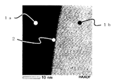
本発明において、結晶粒界とは、図3に示すように、異なる二つの正方晶の結晶粒(BaTiO3系酸化物)1a,1bの境界面を指す。粒界Na量はその境界面の断面中央部を走査型透過電子顕微鏡(Scanning Transmission Electron Microscope:STEM)により10万倍の視野で測定したものである。測定方法の詳細は後述する。
In the semiconductor ceramic composition obtained by the production method of the present invention, the amount of Na at the grain boundary of the crystal grains can be 3 mol% or more. By setting the amount of Na to 3 mol% or more, a semiconductor ceramic composition having a temperature coefficient of resistance α of 4.5% / ° C. or more is obtained.
In the present invention, the crystal grain boundary means a boundary surface between two different tetragonal crystal grains (BaTiO 3 -based oxides) 1a and 1b as shown in FIG. The amount of grain boundary Na is measured at the center of the cross section of the boundary surface with a scanning transmission electron microscope (STEM) in a field of view of 100,000 times. Details of the measurement method will be described later.
この半導体磁器組成物は、BaTiO3系酸化物におけるBaの一部をBiおよびNaで置換した組成を有する結晶粒を有する。
その中でも、組成式が[(BiA)x(Ba1-yRy)1-x][Ti1-zMz]O3(Aはアルカリ金属の少なくとも一種の元素であってNaを必須で含み、RはYを含む希土類元素のうち少なくとも一種、MはNb、Ta、Sbのうち少なくとも一種)で表わされ、x、y、zが、0<x≦0.2、0≦y≦0.02、0≦z≦0.01を満足する結晶粒を有するものが好ましい。
各数値の限定理由は、先の第3の原料で説明した組成式の理由と同じで有り、説明を省略する。
This semiconductor ceramic composition has crystal grains having a composition in which a part of Ba in the BaTiO 3 oxide is substituted with Bi and Na.
Among them, the composition formula is [(BiA) x (Ba 1-y R y ) 1-x ] [Ti 1-z M z ] O 3 (A is at least one element of an alkali metal and Na is essential. And R is represented by at least one of rare earth elements including Y, M is represented by at least one of Nb, Ta, and Sb), and x, y, and z are 0 <x ≦ 0.2, 0 ≦ y ≦ 0.02, Those having crystal grains satisfying 0 ≦ z ≦ 0.01 are preferable.
The reason for limiting each numerical value is the same as the reason for the composition formula described in the third raw material, and a description thereof will be omitted.
本発明の半導体磁器組成物は、板状に加工し、その板の両面に電極を設けることでPTC素子とすることができる。電極の形成方法は既知の手段を採用できるが、電極ペーストを塗布した後に焼付ける手段が低コストである。 The semiconductor ceramic composition of the present invention can be made into a PTC element by processing it into a plate shape and providing electrodes on both sides of the plate. As a method for forming the electrode, known means can be adopted, but a means for baking after applying the electrode paste is low in cost.
本発明において、結晶粒界におけるNa量の測定、抵抗温度係数α、室温比抵抗R25の評価方法は以下のように行った。 In the present invention, measurement of the amount of Na at the crystal grain boundary, evaluation method of the resistance temperature coefficient α, and the room temperature specific resistance R 25 were performed as follows.
(結晶粒界におけるNa量)
まず、JEOL社製の原子分解能分析電子顕微鏡(型番JEM-ARM200F)を用いて、2つの結晶粒の断面(粒界)が隣接した視野を定める。これらの結晶粒がBaTiO3系の正方晶であることを確認する。その後、この二つの結晶の境界面をSTEM-EDXで元素分析する。倍率は10万倍とする。加速電圧は200kV、ビーム径は0.2 nmとする。任意に境界面の5箇所を測定し、その平均値を結晶粒界におけるNa量とする。
(Na amount at grain boundaries)
First, using a JEOL atomic resolution analytical electron microscope (model number JEM-ARM200F), a field of view where the cross-sections (grain boundaries) of two crystal grains are adjacent to each other is defined. It is confirmed that these crystal grains are BaTiO 3 -based tetragonal crystals. After that, the interface between these two crystals is subjected to elemental analysis with STEM-EDX. The magnification is 100,000 times. The acceleration voltage is 200 kV and the beam diameter is 0.2 nm. Arbitrarily 5 points on the boundary surface are measured, and the average value is taken as the amount of Na at the grain boundary.
(抵抗温度係数α)
抵抗温度係数αは、半導体磁器組成物を260℃まで昇温しながら抵抗−温度特性を測定して算出した。
尚、抵抗温度係数αは次式で定義される。
α=(lnRL-lnRC)×100/(TL-TC)
なお図4(横軸:温度、縦軸(対数表記):比抵抗)に示すように、RLは260℃の比抵抗、TLは260℃、TCはキュリー温度、RCはTCにおける比抵抗である。ここでキュリー温度TCは比抵抗が室温比抵抗R25の2倍となる温度とした。
(Resistance temperature coefficient α)
The temperature coefficient of resistance α was calculated by measuring resistance-temperature characteristics while raising the temperature of the semiconductor ceramic composition to 260 ° C.
The resistance temperature coefficient α is defined by the following equation.
α = (lnR L -lnR C ) × 100 / (T L -T C )
As shown in Fig. 4 (horizontal axis: temperature, vertical axis (logarithmic notation): specific resistance), R L is the specific resistance at 260 ° C, T L is 260 ° C, T C is the Curie temperature, and R C is T C The specific resistance at. Here the Curie temperature T C was the temperature at which the resistivity becomes twice the room temperature resistivity R 25.
(室温比抵抗R25)
半導体磁器組成物の室温比抵抗R25(Ωcm)は、25℃、4端子法で測定した。
(Room temperature resistivity R 25 )
The room temperature resistivity R 25 (Ωcm) of the semiconductor ceramic composition was measured at 25 ° C. by a four-terminal method.
(実施例)
焼成工程における降温過程での降温条件を変え、それに伴う抵抗温度係数αの関係を調べた。
図2に示すように、原料として、(BiA)TiO3系の第1の原料と(BaR)[TiM]O3系の第2の原料をそれぞれ用意した(Step1)。本実施例では、(BiA)TiO3系の第1の原料として、Na2CO3、Bi2O3、TiO2の原料粉末を準備し、BiとNaのモル比率Bi/Naが1.05の(Bi0.525Na0.500)TiO3となるように配合し、乾式混合した。また、(BaR)[TiM]O3系の第2の原料としてBaCO3、TiO2、La2O3の原料粉末を準備し、(Ba0.994La0.006)TiO3となるように配合し、純水で混合した。
前記第1の原料を700℃以上950℃以下で仮焼し、前記第2の原料を900℃以上1300℃以下で仮焼した(Step2)。本実施例では、得られた第1の原料を800℃で2時間大気中で仮焼し、(BiA)TiO3系の仮焼粉を用意した。また、第2の原料を1200℃で4時間大気中で仮焼し、(BaR)[TiM]O3系の仮焼粉を用意した。
その後、仮焼したそれぞれの材料を混合した(Step3)。本実施例では、(BiA)TiO3系の仮焼粉と(BaR)[TiM]O3系の仮焼粉を、0.085:0.915の比で混合し、[(BiNa)0.085(Ba0.994La0.006)0.915]TiO3となるように混合した。この材料を、純水を媒体としてポットミルにより、平均粒径が2.0μm〜3.0μmになるまで混合、粉砕し、その後、乾燥させた。
(Example)
The temperature lowering conditions in the temperature lowering process in the firing process were changed, and the relationship of the resistance temperature coefficient α associated therewith was investigated.
As shown in FIG. 2, a (BiA) TiO 3 -based first material and a (BaR) [TiM] O 3 -based second material were prepared as raw materials (Step 1). In this example, raw material powder of Na 2 CO 3 , Bi 2 O 3 , TiO 2 was prepared as the first raw material of (BiA) TiO 3 system, and the molar ratio Bi / Na Bi / Na of 1.05 ( Bi 0.525 Na 0.500 ) TiO 3 was blended and dry mixed. In addition, a raw material powder of BaCO 3 , TiO 2 , and La 2 O 3 was prepared as the second raw material of the (BaR) [TiM] O 3 system, blended so as to be (Ba 0.994 La 0.006 ) TiO 3, and pure Mixed with water.
The first raw material was calcined at 700 ° C. to 950 ° C. and the second raw material was calcined at 900 ° C. to 1300 ° C. (Step 2). In this example, the obtained first raw material was calcined in the air at 800 ° C. for 2 hours to prepare a (BiA) TiO 3 -based calcined powder. Further, the second raw material was calcined in the atmosphere at 1200 ° C. for 4 hours to prepare a (BaR) [TiM] O 3 -based calcined powder.
Thereafter, the calcined materials were mixed (Step 3). In this example, (BiA) TiO 3 -based calcined powder and (BaR) [TiM] O 3 -based calcined powder were mixed at a ratio of 0.085: 0.915, and [(BiNa) 0.085 (Ba 0.994 La 0.006 ) 0.915 ] TiO 3 was mixed. This material was mixed and pulverized with a pot mill using pure water as a medium until the average particle size became 2.0 μm to 3.0 μm, and then dried.
この原料を900℃以上1250℃以下で熱処理した。具体的には、この原料を1150℃で、4時間大気中で熱処理を行った。この温度で処理した第3の原料は、X線回折で測定すると(BaR)[TiM]O3系の仮焼粉と(BiA)TiO3系の仮焼粉のそれぞれの回折線がひとつになっていた。
その後、本実施例では、Ba6Ti17O40とY2O3とCaCO3を添加した。なお、Ba6Ti17O40は焼成条件を安定化させる効果を持つ。Y2O3は経時変化を抑制する効果を持つ。CaCO3は焼結助剤の効果を持つ。Ba6Ti17O40とY2O3とCaCO3の添加量は、第3の原料を100mol%として、Ba6Ti17O40は0.6mol%、Y2O3は1mol%、CaCO3は2mol%とした。
This raw material was heat-treated at 900 ° C. to 1250 ° C. Specifically, this raw material was heat-treated at 1150 ° C. for 4 hours in the air. The third raw material treated at this temperature has a diffraction line of (BaR) [TiM] O 3 -based calcined powder and (BiA) TiO 3 -based calcined powder as measured by X-ray diffraction. It was.
Thereafter, Ba 6 Ti 17 O 40 , Y 2 O 3 and CaCO 3 were added in this example. Ba 6 Ti 17 O 40 has the effect of stabilizing the firing conditions. Y 2 O 3 has the effect of suppressing changes over time. CaCO 3 has the effect of a sintering aid. The addition amount of Ba 6 Ti 17 O 40 , Y 2 O 3 and CaCO 3 is 100 mol% for the third raw material, 0.6 mol% for Ba 6 Ti 17 O 40 , 1 mol% for Y 2 O 3 and CaCO 3 It was 2 mol%.
その後、成形した(Step4)。本実施例では、PVAを添加、混合し、造粒した。得られた造粒粉を一軸プレス装置で成形し、700℃で脱バインダーした。 Thereafter, molding was performed (Step 4). In this example, PVA was added, mixed, and granulated. The obtained granulated powder was molded with a single screw press machine and debindered at 700 ° C.
その後、焼結した(Step5)。本実施例では、窒素中、酸素濃度0.007vol%(70ppm)の雰囲気にて1440℃、4時間保持した後、表1に示した各降温条件にて降温して焼結体を得た。 Thereafter, sintering was performed (Step 5). In this example, after holding at 1440 ° C. for 4 hours in an atmosphere having an oxygen concentration of 0.007 vol% (70 ppm) in nitrogen, the temperature was lowered under each temperature drop condition shown in Table 1 to obtain a sintered body.
得られた焼結体を10mm×10mm×1.0mmの板状に加工して試験片を作製し、卑金属性のオーミック電極を塗布し、さらにAgを主成分とするカバー電極を塗布して180℃で乾燥後600℃、10分保持で焼き付けて電極を形成した。 The obtained sintered body is processed into a plate of 10 mm x 10 mm x 1.0 mm to produce a test piece, a base metal ohmic electrode is applied, and a cover electrode mainly composed of Ag is further applied at 180 ° C. After drying, the electrode was formed by baking at 600 ° C. for 10 minutes.
焼成時の保持温度からの降温速度、降温速度を変更する温度、変更後の降温速度、抵抗温度係数α、室温比抵抗R25、粒界Na量の測定結果を表1に示す。なお比較例には*を付けて表記した。 Table 1 shows the measurement results of the temperature lowering rate from the holding temperature during firing, the temperature for changing the temperature lowering rate, the temperature falling rate after the change, the resistance temperature coefficient α, the room temperature specific resistance R 25 , and the grain boundary Na amount. Note that the comparative examples are indicated with *.

No.1は降温条件を従来から変更せずに100℃/hで一律に降温した比較用の半導体磁器組成物であるが、その抵抗温度係数αは4.42%/℃と低いものであった。No.2は降温速度を1100℃で変更した比較用の半導体磁器組成物であるが、抵抗温度係数αの増加はNo.1に対して僅かであり、それぞれ4.44%/℃と低いものであった。
対してNo.3,4は降温速度を1200℃と1300℃でそれぞれ変更し、その後の降温速度を300℃/hとした実施例の半導体磁器組成物であるが、抵抗温度係数αはNo.1に対して大幅に増加し、それぞれ5.31%/℃、5.15%/℃といずれも4.5%/℃以上となった。
No. 1 is a comparative semiconductor porcelain composition in which the temperature was lowered uniformly at 100 ° C./h without changing the temperature lowering condition from the past, but its resistance temperature coefficient α was as low as 4.42% / ° C. No. 2 is a comparative semiconductor porcelain composition in which the temperature drop rate was changed at 1100 ° C, but the increase in resistance temperature coefficient α was slight compared to No. 1, which was as low as 4.44% / ° C, respectively. It was.
On the other hand, Nos. 3 and 4 are semiconductor porcelain compositions of Examples in which the temperature drop rate was changed at 1200 ° C. and 1300 ° C., respectively, and the temperature drop rate thereafter was 300 ° C./h, but the resistance temperature coefficient α was No. It increased significantly from 1 and increased to 5.31% / ° C and 5.15% / ° C, respectively, exceeding 4.5% / ° C.
No.5は降温速度を変更する温度を1200℃とし、それ以後の降温速度を200℃/hとした実施例の半導体磁器組成物である。No.3,4と同様に抵抗温度係数αは増大して4.93%/℃となり、4.5%/℃以上となる結果であった。
一方、No.6はNo.5に対して降温速度を50℃/hとして降温した比較用の半導体磁器組成物である。この場合は抵抗温度係数αは4.33%/℃と減少し、4.5%/℃以下となる結果であった。
No. 5 is a semiconductor porcelain composition of an example in which the temperature change rate is 1200 ° C. and the subsequent temperature drop rate is 200 ° C./h. Similar to Nos. 3 and 4, the temperature coefficient of resistance α increased to 4.93% / ° C, which was 4.5% / ° C or higher.
On the other hand, No. 6 is a comparative semiconductor porcelain composition in which the temperature was decreased at a rate of temperature decrease of 50 ° C./h compared to No. 5. In this case, the temperature coefficient of resistance α decreased to 4.33% / ° C. and became 4.5% / ° C. or less.
なお、表1の各半導体磁器組成物の結晶粒の組成を調べたところ、組成式が[(BiA)x(Ba1-yRy)1-x][Ti1-zMz]O3(AはNa,Li,Kのうち少なくとも一種であってNaを含み、RはYを含む希土類元素のうち少なくとも一種、MはNb、Ta、Sbのうち少なくとも一種)で表わされ、x、y、zが、0<x≦0.2、0≦y≦0.02、0≦z≦0.01を満足するものであった。 In addition, when the composition of the crystal grains of each semiconductor ceramic composition in Table 1 was examined, the composition formula was [(BiA) x (Ba 1-y R y ) 1-x ] [Ti 1-z M z ] O 3 (A is at least one of Na, Li and K and contains Na, R is at least one of rare earth elements including Y, M is at least one of Nb, Ta and Sb), x, y and z satisfied 0 <x ≦ 0.2, 0 ≦ y ≦ 0.02, and 0 ≦ z ≦ 0.01.
Claims (5)
1350℃超の温度で焼成した後、150℃/h以下の降温速度で降温を始め、その後、1150℃以上1350℃以下の範囲の間で150℃/h超の降温速度に変える降温過程を有することを特徴とする半導体磁器組成物の製造方法。 A method for producing a semiconductor ceramic composition having a composition in which a part of Ba in a BaTiO 3 -based oxide is substituted with Bi and A (A is at least one element of an alkali metal and contains Na as an essential element),
After firing at a temperature of over 1350 ° C., the temperature starts to drop at a rate of 150 ° C./h or less, and then falls within a range of 1150 ° C. to 1350 ° C. to a temperature drop rate of over 150 ° C./h. A method for producing a semiconductor porcelain composition.
結晶粒の粒界におけるNa量が3mol%以上であることを特徴とする半導体磁器組成物。 A semiconductor ceramic composition obtained by the production method according to claim 1 or 2,
A semiconductor ceramic composition characterized in that the amount of Na at grain boundaries of crystal grains is 3 mol% or more.
Priority Applications (2)
| Application Number | Priority Date | Filing Date | Title |
|---|---|---|---|
| JP2014183887A JP2017197389A (en) | 2014-09-10 | 2014-09-10 | Method for manufacturing semiconductor ceramic composition, semiconductor ceramic composition, and ptc element |
| PCT/JP2015/075111 WO2016039253A1 (en) | 2014-09-10 | 2015-09-03 | Method for manufacturing semiconductor ceramic composition, semiconductor ceramic composition, and ptc element |
Applications Claiming Priority (1)
| Application Number | Priority Date | Filing Date | Title |
|---|---|---|---|
| JP2014183887A JP2017197389A (en) | 2014-09-10 | 2014-09-10 | Method for manufacturing semiconductor ceramic composition, semiconductor ceramic composition, and ptc element |
Publications (1)
| Publication Number | Publication Date |
|---|---|
| JP2017197389A true JP2017197389A (en) | 2017-11-02 |
Family
ID=55459001
Family Applications (1)
| Application Number | Title | Priority Date | Filing Date |
|---|---|---|---|
| JP2014183887A Pending JP2017197389A (en) | 2014-09-10 | 2014-09-10 | Method for manufacturing semiconductor ceramic composition, semiconductor ceramic composition, and ptc element |
Country Status (2)
| Country | Link |
|---|---|
| JP (1) | JP2017197389A (en) |
| WO (1) | WO2016039253A1 (en) |
Family Cites Families (5)
| Publication number | Priority date | Publication date | Assignee | Title |
|---|---|---|---|---|
| US8067325B2 (en) * | 2006-02-27 | 2011-11-29 | Hitachi Metals, Ltd. | Semiconductor ceramic composition |
| JP5099011B2 (en) * | 2006-09-28 | 2012-12-12 | 株式会社村田製作所 | Barium titanate-based semiconductor ceramic composition and PTC element using the same |
| JP5251119B2 (en) * | 2007-12-26 | 2013-07-31 | 日立金属株式会社 | Semiconductor porcelain composition |
| JP5716263B2 (en) * | 2008-06-30 | 2015-05-13 | 日立金属株式会社 | Ceramic sintered body and piezoelectric element |
| JPWO2013157650A1 (en) * | 2012-04-20 | 2015-12-21 | 日立金属株式会社 | Method for producing semiconductor porcelain composition |
-
2014
- 2014-09-10 JP JP2014183887A patent/JP2017197389A/en active Pending
-
2015
- 2015-09-03 WO PCT/JP2015/075111 patent/WO2016039253A1/en active Application Filing
Also Published As
| Publication number | Publication date |
|---|---|
| WO2016039253A1 (en) | 2016-03-17 |
Similar Documents
| Publication | Publication Date | Title |
|---|---|---|
| JP5151477B2 (en) | Semiconductor porcelain composition and method for producing the same | |
| JP5228915B2 (en) | Semiconductor porcelain composition and method for producing the same | |
| WO2013157650A1 (en) | Method for producing semiconductor ceramic composition | |
| JP5251119B2 (en) | Semiconductor porcelain composition | |
| JP5218042B2 (en) | Semiconductor porcelain composition | |
| JP5445640B2 (en) | Method for producing semiconductor porcelain composition | |
| JP5228916B2 (en) | Semiconductor porcelain composition and method for producing the same | |
| JP4765258B2 (en) | Semiconductor porcelain composition | |
| JP5228917B2 (en) | Semiconductor porcelain composition and method for producing the same | |
| JPWO2008053813A1 (en) | Semiconductor porcelain composition and method for producing the same | |
| JP5590494B2 (en) | Manufacturing method of semiconductor ceramic composition-electrode assembly | |
| JP5844507B2 (en) | Method for producing semiconductor porcelain composition and heater using semiconductor porcelain composition | |
| WO2016039253A1 (en) | Method for manufacturing semiconductor ceramic composition, semiconductor ceramic composition, and ptc element | |
| JP5267505B2 (en) | Semiconductor porcelain composition | |
| WO2016002714A1 (en) | Semiconductor ceramic composition and ptc element | |
| JP2010168265A (en) | Method for manufacturing semiconductor ceramic composition | |
| WO2015115421A1 (en) | Manufacturing method for semiconductor ceramic composition, semiconductor ceramic composition, ptc element, and heating element module | |
| TWI406303B (en) | Semiconductor porcelain composition and method of manufacturing the same |