JP2017192002A - Optical signal relay device and relay method - Google Patents
Optical signal relay device and relay method Download PDFInfo
- Publication number
- JP2017192002A JP2017192002A JP2016079903A JP2016079903A JP2017192002A JP 2017192002 A JP2017192002 A JP 2017192002A JP 2016079903 A JP2016079903 A JP 2016079903A JP 2016079903 A JP2016079903 A JP 2016079903A JP 2017192002 A JP2017192002 A JP 2017192002A
- Authority
- JP
- Japan
- Prior art keywords
- signal
- burst
- optical
- reception
- output
- Prior art date
- Legal status (The legal status is an assumption and is not a legal conclusion. Google has not performed a legal analysis and makes no representation as to the accuracy of the status listed.)
- Pending
Links
- 230000003287 optical effect Effects 0.000 title claims abstract description 171
- 238000000034 method Methods 0.000 title claims abstract description 17
- 238000001514 detection method Methods 0.000 claims abstract description 28
- 230000003111 delayed effect Effects 0.000 claims abstract description 27
- 238000006243 chemical reaction Methods 0.000 claims abstract description 7
- 230000001934 delay Effects 0.000 claims description 6
- 238000012544 monitoring process Methods 0.000 claims description 2
- 239000013307 optical fiber Substances 0.000 description 27
- 238000004891 communication Methods 0.000 description 17
- 238000011144 upstream manufacturing Methods 0.000 description 10
- 238000010586 diagram Methods 0.000 description 9
- 230000008878 coupling Effects 0.000 description 8
- 238000010168 coupling process Methods 0.000 description 8
- 238000005859 coupling reaction Methods 0.000 description 8
- 230000005540 biological transmission Effects 0.000 description 5
- 238000012545 processing Methods 0.000 description 4
- 239000013589 supplement Substances 0.000 description 3
- 230000001360 synchronised effect Effects 0.000 description 3
- 239000003990 capacitor Substances 0.000 description 2
- 230000000295 complement effect Effects 0.000 description 2
- 238000007599 discharging Methods 0.000 description 2
- 238000009434 installation Methods 0.000 description 2
- 238000012986 modification Methods 0.000 description 2
- 230000004048 modification Effects 0.000 description 2
- 230000008569 process Effects 0.000 description 2
- 238000011084 recovery Methods 0.000 description 2
- 230000004044 response Effects 0.000 description 2
- 230000009471 action Effects 0.000 description 1
- 230000002457 bidirectional effect Effects 0.000 description 1
- 230000003139 buffering effect Effects 0.000 description 1
- 230000000694 effects Effects 0.000 description 1
- 238000005516 engineering process Methods 0.000 description 1
- 239000000284 extract Substances 0.000 description 1
- 238000012423 maintenance Methods 0.000 description 1
- 230000003252 repetitive effect Effects 0.000 description 1
- 230000000630 rising effect Effects 0.000 description 1
- 238000005070 sampling Methods 0.000 description 1
- 230000008054 signal transmission Effects 0.000 description 1
Images


Classifications
-
- H—ELECTRICITY
- H04—ELECTRIC COMMUNICATION TECHNIQUE
- H04B—TRANSMISSION
- H04B10/00—Transmission systems employing electromagnetic waves other than radio-waves, e.g. infrared, visible or ultraviolet light, or employing corpuscular radiation, e.g. quantum communication
- H04B10/27—Arrangements for networking
- H04B10/272—Star-type networks or tree-type networks
-
- H—ELECTRICITY
- H04—ELECTRIC COMMUNICATION TECHNIQUE
- H04B—TRANSMISSION
- H04B10/00—Transmission systems employing electromagnetic waves other than radio-waves, e.g. infrared, visible or ultraviolet light, or employing corpuscular radiation, e.g. quantum communication
- H04B10/29—Repeaters
-
- H—ELECTRICITY
- H04—ELECTRIC COMMUNICATION TECHNIQUE
- H04L—TRANSMISSION OF DIGITAL INFORMATION, e.g. TELEGRAPHIC COMMUNICATION
- H04L12/00—Data switching networks
- H04L12/28—Data switching networks characterised by path configuration, e.g. LAN [Local Area Networks] or WAN [Wide Area Networks]
- H04L12/44—Star or tree networks
Landscapes
- Engineering & Computer Science (AREA)
- Computer Networks & Wireless Communication (AREA)
- Signal Processing (AREA)
- Physics & Mathematics (AREA)
- Electromagnetism (AREA)
- Computing Systems (AREA)
- Optical Communication System (AREA)
- Small-Scale Networks (AREA)
Abstract
【課題】PONシステムにおいてバースト信号同士の時間間隔を広げることなく、各光バースト信号のプリアンブル部分を補完することができる光信号中継装置および制御方法を提供する。【解決手段】受信した光バースト信号をバースト受信信号に変換する光/電気変換モジュール71において、ひとつのバースト受信信号の終了を検出すれば、所定のリセット時間Trstが経過した後、次のバースト受信信号の検出を始める信号検出部と、バースト受信信号を蓄積して遅延させ、当該遅延されたバースト受信信号を出力する遅延バッファ部73と、所定の時間にわたって、連続バースト受信判定信号を出力する連続バースト信号受信判定部72とを備える。連続バースト受信判定信号が存在する期間にわたって、バッファ部から出力される遅延されたバースト受信信号の同期パターンを、同期パターン信号に切り替えるように制御する。【選択図】図3An optical signal repeater and a control method capable of complementing the preamble portion of each optical burst signal without increasing the time interval between burst signals in a PON system. In an optical / electrical conversion module 71 that converts a received optical burst signal into a burst reception signal, if the end of one burst reception signal is detected, the next burst reception is performed after a predetermined reset time Trst has elapsed. A signal detection unit for starting signal detection, a delay buffer unit 73 for accumulating and delaying burst reception signals and outputting the delayed burst reception signals, and a continuous burst reception determination signal for a predetermined time. A burst signal reception determination unit 72. Control is performed so that the synchronization pattern of the delayed burst reception signal output from the buffer unit is switched to the synchronization pattern signal over a period in which the continuous burst reception determination signal exists. [Selection] Figure 3
Description
本発明は、PON(Passive Optical Network)システムにおいて局側装置(OLT)と宅側装置(ONU)との間の光信号を、光/電気モジュールで光/電気変換した後に、再び電気/光モジュールで光信号に変換して中継する光中継装置に関するものであり、特に宅側装置(ONU)から局側装置(OLT)への光バースト信号の中継技術に関する。 In the PON (Passive Optical Network) system, the optical signal between the station side device (OLT) and the home side device (ONU) is optically / electrically converted by the optical / electrical module, and then again the electrical / optical module. In particular, the present invention relates to a technique for relaying an optical burst signal from a home side apparatus (ONU) to a station side apparatus (OLT).
光加入者線局側装置OLT(Optical Line Terminal;以下「局側装置」という)と、複数の光加入者線終端装置ONU(Optical Network Unit;以下「宅側装置」という)との間を、光ファイバ通信ネットワークを介して、双方向通信する光通信システムがある。
この光通信システムにおいて、局側装置OLTと各宅側装置ONUとの間を、それぞれ光ファイバで放射状に結んだ(Single Star)光ファイバ通信ネットワークが構築され、実用化されている。このネットワークの構成では、システムや通信機器などの構成は簡単になるが、1つの宅側装置ONUが、一本の光ファイバを占有しており、局側装置OLTにこの光ファイバを直接配線接続しなければならない。よって、宅側装置ONUがN局あれば、局側装置OLTから直接配線接続される光ファイバがN本必要となり、光通信システムの低価格化を図るのが困難である。
Between an optical subscriber line station side device OLT (Optical Line Terminal; hereinafter referred to as “station side device”) and a plurality of optical subscriber line termination units ONU (Optical Network Unit; hereinafter referred to as “home side device”), There is an optical communication system that performs two-way communication via an optical fiber communication network.
In this optical communication system, a single star optical fiber communication network in which the station side device OLT and each home device ONU are radially connected by optical fibers has been constructed and put into practical use. In this network configuration, the configuration of the system and communication equipment becomes simple, but one home-side device ONU occupies one optical fiber, and this optical fiber is directly connected to the station-side device OLT by wiring. Must. Therefore, if the home-side apparatus ONU has N stations, N optical fibers that are directly connected from the station-side apparatus OLT are required, and it is difficult to reduce the price of the optical communication system.
そこで、局側装置OLTから配線接続される1本の光ファイバを、複数の宅側装置ONUで共有する光通信システムとして、PON(Passive Optical Network)システムが実用化されている。
このPONシステムでは、特に外部からの電源供給を必要とせずに入力された信号を受動的に分岐・多重する受動型光分岐器(以下、単に「光カプラ」ともいう)と、局側装置OLTとが光ファイバを介して接続されている。さらに光カプラで分岐された光ファイバが、宅側装置ONUの数に合わせて備えられている。
Therefore, a PON (Passive Optical Network) system has been put to practical use as an optical communication system in which one optical fiber connected by wiring from the station side device OLT is shared by a plurality of home side devices ONU.
In this PON system, in particular, a passive optical branching device (hereinafter also simply referred to as “optical coupler”) that passively branches and multiplexes an input signal without requiring external power supply, and a station side device OLT. Are connected via an optical fiber. Furthermore, the optical fiber branched by the optical coupler is provided according to the number of the home side apparatuses ONU.
局側装置OLTとN局の宅側装置ONUとは、光ファイバ及び光カプラを介して接続された1対Nの伝送を基本としている。これにより、1つの局側装置OLTに対して、多くの宅側装置ONUを割り当てることができ、全体的な設備コストを抑えることができる。
このようなPONシステムでは、1つの宅側装置ONUから局側装置OLTに向かって、多数の0と1とを含むひとかたまりの信号(光バースト信号という)が伝送される。他の宅側装置ONUからも、光バースト信号が伝送される。局側装置OLTは、これらの光バースト信号が時間的に競合しないように、各宅側装置ONUに対して、光バースト信号を送出する時間スロットを割り当てている。すなわち、各光バースト信号は、時分割方式で多重化されて、局側装置OLTまで伝送される。
The station-side apparatus OLT and the N-station home-side apparatus ONU are based on 1-to-N transmission connected via an optical fiber and an optical coupler. Thereby, many home side apparatuses ONU can be allocated with respect to one station side apparatus OLT, and the whole installation cost can be held down.
In such a PON system, a group of signals (referred to as optical burst signals) including a large number of 0s and 1s are transmitted from one home-side device ONU to the station-side device OLT. An optical burst signal is also transmitted from another home-side apparatus ONU. The station side device OLT assigns a time slot for transmitting the optical burst signal to each home side device ONU so that these optical burst signals do not compete in time. That is, each optical burst signal is multiplexed by a time division method and transmitted to the station side apparatus OLT.
一方、宅側装置ONUから局側装置OLTまでの距離が長い場合、光バースト信号の減衰を補うため、光信号を光/電気モジュールでバースト受信信号に変換し、再び電気/光モジュールで光変換して中継することが行われている。この中継装置を「光信号中継装置」という。
光バースト信号には同期ビット部がプリアンブル(ペイロード)として設けられている。この同期ビット部は本来、局側装置OLTの光バースト信号受信回路が使用するために設けられている。
On the other hand, when the distance from the home side device ONU to the station side device OLT is long, in order to compensate for the attenuation of the optical burst signal, the optical signal is converted into a burst reception signal by the optical / electric module, and again converted by the electric / optical module. And relaying is done. This repeater is called an “optical signal repeater”.
The optical burst signal is provided with a synchronization bit portion as a preamble (payload). This synchronization bit portion is originally provided for use by the optical burst signal receiving circuit of the station side apparatus OLT.
光信号中継装置では、局側装置OLTの光バースト信号受信回路の動作に支障がないように、同期ビット部を正確に再現して中継する必要がある。
光信号中継装置でプリアンブルのビット情報の再現が不正確になることがある。光信号中継装置でプリアンブルのビット情報の再現が不正確になると、局側装置OLTの光バースト信号の受信に支障をきたす恐れがある。
In the optical signal repeater, it is necessary to accurately reproduce and repeat the synchronization bit portion so that the operation of the optical burst signal receiving circuit of the station side device OLT is not hindered.
The reproduction of the bit information of the preamble may be inaccurate in the optical signal repeater. If the reproduction of the bit information of the preamble becomes inaccurate in the optical signal repeater, there is a possibility that the reception of the optical burst signal of the station side apparatus OLT may be hindered.
そこで、光バースト信号を中継する際のバースト信号受信時に、バースト信号のプリアンブルを、その先頭位置から補完して中継する技術が提案されている(特許文献1参照)。
ところで、前述したバースト信号のプリアンブルを補完する技術では、光信号中継装置で受信される1つの光バースト信号の始まりの時点を正確に把握する必要がある。この光バースト信号の始まりの時点を検知するのは、光信号中継装置内に設置された光/電気モジュールの役割である。
Therefore, a technique has been proposed in which a burst signal preamble is complemented and relayed from its head position when a burst signal is received when the optical burst signal is relayed (see Patent Document 1).
By the way, in the technique for complementing the preamble of the burst signal described above, it is necessary to accurately grasp the start time of one optical burst signal received by the optical signal repeater. It is the role of the optical / electrical module installed in the optical signal repeater that detects the beginning of the optical burst signal.
すなわち、光/電気モジュールの光検出素子の後段に設置された後置増幅器(ポストアンプ、比較器)にピークホールド回路が設置されていて(特許文献2参照)、ピークホールド回路によってバースト受信信号の振幅の立ち上がりを検出することで、高速に(光信号中継装置内の受信器がバースト信号を再生して同期が確立するよりも早い時点で)バースト信号の先頭を検出でき、このタイミングに基づき、プリアンブルを補完することができる。 That is, a peak hold circuit is installed in a post-amplifier (post-amplifier, comparator) installed in the subsequent stage of the photodetecting element of the optical / electric module (see Patent Document 2), and the burst received signal is received by the peak hold circuit. By detecting the rising edge of the amplitude, the head of the burst signal can be detected at high speed (at a time earlier than when the receiver in the optical signal repeater reproduces the burst signal and synchronization is established). The preamble can be complemented.
また、バースト信号の終了を検出したことに基づいてピークホールド回路をリセットするリセット回路も、次のバースト信号の受信態勢に入るために、必要である。 In addition, a reset circuit that resets the peak hold circuit based on the detection of the end of the burst signal is also necessary in order to enter the reception state of the next burst signal.
前記リセット回路は、バースト信号のパターンをモニタして、バースト信号の終了を検出し、リセット信号を生成する。具体的には、0信号の連続(GE−PONの場合)やバースト終了デリミタ(10G−EPONの場合)に基づいてバースト信号の終了を検出して、リセット信号を生成する。
前記リセット回路がバースト信号の終了を検出してリセット信号を生成し、解除するまでの時間、すなわちピークホールド用キャパシタに蓄積された電荷を放電するための時間(リセット時間)が設定される。
The reset circuit monitors the pattern of the burst signal, detects the end of the burst signal, and generates a reset signal. Specifically, the end of the burst signal is detected based on the continuation of the 0 signal (in the case of GE-PON) or the burst end delimiter (in the case of 10G-EPON), and the reset signal is generated.
The time until the reset circuit detects the end of the burst signal, generates the reset signal, and cancels it, that is, the time for discharging the charge accumulated in the peak hold capacitor (reset time) is set.
リセット時間はピークホールド回路だけでなく、ピークホールド回路の前段にある前置増幅器(プリアンプ)や交流結合回路のバースト信号に対する応答を考慮して設定する必要がある。ピークホールド回路しか考慮されていないと、次のような不都合がある。すなわちバースト信号の終了に基づき、ピークホールド回路をリセットしても、前段にある前置増幅器(プリアンプ)や交流結合回路に電荷が残っているため、残った電荷が次のバースト信号と誤検出されてしまうおそれがある。
そこで、リセット時間は前置増幅器(プリアンプ)や交流結合回路の電荷が放電する時間よりも長く設定する必要がある。
The reset time needs to be set in consideration of not only the peak hold circuit but also the response to the burst signal of the preamplifier (preamplifier) and the AC coupling circuit in the preceding stage of the peak hold circuit. If only the peak hold circuit is considered, there are the following disadvantages. That is, even if the peak hold circuit is reset based on the end of the burst signal, charge remains in the preamplifier (preamplifier) and AC coupling circuit in the previous stage, so the remaining charge is erroneously detected as the next burst signal. There is a risk that.
Therefore, it is necessary to set the reset time longer than the time for discharging the charge of the preamplifier (preamplifier) or the AC coupling circuit.
リセット時間は、前置増幅器(プリアンプ)や交流結合回路の電荷が放電する時間よりも長いという条件さえ満たしていれば、短いほうがよいが(つまり前置増幅器や交流結合回路の電荷が放電する時間と同じか、それより少し長い程度でよい)、最近では、PONシステムの符号化方式として、IEEE802.3av 10G-EPONで64B/66B符号が採用されており、これは従来のIEEE802.3ah GE-PONの8B/10B符号とは違って、符号0と符号1のバランス(マーク率)の偏りがある程度許容されている。このため、前置増幅器(プリアンプ)や交流結合回路の応答を遅く設定したほうよい。 The reset time should be shorter as long as it satisfies the condition that the charge of the preamplifier and the AC coupling circuit is longer than the time of discharge (that is, the time for the charge of the preamplifier and AC coupling circuit to be discharged). Recently, the IEEE802.3av 10G-EPON has adopted 64B / 66B code as the encoding method of the PON system. This is the conventional IEEE802.3ah GE- Unlike the PON 8B / 10B code, the balance between the code 0 and code 1 (mark rate) is allowed to some extent. For this reason, it is better to set the response of the preamplifier (preamplifier) or the AC coupling circuit slower.
なお、特許文献3には、10G-EPONで使用している64B/66B符号で符号化された信号を受信する際の0信号、1信号の偏り(ベースラインワンダ)に関する記述がある。
このため、10G-EPONではGE-PONよりも長いリセット時間が必要になる。
この場合問題となるのは、隣接するバースト信号が短い時間間隔で入ってきた場合である。前に入ってきたバースト信号がリセットされないまま次のバースト信号が入ってきて、リセット時間中、信号検出ができないので、次のバースト信号の先頭付近のビットを大きく欠損してしまう。これでは前記特許文献1記載のプリアンブルを補完する技術を適用しようとしても、光バースト信号のプリアンブルの途中からの補完はできるかもしれないが、プリアンブルの先頭付近からの補完が困難になる。
Note that Patent Document 3 has a description regarding deviation of 0 signal and 1 signal (baseline wander) when receiving a signal encoded by a 64B / 66B code used in 10G-EPON.
For this reason, 10G-EPON requires a longer reset time than GE-PON.
In this case, a problem arises when adjacent burst signals come in at short intervals. Since the next burst signal comes in without the previous burst signal being reset and the signal cannot be detected during the reset time, the bits near the beginning of the next burst signal are largely lost. In this case, even if the technique for complementing the preamble described in
次のバースト信号が入ってくるのを遅らせることも考えられるが、PONシステム全体として、隣接するバースト信号同士の時間間隔(ギャップ)を広げなければならなくなり、ネットワーク帯域の利用効率が低下してしまう。
本発明は、かかる実情に鑑み、PONシステムにおいてバースト信号同士の時間間隔(ギャップ)を広げることなく、中継装置に光バースト信号が続いて入ってきても、それぞれの光バースト信号のプリアンブルを極力多く補完できる光信号中継装置および中継方法を提供することを目的とする。
Although it is conceivable to delay the arrival of the next burst signal, the time interval (gap) between adjacent burst signals must be widened as a whole PON system, and the use efficiency of the network bandwidth is reduced. .
In view of such circumstances, the present invention increases the number of preambles of each optical burst signal as much as possible even if the optical burst signal continuously enters the repeater without increasing the time interval (gap) between the burst signals in the PON system. An object of the present invention is to provide an optical signal relay device and a relay method that can be complemented.
本発明の光信号中継装置は、受信した光バースト信号をバースト受信信号に変換する光/電気変換モジュールと、前記光/電気変換モジュールにより変換された前記バースト受信信号を検出している期間中、信号検出(Signal_Detection)信号(以下、SD信号と表記)を出力する信号検出部であって、ひとつのバースト受信信号の終了を検出すれば、所定のリセット時間が経過した後、次のバースト受信信号の検出を始める前記信号検出部と、前記光/電気モジュールから出力される前記バースト受信信号を蓄積して遅延させ、当該遅延されたバースト受信信号を出力する遅延バッファ部と、前記光バースト信号の同期パターンを、同期パターン信号として保持している同期パターン保持部と、前記遅延バッファ部から出力される遅延されたバースト受信信号と、前記同期パターン保持部が保持している同期パターン信号との切替を行う切替部と、前記切替部の切替えを制御するタイミング制御部と、前記切替部によって切替えられた出力信号を、光バースト信号に変換する電気/光変換器とを備え、前記信号検出部の出力を監視し、ひとつのSD信号の終了後、次のSD信号が前記リセット時間経過時に検出されたと判定した場合、所定の時間にわたって、連続バースト受信判定信号を出力する連続バースト信号受信判定部をさらに備え、前記タイミング制御部は、前記連続バースト受信判定信号が存在する期間にわたって、前記バッファ部から出力される遅延されたバースト受信信号の同期パターンを、前記同期パターン信号に切り替えるように前記切替部を制御するものである。 The optical signal repeater of the present invention is an optical / electrical conversion module that converts a received optical burst signal into a burst received signal, and a period during which the burst received signal converted by the optical / electrical conversion module is detected, A signal detection unit that outputs a signal detection (Signal_Detection) signal (hereinafter referred to as an SD signal), and if the end of one burst reception signal is detected, the next burst reception signal after a predetermined reset time has elapsed. The signal detection unit that starts detection of the signal, the delay buffer unit that accumulates and delays the burst reception signal output from the optical / electric module, and outputs the delayed burst reception signal, and the optical burst signal A synchronization pattern holding unit holding a synchronization pattern as a synchronization pattern signal, and a delayed burst output from the delay buffer unit A switching unit that switches between a received signal and a synchronization pattern signal held by the synchronization pattern holding unit, a timing control unit that controls switching of the switching unit, and an output signal switched by the switching unit, An electrical / optical converter for converting to an optical burst signal, monitoring the output of the signal detector, and determining that the next SD signal has been detected when the reset time has elapsed after the end of one SD signal; A continuous burst signal reception determination unit that outputs a continuous burst reception determination signal over a predetermined time is further provided, and the timing control unit is delayed from the buffer unit over a period in which the continuous burst reception determination signal exists. The switching unit is controlled to switch the synchronization pattern of the received burst signal to the synchronization pattern signal.
前記光信号中継装置によれば、以下のような作用が得られる。受信した光バースト信号をバースト受信信号に変換し、ひとつのバースト受信信号の終了を検出すれば、所定のリセット時間が経過した後、次のバースト受信信号の検出を始め、その検出している期間中、SD信号を出力し、前記変換されたバースト受信信号を蓄積して遅延させ、前記光バースト信号の同期パターンを、同期パターン信号として保持し、前記遅延されたバースト受信信号と、前記保持している同期パターン信号との切替を行い、前記切替えられた出力信号を光バースト信号に変換する場合に、前記信号検出部の出力を監視し、ひとつのSD信号の終了後、次のSD信号が前記リセット時間経過時に検出されていると判定した場合、所定の時間にわたって、連続バースト受信判定信号を出力し、前記連続バースト受信判定信号が存在する期間にわたって、前記バッファ部から出力される遅延されたバースト受信信号の同期パターンを、前記同期パターン信号に切り替えることができる。 According to the optical signal relay device, the following operation is obtained. If the received optical burst signal is converted into a burst received signal and the end of one burst received signal is detected, the detection of the next burst received signal starts after a predetermined reset time has elapsed, and the period during which it is detected And outputting the SD signal, accumulating and delaying the converted burst reception signal, holding the synchronization pattern of the optical burst signal as a synchronization pattern signal, and holding the delayed burst reception signal and the holding When the switched output signal is converted into an optical burst signal, the output of the signal detector is monitored, and after the completion of one SD signal, the next SD signal is When it is determined that the reset time has been detected, a continuous burst reception determination signal is output over a predetermined time, and the continuous burst reception determination signal is output. Over a period present, a synchronization pattern of the delayed burst reception signal outputted from the buffer unit, it is possible to switch on the synchronization pattern signal.
この作用により、ひとつの光バースト信号の終了後、次の光バースト信号が、前記リセット時間経過前に入ってきた場合(本明細書では連続受信ということがある)でも、遅延バッファリングと、連続バースト受信判定信号とを利用して、次のバースト信号の頭の部分から同期パターン信号で補完することができる。
前記連続バースト信号受信判定部が連続バースト受信判定信号を出力する所定の時間は、前記リセット時間が経過して最小のバースト間隔を確保するための時間が経過した後であることが好ましい。最小のバースト間隔を確保することができ、PONシステムの局側装置(OLT)の処理がやりやすくなる。
Due to this action, even after the end of one optical burst signal, even when the next optical burst signal enters before the reset time elapses (this may be referred to as continuous reception in this specification), delay buffering and continuous By using the burst reception determination signal, the synchronization pattern signal can be supplemented from the beginning of the next burst signal.
The predetermined time for the continuous burst signal reception determination unit to output the continuous burst reception determination signal is preferably after the reset time has elapsed and the time for ensuring the minimum burst interval has elapsed. The minimum burst interval can be ensured, and the processing of the station side device (OLT) of the PON system is facilitated.
前記遅延バッファ部はさらに、前記信号検出部から出力されるSD信号を蓄積して遅延させ、当該遅延されたSD信号を出力し、前記切替部は、前記遅延されたSD信号が存在する期間と、前記連続バースト受信判定信号が存在する期間の両方にわたって、前記バッファ部から出力される遅延されたバースト受信信号を、前記同期パターン信号に切り替えるものであれば、SD信号が検出される前の部分も補完することができる。 The delay buffer unit further accumulates and delays the SD signal output from the signal detection unit, outputs the delayed SD signal, and the switching unit includes a period in which the delayed SD signal exists. If the delayed burst reception signal output from the buffer unit is switched to the synchronization pattern signal over both periods in which the continuous burst reception determination signal exists, the portion before the SD signal is detected Can also be complemented.
連続バースト信号受信判定部は、前記信号検出部の出力を監視し、ひとつのSD信号の終了後、次のSD信号が前記リセット時間経過時に検出されなかった場合、前記連続バースト受信判定信号を出力しないようにする。この場合、次に入ってきたバースト受信信号のうち、SD信号が検出された後の部分を補完することができる。なお、バースト信号が連続していない場合にSD信号が検出される前の部分を補完して中継すると、中継装置よりも局側装置(OLT)側でバースト信号が衝突してしまうおそれがある。 The continuous burst signal reception determination unit monitors the output of the signal detection unit, and outputs the continuous burst reception determination signal when the next SD signal is not detected when the reset time has elapsed after completion of one SD signal. Do not. In this case, it is possible to supplement the portion of the next received burst signal after the SD signal is detected. When the burst signal is not continuous and the portion before the SD signal is detected is complemented and relayed, the burst signal may collide on the station side device (OLT) side rather than the relay device.
前記遅延バッファ部がバースト受信信号を遅延させる時間は、少なくとも前記リセット時間であることが好ましい。SD信号の終了後、次のSD信号が、前記リセット時間経過前に入ってきた部分を遅延時間分だけ補完することができる。
なお、この遅延時間の上限はプリアンブル時間とすることが好ましい。プリアンブル時間より長ければ、SD信号のタイミングに基づいて処理する必要はなく、データ区間の先頭を見つけて、そのタイミングに応じて処理することができるからである。
The time for which the delay buffer unit delays the burst reception signal is preferably at least the reset time. After the SD signal ends, the next SD signal can supplement the part that has entered before the reset time has elapsed by the delay time.
The upper limit of the delay time is preferably a preamble time. This is because if it is longer than the preamble time, it is not necessary to perform processing based on the timing of the SD signal, and the head of the data section can be found and processing can be performed according to the timing.
前記連続バースト信号受信判定部が連続バースト受信判定信号を出力する所定の時間は、前記次のSD信号検出された後、さらに、リセット時間までの範囲で設定されることが好ましい。これにより、連続バースト受信判定信号を出力する時間分だけ、SD信号より前の部分を補完することができる。なお、この時間をリセット時間より長く設定すると、前のバースト信号と衝突してしまうことがある。 The predetermined time for the continuous burst signal reception determination unit to output the continuous burst reception determination signal is preferably set in a range from the detection of the next SD signal to the reset time. As a result, the portion before the SD signal can be complemented by the time for outputting the continuous burst reception determination signal. If this time is set longer than the reset time, it may collide with the previous burst signal.
本発明の中継方法は、前記前記光信号中継装置に係る発明と実質同一発明に係るものである。 The relay method according to the present invention is substantially the same as the invention according to the optical signal relay device.
本発明によれば、中継装置に光バースト信号が連続して入ってきても、あとに入ってきた光バースト信号のプリアンブル部分を極力多く補完することができるという効果を奏する。 According to the present invention, there is an effect that even if optical burst signals continuously enter the repeater, the preamble portion of the optical burst signal that has entered later can be complemented as much as possible.
以下、本発明の実施の形態を、添付図面を参照しながら詳細に説明する。
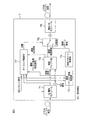
図1は、局側装置OLTと複数の宅側装置ONUとを、光ファイバで接続した光通信システム1の構成例を示す概略図である。
光通信システム1は、制御局側局舎に備えられる局側装置OLT2と、複数の加入者宅に備えられる宅側装置ONU3a,3b,...(以下、総称するときは「宅側装置ONU3」という)と、局側装置OLT2に接続された幹線光ファイバ4a及び各宅側装置ONU3に接続された支線光ファイバ4b(以下、総称するときは「光ファイバ4」という)と、幹線光ファイバ4aと複数の支線光ファイバ4bとを接続するための光カプラ5と、幹線光ファイバ4aの途中に挿入された光信号中継装置7を備えている。
Hereinafter, embodiments of the present invention will be described in detail with reference to the accompanying drawings.
FIG. 1 is a schematic diagram showing a configuration example of an
The
宅側装置ONU3は、各加入者が光ネットワークサービスを享受するための装置であり、加入者宅内に設置されている。宅側装置ONU3は、パーソナルコンピュータ(以下、単にPCという)9などの端末装置に接続される。
光カプラ5は、外部からの電源供給を特に必要とせず、一方に接続された光ファイバ4から入力される信号を、受動的に分岐・多重化して、他方に接続された光ファイバ4に出力することができるスターカプラで形成されている。これにより、1つの局側装置OLT2に対して、多くの宅側装置ONU3を割り当てることができ、全体的な設備コストを抑えることができる。
The home-side device ONU3 is a device for each subscriber to enjoy the optical network service, and is installed in the subscriber's home. The home apparatus ONU 3 is connected to a terminal device such as a personal computer (hereinafter simply referred to as a PC) 9.
The
局側装置OLT2及び宅側装置ONU3を含むこの光通信システム1は、例えば、ギガビットイーサネット(登録商標)(Gigabit Ethernet)技術を取り込み、光ファイバを用いた1.25Gbpsの通信速度のアクセス区間通信を実現するGE−PON(Gigabit Ethernet-Passive Optical Network; IEEE802.3ah)システムを構築している。しかしGE−PONにかぎらず、他のPONシステムを採用することも可能である。例えば、10G−EPON(IEEE802.3av)システムを採用してもよい。
This
このGE−PONシステム又は10G−EPONシステムに従えば、局側装置OLT2と宅側装置ONU3とは、可変長なフレームを単位として、相互の通信を行う。このフレームは、サンプリング・データを含む同期ビット部と、64バイト以上のデータ部とを有している。
以下、宅側装置ONU3と局側装置OLT2との信号の、下り方向と上り方向との信号の送受信手順を説明する。
According to this GE-PON system or 10G-EPON system, the station side device OLT2 and the home side device ONU3 communicate with each other in units of variable length frames. This frame has a synchronization bit portion including sampling data and a data portion of 64 bytes or more.
Hereinafter, a signal transmission / reception procedure in the downlink direction and the uplink direction of the signals between the home-side apparatus ONU3 and the station-side apparatus OLT2 will be described.
まず、インターネット網などの上位のネットワークから宅側装置ONU3へ向けて送られる下り方向の信号の流れを説明する。
上位のネットワークから信号を受け取った局側装置OLT2において、中継されるべき論理リンクを特定するために、所定のブリッジ処理が行われる。このとき、局側装置OLT2は、フレーム信号に、論理リンク識別子を含む同期ビット部やPONヘッダなどの情報を付加し、光信号に変換して、幹線光ファイバ4aに送る。
First, the flow of a downstream signal transmitted from a higher-level network such as the Internet network toward the home apparatus ONU 3 will be described.
In the station side apparatus OLT2 that has received the signal from the upper network, a predetermined bridge process is performed in order to specify the logical link to be relayed. At this time, the station side device OLT2 adds information such as a synchronization bit part including a logical link identifier and a PON header to the frame signal, converts it into an optical signal, and sends it to the trunk
この下りの光信号は、特定の宅側装置ONU3を指定した送信信号と、宅側装置ONU3を指定しないアイドル信号との組み合わせで構成されており、途絶えることのない連続信号となっている。
幹線光ファイバ4aに送られた光信号は、光信号中継装置7を通り、光カプラ5で分岐され、各支線光ファイバ4bを介して、各宅側装置ONU3に送られる。このとき、当該論理リンクを備えている宅側装置ONU3のみが、所定の光信号を取り込むことができる。そして、当該フレーム信号を取り込んだ宅側装置ONU3は、宅内ネットワークインタフェースを中継し、PC9などの端末装置にデータを送る。
This downstream optical signal is composed of a combination of a transmission signal designating a specific home-side device ONU3 and an idle signal not designating the home-side device ONU3, and is a continuous signal that is not interrupted.
The optical signal sent to the trunk
次に、各宅側装置ONU3からインターネット網などの上位のネットワークへ向けて送られる上り方向の信号の流れを説明する。
各PC9からのデータは、各宅側装置ONU3を介して、光バースト信号に変換される。光バースト信号を構成するビットの伝送レートは、例えばGE−PONの場合1.25Gbps、10G−EPONの場合10.3125Gbpsである。
Next, the flow of an upstream signal sent from each home apparatus ONU 3 to a higher-level network such as the Internet network will be described.
Data from each
これらの光バースト信号は各支線光ファイバ4を介して送信され、光カプラ5を介して、幹線光ファイバ4a上をそれぞれの光バースト信号が、多重化されて送られる。
このとき、これらの光バースト信号は、互いに時間的に競合しないように送信されるよう、制御を受ける。この制御は、局側装置OLT2から各宅側装置ONU3へデータを送信するとき、各宅側装置ONU3に対して、上り光信号を送信してもよい期間ウインドウ(以下、単にウインドウともいう)が割り当てられ、制御フレームとして通知されることで行われる。したがって、同一の光通信システム1において、各宅側装置ONU3から送られる上り光信号は、競合を回避することができる。
These optical burst signals are transmitted through the branch optical fibers 4, and the optical burst signals are multiplexed and transmitted through the
At this time, these optical burst signals are controlled to be transmitted so as not to compete with each other in time. In this control, when data is transmitted from the station-side device OLT2 to each home-side device ONU3, there is a period window (hereinafter also simply referred to as a window) in which an upstream optical signal may be transmitted to each home-side device ONU3. Assigned and notified as a control frame. Therefore, in the same
このようにして、宅側装置ONU3と局側装置OLT2との相互の光通信が行われる。
図2は、時分割方式を用いて、各宅側装置ONU3から光ファイバ4を介して局側装置OLT2へ送られる、上り光フレーム信号の光バースト伝送を示す模式図である。
上り光フレーム信号は、宅側装置ONU3aからの光バースト信号6a、宅側装置ONU3bからの光バースト信号6b、宅側装置ONU3cからの光バースト信号6cなどが互いに時間的に競合しないように、ウィンドウによる制御を受けて、送信される。
In this way, mutual optical communication between the home-side apparatus ONU3 and the station-side apparatus OLT2 is performed.
FIG. 2 is a schematic diagram showing optical burst transmission of an upstream optical frame signal transmitted from each home-side apparatus ONU 3 to the station-side apparatus OLT 2 via the optical fiber 4 using a time division method.
The upstream optical frame signal has a window so that the
各宅側装置ONU3からの光バースト信号に含まれる信号は、プリアンブルPAを構成する同期ビット部と、複数のフレームやセルが含まれたデータ部DATAなどの信号とを含む。
同期ビット部は、局側装置OLT2内に備わる光バーストビット同期回路のビット同期確立のために用いられている。同期ビット部のパターンは、GE−PONでは8B10Bのアイドル信号となっている。そのマーク率(0,1の比率)は通常50%、ビット数は固定となっている。10G−EPONでは固定の66ビットの同期パターンの繰り返し信号となっている。そのマーク率は、同期ビット部においては、通常50%、ビット数は固定となっている。
The signal included in the optical burst signal from each home-side apparatus ONU3 includes a synchronization bit portion that constitutes the preamble PA and a signal such as a data portion DATA that includes a plurality of frames and cells.
The synchronization bit part is used for bit synchronization establishment of an optical burst bit synchronization circuit provided in the station side apparatus OLT2. The pattern of the synchronization bit part is an 8B10B idle signal in GE-PON. The mark ratio (ratio of 0, 1) is usually 50%, and the number of bits is fixed. In 10G-EPON, a repetitive signal of a fixed 66-bit synchronization pattern is used. The mark rate is usually 50% in the synchronous bit part, and the number of bits is fixed.
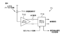
図3は、本発明の光信号中継装置7の構成を示すブロック図であり、図4、図5は、その中の光/電気モジュール71の細部を示す。図6は、光信号中継装置7内の各部の信号波形図である。
光信号中継装置7は、光バースト信号をバースト受信信号(バースト受信信号という;図6(a)参照)に変換し、光信号に戻して中継する装置である。
FIG. 3 is a block diagram showing the configuration of the
The optical
本実施の形態では、光信号中継装置7は、双方向の光信号中継装置7であって、一方が宅側装置ONUから局側装置OLTへの上りの光バースト信号を中継し、他方が局側装置OLTから宅側装置ONUへの下りの光連続信号を中継する。
上りの光バースト信号を中継する光信号中継装置7は、図3に示すように、光バースト信号をバースト受信信号に変換する光/電気モジュール71と、光バースト信号の受信開始/受信終了を検出することのできるタイミング制御部77とを備えている。
In the present embodiment, the
As shown in FIG. 3, the
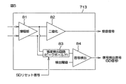
光/電気モジュール71は、図4に示すように、光/電気変換素子711と、光/電気変換素子711による光検出信号(バースト受信信号という)を増幅するプリアンプ712と、プリアンプ712の出力に対してキャパシタを介してAC結合されプリアンプ712の出力信号をさらに増幅するポストアンプ713とを備えている。
ポストアンプ713は、図5に示すように、プリアンプ712の出力信号を増幅する増幅部81と、バースト受信信号を所定の閾値を用いて二値化する二値化部82とを備えている。ポストアンプ713は、さらにバースト受信信号が存在しているかどうかを検出するためのピークホールド回路83(強度検出回路)と、信号検出部84とを備えている。信号検出部84は、ピークホールド回路83の出力を検出閾値と比較し、ピークホールド回路83の出力が検出閾値を超えている時間だけ、SD信号(図6(b)参照)を出力する。
As shown in FIG. 4, the optical /
As shown in FIG. 5, the
ピークホールド回路83は、タイミング制御部77からSDリセット信号(図6(c)参照)を受け入れる。このSDリセット信号は、タイミング制御部77がバースト受信信号をモニタし、例えば、バースト受信信号の二値のうち”0”が所定時間続いたことを検出した場合に、バースト受信信号が終了したと判断し、ピークホールド回路83に送る信号(SDリセット信号)である。このSDリセット信号の時間をリセット時間Trstという。リセット時間Trstは、光信号中継装置7で設定される時間であり、リセット時間Trstが短かすぎると、SDリセット信号でピークホールド回路83をリセットしても、前段にあるプリアンプ712や交流結合回路(AC結合)に電荷が残っているため、残った電荷が次のバースト信号と誤検出されてしまうおそれがある。
The
またリセット時間Trstは、PONシステムで使われる最小のバースト信号長より短く設定することが好ましい。最小のバースト信号以上に設定すると、連続バースト受信判定を出力する場合、リセット時間内に、光信号中継装置7を通らないONU(例えば図1に示すONU3d)が送信する次のバースト信号が重なるおそれがあるからである。バースト信号長より短く設定することにより、このような次のバースト信号と衝突しないことが保証される。
The reset time Trst is preferably set shorter than the minimum burst signal length used in the PON system. If the burst signal is set to be equal to or greater than the minimum burst signal, the next burst signal transmitted by an ONU that does not pass through the optical signal repeater 7 (for example,
図3を参照して、光/電気モジュール71は、光バースト信号有りの状態を示す信号検出信号(SD信号)をタイミング制御部77に供給する。タイミング制御部77は、このSD信号をもとに光バースト信号の受信開始を知ることができる。また、タイミング制御部77は光/電気モジュール71の出力をモニタして受信終了を知ることができる。受信終了を検知した時、前述したように、SDリセット信号を光/電気モジュール71に供給する。
Referring to FIG. 3, the optical /
本発明の実施形態では、連続バースト受信判定部72を設けている。この連続バースト受信判定部72は、SD信号とSDリセット信号とを入力して、ひとつのSD信号が終了し、前記リセット時間Trstの経過した時点で、次のSD信号が検出されていると判定した場合、所定の時間にわたって、連続バースト受信判定信号をタイミング制御部77に出力する回路である。ひとつのSD信号が終了し、前記リセット時間Trstの経過後、次のSD信号が検出されていない場合には、前記連続バースト受信判定信号を出力しない。
In the embodiment of the present invention, a continuous burst
「前記リセット時間Trstの経過後、次のSD信号が検出されている」ならば、ひとつのバースト受信信号が終了し、前記リセット時間Trstが経過する前に、すでに次のバースト受信信号が入ってきている。つまり、隣接する上りの光バースト信号が、ほぼ連続した状態で光信号中継装置7に入ってきている、ということである。連続バースト受信判定部72は、このような、上りの光バースト信号の連続受信状態を判定する。
If “the next SD signal is detected after the lapse of the reset time Trst”, one burst reception signal is completed, and the next burst reception signal has already entered before the reset time Trst has elapsed. ing. That is, the adjacent upstream optical burst signal enters the
連続バースト受信判定信号の継続期間は、前記リセット時間Trstの経過時点を0とすると、時点T1からT2までである(図6(d)参照)。T2−T1は、0<(T2−T1)<Trstを満たす値に設定される。T2は、Trst以上、1つの光バースト信号の中の同期ビット部が続く時間以下の値に設定される。
0でないT1を設ける意味は、光信号中継装置7から出力される隣接するバースト信号間に、最小のバースト間隔を確保するためである。T2はTrstに等しいか、それよりも長い値に設定するとよい(図6(d)では、T2=Trstの場合が例示されている)。
The duration of the continuous burst reception determination signal is from time T1 to time T2 when the elapsed time of the reset time Trst is 0 (see FIG. 6D). T2-T1 is set to a value satisfying 0 <(T2-T1) <Trst. T2 is set to a value equal to or greater than Trst and equal to or less than the time that the synchronization bit portion in one optical burst signal continues.
The meaning of providing T1 which is not 0 is to secure a minimum burst interval between adjacent burst signals output from the
光/電気モジュール71で変換されたバースト受信信号は、クロック再生部(図示せず)に入力される。クロック再生部は、光バースト信号に基づいて、光バースト信号の各ビットに同期したクロック信号を抽出する。この信号を「再生クロック」という。そして再生クロックによってバースト受信信号の各ビットをサンプリングして遅延バッファ部73に書き込む。
The burst reception signal converted by the optical /
遅延バッファ部73は遅延時間に応じた深さを持つFIFOメモリで構成され、光信号中継装置7の基準クロックで読み出す。基準クロックには、局側端局装置OLT2から子局ONU3への下り信号を中継する際に抽出した再生クロックを用いることができる。
なお、再生クロックを用いず、外部から基準クロックを入力して、その基準クロックに基づいて時間管理することとしてもよい。
The
Instead of using the recovered clock, a reference clock may be input from the outside and time management may be performed based on the reference clock.
図6(e)は遅延バッファ部73に書き込まれる前のバースト受信信号を示し、図6(f)は、遅延バッファ部73に書き込まれた後のバースト受信信号を示す。遅延バッファ部73の中の遅延時間Tdelayは、Trstに等しいか又はそれ以上の値に設定するとよい(図6(f)では、T2=Trstの場合が例示されている)。遅延時間Tdelayの設定の上限は、1つの光バースト信号の中で同期ビット部が続く時間である。
FIG. 6E shows a burst reception signal before being written to the
切替部75は、同期パターン保持部74から出力される同期パターン信号と、遅延バッファ部73から出力されるバースト受信信号とを、タイミング制御部77からの切替信号に基づいて切り替える。
本発明のひとつの実施形態では、タイミング制御部77は、連続バースト受信判定信号が継続している期間中(図6(d)参照)、切替部75に切替え信号を送り、遅延されたバースト受信信号を、同期パターン信号に切替えさせる。したがって遅延されたバースト受信信号が、同期パターン信号で置き換えられる。この置き換えにより、「次のバースト受信信号」に対して、最小のバースト間隔を設けた上で、リセット信号期間中に受信することができなかったバースト受信信号の最初の部分を補完することができる。
The switching
In one embodiment of the present invention, the
本発明の他の実施形態では、バースト受信信号だけでなく、SD信号も遅延バッファ部73に送り込み、遅延バッファ部73から、遅延されたバースト受信信号とSD信号とを取り出す。バースト受信信号とSD信号の遅延時間は、ともに同じ時間であってもよい。
この場合、遅延されたSD信号の波形を図6(g)に示す。タイミング制御部77は、連続バースト受信判定信号が継続している期間中(図6(d)参照)と、遅延されたSD信号が継続している期間中(図6(g)参照)との論理和(図6(h)参照)をとり、その論理和に基づいて、切替部75に切替え信号を送り、遅延されたバースト受信信号を、同期パターン信号に切替えさせる。
In another embodiment of the present invention, not only the burst reception signal but also the SD signal is sent to the
In this case, the waveform of the delayed SD signal is shown in FIG. The
なお、タイミング制御部77は、論理和が続いている期間中、切替部75に切替え信号を送り続けることとすれば、データ部分も同期パターンに置き換えてしまうおそれがあるので、プリアンブル時間内で切り替えを解除するようにしている。
この「他の実施形態」では、「次のバースト受信信号」に対して、最小のバースト間隔を設けた上で、リセット時間のためにSD信号が発生しなかった同期パターンの前の部分と、リセット時間が過ぎてSD信号が発生した同期パターンの後の部分とのいずれも、同期パターン信号で置き換えることができる。
Note that if the
In this “other embodiment”, with respect to the “next burst reception signal”, a minimum burst interval is provided, and the previous part of the synchronization pattern in which the SD signal is not generated due to the reset time; Any part of the latter part of the synchronization pattern in which the SD signal is generated after the reset time has passed can be replaced with the synchronization pattern signal.
なおいずれの実施形態でも、前述したように、遅延バッファ部73と同期パターン保持部74とは再生クロック若しくは基準クロックで同期されており、切替え制御も再生クロック若しくは基準クロックで同期させることで、切替による周波数変動や位相変動は発生しない。なお、切替時に同期パターンが壊れる可能性があるが、せいぜい切り替えた1ビットの前後に限定されるので、周波数変動/位相変動は発生せず、マーク率も大きく変動することはなく、局側装置OLTの受信に影響を及ぼすことはない。
In any embodiment, as described above, the
電気/光モジュール76は、このようにして同期ビット部の先頭が正しい同期パターンに置換された復元信号を、光バースト信号に変換する(図6(j)参照)。
以上のようにして、光バースト信号を、その正確な符号形態を保ったまま中継することができる。
なお、ひとつのSD信号が終了し、次のSD信号が前記リセット時間Trstの経過時点よりも遅く入ってきた場合、つまり光バースト信号が連続して入ってこない場合の処理を、図6を用いて説明する。
The electrical /
As described above, the optical burst signal can be relayed while maintaining its accurate code form.
The process when one SD signal ends and the next SD signal enters later than the time when the reset time Trst has elapsed, that is, when the optical burst signal does not continuously enter is shown in FIG. I will explain.
この場合、バースト受信信号を遅延させることはいままで説明したとおりであるが、連続バースト受信判定信号は発生しない(図6(d)の左の部分を参照)。したがって、遅延されたSD信号(図6(h)参照)に基づいて切替部75に切替え信号を送り、遅延されたバースト受信信号の先頭部分を同期パターン信号に切替えさせる。この処理によって、損傷しているかもしれないバースト受信信号の始めの部分を同期パターン信号で置き換えることができる。なお、バースト信号が連続していない場合にSD信号が検出される前の部分を補完して中継すると、中継装置よりも局側装置(OLT)側でバースト信号が衝突してしまうおそれがある。例えば、図3の場合、中継装置7からの中継信号と子局ONU3dからのバースト信号6dと衝突する可能性があり、この衝突を回避することができる。
In this case, the burst reception signal is delayed as described above, but the continuous burst reception determination signal is not generated (see the left part of FIG. 6D). Therefore, a switching signal is sent to the
以上で、本発明の実施形態を説明したが、本発明の実施は、前記に限定されるものではなく、本発明の範囲で種々の変更を施すことが可能である。
本発明の権利範囲は、特許請求の範囲によって示され、特許請求の範囲と均等の意味及び範囲内でのすべての変更が含まれることが意図されている。
Although the embodiment of the present invention has been described above, the implementation of the present invention is not limited to the above, and various modifications can be made within the scope of the present invention.
The scope of the present invention is defined by the terms of the claims, and is intended to include any modifications within the scope and meaning equivalent to the terms of the claims.
1 光通信システム
7 光信号中継装置
71 光/電気モジュール
72 連続バースト受信判定部
73 遅延バッファ部
74 同期パターン保持部
75 切替部
76 電気/光モジュール
77 タイミング制御部
84 信号検出部
DESCRIPTION OF
Claims (7)
受信した光バースト信号をバースト受信信号に変換する光/電気変換モジュールと、
前記光/電気変換モジュールにより変換された前記バースト受信信号を検出している期間中、SD信号を出力する信号検出部であって、ひとつのバースト受信信号の終了を検出すれば、所定のリセット時間が経過した後、次のバースト受信信号の検出を始める前記信号検出部と、
前記光/電気モジュールから出力される前記バースト受信信号を蓄積して遅延させ、当該遅延されたバースト受信信号を出力する遅延バッファ部と、
光バースト信号の同期パターンを、同期パターン信号として保持している同期パターン保持部と、
前記遅延バッファ部から出力される遅延されたバースト受信信号と、前記同期パターン保持部が保持している同期パターン信号との切替を行う切替部と、
前記切替部の切替えを制御するタイミング制御部と、
前記切替部によって切替えられた出力信号を、光バースト信号に変換する電気/光変換器とを備え、
前記信号検出部の出力を監視し、ひとつのSD信号の終了後、次のSD信号が前記リセット時間経過時に検出されていると判定した場合、所定の時間にわたって、連続バースト受信判定信号を出力する連続バースト信号受信判定部をさらに備え、
前記タイミング制御部は、前記連続バースト受信判定信号が存在する期間にわたって、前記バッファ部から出力される遅延されたバースト受信信号の同期パターンを、前記同期パターン信号に切り替えるように前記切替部を制御するものである、光信号中継装置。 An optical signal repeater that relays an optical burst signal,
An optical / electrical conversion module for converting a received optical burst signal into a burst received signal;
During detection of the burst reception signal converted by the optical / electrical conversion module, a signal detection unit that outputs an SD signal, and detects the end of one burst reception signal, a predetermined reset time After the elapse of time, the signal detector that starts detection of the next burst received signal,
A delay buffer unit that accumulates and delays the burst reception signal output from the optical / electrical module, and outputs the delayed burst reception signal;
A synchronization pattern holding unit holding the synchronization pattern of the optical burst signal as a synchronization pattern signal;
A switching unit for switching between the delayed burst reception signal output from the delay buffer unit and the synchronization pattern signal held by the synchronization pattern holding unit;
A timing control unit for controlling switching of the switching unit;
An electrical / optical converter that converts the output signal switched by the switching unit into an optical burst signal;
The output of the signal detector is monitored, and after the end of one SD signal, if it is determined that the next SD signal is detected when the reset time has elapsed, a continuous burst reception determination signal is output for a predetermined time. Further comprising a continuous burst signal reception determination unit,
The timing control unit controls the switching unit to switch a synchronization pattern of a delayed burst reception signal output from the buffer unit to the synchronization pattern signal over a period in which the continuous burst reception determination signal exists. An optical signal relay device.
前記切替部は、前記遅延されたSD信号が存在する期間と、前記連続バースト受信判定信号が存在する期間の両方にわたって、前記バッファ部から出力される遅延されたバースト受信信号を、前記同期パターン信号に切り替えるものである、請求項1又は請求項2に記載の光信号中継装置。 The delay buffer unit further accumulates and delays the SD signal output from the signal detection unit, and outputs the delayed SD signal.
The switching unit converts the delayed burst reception signal output from the buffer unit to the synchronization pattern signal over both a period in which the delayed SD signal exists and a period in which the continuous burst reception determination signal exists. The optical signal repeater according to claim 1, wherein the optical signal repeater is switched to
受信した光バースト信号をバースト受信信号に変換し、
前記変換されたバースト受信信号を検出し、ひとつのバースト受信信号の終了を検出すれば、所定のリセット時間が経過した後、次のバースト受信信号の検出を始め、その検出している期間中、SD信号を出力し、
前記変換されたバースト受信信号を蓄積して遅延させ、
前記光バースト信号の同期パターンを、同期パターン信号として保持し、
前記遅延されたバースト受信信号と、前記保持している同期パターン信号との切替を行い、
前記切替えられた出力信号を光バースト信号に変換する、中継方法であって、
前記信号検出部の出力を監視し、ひとつのSD信号の終了後、次のSD信号が前記リセット時間経過時に検出されたと判定した場合、所定の時間にわたって、連続バースト受信判定信号を出力し、
前記連続バースト受信判定信号が存在する期間にわたって、前記バッファ部から出力される遅延されたバースト受信信号の同期パターンを、前記同期パターン信号に切り替える、中継方法。 An optical signal relay method for relaying an optical burst signal,
Convert received optical burst signal to burst received signal,
If the converted burst reception signal is detected and the end of one burst reception signal is detected, the detection of the next burst reception signal is started after a predetermined reset time has elapsed, during the period of detection, Output SD signal,
Accumulating and delaying the converted burst received signal,
Holding the synchronization pattern of the optical burst signal as a synchronization pattern signal;
Switching between the delayed burst reception signal and the held synchronization pattern signal,
A relay method for converting the switched output signal into an optical burst signal,
When monitoring the output of the signal detector and determining that the next SD signal has been detected when the reset time has elapsed after the end of one SD signal, a continuous burst reception determination signal is output for a predetermined time;
A relay method, wherein a synchronization pattern of a delayed burst reception signal output from the buffer unit is switched to the synchronization pattern signal over a period in which the continuous burst reception determination signal exists.
Priority Applications (2)
| Application Number | Priority Date | Filing Date | Title |
|---|---|---|---|
| JP2016079903A JP2017192002A (en) | 2016-04-12 | 2016-04-12 | Optical signal relay device and relay method |
| PCT/JP2016/087392 WO2017179241A1 (en) | 2016-04-12 | 2016-12-15 | Optical signal relay apparatus and relay method |
Applications Claiming Priority (1)
| Application Number | Priority Date | Filing Date | Title |
|---|---|---|---|
| JP2016079903A JP2017192002A (en) | 2016-04-12 | 2016-04-12 | Optical signal relay device and relay method |
Publications (1)
| Publication Number | Publication Date |
|---|---|
| JP2017192002A true JP2017192002A (en) | 2017-10-19 |
Family
ID=60041622
Family Applications (1)
| Application Number | Title | Priority Date | Filing Date |
|---|---|---|---|
| JP2016079903A Pending JP2017192002A (en) | 2016-04-12 | 2016-04-12 | Optical signal relay device and relay method |
Country Status (2)
| Country | Link |
|---|---|
| JP (1) | JP2017192002A (en) |
| WO (1) | WO2017179241A1 (en) |
Cited By (2)
| Publication number | Priority date | Publication date | Assignee | Title |
|---|---|---|---|---|
| WO2020250770A1 (en) * | 2019-06-11 | 2020-12-17 | 富士フイルム株式会社 | Microneedle array unit and container |
| JP2023119083A (en) * | 2022-02-16 | 2023-08-28 | 三菱電機株式会社 | Optical communication device |
Family Cites Families (4)
| Publication number | Priority date | Publication date | Assignee | Title |
|---|---|---|---|---|
| JP2002271271A (en) * | 2001-03-06 | 2002-09-20 | Hitachi Ltd | Reproduction relay method and reproduction relay device |
| JP4072184B2 (en) * | 2005-12-09 | 2008-04-09 | 古河電気工業株式会社 | Optical transmission system |
| JP4761135B2 (en) * | 2006-02-20 | 2011-08-31 | 住友電気工業株式会社 | Optical signal relay device and relay method |
| CN101364844B (en) * | 2007-08-10 | 2011-03-30 | 华为技术有限公司 | Device for realizing remote data transmission in passive optical network |
-
2016
- 2016-04-12 JP JP2016079903A patent/JP2017192002A/en active Pending
- 2016-12-15 WO PCT/JP2016/087392 patent/WO2017179241A1/en not_active Ceased
Cited By (2)
| Publication number | Priority date | Publication date | Assignee | Title |
|---|---|---|---|---|
| WO2020250770A1 (en) * | 2019-06-11 | 2020-12-17 | 富士フイルム株式会社 | Microneedle array unit and container |
| JP2023119083A (en) * | 2022-02-16 | 2023-08-28 | 三菱電機株式会社 | Optical communication device |
Also Published As
| Publication number | Publication date |
|---|---|
| WO2017179241A1 (en) | 2017-10-19 |
Similar Documents
| Publication | Publication Date | Title |
|---|---|---|
| CN101162941B (en) | Apparatus of adjusting optical signal transmission timing | |
| JP4340692B2 (en) | Passive optical network system and operation method thereof | |
| JP5842438B2 (en) | Relay device, relay method, and optical transmission system | |
| EP2326104A2 (en) | Terminal apparatus, data transmission system and data transmission method | |
| US10484096B2 (en) | Relay apparatus and relay method for passive optical network | |
| EP2395725B1 (en) | Method for burst transmission on a passive optical network and device for receiver resetting | |
| CN101729154B (en) | Method, device and system for realizing LR-PON | |
| US9287981B2 (en) | Station-side apparatus and PON system | |
| CN101577590B (en) | Signal transmission method, relay device and passive optical network system | |
| JP4911358B2 (en) | Optical burst signal repeater and optical communication system | |
| JP2017192002A (en) | Optical signal relay device and relay method | |
| CN101478701A (en) | Control method and apparatus for uplink data transmission | |
| JP5105138B2 (en) | Optical signal repeater and optical communication system | |
| JP4761135B2 (en) | Optical signal relay device and relay method | |
| JP5084629B2 (en) | Subscriber termination device and power supply control method | |
| JP4893589B2 (en) | PON system station side apparatus and frame processing method | |
| KR101294516B1 (en) | Method and apparatus for burst mode clock and data recovery | |
| JP5420435B2 (en) | Station side equipment | |
| JP5365887B2 (en) | Optical signal repeater and optical communication system | |
| JP5411805B2 (en) | Passive optical network system, transmission light control method, optical multiple termination device, and optical network termination device | |
| KR101586075B1 (en) | Passive optical network relaying system for extending transmission distance and method thereof | |
| JP5684344B2 (en) | Station side equipment | |
| JP5965427B2 (en) | Optical signal relay device, monitoring control device, communication control method, and communication control program | |
| JP2016015640A (en) | Received signal processing apparatus, optical signal repeater using the same, and optical signal repeater | |
| JP5992799B2 (en) | Receiving apparatus, communication system, program, and method for acquiring transmission side information using differentiating means |
Legal Events
| Date | Code | Title | Description |
|---|---|---|---|
| A621 | Written request for application examination |
Free format text: JAPANESE INTERMEDIATE CODE: A621 Effective date: 20181022 |
|
| A131 | Notification of reasons for refusal |
Free format text: JAPANESE INTERMEDIATE CODE: A131 Effective date: 20191121 |
|
| A02 | Decision of refusal |
Free format text: JAPANESE INTERMEDIATE CODE: A02 Effective date: 20200618 |