JP2017143433A - Communication system and communication method - Google Patents
Communication system and communication method Download PDFInfo
- Publication number
- JP2017143433A JP2017143433A JP2016023958A JP2016023958A JP2017143433A JP 2017143433 A JP2017143433 A JP 2017143433A JP 2016023958 A JP2016023958 A JP 2016023958A JP 2016023958 A JP2016023958 A JP 2016023958A JP 2017143433 A JP2017143433 A JP 2017143433A
- Authority
- JP
- Japan
- Prior art keywords
- phase
- sub
- signal
- spectrums
- frequency
- Prior art date
- Legal status (The legal status is an assumption and is not a legal conclusion. Google has not performed a legal analysis and makes no representation as to the accuracy of the status listed.)
- Granted
Links
- 238000000034 method Methods 0.000 title claims abstract description 74
- 238000004891 communication Methods 0.000 title claims description 33
- 230000005540 biological transmission Effects 0.000 claims abstract description 101
- 230000010363 phase shift Effects 0.000 claims abstract description 77
- 230000002123 temporal effect Effects 0.000 claims abstract description 13
- 238000001228 spectrum Methods 0.000 claims description 185
- 238000009499 grossing Methods 0.000 claims description 94
- 230000008569 process Effects 0.000 claims description 48
- 230000007704 transition Effects 0.000 claims description 36
- 238000012545 processing Methods 0.000 claims description 29
- 239000006185 dispersion Substances 0.000 claims description 17
- 238000012937 correction Methods 0.000 claims description 13
- 238000000605 extraction Methods 0.000 claims description 13
- 238000000819 phase cycle Methods 0.000 description 43
- 238000004364 calculation method Methods 0.000 description 21
- RDYMFSUJUZBWLH-UHFFFAOYSA-N endosulfan Chemical compound C12COS(=O)OCC2C2(Cl)C(Cl)=C(Cl)C1(Cl)C2(Cl)Cl RDYMFSUJUZBWLH-UHFFFAOYSA-N 0.000 description 9
- 238000007493 shaping process Methods 0.000 description 8
- 239000000284 extract Substances 0.000 description 6
- 238000004088 simulation Methods 0.000 description 6
- 230000000052 comparative effect Effects 0.000 description 4
- 230000007423 decrease Effects 0.000 description 4
- 238000005094 computer simulation Methods 0.000 description 3
- 230000000694 effects Effects 0.000 description 3
- 238000005562 fading Methods 0.000 description 3
- 230000003247 decreasing effect Effects 0.000 description 2
- 230000009467 reduction Effects 0.000 description 2
- 238000013459 approach Methods 0.000 description 1
- 230000015556 catabolic process Effects 0.000 description 1
- 230000008859 change Effects 0.000 description 1
- 230000000295 complement effect Effects 0.000 description 1
- 238000007796 conventional method Methods 0.000 description 1
- 230000001186 cumulative effect Effects 0.000 description 1
- 238000006731 degradation reaction Methods 0.000 description 1
- 238000010586 diagram Methods 0.000 description 1
- 238000005315 distribution function Methods 0.000 description 1
- 125000002924 primary amino group Chemical group [H]N([H])* 0.000 description 1
- 229940035637 spectrum-4 Drugs 0.000 description 1
Images


Landscapes
- Digital Transmission Methods That Use Modulated Carrier Waves (AREA)
Abstract
Description
本発明は、帯域分散伝送方式を用いた通信技術に関する。 The present invention relates to a communication technique using a band dispersion transmission system.
近年、通信システムにおける周波数帯域の利用効率を向上するために、送信側において、シングルキャリア変調信号を周波数領域で複数のサブスペクトラムに分割し、サブスペクトラムを分散配置する帯域分散伝送方式が考えられている。帯域分散伝送方式は、スペクトラムを分割して分散配置するため、送信信号のピーク対平均電力比(PAPR:Peak to Average Power Ratio)が増大するという問題があり、PAPRを低減する技術が検討されている(例えば、非特許文献1参照)。ここで、帯域分散伝送方式を用いる通信においてPAPRを低減する技術について説明する。 In recent years, in order to improve the efficiency of using frequency bands in communication systems, there has been considered a band dispersion transmission method in which a single carrier modulation signal is divided into a plurality of sub-spectrums in the frequency domain and the sub-spectrums are distributed. Yes. In the band dispersion transmission method, since the spectrum is divided and distributed, there is a problem that the peak to average power ratio (PAPR) of the transmission signal increases, and a technique for reducing the PAPR has been studied. (For example, refer nonpatent literature 1). Here, a technique for reducing PAPR in communication using a band dispersion transmission scheme will be described.
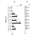
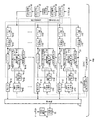
図15は、帯域分散伝送方式を用いる送信装置150の一例を示す。図15において、送信装置150は、変調回路101、波形整形フィルタ102、DFT(Discrete Fourier Transform)回路103、分割フィルタ104−1〜104−ND、位相器105−1−1〜105−C−ND、周波数シフタ106−1−1〜106−C−ND、加算器107−1〜107−C、IDFT(Inverse DFT)回路108−1〜108−C、PAPR算出回路109−1〜109−C,最小PAPR信号選択器110および位相系列制御装置151を備える。ここで、NDおよびCは正の整数である。
FIG. 15 shows an example of a
変調回路101は、送信データを例えばQPSK(Quadrature Phase Shift Keying)などの変調方式で変調する。
The
波形整形フィルタ102は、変調回路101が出力する変調信号の帯域を制限するためのフィルタである。
The
DFT回路103は、波形整形フィルタ102から出力される変調信号を所定のDFT区間ごとに逐次周波数領域(スペクトラム)の信号に変換する。ここで、DFT区間を処理時刻が早いものから順に“1番目のDFT区間”,“2番目のDFT区間”,…,“t番目のDFT区間”,…,“t+u番目のDFT区間”,…と称する。なお、t,uは正の整数である。
The
分割フィルタ104−k(1≦k≦ND)は、DFT回路103が周波数領域に変換した変調信号の帯域をND個に分割するためのフィルタである。例えば、周波数領域に変換された各DFT区間の変調信号は、分割フィルタ104−1〜104−NDにより、ND個のサブ変調信号(サブスペクトラム)に分割される。ここで、処理時刻が早いものから順に“1番目のDFT区間のサブスペクトラム”,“2番目のDFT区間のサブスペクトラム”,…,“t番目のDFT区間のサブスペクトラム”,…,“t+u番目のDFT区間のサブスペクトラム”,…と称する。各分割フィルタ104−kの出力信号は、C個に分岐され、1番目からC番目までの分岐信号が位相器105−q−k(1≦q≦C、1≦k≦ND)にそれぞれ出力される。ここで、q,k,Cは正の整数である。
The division filter 104-k (1 ≦ k ≦ N D ) is a filter for dividing the band of the modulation signal converted into the frequency domain by the
図16(a)は、分割フィルタ104に入力する前のスペクトラムの一例を示し、図16(b)は、ND=4の場合に各分割フィルタから出力されるサブスペクトラムの一例を示す。
FIG. 16A shows an example of a spectrum before being input to the
位相器105−q−k(1≦q≦C、1≦k≦ND)は、C個に分岐された分割フィルタ104−kの出力信号に予め決められた位相を加算する。位相器105−q−kでは、式(1)で示す位相系列Θ2,Θ3,…,Θq,…,ΘCを用いて、位相器105−q−kに入力された各サブスペクトラムの位相をシフトする(図16(c))。ここで、位相系列制御装置151は、位相系列Θ2,Θ3,…,Θq,…,ΘCを出力する。なお、位相系列Θ2,Θ3,…,Θq,…,ΘCの情報は、受信装置260と共有される。
The phase shifter 105-q-k (1 ≦ q ≦ C, 1 ≦ k ≦ N D ) adds a predetermined phase to the output signal of the C divided filters 104-k. The phase shifter 105-q-k, the phase sequence theta 2 represented by the formula (1), Θ 3, ... , Θ q, ..., using a theta C, each sub-spectrum input to the phase shifter 105-q-k Is shifted (FIG. 16C). The
ここで、位相器105−q−kに入力されるt番目のDFT区間のサブスペクトラムをSStkとする。そして、位相器105−q−kは、式(2)で示す位相系列Θqの位相により、式(3)で示すt番目のDFT区間(t)のサブスペクトラムSStkの位相シフトを行う。 Here, the sub-spectrum of the t-th DFT interval input to the phase shifter 105-q-k is SS tk . Then, the phase shifter 105-q-k performs the phase shift of the sub-spectrum SS tk in the t-th DFT section (t) shown in Expression (3) based on the phase of the phase sequence Θ q shown in Expression (2).
![]()
![]()
位相乗算後の位相器105−q−kの出力信号Sθ tqは式(4)となる。
![]()
![]()
次に、周波数シフタ106−1−k(1≦q≦C、1≦k≦ND)は、各サブスペクトラムを周波数軸上の所望の帯域に分散配置する。 Next, the frequency shifter 106-1-k (1 ≦ q ≦ C, 1 ≦ k ≦ N D ) disperses each sub-spectrum in a desired band on the frequency axis.
加算器107−q(1≦q≦C)は、周波数シフタ106−q−kの出力信号を各組毎(同じq毎)にそれぞれND個のサブスペクトラムを加算する。ここで、ND=4の場合の加算器107−qの出力信号の一例を図16(d)に示す。 The adder 107-q (1 ≦ q ≦ C) adds the N D sub spectrum respective output signals of the frequency shifters 106-q-k for each set (each equivalent q). Here, FIG. 16D shows an example of the output signal of the adder 107-q when N D = 4.
IDFT108−q(1≦q≦C)は、加算器107−qの出力信号を周波数領域の信号から時間領域の信号に変換する。 IDFT 108-q (1 ≦ q ≦ C) converts the output signal of adder 107-q from a frequency domain signal to a time domain signal.
PAPR算出回路109−q(1≦q≦C)は、IDFT108−qで変換された時間領域の信号についてPAPRを算出する。例えば、PAPR算出回路109−qは、IDFT108−qが出力する1番目のDFT区間に対応する信号を入力してPAPRを算出し、最小PAPR信号選択器110に出力する。以降、2番目のDFT区間,…,t番目のDFT区間,…,t+u番目のDFT区間,…についても、1番目のDFT区間と同様に対応する信号のPAPRを算出し、最小PAPR信号選択器110に出力する。
The PAPR calculation circuit 109-q (1 ≦ q ≦ C) calculates the PAPR for the time domain signal converted by the IDFT 108-q. For example, the PAPR calculation circuit 109-q calculates a PAPR by inputting a signal corresponding to the first DFT interval output from the IDFT 108-q and outputs the PAPR to the minimum
最小PAPR信号選択器110は、PAPR算出回路109−qが算出したPAPRのうち最も小さいPAPRの信号をDFT区間ごとに選択して送信する。例えば、最小PAPR信号選択器110は、C=2のPAPR算出回路109−2が算出したPAPRが最も小さい場合、同じ系列(C=2)のIDFT108−2の出力信号を選択して送信する。
The minimum
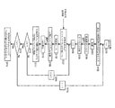
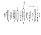
図17は、帯域分散伝送方式を用いる受信装置260の一例を示す。図17において、受信装置260は、DFT回路211、抽出フィルタ212−1〜212−ND、周波数シフタ213−1〜213−ND、位相推定器214−2〜214−ND、位相器215−2〜215−ND、加算器216、IDFT回路217および復調回路218を備える。
FIG. 17 shows an example of a receiving
DFT回路211は、受信信号を周波数領域の信号に変換する。
The
抽出フィルタ212−k(1≦k≦ND)は、ND個に分岐されたDFT回路211の出力信号をそれぞれ入力し、ND個のサブスペクトラムを抽出する。
Extraction filter 212-k (1 ≦ k ≦ N D) is the output signal of the
周波数シフタ213−k(1≦k≦ND)は、抽出フィルタ212−1〜212−NDが出力する各サブスペクトラムを送信装置150の周波数シフタ106−q−1〜106−q−NDで周波数シフトする前の帯域へ戻すように周波数をシフトする。
Frequency shifter 213-k (1 ≦ k ≦ N D) , the extraction filter 212-1 to 212-N D frequency of the
位相推定器214−k(2≦k≦ND)は、周波数シフタ213−1〜213−NDのうち隣接するサブスペクトラムの信号の位相差を推定する。図17において、例えば、位相推定器214−2は、周波数シフタ213−1と周波数シフタ213−2とのそれぞれの出力信号を入力し、送信装置150の位相器105−q−2で位相シフトした位相差を推定する。
Phase estimator 214-k (2 ≦ k ≦ N D) estimates the phase difference of the sub-spectrum of a signal that adjacent ones of the frequency shifter 213-1~213-N D. In FIG. 17, for example, the phase estimator 214-2 receives the output signals of the frequency shifter 213-1 and the frequency shifter 213-2, and is phase-shifted by the phase shifter 105-q-2 of the
位相器215−k(2≦k≦ND)は、位相推定器214−2〜214−NDがそれぞれ出力する信号により、サブスペクトラムSStqkの位相を補償する。例えば、位相器215−2は、位相推定器214−2の出力信号により、サブスペクトラムSStq2の位相を補償する。 Phaser 215-k (2 ≦ k ≦ N D) is the signal phase estimator 214-2~214-N D respectively output to compensate for the phase of the sub-spectrum SS tqk. For example, the phase shifter 215-2 compensates for the phase of the sub-spectrum SS tq2 based on the output signal of the phase estimator 214-2.
加算器216は、周波数シフタ213−1および位相器215−2〜位相器215−NDのそれぞれの出力信号を加算し、送信装置150で複数のサブスペクトラムに分割する前の信号波形に戻す。
The
IDFT回路217は、加算器216の出力信号を入力して時間領域の信号に変換する。
The
復調回路218は、IDFT回路217が出力する変調信号を復調する。例えば、送信装置150の変調回路101がQPSKで変調した場合は、同じQPSKで受信データを復調する。
The
ここで、受信装置260の位相推定器214−kでは、周波数領域で隣接するサブスペクトラム(SStqk−1とSStqk)が入力され、SStqk−1とSStqkとの遷移域における位相差Rtqkを計算する。なお、図16(a)に示すように、送信装置150における各サブスペクトラムの遷移域同士は重畳しているため、隣接するサブスペクトラムの遷移域は同一の信号成分を有している。ここで、重畳している遷移域を重畳領域と称する。受信装置260では、この重畳領域の信号成分から位相差(位相シフト量)Rtqkを推定する。例えば、送信装置150側で位相シフトを行わないサブスペクトラムが最も低い周波数のサブスペクトラム(SStq1)とする場合、位相推定器214−2は、周波数シフタ213−1と213−2にて入力されたSStq1とSStq2から、SStq2でオフセットされた位相差Rtq2を推定する。そして、位相推定値(^θtq2)=atan(Rtq2)が位相器215−2に入力され、位相器215−2は、周波数シフタ213−2の出力信号にexp(−j(^θtq2))を乗算し、位相を補償する。次に、位相器215−2で位相補償された信号SSt2および周波数シフタ213−3の出力信号SSt3から位相推定器214−3が位相シフト量Rtq2を算出し、位相器215−3に位相推定量(^θtq3)=atan(Rtq3)を入力する。位相器215−3は、位相推定器214−3の出力(^θtq3)を用いて周波数シフタ213−3から出力されたSSt3にexp(−j(^θtq3))を乗算し、位相を補償する。
Here, in the phase estimator 214-k of the
![]()
![]()
図18(a)は、k=4の場合の位相器215−kの入力信号を示し、図18(b)は、位相器215−kの出力信号を示す。また、図18(c)は、位相推定器214−kでの相関演算の様子を示す。 FIG. 18A shows an input signal of the phase shifter 215-k when k = 4, and FIG. 18B shows an output signal of the phase shifter 215-k. FIG. 18C shows the state of correlation calculation in the phase estimator 214-k.
以降、位相推定器214−kは、位相器215−(k−1)から出力されたSStqk−1と周波数シフタ213−kから出力されたSStqkから位相差Rtqkを推定し、位相器215−kに位相推定量(^θtqk)=atan(Rtqk)を出力する。位相器215−kは、周波数シフタ213−kから出力されたSStqkにexp(−j(^θtqk))を乗算して、位相補償を行う。 Later, phase estimator 214-k estimates the phase difference R Tqk from phaser 215- (k-1) outputted from the SS tqk-1 and SS Tqk output from the frequency shifter 213-k, phaser The phase estimation amount (^ θ tqk ) = atan (R tqk ) is output to 215-k. The phase shifter 215-k performs phase compensation by multiplying SS tqk output from the frequency shifter 213-k by exp (−j (^ θ tqk )).
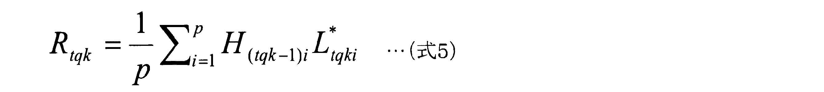
なお、各サブスペクトラムの信号成分は、DFT処理により周波数軸上で離散化されている。ここで、図18(c)に示すように、サブスペクトラムSStqkの低周波数側の遷移域において離散化された信号成分を低周波数側からLtqk1,Ltqk2,…,Ltqkp高周波数側の遷移域において離散化された信号成分を低周波数側からHtqk1,Htqk2,…,Htqkpとする。pは、DFT処理により周波数領域に生成される離散化された信号点の内、遷移域の帯域に含まれる信号成分の数である。例えば、DFT処理の周波数分解能がr、遷移域の帯域幅がBtのとき、p=[Bt/r]となる。ただし、記号[x]はxを超えない最大の整数を示す。 Note that the signal components of each sub-spectrum are discretized on the frequency axis by DFT processing. Here, as shown in FIG. 18C , the signal components discretized in the transition region on the low frequency side of the sub-spectrum SS tqk from the low frequency side to the L tqk1 , L tqk2 ,..., L tqkp high frequency side. Let the signal components discretized in the transition region be H tqk1 , H tqk2 ,..., H tqkp from the low frequency side. p is the number of signal components included in the transition band among the discrete signal points generated in the frequency domain by DFT processing. For example, when the frequency resolution of the DFT processing is r and the bandwidth of the transition band is B t , p = [B t / r]. However, the symbol [x] indicates a maximum integer not exceeding x.
位相差Rtqkは、式(5)に示すように、隣接するサブスペクトラムSStk−1の高周波数側の信号成分とSStkの低周波数側の信号成分との複素共役を乗算し、周波数軸方向に平滑化して得られる。 The phase difference R tqk is multiplied by the complex conjugate of the signal component on the high frequency side of the adjacent sub-spectrum SS tk−1 and the signal component on the low frequency side of SS tk as shown in the equation (5), and the frequency axis Obtained by smoothing in the direction.
図18(c)は、p=3のときの一例を示す。このときRtqkは式(6)で表される。 FIG. 18C shows an example when p = 3. At this time, R tqk is expressed by Equation (6).
このようにして、受信装置260は、隣接するサブスペクトラム間の位相差をDFT区間ごとに逐次推定し、送信装置150側の位相シフトで生じた位相オフセットを補償する。
In this way, receiving
従来技術では、受信装置260において、隣接するサブスペクトラム間の位相差から送信装置150の位相器105−q−1〜105−q−NDで位相シフトした位相系列を推定している。ところが、低S/N環境下や、サブスペクトラムの遷移域に存在する離散化された信号成分の数pが十分ではない場合、位相差Rtqkの推定誤差が増大する。その結果、受信装置260において、受信信号のビット誤り率(BER(Bit Error Rate))特性が劣化するという課題が生じる。また、従来技術では、平滑化する区間において、フェージングにより時間的もしくは周波数的に電力が変動する区間が含まれる場合、位相差Rtqkの推定誤差が増大する。その結果、受信信号のビット誤り率特性が劣化するという課題が生じる。
In the prior art, the receiving
本発明は、受信側における位相の推定精度を向上し、低S/N環境下や、サブスペクトラムの遷移域に存在する離散化された信号成分の数pの不足などにより劣化する受信信号のBER特性を向上できる通信システムおよび通信方法を提供することを目的とする。 The present invention improves the phase estimation accuracy on the receiving side, and deteriorates the BER of a received signal that deteriorates in a low S / N environment or due to a lack of the number p of discrete signal components existing in the transition region of the subspectrum. An object is to provide a communication system and a communication method capable of improving characteristics.
本発明に係る通信システムは、送信データを変調する変調部と、変調部が出力する変調信号を周波数領域でN(Nは3以上の整数)個のサブスペクトラムに分割し、P個(Pは2以上の整数)に複製してP個の送信信号候補を生成する分割部と、P個に複製された送信信号候補のそれぞれに対して、N個のサブスペクトラムを周波数軸上で分散配置する第1周波数遷移部と、第1周波数遷移部が分散配置前または分散配置後のN個のサブスペクトラムに対して、周波数帯域が隣接するM(2≦M≦N−1の整数)個のサブスペクトラム間の位相差が等しくなるように位相シフトを行う処理および複数の時間区間で同じ位相シフトを行う処理の少なくとも一方の処理を行う第1位相部と、分散配置および位相シフトされたN個のサブスペクトラムを加算した送信信号の信号電力の時間的な変動量が最小となる送信信号候補の信号を選択して送信する選択部とを有する送信装置と、受信信号から分散配置されたサブスペクトラムを抽出する抽出部と、分散配置されたサブスペクトラムを分散配置前の周波数帯域に戻す第2周波数遷移部と、抽出部が抽出した分散配置後または第2周波数遷移部が復元した分散配置前のサブスペクトラムに対して、周波数帯域が隣接するM個のサブスペクトラム間の重畳領域における複数の推定位相差および複数の時間区間における複数の推定位相差の少なくとも一方の推定位相差に所定の荷重を掛けて平滑化して位相補正値を算出する位相平滑化部と、位相平滑化部が算出した位相補正値により、受信信号から抽出した分散配置後のサブスペクトラムまたは分散配置前に戻したサブスペクトラムの位相を補正する第2位相部と、第2位相部が補正したN個のサブスペクトラムを加算後に時間領域の信号に変換して受信データを復調する復調部とを有する受信装置とを備えることを特徴とする。 The communication system according to the present invention divides a modulation unit that modulates transmission data and a modulation signal output from the modulation unit into N (N is an integer of 3 or more) sub-spectra in the frequency domain, and P (P is N sub-spectrums are distributed and arranged on the frequency axis for each of the division unit that generates P transmission signal candidates by duplicating to an integer of 2 or more, and the P transmission signal candidates that are duplicated The first frequency transition unit and M (an integer of 2 ≦ M ≦ N−1) subbands whose frequency bands are adjacent to N subspectrums before or after the first frequency transition unit is distributed. A first phase unit that performs at least one of a process of performing phase shift so that the phase difference between the spectrums is equal and a process of performing the same phase shift in a plurality of time intervals; and N pieces of distributed arrangement and phase shifted Subspectra And a selection unit that selects and transmits a signal of a transmission signal candidate that minimizes the amount of temporal variation in the signal power of the transmission signal, and extracts sub-spectrums that are distributed from the received signal An extraction unit, a second frequency transition unit that returns the sub-spectrum that has been distributed to the frequency band before the distributed allocation, and a sub-spectrum after the distributed allocation extracted by the extraction unit or before the distributed allocation restored by the second frequency transition unit On the other hand, smoothing is performed by applying a predetermined load to at least one of a plurality of estimated phase differences in a superimposed region between M sub-spectrums having adjacent frequency bands and a plurality of estimated phase differences in a plurality of time intervals. The phase smoothing unit for calculating the phase correction value and the phase correction value calculated by the phase smoothing unit to the sub-spectrum after dispersion arrangement extracted from the received signal. Is a second phase unit for correcting the phase of the sub-spectrum returned before the dispersion arrangement, and a demodulating unit for demodulating the received data by adding the N sub-spectrums corrected by the second phase unit to a time domain signal after addition And a receiving device.
本発明に係る通信方法は、送信装置側において、変調信号を周波数領域でN(Nは3以上の整数)個のサブスペクトラムに分割し、P個(Pは2以上の整数)に複製してP個の送信信号候補を生成する処理と、P個に複製された送信信号候補のそれぞれに対して、N個のサブスペクトラムを周波数軸上で分散配置する処理と、分散配置前または分散配置後のN個のサブスペクトラムに対して、周波数帯域が隣接するM(2≦M≦N−1の整数)個のサブスペクトラム間の位相差が等しくなるように位相シフトを行う処理および複数の時間区間で同じ位相シフトを行う処理の少なくとも一方の処理と、分散配置および位相シフトされたN個のサブスペクトラムを加算した送信信号の信号電力の時間的な変動量が最小となる送信信号候補の信号を選択して送信する処理とを行い、受信装置側において、受信信号から分散配置されたサブスペクトラムを抽出する処理と、分散配置されたサブスペクトラムを分散配置前の周波数帯域に戻す処理と、分散配置後または復元した分散配置前のサブスペクトラムに対して、周波数帯域が隣接するM個のサブスペクトラム間の重畳領域における複数の推定位相差および複数の時間区間における複数の推定位相差の少なくとも一方の推定位相差に所定の荷重を掛けて平滑化して位相補正値を算出する処理と、位相補正値により、受信信号から抽出した分散配置後のサブスペクトラムまたは分散配置前に戻したサブスペクトラムの位相を補正する処理と、位相補正されたN個のサブスペクトラムを加算後に時間領域の信号に変換して受信データを復調する処理とを行うことを特徴とする。 In the communication method according to the present invention, the modulation signal is divided into N (N is an integer of 3 or more) sub-spectrums in the frequency domain, and is copied into P (P is an integer of 2 or more) on the transmission device side. Processing for generating P transmission signal candidates, processing for distributing N sub-spectrums on the frequency axis for each of the P transmission signal candidates, and before or after distributed allocation Process for performing phase shift so that the phase difference between M (an integer of 2 ≦ M ≦ N−1) frequency bands adjacent to each other in N sub-spectrums is equal, and a plurality of time intervals The signal of the transmission signal candidate that minimizes the amount of temporal variation in the signal power of the transmission signal obtained by adding at least one of the processes for performing the same phase shift in the above and the N sub-spectrums that are distributed and phase-shifted is added. Processing to select and transmit, on the receiving device side, processing to extract the sub-spectrum distributed from the received signal, processing to return the sub-spectrum that has been distributed to the frequency band before the distribution, and distributed arrangement Estimation of at least one of a plurality of estimated phase differences in a superimposed region between M sub-spectrums whose frequency bands are adjacent to each other and a plurality of estimated phase differences in a plurality of time intervals with respect to a sub-spectrum before or after distributed reconstruction Processing to calculate the phase correction value by smoothing the phase difference by applying a predetermined load, and correcting the phase of the sub-spectrum after dispersion placement extracted from the received signal or the sub-spectrum returned before dispersion placement by the phase correction value Processing, and adding the N sub-spectrums whose phases have been corrected, and then converting them into time domain signals to demodulate the received data And performing a process.
本発明に係る通信システムおよび通信方法は、送信側において、複数のDFT区間で共通の位相シフト量となるように位相シフトを行い、複数のDFT区間内において送信信号の電力の時間的な変動が最も小さい信号を送信する。そして、受信側においては、送信側と同様のDFT区間もしくはそれ以下の長さのDFT区間で時間方向の位相推定値の荷重付き平滑化処理を行うこと、周波数方向においても共通の遷移域内にて受信電力強度に応じた荷重付き平滑化処理を行うこと、の少なくとも1つの処理を行う。これにより、受信側における位相の推定精度を向上し、低S/N環境や、サブスペクトラムの遷移域に存在する離散化された信号成分の数pの不足で劣化する受信信号のBER特性を向上することができる。 In the communication system and the communication method according to the present invention, on the transmission side, phase shift is performed so that a common phase shift amount is obtained in a plurality of DFT sections, and the temporal variation of the power of the transmission signal occurs in the plurality of DFT sections. Send the smallest signal. On the receiving side, the weighted smoothing process of the phase estimation value in the time direction is performed in the same DFT interval as that on the transmitting side or a DFT interval having a length shorter than that, and within the common transition region also in the frequency direction. At least one process of performing a weighted smoothing process according to the received power intensity is performed. This improves the phase estimation accuracy on the receiving side, and improves the BER characteristics of received signals that deteriorate due to a low S / N environment or the lack of the number p of discrete signal components present in the sub-spectrum transition region. can do.
或いは、送信側において、位相シフト後にサブスペクトラム間の位相差が複数のサブスペクトラムで同じ値となるよう設定する。これにより、位相シフト量は、時間方向ではなく周波数方向においても同じ値に設定される。送信側のそして、受信側において、複数のサブスペクトラムの位相差の荷重付き平滑化処理を行う。これにより、受信側における位相の推定精度を向上し、低S/N環境や、サブスペクトラムの遷移域に存在する離散化された信号成分の数pの不足で劣化する受信信号のBER特性を向上することができる。 Alternatively, the transmission side is set so that the phase difference between the sub-spectrums becomes the same value in the plurality of sub-spectrums after the phase shift. Thereby, the phase shift amount is set to the same value not in the time direction but also in the frequency direction. On the transmission side and on the reception side, a weighted smoothing process is performed for the phase differences of a plurality of subspectrums. This improves the phase estimation accuracy on the receiving side, and improves the BER characteristics of received signals that deteriorate due to a low S / N environment or the lack of the number p of discrete signal components present in the sub-spectrum transition region. can do.
また、フェージングにより、平滑化する区間において、時間的もしくは周波数的に電力が変動する区間が含まれる場合、該当区間の荷重を小さくするか、該当区間を使用しないようにする。これにより、フェージングの影響が軽減され、位相差Rtqkの推定誤差を小さくすることができる。その結果、受信信号のBER特性が向上することができるという効果が得られる。 In addition, when the section to be smoothed due to fading includes a section in which power fluctuates in time or frequency, the load of the corresponding section is reduced or the corresponding section is not used. Thereby, the influence of fading is reduced and the estimation error of the phase difference R tqk can be reduced. As a result, an effect that the BER characteristic of the received signal can be improved is obtained.
なお、位相推定精度の向上により、必要となるサブスペクトラムの遷移域を削減できるので、スペクトラムの占有帯域を削減でき、周波数利用効率が向上するという効果も得られる。 In addition, since the required sub-spectrum transition area can be reduced by improving the phase estimation accuracy, it is possible to reduce the occupied band of the spectrum and improve the frequency utilization efficiency.
以下、図面を参照して本発明に係る通信システムおよび通信方法の実施形態について説明する。
(第1実施形態)
[送信装置50]
図1は、本実施形態に係る通信システム70における送信装置50の一例を示す。なお、本実施形態では、通信システム70は、送信装置50と受信装置60とを有する。
Embodiments of a communication system and a communication method according to the present invention will be described below with reference to the drawings.
(First embodiment)
[Transmitter 50]
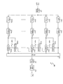
FIG. 1 shows an example of a
図1において、送信装置50は、変調回路1、波形整形フィルタ2、DFT回路3、分割フィルタ4−1〜4−ND、位相器5−1−1〜5−C−ND、周波数シフタ6−1−1〜6−C−ND、加算器7−1〜7−C、IDFT回路8−1〜8−C、PAPR算出回路9−1〜9−C、バッファ10−1−1〜バッファ10−C−1、バッファ10−1−2〜バッファ10−C−2および最小PAPR信号選択器11を有する。ここで、NDおよびCは正の整数である。
In FIG. 1, a
変調回路1は、送信データをQPSKなどの変調方式で変調する。
The
波形整形フィルタ2は、変調回路1が出力する変調信号の帯域を制限するためのフィルタである。
The
DFT回路3は、波形整形フィルタ2から出力される変調信号を所定のDFT区間ごとに逐次周波数領域(スペクトラム)の信号に変換する。ここで、処理時刻が早いものから順に“1番目のDFT区間”,“2番目のDFT区間”,…,“t番目のDFT区間”,…,“t+u番目のDFT区間”,…と称する。なお、t,uは正の整数である。
The
分割フィルタ4−k(1≦k≦ND)は、DFT回路3がDFT区間毎に周波数領域に変換した変調信号の帯域をND個に分割する。分割フィルタ4−1〜4−NDは、予め設定されたフィルタ係数を変調信号に乗算することで、ND個のサブ変調信号(サブスペクトラム)を生成する。そして、分割フィルタ4−kのそれぞれの出力信号はC個に分岐される。ここで、kは正の整数である。サブスペクトラムを処理時刻が早いものから順に“1番目のDFT区間のサブスペクトラム”,“2番目のDFT区間のサブスペクトラム”,…,“t番目のDFT区間のサブスペクトラム”,…,“t+u番目のDFT区間のサブスペクトラム”,…と称する。なお、分割フィルタ4−kは、従来技術で説明した図16(a)および図16(b)と同様に動作する。
The division filter 4-k (1 ≦ k ≦ N D ) divides the modulated signal band converted by the
位相器5−q−k(1≦q≦C,1≦k≦ND)は、C個に分岐された分割フィルタ4−k(1≦k≦ND)の出力をそれぞれ入力する。ここで、qは正の整数である。例えば、C個の内の1番目のND個のサブスペクトラムは位相器5−1−k、2番目のND個のサブスペクトラムは位相器5−2−k、…、C番目のND個のサブスペクトラムは位相器5−C−kにそれぞれ入力される。ここで、位相系列制御装置51は、位相器5−C−kに位相情報を出力する。位相系列制御装置51から出力される位相情報は、例えば、ランダムに生成した位相値や、円を等分割(2πを等分割)することで生成される位相の組み合わせなどが使用される。なお、位相情報は、受信装置60と共有される。そして、位相器5−C−kは、位相系列制御装置51から入力する位相情報に基づいて各サブスペクトラムに位相シフトを付加する。
The phase shifter 5-q-k (1 ≦ q ≦ C, 1 ≦ k ≦ N D ) inputs the outputs of the C divided filters 4-k (1 ≦ k ≦ N D ), respectively. Here, q is a positive integer. For example, the first N D sub spectrum phaser 5-1-k, 2-th N D sub spectrum phaser 5-2-k of the number C, ..., C-th N D The sub-spectrums are respectively input to the phase shifters 5-C-k. Here, the phase
例えば、本実施形態では、位相器5−q−kは、式(7)で示す位相系列Θ2,Θ3,…,Θq,…,ΘCを用いて、位相器5−q−kに入力された各サブスペクトラムの位相をシフトする。 For example, in this embodiment, the phase shifter 5-q-k, the phase sequence theta 2 represented by the formula (7), Θ 3, ... , Θ q, ..., using a theta C phaser 5-q-k The phase of each subspectrum input to is shifted.
ここで、位相器5−q−kに入力されるt番目のDFT区間のサブスペクトラムをSStkとする。そして、位相器5−q−kは、式(8)で示す位相系列Θqの位相により、式(9)で示すt番目のDFT区間のサブスペクトラムSStkの位相シフトを行う。 Here, the sub-spectrum of the t-th DFT interval input to the phase shifter 5-qk is SS tk . Then, the phase shifter 5-q-k shifts the phase of the sub-spectrum SS tk in the t-th DFT section shown in Expression (9) based on the phase of the phase sequence Θ q shown in Expression (8).
![]()
![]()
位相乗算後の位相器5−q−kの出力信号Sθ tqは式(10)となる。 The output signal S θ tq of the phase shifter 5-qk after the phase multiplication is expressed by Equation (10).
周波数シフタ6−q−k(1≦q≦C,1≦k≦ND)は、各サブスペクトラムを周波数軸上の所望の帯域に分散配置する。ここで、周波数シフタ6−2−kの各サブスペクトラム、周波数シフタ6−3−kの各サブスペクトラム、…、周波数シフタ6−C−kの各サブスペクトラムは、周波数シフタ6−1−kの各サブスペクトラムと同様のシフト量だけ周波数シフトさせて分散配置する。 The frequency shifter 6-qk (1 ≦ q ≦ C, 1 ≦ k ≦ N D ) disperses and arranges each sub-spectrum in a desired band on the frequency axis. Here, each sub-spectrum of the frequency shifter 6-2-k, each sub-spectrum of the frequency shifter 6-3-k,..., Each sub-spectrum of the frequency shifter 6-C-k is the frequency shifter 6-1-k. The frequency is shifted by the same shift amount as that of each sub-spectrum, and is distributed.
加算器7−q(1≦q≦C)は、周波数シフタ6−q−kの出力信号を各組毎(同じq毎)にND個のサブスペクトラムを加算する。 The adder 7-q (1 ≦ q ≦ C) adds the N D sub spectrum output signal of the frequency shifter 6-q-k for each set (each equivalent q).
IDFT回路8−q(1≦q≦C)は、加算器7−qの出力信号を周波数領域の信号から時間領域の信号に変換する。例えば、IDFT8−1は、加算器7−1の出力信号を周波数領域の信号から時間領域の信号に変換する。 The IDFT circuit 8-q (1 ≦ q ≦ C) converts the output signal of the adder 7-q from a frequency domain signal to a time domain signal. For example, the IDFT 8-1 converts the output signal of the adder 7-1 from a frequency domain signal to a time domain signal.
PAPR算出回路9−q(1≦q≦C)は、IDFT8−qで時間領域の信号に変換された信号についてPAPRを算出する。 The PAPR calculation circuit 9-q (1 ≦ q ≦ C) calculates the PAPR for the signal converted into the time domain signal by the IDFT8-q.
以下、PAPR算出回路9−qと、PAPR算出回路9−qが算出したPAPRを格納するバッファ10−q−1と、最小PAPR信号選択器11との動作について説明する。例えば、PAPR算出回路9−qは、IDFT8−qが出力する1番目のDFT区間の信号に着目し、電力の時間的な変動量を算出する。ここで、電力の時間的な変動を表す数値として、本実施形態では、信号の一定時間区間における最大の電力と平均の電力の比(PAPR)を使用する。算出されたPAPRは、バッファ10−q−1に格納される。以降、PAPR算出回路9−qは、u番目のDFT区間までPAPRの算出を行う。ここで、PAPR算出回路9−qは、算出したu通りのPAPRから特定の規範に従って代表値を算出する。本実施形態では、特定の規範として、u通りのPAPRの和を取った値を代表値とする。このPAPR算出処理および代表値の算出は、分岐したC通りの全ての信号について行われる。そして、最小PAPR信号選択器11は、C通りの代表値の中でPAPRが最も小さい信号を選択して送信する。ここで、PAPRは、入力される信号に対して2乗した値の最大値と平均値とを求め、最大値/平均値(最大値を平均値で割った値)を計算することにより算出できる。
Hereinafter, operations of the PAPR calculation circuit 9-q, the buffer 10-q-1 that stores the PAPR calculated by the PAPR calculation circuit 9-q, and the minimum
このようにして、送信装置50は、送信データを変調して複数のサブスペクトラムに分割し、位相シフトおよび周波数シフトを行って加算した信号のPAPRを算出し、PAPRが最小となる位相系列θqの信号を受信装置60に送信する。
[受信装置60]
図2は、本実施形態に係る通信システム70の受信装置60の一例を示す。図2において、受信装置60は、DFT回路21、抽出フィルタ22−1〜22−ND、周波数シフタ23−1〜23−ND、位相差推定器24−2〜24−ND、荷重付平滑化回路25−2〜25−ND、荷重算出器26−2〜26−ND、バッファ27−2〜27−ND、荷重算出器28−2〜28−ND、荷重付平滑化回路29−2〜29−ND、バッファ30−2〜30−ND、位相器31−2〜31−ND、加算器32、IDFT回路33、復調回路34および位相平滑化数制御装置61を有する。
In this way, the
[Receiver 60]
FIG. 2 shows an example of the receiving
ここで、受信装置60は、送信装置50で位相シフトする前のスペクトラムを復元後に復調する必要がある。そこで、送信装置50は、特定のサブスペクトラムの位相シフト量を位相の基準として位相シフトせずに固定し、この固定するサブスペクトラムの情報を送信装置50と受信装置60との間で共有する。本実施形態では、最も周波数が低いサブスペクトラム(SSt1)の位相シフト量を0とする。
Here, the receiving
以下、図2の受信装置60について説明する。
Hereinafter, the receiving
DFT回路21は、送信装置50からの受信信号を周波数領域の信号に変換する。
The
抽出フィルタ22−k(1≦k≦ND)は、ND個に分岐されたDFT回路21の出力信号をそれぞれ入力し、ND個のサブスペクトラムを抽出する。
Extraction filter 22-k (1 ≦ k ≦ N D) is the output signal of the
周波数シフタ23−k(1≦k≦ND)は、抽出フィルタ22−1〜22−NDが出力する各サブスペクトラムを送信装置50の周波数シフタ6−q−1〜6−q−NDが周波数シフトする前の帯域に戻すようにシフトする。
Frequency shifter 23-k (1 ≦ k ≦ N D) , the extraction filter 22-1 to 22-N D frequency shifter of the
位相差推定器24−k(2≦k≦ND)は、周波数シフタ23−1〜23−NDのうち隣接するサブスペクトラムの信号の位相差を推定する。図2において、例えば、位相差推定器24−2は、周波数シフタ23−1と周波数シフタ23−2とのそれぞれの出力信号を入力し、送信装置50の位相器5−q−2で位相シフトした位相差を推定する。なお、位相差の推定方法は後述する。
Phase difference estimator 24-k (2 ≦ k ≦ N D) estimates the phase difference of the sub-spectrum of a signal that adjacent ones of the frequency shifters 23-1 to 23-N D. In FIG. 2, for example, the phase difference estimator 24-2 inputs the output signals of the frequency shifter 23-1 and the frequency shifter 23-2, and the phase shifter 5-q-2 of the
荷重付平滑化回路25−k(2≦k≦ND)は、位相差推定器24−kの出力信号を入力し、荷重付きの平滑化を行う。 Load with the smoothing circuit 25-k (2 ≦ k ≦ N D) receives the output signal of the phase difference estimator 24-k, smoothing with load.
荷重算出器26−k(2≦k≦ND)は、位相差推定器24−kの出力信号に基づいて、荷重値を算出する。 The load calculator 26-k (2 ≦ k ≦ N D ) calculates a load value based on the output signal of the phase difference estimator 24-k.
バッファ27−k(2≦k≦ND)は、荷重付平滑化回路25−kが出力する信号を格納する。 The buffer 27-k (2 ≦ k ≦ N D ) stores a signal output from the weighted smoothing circuit 25-k.
荷重算出器28−k(2≦k≦ND)は、バッファ27−kに格納されたu通りのDFT区間の信号を基に荷重値を算出する。 The load calculator 28-k (2 ≦ k ≦ N D ) calculates a load value based on u-way DFT section signals stored in the buffer 27-k.
荷重付平滑化回路29−k(2≦k≦ND)は、荷重算出器28−kが算出した荷重値を用いて、バッファ27−kに格納されているu通りのDFT区間の信号を荷重付きで平滑化する。 The load smoothing circuit 29-k (2 ≦ k ≦ N D ) uses the load value calculated by the load calculator 28-k to output u-way DFT section signals stored in the buffer 27-k. Smooth with load.
バッファ30−k(2≦k≦ND)は、周波数シフタ23−k(2≦k≦ND)が出力する信号を格納する。 The buffer 30-k (2 ≦ k ≦ N D ) stores a signal output from the frequency shifter 23-k (2 ≦ k ≦ N D ).
位相器31−k(2≦k≦ND)は、荷重付平滑化回路29−kが出力する位相シフト量に基づいて、バッファ30−kに格納されたSStqkからSS(t+u)qkまでのサブスペクトラムの位相を補償する。 The phase shifter 31-k (2 ≦ k ≦ N D ) is configured from SS tqk stored in the buffer 30-k to SS (t + u) qk based on the phase shift amount output from the weighted smoothing circuit 29-k. Compensate the phase of the subspectrum.
加算器32は、位相器31−kが出力する位相補償されたND個のサブスペクトラムを加算して分割前のスペクトラムを復元する。
IDFT回路33は、加算器32が出力するスペクトラムを入力して時間領域の信号に変換する。
The
復調回路34は、IDFT回路33が出力する変調信号を復調して受信データを出力する。例えば、送信装置50の変調回路1がQPSKで変調した場合は、同じQPSKで受信データを復調する。
The
位相平滑化数制御装置61は、荷重付平滑化回路29−kが位相を平滑化するときの平滑化数を制御する。なお、平滑化数については後述する。
The phase smoothing
このようにして、受信装置60は、送信装置50から受信する信号を復調することができる。特に、本実施形態に係る受信装置60は、分散配置前の帯域に戻したサブスペクトラムに対して、隣接するサブスペクトラム間の重畳領域の位相差から位相シフト量を推定して荷重付きで平滑化する(周波数領域での平滑化)。さらに、u+1個のDFT区間において、周波数領域で平滑化した位相シフト量を荷重付きで平滑化する(時間領域での平滑化)。これにより、本実施形態では、受信側における位相の推定精度を向上し、低S/N環境下や、サブスペクトラムの遷移域に存在する離散化された信号成分の数pの不足などにより劣化する受信信号のBER特性を向上することができる。
In this way, the
次に、受信装置60の位相差推定器24−kの動作について詳しく説明する。位相差推定器24−kは、周波数領域で隣接するサブスペクトラム(SStqk−1とSStqk)の遷移域における位相差Rtqkを計算する。ここで、送信装置50において、各サブスペクトラムの遷移域同士は重畳しているため、隣接するサブスペクトラムの遷移域は同一の信号成分を含んでいる。受信装置60では、送信装置50で重畳している遷移域(重畳領域)の信号成分から位相差Rtqkを推定する。
Next, the operation of the phase difference estimator 24-k of the receiving
なお、周波数が一番低いサブスペクトラムSSt1kは、送信装置50で位相シフトが行われていないため、まず、位相差推定器24−2は、周波数シフタ23−1および周波数シフタ23−2から出力されるSSt1kおよびSSt2kを用いて、SSt2kの位相シフト量Rt2kを推定する。そして、推定値^θtq2=atan(Rt2k)は、荷重付平滑化回路25−2で平滑化され、その出力はu個分のDFT区間でバッファ27−2に蓄積される。その後、荷重付平滑化回路29−2は、u個のDFT区間で受信電力レベルに応じた荷重付きの平滑化処理を行う。そして、位相器31−2は、荷重付きの平滑化処理が行われた位相シフト量を入力し、周波数シフタ23−2の出力信号にexp(−j(^θtq2))を乗算して位相を補償する。
Note that the phase difference estimator 24-2 is first output from the frequency shifter 23-1 and the frequency shifter 23-2 because the phase shift of the sub-spectrum SS t1k having the lowest frequency is not performed by the
なお、荷重付平滑化回路29−2は、t番目からt+u番目のDFT区間における位相推定値Rt2kからR(t+u)2kまでのu個の位相推定値の平滑化、もしくはt番目からt+u番目以下のDFT区間での平滑化を行い、平滑化した結果を出力する。このとき、t番目からt+u番目のDFT区間において、DFT区間ごとに受信電力強度が異なる場合、受信電力強度が高い信号ほど信号対雑音電力比(S(signal)/N(Noise))が良い確率が高いとみなし、荷重算出器28−2で受信電力強度に応じた荷重を求め、荷重付平滑化回路29−2で荷重付の平滑化を行う。 The weighted smoothing circuit 29-2 smoothes the u phase estimation values from the phase estimation values R t2k to R (t + u) 2k in the t-th to t + u-th DFT interval, or the t-th to t + u-th. Smoothing is performed in the following DFT interval, and the smoothed result is output. At this time, in the t-th to t + u-th DFT interval, when the received power intensity is different for each DFT interval, the higher the received power intensity, the better the signal-to-noise power ratio (S (signal) / N (Noise)) The load calculator 28-2 obtains a load corresponding to the received power intensity, and the load smoothing circuit 29-2 performs load smoothing.
ここで、受信電力強度が一定の場合、荷重付平滑化回路29−2は、式(11)に示す計算を行う。 Here, when the received power intensity is constant, the weighted smoothing circuit 29-2 performs the calculation shown in Expression (11).
また、受信電力強度が一定でない場合、荷重付平滑化回路29−2は、受信電力に応じた荷重をwtq2、wtq2、wtq2,w(t+1)q2,…,w(t+u)q2として、式(12)に示す計算を行う。 When the received power intensity is not constant, the weighted smoothing circuit 29-2 sets the load corresponding to the received power as w tq2 , w tq2 , w tq2 , w (t + 1) q2 ,..., W (t + u) q2. The calculation shown in the equation (12) is performed.
ここで、wは例えば電力強度に比例した値でもよいし、電力強度の2乗に比例した値でもよい。 Here, w may be a value proportional to the power intensity, for example, or may be a value proportional to the square of the power intensity.
同様に、位相差推定器24−3は、位相器31−2で位相補償された信号SStq2と、周波数シフタ23−3の出力信号SStq3とを入力し、位相シフト量Rtq3を推定する。そして、荷重付平滑化回路25−3で平滑化された位相シフト量がt番目からt+u番目までのDFT区間でバッファ27−3に格納される。荷重付平滑化回路29−3は、t番目からt+u番目までのDFT区間の位相シフト量を平滑化し、位相器21−3に平滑化後の位相シフト量(^θtq3)を出力する。位相器31−3は、荷重付平滑化回路29−3の出力を用いて周波数シフタ23−3から出力されるSStq3にexp(−j(^θtq3))を乗算し、位相を補償する。 Similarly, the phase difference estimator 24-3 receives the signal SS tq2 phase-compensated by the phase shifter 31-2 and the output signal SS tq3 of the frequency shifter 23-3, and estimates the phase shift amount R tq3 . . Then, the phase shift amount smoothed by the weighted smoothing circuit 25-3 is stored in the buffer 27-3 in the DFT interval from the tth to the t + uth. The weighted smoothing circuit 29-3 smoothes the phase shift amount of the DFT section from the t-th to the t + u-th, and outputs the smoothed phase shift amount (^ θ tq3 ) to the phase shifter 21-3. The phase shifter 31-3 uses the output of the weighted smoothing circuit 29-3 to multiply SS tq3 output from the frequency shifter 23-3 by exp (−j (^ θ tq3 )) to compensate the phase. .
以降、位相差推定器24−k(4≦k≦ND)は、位相器31−(k−1)から出力されたSStq(k−1)と周波数シフタ23−kから出力されたSStqkとから位相シフト量Rtqkを推定する。そして、荷重付平滑化回路25−kで平滑化された位相シフト量は、t番目からt+u番目までのDFT区間でバッファ27−kに格納される。荷重付平滑化回路29−kは、t番目からt+u番目までのDFT区間の位相シフト量を平滑化し、位相器21−kに平滑化後の位相シフト量(^θtqk)を出力する。そして、位相器31−kは、荷重付平滑化回路29−kの出力を用いて周波数シフタ23−kから出力され、バッファ30−kに蓄積されたSStqkにexp(−j(^θtqk))を乗算し、位相を補償する。 Thereafter, the phase difference estimator 24-k (4 ≦ k ≦ N D) is a phase shifter 31- (k-1) outputted from the SS tq (k-1) and SS output from the frequency shifter 23-k The phase shift amount R tqk is estimated from tqk . Then, the phase shift amount smoothed by the weighted smoothing circuit 25-k is stored in the buffer 27-k in the D-th section from the t-th to the t + u-th. The weighted smoothing circuit 29-k smoothes the phase shift amount of the DFT section from the t-th to the t + u-th, and outputs the smoothed phase shift amount (^ θ tqk ) to the phase shifter 21-k. Then, the phase shifter 31-k outputs exp (−j (^ θ tqk ) to SS tqk output from the frequency shifter 23-k using the output of the weighted smoothing circuit 29-k and accumulated in the buffer 30-k. )) To compensate for the phase.
ここで、各サブスペクトラムの信号成分は、DFT処理により周波数軸上で離散化されている。また、従来技術の図18(c)で説明したように、サブスペクトラムSStqkの低周波数側の遷移域において離散化された信号成分を低周波数側からLtqk1,Ltqk2,…,Ltqkpとし、高周波数側の遷移域において離散化された信号成分を低周波数側からHtqk1,Htqk2,…,Htqkpとする。ただし、pは、DFT処理により生成される離散化された信号点の内、遷移域の帯域に含まれる信号成分の数である。例えば、DFTの周波数分解能がr、遷移域の帯域幅がBtのとき、p=[Bt/r]となる。ここで、記号[x]はxを超えない最大の整数を示す。 Here, the signal components of each sub-spectrum are discretized on the frequency axis by DFT processing. Further, as described in FIG. 18C of the prior art, the signal components discretized in the transition region on the low frequency side of the sub-spectrum SS tqk are set to L tqk1 , L tqk2 ,..., L tqkp from the low frequency side. , H tqk1 , H tqk2 ,..., H tqkp are signal components discretized in the transition region on the high frequency side from the low frequency side. However, p is the number of signal components included in the band of the transition region among the discretized signal points generated by the DFT processing. For example, when the frequency resolution of the DFT is r and the bandwidth of the transition region is B t , p = [B t / r]. Here, the symbol [x] indicates a maximum integer not exceeding x.
位相差Rtqkは、隣接するサブスペクトラムSStqk−1およびSStqkの高周波数側の信号成分と低周波数側の信号成分の複素共役を乗算し、周波数軸方向に平滑化して得られる。ここで、同じ遷移域内に存在する離散化された信号成分(Ltqk1,Ltqk2,…,Ltqkpなど)の電力強度に違いがある場合、強度が高い信号ほど信号対雑音電力比(S/N)が良い確率が高いとみなし、受信電力強度に応じた荷重を設定して、荷重付の平滑化を行う。 The phase difference R tqk is obtained by multiplying the complex component of the signal component on the high frequency side and the signal component on the low frequency side of the adjacent sub-spectrums SS tqk−1 and SS tqk and smoothing in the frequency axis direction. Here, when there is a difference in power intensity of discretized signal components (L tqk1 , L tqk2 ,..., L tqkp, etc.) existing in the same transition region, the signal-to-noise power ratio (S / N) is considered to have a high probability, and a load corresponding to the received power intensity is set to perform smoothing with a load.
式(13)は、荷重付き平均を用いない場合の平滑化処理を示す。 Equation (13) shows the smoothing process when the weighted average is not used.
p=3の場合、Rtqkは式(14)で表される。 In the case of p = 3, R tqk is expressed by Expression (14).
また、荷重の値をvtqkiとすると、荷重付き平均を用いる場合の平滑化処理は、式(15)で表される。 Further, when the load value is v tqki , the smoothing process in the case of using the weighted average is expressed by Expression (15).
ここで、vtqkiは、例えば電力強度に比例した値でもよいし、電力強度の2乗に比例した値でもよい。 Here, v tqki may be a value proportional to the power intensity, for example, or may be a value proportional to the square of the power intensity.
このようにして、受信装置60は、隣接するサブスペクトラム間の位相差をDFT区間ごとに逐次推定し、送信装置50側での位相シフト処理により生じた位相オフセットを補償することができる。
In this way, the receiving
次に、本実施形態に係る送信装置50において、隣接する複数のサブスペクトラム間の位相差が等しくなるように位相シフトを行う例について説明する。
Next, an example will be described in which the phase shift is performed so that the phase differences between a plurality of adjacent sub-spectrums are equal in the
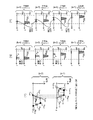
図3は、隣接する2つのサブスペクトラム間の位相差が等しくなるように位相シフトを行う一例を示す。ここで、スペクトラムの分割数ND=8、隣接するサブスペクトラム数M=2とする。隣接するサブスペクトラム間の位相差が等しくなるように位相シフトを行う処理は、複数のDFT区間(例えば8個のDFT区間)の各DFT区間において行われ、図3の例では、ある1つのDFT区間における8個のサブスペクトラムについて処理が行われる。ここで、Mは「同じ位相シフト(位相回転)が加わっているサブスペクトラム」の数を表し、Mは2≦M≦ND−1の整数である。例えば、図3において、サブスペクトラム3とサブスペクトラム4の2個のサブスペクトラム間の位相差が同じΔθ1になるように位相シフトが行われる。同様に、サブスペクトラム1とサブスペクトラム2の2個のサブスペクトラム間の位相差は0、サブスペクトラム5とサブスペクトラム6の2個のサブスペクトラム間の位相差はΔθ2、サブスペクトラム7とサブスペクトラム8の2個のサブスペクトラム間の位相差はΔθ3、となるように位相シフトが行われる。
FIG. 3 shows an example in which the phase shift is performed so that the phase difference between two adjacent sub-spectrums becomes equal. Here, it is assumed that the number of spectrum divisions N D = 8 and the number of adjacent sub-spectrums M = 2. The process of performing the phase shift so that the phase differences between adjacent sub-spectrums are equal is performed in each DFT section of a plurality of DFT sections (for example, eight DFT sections). In the example of FIG. Processing is performed on eight sub-spectrums in the section. Here, M represents the number of “sub-spectrums to which the same phase shift (phase rotation) is added”, and M is an integer of 2 ≦ M ≦ N D −1. For example, in FIG. 3, the phase shift is performed so that the phase difference between the two sub-spectrum of the
このように、本実施形態に係る送信装置50は、周波数帯域が隣接するM個のサブスペクトラム間の位相差が等しくなるように位相シフトを行っている。
As described above, the
また、送信装置50は、同一のDFT区間において、位相器5−q−kに与える位相シフト量が隣接するM個(2≦M≦ND−1)のサブスペクトラム間の位相差が等しくなるように位相シフトを行い、受信装置60は、位相平滑化数制御装置61から出力される平滑化するサブスペクトラム数Mの値に基づいて、M個のサブスペクトラムの重畳領域での位相差を単純平均もしくは荷重付きで平滑化を行う。これにより、受信側での位相推定精度を向上することができる。ここで、荷重付き平滑化処理を行うときの荷重は、例えば、受信電力強度に応じて設定することができる。この場合、受信電力強度が強くなるほど荷重を大きくし、逆に受信電力強度が弱くなるほど荷重を小さくする。
Further, in the same DFT section, the
また、送信側で使用する全ての位相シフト量の値θqkを送信装置50と受信装置60との間で予め共有しておき、位相の硬判定により受信側の位相推定値に最も近い位相シフト量の値θqkを用いて位相補償を行うことにより、受信装置60での位相推定精度を向上することもできる。
Further, all phase shift amount values θ qk used on the transmission side are shared in advance between the
また、図1に示した送信装置50の構成において、周波数シフタ6−q−kを位相器5−q−kと加算器7−qとの間ではなく、分割フィルタ4−kと位相器5−q−kとの間に配置し、周波数シフタ6−q−kでサブスペクトラムを分散配置後に、各サブスペクトラムに対して位相器5−q−kが位相シフトするようにしてもよい。
Further, in the configuration of the
また、送信装置50がPAPRを算出するDFT区間の長さを示す情報は、受信装置60側で既知である必要があるが、例えば送信装置50と受信装置60とが通信を開始する時に、送信装置50から受信装置60に当該情報を通知するようにしてもよいし、受信装置60が受信信号から推定するようにしてもよい。
Further, the information indicating the length of the DFT section for which the
また、図2に示した受信装置60の構成において、周波数シフタ23−kを抽出フィルタ22−kと位相差推定器24−kとの間ではなく、位相器31−kと加算器32−kとの間に配置してもよい。
[送信処理]
図4は、本実施形態における送信処理の一例を示す。なお、図4の送信処理は、送信装置50で行われる。
In addition, in the configuration of the receiving
[Transmission process]
FIG. 4 shows an example of transmission processing in the present embodiment. Note that the transmission processing in FIG. 4 is performed by the
ステップS101において、時間領域の信号の時間区間を示す変数t(tは正の整数)をt=1に初期化する。なお、時間区間tは、DFT回路3が処理するDFT区間の順番を示す変数tと同様に扱うことができる。例えば、時間区間tにおいてDFT処理するDFT区間の順番がtとなる。
In step S101, a variable t (t is a positive integer) indicating the time interval of the time domain signal is initialized to t = 1. The time interval t can be handled in the same manner as the variable t indicating the order of the DFT intervals processed by the
ステップS102において、時間区間tにおける送信データが変調回路1に入力される。
In step S <b> 102, transmission data in the time interval t is input to the
ステップS103において、変調回路1は、入力する時間区間tの送信データをQPSKなどの変調方式で変調する。
In step S103, the
ステップS104において、波形整形フィルタ2は、窓関数などにより、変調回路1が出力する変調信号の波形を整え、DFT回路3により周波数領域の信号に変換される。
In step S104, the
ステップS105において、ND個の分割フィルタ4−kは、DFT回路3が周波数領域に変換した変調信号のスペクトラムをND個のサブスペクトラムに分割する。
In step S105, the N D divided filter 4-k divides the spectrum of the modulated
ステップS106において、1からCまでのC個の位相系列を示す変数qをq=1に初期化する。 In step S106, a variable q indicating C phase sequences from 1 to C is initialized to q = 1.
ステップS107において、位相器5−q−kは、位相系列制御装置51から与えられる位相系列制御値(位相系列θq)を基づいて、隣接するM個のサブスペクトラム間の位相差が等しくなるように位相シフトを行う。なお、位相系列制御装置51は、受信装置60との間で位相系列θqの情報を共有している。
In step S107, the phase shifter 5-q-k makes the phase difference between the adjacent M sub-spectrums equal based on the phase sequence control value (phase sequence θ q ) given from the phase
ステップS108において、周波数シフタ6−q−kは、位相器5−q−kが出力する位相シフト後の各サブスペクトラムの周波数をシフトする。なお、シフトする周波数は予め決められている。 In step S108, the frequency shifter 6-qk shifts the frequency of each subspectrum after the phase shift output from the phase shifter 5-qk. Note that the frequency to be shifted is determined in advance.
ステップS109において、加算器7−qは、ND個の周波数シフタ6−q−kがそれぞれ出力するND個のサブスペクトラムを加算し、加算後のスペクトラムは、IDFT回路8−qにより時間領域の信号に変換される。なお、IDFT回路8−qにより変換された時間領域の信号は、PAPR算出回路9−qに入力されるとともに、位相系列θq毎、且つ、時間区間t毎の時間領域の信号がバッファ10−q−2に格納される。
In step S109, the adder 7-q adds the N D sub spectrum the N D frequency shifter 6-q-k respectively output the spectrum after the addition, the time domain by IDFT circuit 8-q Is converted into a signal. The time domain signal converted by the IDFT circuit 8-q is input to the PAPR calculation circuit 9-q, and the time domain signal for each phase sequence θ q and for each time interval t is
ステップS110において、PAPR算出回路9−qは、IDFT回路8−qが出力するDFT区間tの時間領域の信号からPAPRを算出する。 In step S110, the PAPR calculation circuit 9-q calculates the PAPR from the signal in the time domain of the DFT section t output from the IDFT circuit 8-q.
ステップS111において、位相系列θqの時間区間tにおけるPAPRをバッファ10−q−1に格納する。例えば、位相系列θ1の時間区間t=1におけるPAPRがバッファ10−1−1に格納される。位相系列θ2から位相系列θCについても同様に、時間区間t=1におけるPAPRがバッファ10−2−1からバッファ10−C−1にそれぞれ格納される。また、時間区間t=2から時間区間t=u+1についても同様に、位相系列θ1から位相系列θCに対するそれぞれのPAPRがバッファ10−1−1からバッファ10−C−1にそれぞれ格納される。このようにして、位相系列θq毎、且つ、時間区間t毎に算出された各PAPRがバッファ10−q−1に格納される。 In step S111, it stores the PAPR at the time interval t of the phase sequence theta q in the buffer 10-q-1. For example, the PAPR in the time interval t = 1 of the phase sequence θ 1 is stored in the buffer 10-1-1. Similarly the phase sequence theta 2 for phase sequence theta C, PAPR in the time interval t = 1 are stored respectively from the buffer 10-2-1 in the buffer 10-C-1. Similarly, the time interval t = 2 from the time interval t = u + 1, each of the PAPR from the phase sequence theta 1 with respect to the phase sequence theta C are respectively stored from the buffer 10-1-1 in the buffer 10-C-1 . In this way, each PAPR calculated for each phase series θ q and for each time interval t is stored in the buffer 10-q-1.
ステップS112において、1からC番目までの全ての位相系列qについてステップS107からステップS111までの一連の処理が終了したか否かを判別する。一連の処理が位相系列qのC番目まで終了した場合はステップS113の処理に進み、C番目まで終了していない場合はステップS114の処理に進む。 In step S112, it is determined whether or not a series of processing from step S107 to step S111 has been completed for all the phase sequences q from 1 to C. If the series of processes has been completed up to the Cth of the phase series q, the process proceeds to step S113, and if not, the process proceeds to step S114.
ステップS113において、1から(u+1)番目までの各時間区間(DFT区間)tについてステップS102からステップS112までの処理が終了したか否かを判別し、一連の処理が(u+1)番目まで終了した場合はステップS115の処理に進み、(u+1)番目まで終了していない場合はステップS116の処理に進む。 In step S113, it is determined whether or not the processing from step S102 to step S112 has been completed for each time interval (DFT interval) t from 1 to (u + 1) th, and a series of processing has been completed to (u + 1) th. If this is the case, the process proceeds to step S115, and if not completed to the (u + 1) th, the process proceeds to step S116.
ステップS114において、次に処理する位相系列(q+1)が設定される。 In step S114, the phase sequence (q + 1) to be processed next is set.
ステップS115において、位相系列θC、且つ、時間区間t=u+1まで終了したら、最小PAPR信号選択器11は、q=Cかつt=u+1までのPAPRをバッファ10−q−1に格納し終えたら、位相系列θq(q=1〜C)によって位相シフトされたu+1個のPAPRの中で最も大きいPAPRを位相系列θq(q=1〜C)におけるPAPRの代表値として抽出する。例えば、時間区間t=3の位相系列θ2のPAPRが最大の場合、時間区間t=3の位相系列θ2のPAPRを代表値として抽出する。同様に、位相系列θ1からθCまでの位相系列毎のu+1個のPAPRの中で最も大きいPAPRを当該位相系列θqにおけるPAPRの代表値として抽出する。そして、バッファ10−q−1に保持された位相系列θ1からθCまでの位相系列毎のPAPRの代表値の中で最小となるPAPRに対応する位相系列θqに対応する時間区間tの信号をバッファ10−1−2から読み出して出力する。
When the phase sequence θ C and the time interval t = u + 1 are completed in step S115, the minimum
ステップS116において、次に処理する時間区間(t+1)が設定される。 In step S116, the next time interval (t + 1) to be processed is set.
このようにして、送信装置50は、送信データを変調して複数のサブスペクトラムに分割し、位相シフトおよび周波数シフトを行って加算した信号のPAPRを算出し、PAPRが最小となる位相系列θqの信号を受信装置60に送信する。
In this way, the
図5は、本実施形態における受信処理の一例を示す。なお、図5の受信処理は、受信装置60で行われる。
FIG. 5 shows an example of reception processing in the present embodiment. 5 is performed by the receiving
ステップS201において、DFT回路21は、送信装置50から受信する受信信号を周波数領域の信号に変換し、ND個の抽出フィルタ22−kにより、送信側で分割されたND個のサブスペクトラムを抽出する。
In step S201,
ステップS202において、周波数シフタ23−kは、抽出フィルタ22−kが出力する各サブスペクトラムを送信装置50の周波数シフタ6−q−kが周波数シフトして分散配置する前の帯域に戻す。
In step S202, the frequency shifter 23-k returns each sub-spectrum output by the extraction filter 22-k to a band before the frequency shifter 6-q-k of the
ステップS203において、位相差推定器24−kは、分散配置前の帯域に戻したサブスペクトラムに対して、隣接するM個のサブスペクトラム間のM−1個の遷移域(重畳領域)の位相差から位相シフト量を推定する。このMの値は、位相系列制御値として、送信装置50と受信装置60とで共有され、予め設定されている。
In step S <b> 203, the phase difference estimator 24-k performs the phase difference of M−1 transition regions (superimposed regions) between adjacent M sub-spectrums with respect to the sub-spectrum returned to the band before the dispersion arrangement. From this, the phase shift amount is estimated. The value of M is shared by the
ステップS204において、荷重算出器26−kは、位相シフト量を平滑化するときの荷重を算出する。 In step S204, the load calculator 26-k calculates a load when the phase shift amount is smoothed.
ステップS205において、荷重付平滑化回路25−kは、重畳領域における位相シフト量を荷重付きで平滑化する。 In step S205, the weighted smoothing circuit 25-k smoothes the phase shift amount in the overlapping region with the weight.
ステップS206において、荷重付平滑化回路25−kが平滑化した位相シフト量をバッファ27−kに格納する。 In step S206, the phase shift amount smoothed by the weighted smoothing circuit 25-k is stored in the buffer 27-k.
ステップS207において、荷重算出器28−kは、バッファ27−kに格納されたu+1個のDFT区間における位相シフト量の荷重を算出する。 In step S207, the load calculator 28-k calculates the phase shift amount load in the u + 1 DFT sections stored in the buffer 27-k.
ステップS208において、荷重付平滑化回路29−kは、荷重算出器28−kが出力する荷重に基づいて、u+1個のDFT区間における位相シフト量を荷重付きで平滑化する。 In step S208, the weighted smoothing circuit 29-k smoothes the phase shift amount in the u + 1 DFT interval with the weight based on the load output from the load calculator 28-k.
ステップS209において、位相器31−kは、荷重付平滑化回路29−kが出力する平滑化後の位相シフト量により、バッファ30−kに保持された各サブスペクトラムの位相を補償する。 In step S209, the phase shifter 31-k compensates the phase of each subspectrum held in the buffer 30-k by the smoothed phase shift amount output from the weighted smoothing circuit 29-k.
ステップS210において、加算器32は、ND個の位相器31−kが出力するND個のサブスペクトラムを加算して合成する。その後、IDFT回路33は、加算器32が出力する周波数領域のスペクトラムを時間領域の信号に変換する。
In step S210, the
ステップS211において、復調回路34は、IDFT回路33により変換された時間領域の信号を受信データに復調する。
In step S211, the
このようにして、受信装置60は、受信データを復調することができる。特に、本実施形態に係る受信装置60は、分散配置前の帯域に戻したサブスペクトラムのうち隣接するサブスペクトラム間の重畳領域の位相差から位相シフト量を推定して荷重付きで平滑化する(周波数領域での平滑化)。さらに、u+1個のDFT区間において、周波数領域で平滑化した位相シフト量を荷重付きで平滑化する(時間領域での平滑化)。これにより、本実施形態では、受信装置60は、送信装置50で行われた位相シフト量の推定精度を向上し、低S/N環境下や、サブスペクトラムの遷移域に存在する離散化された信号成分の数pの不足などにより劣化する受信信号のBER特性を向上することができる。
In this way, the receiving
次に、図6から図10を用いて、本実施形態における効果について説明する。 Next, the effect in this embodiment is demonstrated using FIGS. 6-10.
図6は、受信側で位相の硬判定を行わない場合の位相推定誤差(図6(a))と、BER特性(図6(b))の一例を示す。ここで、図6において、Eb/Noは、1ビットあたりのエネルギーと雑音電力密度の比を表す。また、BER(Bit Error Rate)は送信されたビット数に対する誤って受信したビット数の比率を表す。図6に示した計算機シミュレーションは、QPSK変調でサブスペクトラムの数ND=8の場合に、送信側において、u+1個のDFT区間で同じ位相シフトが付加され、受信側において、u+1個のDFT区間で位相推定値の平滑化が行われた場合の結果を示す。 FIG. 6 shows an example of a phase estimation error (FIG. 6 (a)) and a BER characteristic (FIG. 6 (b)) when the receiving side does not make a hard phase determination. Here, in FIG. 6, E b / N o represents the ratio of energy per bit to noise power density. BER (Bit Error Rate) represents the ratio of the number of bits received in error to the number of transmitted bits. In the computer simulation shown in FIG. 6, when the number of sub-spectrums N D = 8 in QPSK modulation, the same phase shift is added in u + 1 DFT intervals on the transmission side, and u + 1 DFT intervals on the reception side. Shows the result when the phase estimation value is smoothed.
図6(a)において、Eb/No=0dBにおける位相推定誤差は、平滑化するDFT区間の数(平滑化数)の増大に伴って減少していることが分かる。また、図6(b)において、BER特性は、平滑化するDFT区間の数が増大するほど低くなっていくことが分かる。つまり、位相推定誤差の減少により、BER特性が改善している。ここで、位相推定誤差とは、全DFT区間において、各サブスペクトラム(図3の例ではサブスペクトラム1からサブスペクトラム8)で算出された位相推定値と送信側で与えられた位相シフト量との差分の平均値を表す。
In FIG. 6A, it can be seen that the phase estimation error at E b / N o = 0 dB decreases as the number of smoothed DFT sections (smoothing number) increases. Also, in FIG. 6B, it can be seen that the BER characteristics become lower as the number of DFT sections to be smoothed increases. That is, the BER characteristic is improved due to the reduction of the phase estimation error. Here, the phase estimation error is the difference between the phase estimation value calculated in each sub-spectrum (sub-spectrum 1 to
次に、M=2のサブスペクトラム間の位相差が等しくなるように位相シフトが行われた場合のシミュレーション結果について、図7および図8を用いて説明する。 Next, simulation results when the phase shift is performed so that the phase differences between the sub-spectrums with M = 2 are equal will be described with reference to FIGS.
図7は、受信側で位相の硬判定を行う場合のシミュレーション結果を示す。なお、送信側で使用する全ての位相シフト量θqkを受信側と予め共有しておき、位相の硬判定により受信側の位相推定値に最も近い位相シフト量θqkを用いて位相補償を行う。図7(a)は、位相シフト量の誤判定確率を示し、図7(b)は、位相推定誤差を示し、図7(c)は、BER特性を示す。ここで、図7において、1DFT区間のND個のサブスペクトラムでND−1回の位相推定を行う場合、位相シフト量の誤判定確率は、ND−1個の位相推定値の中に1個以上の誤りがあるDFT区間について誤判定があったとみなしたときの、複数のDFT区間における誤判定の発生確率を表している。図6(a)と図7(b)とを比較した場合、(DFT区間の平滑化数)=1では、硬判定を行うことにより、位相推定誤差が約1/1.07に小さくなることがわかる。また、(DFT区間の平滑化数)=16では、硬判定を行った方が約1/240に小さくなることが分かる。つまり、DFT区間の平滑化数が増加すればするほど、位相の硬判定の効果が高くなる。図7(a)に示した位相シフト量の誤判定確率についても、位相推定誤差と同様に、位相シフト量の誤判定確率は、DFT区間の平滑化数が増大するほど小さくなる。また、図7(c)に示すように、DFT区間の平滑化数を増大して位相推定精度を向上することによって、BER特性が改善していることが分かる。 FIG. 7 shows a simulation result when a hard decision of the phase is performed on the receiving side. Note that all phase shift amounts θ qk used on the transmission side are shared in advance with the reception side, and phase compensation is performed using the phase shift amount θ qk closest to the phase estimation value on the reception side by hard phase determination. . FIG. 7A shows the erroneous determination probability of the phase shift amount, FIG. 7B shows the phase estimation error, and FIG. 7C shows the BER characteristic. Here, in FIG. 7, when performing N D -1 times of the phase estimated by the N D sub spectrum 1DFT section, erroneous determination probability of the phase shift amount in the N D -1 amino phase estimates It represents the probability of occurrence of misjudgment in a plurality of DFT sections when it is considered that there has been a misjudgment for a DFT section with one or more errors. When FIG. 6A and FIG. 7B are compared, when (the number of smoothed DFT sections) = 1, the phase estimation error is reduced to about 1 / 1.07 by performing a hard decision. I understand. It can also be seen that when (the number of smoothed DFT sections) = 16, the hard decision is reduced to about 1/240. That is, the effect of the hard decision of a phase becomes high, so that the smoothing number of a DFT area increases. Regarding the erroneous determination probability of the phase shift amount shown in FIG. 7A as well as the phase estimation error, the erroneous determination probability of the phase shift amount decreases as the smoothing number in the DFT interval increases. Further, as shown in FIG. 7C, it can be seen that the BER characteristic is improved by increasing the smoothing number in the DFT section and improving the phase estimation accuracy.
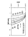
図8は、図6および図7と同様に平滑化数に応じた送信信号のPAPR特性の一例を示す。ここで、CCDF(Complementary Cumulative Distribution Function)はPAPRが所定の値以上になる確率を表している。図8では、DFT区間の平滑化数が増大するほどPAPRも増大し、位相シフトを行わない場合の特性に漸近していくことが分かる。 FIG. 8 shows an example of the PAPR characteristic of the transmission signal according to the smoothing number, as in FIGS. 6 and 7. Here, CCDF (Complementary Cumulative Distribution Function) represents the probability that the PAPR will be a predetermined value or more. In FIG. 8, it can be seen that as the number of smoothing in the DFT interval increases, the PAPR also increases, and asymptotically approaches the characteristics when no phase shift is performed.
図9は、平均化サンプル数毎のPAPR特性と位相シフト量の誤判定確率の変化を示す。図9において、従来技術で説明したように1つのDFT区間で平滑化した場合に比べて、8つのDFT区間で平滑化した場合は、位相推定精度とBER特性とが大幅に改善されることがわかる。さらに、8つのDFT区間で平滑化しただけの場合に比べて、8つのDFT区間で平滑化し、且つ、隣接するM個(図9の例ではM=2)のサブスペクトラム間の位相差が等しくなるように位相シフトを行った場合は、僅かにPAPRが増大(0.3dB程度)するが、位相の誤判定確率を大幅(1/5倍)に低減し、BER特性を大幅に改善することができる。 FIG. 9 shows changes in the PAPR characteristic and the misjudgment probability of the phase shift amount for each number of averaged samples. In FIG. 9, the phase estimation accuracy and the BER characteristics are significantly improved when smoothing is performed with 8 DFT sections as compared with the case of smoothing with one DFT section as described in the prior art. Recognize. Furthermore, compared with the case where only smoothing is performed in 8 DFT sections, the phase difference between M sub-spectrums which are smoothed in 8 DFT sections and which are adjacent (M = 2 in the example of FIG. 9) is equal. When phase shifting is performed, the PAPR slightly increases (about 0.3 dB), but the erroneous determination probability of the phase is greatly reduced (1/5 times), and the BER characteristics are greatly improved. Can do.
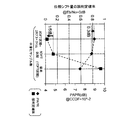
図10は、QPSK変調でサブスペクトラム数ND=16の条件における計算機シミュレーション結果の一例を示す。なお、図10は、2つのDFT区間で位相の平滑化を行い、且つ、サブスペクトラム間の平滑化を行わない場合と、2個のサブスペクトラムで位相の平滑化(M=2)を行い、且つ、複数のDFT区間での平滑化を行わない場合とにおけるPAPR特性(図10(a))およびBER特性(図10(b))を比較した結果を示す。なお、図10では、比較のために、従来技術や理論値などの各特性も示してある。 FIG. 10 shows an example of a computer simulation result under the condition of QPSK modulation and the number of subspectrums N D = 16. Note that FIG. 10 illustrates a case where the phase is smoothed in two DFT sections and the smoothing between the sub-spectrums is not performed, and the phase smoothing (M = 2) is performed in the two sub-spectrums. In addition, a result of comparing the PAPR characteristic (FIG. 10A) and the BER characteristic (FIG. 10B) when smoothing is not performed in a plurality of DFT sections is shown. In addition, in FIG. 10, each characteristic, such as a prior art and a theoretical value, is also shown for the comparison.
図10(a)の結果より、複数のDFT区間での平滑化は行わず、且つ、サブスペクトラム間の平滑化も行わない従来技術の特性Dと、複数のDFT区間での平滑化は行わず、且つ、2個のサブスペクトラムで位相を平滑化(M=2)する特性Bとを比べると、サブスペクトラム方向の平滑化によるPAPR劣化量は0.1dB程度であることが分かる。また、サブスペクトラム間の平滑化は行わず、且つ、2個のDFT区間で平滑化する特性Aと特性Bとを比べると、特性BのPAPRの方が特性Aよりも0.2dB程度多く低減されている。 From the result of FIG. 10A, smoothing in a plurality of DFT sections is not performed, and the characteristic D of the prior art that does not perform smoothing between sub-spectrums and smoothing in a plurality of DFT sections are not performed. Further, comparing with the characteristic B that smoothes the phase (M = 2) in the two sub-spectrums, it can be seen that the PAPR degradation amount due to the smoothing in the sub-spectrum direction is about 0.1 dB. Also, smoothing between sub-spectrums is not performed, and comparing the characteristics A and characteristics B smoothed in two DFT sections, the PAPR of the characteristics B is reduced by about 0.2 dB more than the characteristics A Has been.
図10(b)の結果より、複数のDFT区間での平滑化は行わず、且つ、サブスペクトラム間の平滑化も行わない従来技術の特性Dは、理論値のBER特性に比べて3dB以上劣化するが、特性Aや特性Bの位相平滑化の方法を適用することにより、BER特性が改善されることがわかる。特に、図10(b)の結果において、特性Bは、理論値の特性Cに漸近する良好な特性が得られている。 From the result of FIG. 10 (b), the characteristic D of the prior art which does not perform smoothing in a plurality of DFT sections and does not perform smoothing between sub-spectrums is deteriorated by 3 dB or more compared to the theoretical BER characteristic. However, it can be seen that the BER characteristics can be improved by applying the phase smoothing method of the characteristics A and B. In particular, in the result of FIG. 10B, the characteristic B has a good characteristic that is asymptotic to the characteristic C of the theoretical value.
上述の図10(a)および図10(b)のシミュレーション結果より、DFT方向の平滑化を行った場合(特性A)と、複数のサブスペクトラム間の平滑化を行った場合(特性B)とを比較すると、PAPRおよびPAPR特性において、特性Bの位相平滑化の方法の方が特性Aの位相平滑化の方法よりも優れた性能が得られることが分かる。
(応用例)
第1実施形態の応用例として、図1に示す送信装置50でプリアンブルを付加し、受信装置60でプリアンブルを元にしたチャネル推定を行う構成について説明する。
From the simulation results of FIG. 10A and FIG. 10B described above, when smoothing in the DFT direction is performed (characteristic A), and when smoothing between a plurality of sub-spectrums is performed (characteristic B). In the PAPR and PAPR characteristics, it is understood that the performance of the phase smoothing method of characteristic B is superior to that of the phase smoothing method of characteristic A.
(Application examples)
As an application example of the first embodiment, a configuration in which a preamble is added by the
図11は、本応用例の送信装置50aの一例を示す。なお、図11において、図1に示した送信装置50と同符号のブロックは、送信装置50と同一または同様の機能を有する。また、図1と異なる点は、加算器7−qとIDFT回路8−qとの間に、プリアンブル付加回路12−qが追加されていることと、最小PAPR信号選択器11の後にプリアンブル付加回路13が追加されていることである。
FIG. 11 shows an example of the
プリアンブル付加回路12−qは、加算器7−qが出力するスペクトラムの信号に周波数領域でプリアンブルを付加する。例えば、プリアンブル付加回路12−qは、加算器7−qが出力するスペクトラムに、振幅および位相情報が受信装置60a側で既知である(送信装置50aと受信装置60aとで事前共有している)周波数領域の波形をプリアンブルとして付加する。そして、受信装置60aは、既知の情報である振幅および位相情報と、受信したプリアンブル信号の振幅および位相の情報を比較し、比較結果から得られたひずみ特性の逆特性を受信信号に乗算することにより、伝送路における周波数領域の振幅と位相のひずみを補償することができる。
The preamble adding circuit 12-q adds a preamble in the frequency domain to the spectrum signal output from the adder 7-q. For example, in the preamble adding circuit 12-q, the amplitude and phase information are known on the receiving
プリアンブル付加回路13は、最小PAPR信号選択器11の出力信号に時間領域でプリアンブルを付加する。例えば、プリアンブル付加回路13は、時間領域における振幅および位相の情報が受信装置60a側で既知である(送信装置50aと受信装置60aとで事前共有している)時間領域の波形をプリアンブルとして付加する。そして、受信装置60aでは、既知の情報である振幅および位相の情報と、受信したプリアンブル信号の振幅および位相情報とを比較し、比較結果から得られた振幅および位相の時間的な変化量を求め、その逆特性を受信信号に乗算することにより、伝送路における時間領域の振幅と位相のひずみを補償することができる。
The
このようにして、本応用例に係る送信装置50aは、周波数領域と時間領域との両方にプリアンブルを付加して受信装置60aに送信することにあり、受信装置60aは、伝送路における時間領域の振幅と位相のひずみを補償することができる。
In this way, the
図12は、本応用例の受信装置60aの一例を示す。なお、図12において、図2に示した受信装置60と同符号のブロックは、受信装置60と同一または同様の機能を有する。また、図2と異なる点は、DFT回路21の前段にチャネル推定回路35とチャネル補償回路36とが追加されていることと、DFT回路21と抽出フィルタ22との間にチャネル推定回路37とチャネル補償回路38とが追加されていることである。
FIG. 12 shows an example of the receiving
チャネル推定回路35は、送信装置50aのプリアンブル付加回路13が時間領域で付加したプリアンブルに基づいて、伝搬路で生じる時間選択性の振幅・位相の変動量を推定し、チャネル推定値として出力する。また、チャネル推定回路35は、チャネル推定値を荷重算出器28−kにも出力し、荷重算出器28−kは、時間選択性の振幅・位相の変動量に応じた荷重を算出する。例えば、荷重算出器28−kは、時間選択性の振幅・位相の変動量が大きい場合は荷重を小さくし、逆に変動量が小さい場合は荷重を大きくする。
Based on the preamble added in the time domain by the
チャネル補償回路36は、チャネル推定回路35が推定した時間選択性の振幅・位相の変動量を補償する。そして、チャネル補償回路36が振幅・位相の変動量を補償した時間領域の信号は、DFT回路21により周波数領域のスペクトラムに変換される。
The
チャネル推定回路37では、送信装置50aのプリアンブル付加回路12−qが周波数領域で付加したプリアンブルに基づいて、伝搬路で生じる周波数選択性の振幅・位相の変動量を推定し、チャネル推定値として出力する。また、チャネル推定回路35は、チャネル推定値を荷重算出器26−kにも出力し、荷重算出器26−kは、周波数選択性の振幅・位相の変動量に応じた荷重を算出する。例えば、荷重算出器26−kは、周波数選択性の振幅・位相の変動量が大きい場合は荷重を小さくし、逆に変動量が小さい場合は荷重を大きくする。
The
チャネル補償回路38は、チャネル推定回路37が推定した周波数選択性の振幅・位相の変動量を補償する。そして、チャネル補償回路38が振幅・位相の変動量を補償した周波数領域のスペクトラムは、抽出フィルタ22−kによりND個のサブスペクトラムが抽出される。
The
このようにして、本応用例に係る受信装置60aは、送信装置50aで付加された周波数領域と時間領域との両方のプリアンブルに基づいて、伝搬路で生じる時間選択性および周波数選択性の振幅・位相の変動量を推定し、補償することができる。さらに、受信装置60aは、送信装置50aで付加された周波数領域と時間領域との両方のプリアンブルに基づいて、位相差を平滑化するときの荷重を調節するので、伝搬路で生じる時間選択性および周波数選択性の振幅・位相の変動量が大きい場合の荷重を小さくして、算出する位相差の誤差を低減することができる。
In this way, the receiving
図13は、本応用例の送信処理の一例を示す。なお、図13において、図4に示した送信処理と同符号の処理は、図4と同一または同様の処理を示す。また、図4と異なる点は、ステップ115の後に、ステップ117が追加されていることである。 FIG. 13 shows an example of the transmission process of this application example. In FIG. 13, a process having the same reference sign as the transmission process shown in FIG. 4 indicates the same or similar process as in FIG. 4. Further, the difference from FIG. 4 is that step 117 is added after step 115.
ステップS117において、送信装置50aは、位相系列θq(q=1〜C)でPAPRが最小となる信号に、時間領域および周波数領域でプリアンブルを付加して送信する。具体的には、図11で説明したように、プリアンブル付加回路12−qが周波数領域でプリアンブルを付加し、プリアンブル付加回路13が時間領域でプリアンブルを付加する。
In step S117, the
このようにして、本応用例に係る送信装置50aは、送信装置50の送信信号の周波数領域と時間領域との両方にプリアンブルを付加して受信装置60aに送信する。
In this way, the
図14は、本応用例の受信処理の一例を示す。なお、図14において、図5に示した受信処理と同符号の処理は、図5と同一または同様の処理を示す。また、図5と異なる点は、ステップ201の前に、ステップ200が追加されていることである。 FIG. 14 shows an example of reception processing of this application example. In FIG. 14, the process having the same reference sign as the reception process shown in FIG. 5 indicates the same or similar process as in FIG. 5. Further, the difference from FIG. 5 is that step 200 is added before step 201.
ステップS200において、受信装置60aは、ステップS201で分割されたスペクトラムの抽出を行う前に、伝搬路で生じた時間選択性もしくは周波数選択性の振幅・位相のチャネル変動量を推定して補償する。また、受信装置60aは、ステップS200において推定したチャネル変動量をステップS204およびステップS207で行う荷重の算出処理の参照値として出力し、ステップS204およびステップS207において、チャネル変動量に基づく荷重を算出する。
In step S200, the receiving
このようにして、本応用例に係る受信装置60aは、送信装置50aで付加された周波数領域と時間領域との両方のプリアンブルに基づいて、伝搬路で生じる時間選択性および周波数選択性の振幅・位相の変動量を推定し、補償することができる。さらに、送信装置50aで付加された周波数領域と時間領域との両方のプリアンブルに基づいて、位相差を平滑化するときの荷重を調節する。例えば、受信装置60aは、伝搬路で生じる時間選択性および周波数選択性の振幅・位相の変動量が大きい場合の荷重を小さくして、算出する位相差の誤差を低減することができる。
In this way, the receiving
以上、説明してきたように、本発明に係る通信システムおよび通信方法は、受信側における位相の推定精度を向上し、低S/N環境下や、サブスペクトラムの遷移域に存在する離散化された信号成分の数pの不足などにより劣化する受信信号のBER特性を向上することができる。 As described above, the communication system and the communication method according to the present invention improve the phase estimation accuracy on the receiving side, and are made discrete in a low S / N environment or in a sub-spectrum transition region. It is possible to improve the BER characteristic of a received signal that deteriorates due to an insufficient number p of signal components.
50,50a,150・・・送信装置;60,60a,260・・・受信装置;1,101・・・変調回路;2,102・・・波形整形フィルタ;3,21,103,211・・・DFT回路;4,104・・・分割フィルタ;5,31,105,215・・・位相器;6,23,106,213・・・周波数シフタ;7,32,107,216・・・加算器;8,33,108,217・・・IDFT回路;9,109・・・PAPR算出回路;10,27,30・・・バッファ;11,110・・・最小PAPR信号選択器;12,13・・・プリアンブル付加部;22,212・・・抽出フィルタ;24・・・位相差推定器;25,29・・・荷重付平滑化回路;26,28・・・荷重算出器;34,218・・・復調回路;35,37・・・チャネル推定回路;36,38・・・チャネル補償回路;51・・・位相系列制御装置;61・・・位相平滑化数制御装置;214・・・位相推定器
50, 50a, 150 ... transmitting device; 60, 60a, 260 ... receiving device; 1, 101 ... modulation circuit; 2, 102 ... waveform shaping filter; 3, 21, 103, 211 ... DFT circuit; 4,104: division filter; 5, 31, 105, 215 ... phase shifter; 6, 23, 106, 213 ... frequency shifter; 7, 32, 107, 216 ...
Claims (8)
前記変調部が出力する変調信号を周波数領域でN(Nは3以上の整数)個のサブスペクトラムに分割し、P個(Pは2以上の整数)に複製してP個の送信信号候補を生成する分割部と、
前記P個に複製された送信信号候補のそれぞれに対して、前記N個のサブスペクトラムを周波数軸上で分散配置する第1周波数遷移部と、
前記第1周波数遷移部が分散配置前または分散配置後の前記N個のサブスペクトラムに対して、周波数帯域が隣接するM(2≦M≦N−1の整数)個のサブスペクトラム間の位相差が等しくなるように位相シフトを行う処理および複数の時間区間で同じ位相シフトを行う処理の少なくとも一方の処理を行う第1位相部と、
分散配置および位相シフトされた前記N個のサブスペクトラムを加算した送信信号の信号電力の時間的な変動量が最小となる前記送信信号候補の信号を選択して送信する選択部と
を有する送信装置と、
受信信号から分散配置されたサブスペクトラムを抽出する抽出部と、
分散配置されたサブスペクトラムを分散配置前の周波数帯域に戻す第2周波数遷移部と、
前記抽出部が抽出した分散配置後または前記第2周波数遷移部が復元した分散配置前のサブスペクトラムに対して、周波数帯域が隣接するM個のサブスペクトラム間の重畳領域における複数の推定位相差および複数の時間区間における複数の推定位相差の少なくとも一方の推定位相差に所定の荷重を掛けて平滑化して位相補正値を算出する位相平滑化部と、
前記位相平滑化部が算出した前記位相補正値により、受信信号から抽出した分散配置後のサブスペクトラムまたは分散配置前に戻したサブスペクトラムの位相を補正する第2位相部と、
前記第2位相部が補正したN個のサブスペクトラムを加算後に時間領域の信号に変換して受信データを復調する復調部と
を有する受信装置と
を備えることを特徴とする通信システム。 A modulator for modulating transmission data;
The modulation signal output from the modulation unit is divided into N (N is an integer of 3 or more) sub-spectrums in the frequency domain, and duplicated into P (P is an integer of 2 or more) to obtain P transmission signal candidates. A dividing unit to be generated;
A first frequency transition unit that disperses and arranges the N sub-spectrums on the frequency axis for each of the P transmission signal candidates replicated;
A phase difference between M (integers of 2 ≦ M ≦ N−1) frequency bands adjacent to the N sub-spectrums before or after the first frequency transition unit is distributed. A first phase unit that performs at least one of a process of performing phase shift so as to be equal and a process of performing the same phase shift in a plurality of time intervals;
And a selection unit that selects and transmits the signal of the transmission signal candidate that minimizes the amount of temporal variation in the signal power of the transmission signal obtained by adding the N sub-spectrums that are dispersedly arranged and phase-shifted. When,
An extractor for extracting sub-spectrums distributed from the received signal;
A second frequency transition unit for returning the dispersed sub-spectrum to the frequency band before the dispersed arrangement;
A plurality of estimated phase differences in a superposed region between M sub-spectrums whose frequency bands are adjacent to each other after the dispersed arrangement extracted by the extraction unit or before the distributed arrangement restored by the second frequency transition unit, and A phase smoothing unit that calculates a phase correction value by smoothing at least one estimated phase difference of a plurality of estimated phase differences in a plurality of time intervals by applying a predetermined load;
A second phase unit that corrects the phase of the sub-spectrum after dispersion placement extracted from the received signal or the sub-spectrum returned before dispersion placement, based on the phase correction value calculated by the phase smoothing unit;
And a demodulator that demodulates received data by adding the N sub-spectrums corrected by the second phase unit to a signal in the time domain.
前記送信装置の前記選択部は、前記分割部がサブスペクトラムに逐次分割する処理を一定の時間区間毎に行う場合、u+1個(uは正の整数)の時間区間における電力の時間的な変動量を算出し、前記P個の複製信号の中から前記電力の時間的な変動量が最も小さい送信信号候補を選択して送信し、
前記受信装置の位相平滑化部は、前記抽出部が抽出した分散配置後または前記第2周波数遷移部が復元した分散配置前のサブスペクトラムに対して、隣接するサブスペクトラムの重畳領域における複数の信号成分の複数の位相差を算出し、当該複数の位相差を同じ重畳領域内で受信電力強度に応じた荷重を掛けて周波数方向の平滑化を行う処理およびu+1個の時間区間で受信電力強度に応じた荷重を掛けて時間方向の平滑化を行う処理の少なくとも一方の処理を行って前記位相補正値を算出する
ことを特徴とする通信システム。 The communication system according to claim 1,
The selection unit of the transmission device, when the division unit performs the process of sequentially dividing into sub-spectrums for each fixed time interval, temporal variation of power in u + 1 (u is a positive integer) time interval Calculating a transmission signal candidate with the smallest amount of temporal fluctuation of the power from the P replica signals, and transmitting,
The phase smoothing unit of the receiving device includes a plurality of signals in a superposed region of adjacent sub-spectrums with respect to the sub-spectrums after the dispersed placement extracted by the extracting unit or before the dispersed placement restored by the second frequency transition unit. A process of calculating a plurality of phase differences of components, applying a load corresponding to the received power intensity within the same overlapping region to smooth the frequency direction, and converting the received phase intensity into u + 1 time intervals A communication system, wherein the phase correction value is calculated by performing at least one process of performing a smoothing in a time direction by applying a corresponding load.
前記受信装置の位相平滑化部は、隣接するM個のサブスペクトラムの重畳領域の位相差を単純平均により平滑化する処理、または、受信電力強度が低い信号の荷重よりも高い信号の荷重を大きく設定してM個のサブスペクトラムの重畳領域の位相差を荷重を掛けて平滑化する処理を行って前記位相補正値を算出する
ことを特徴とする通信システム。 The communication system according to claim 1 or 2,
The phase smoothing unit of the receiving device smoothes a phase difference between adjacent M sub-spectrum overlapping regions by a simple average, or increases a signal load higher than a signal load with low received power intensity. A communication system, characterized in that the phase correction value is calculated by performing a process of setting and smoothing the phase difference of the superposed areas of the M subspectrums under a load.
前記受信装置は、伝搬路の通信チャネルで生じる周波数選択性もしくは時間選択性の振幅および位相の変動量を推定するチャネル推定部をさらに備え、
前記位相平滑化部は、前記チャネル推定部が推定する前記変動量に応じて、前記荷重を変化させて平滑化する処理を行う
ことを特徴とする通信システム。 The communication system according to any one of claims 1 to 3,
The receiving apparatus further includes a channel estimation unit that estimates the amount of variation in amplitude and phase of frequency selectivity or time selectivity generated in a communication channel of a propagation path,
The said phase smoothing part performs the process which changes and smoothes the said load according to the said variation | change_quantity estimated by the said channel estimation part. The communication system characterized by the above-mentioned.
前記P個に複製された送信信号候補のそれぞれに対して、前記N個のサブスペクトラムを周波数軸上で分散配置する処理と、
分散配置前または分散配置後の前記N個のサブスペクトラムに対して、周波数帯域が隣接するM(2≦M≦N−1の整数)個のサブスペクトラム間の位相差が等しくなるように位相シフトを行う処理および複数の時間区間で同じ位相シフトを行う処理の少なくとも一方の処理と、
分散配置および位相シフトされた前記N個のサブスペクトラムを加算した送信信号の信号電力の時間的な変動量が最小となる前記送信信号候補の信号を選択して送信する処理と
を行い、
受信装置側において、受信信号から分散配置されたサブスペクトラムを抽出する処理と、
分散配置されたサブスペクトラムを分散配置前の周波数帯域に戻す処理と、
分散配置後または復元した分散配置前のサブスペクトラムに対して、周波数帯域が隣接するM個のサブスペクトラム間の重畳領域における複数の推定位相差および複数の時間区間における複数の推定位相差の少なくとも一方の推定位相差に所定の荷重を掛けて平滑化して位相補正値を算出する処理と、
前記位相補正値により、受信信号から抽出した分散配置後のサブスペクトラムまたは分散配置前に戻したサブスペクトラムの位相を補正する処理と、
位相補正されたN個のサブスペクトラムを加算後に時間領域の信号に変換して受信データを復調する処理と
を行うことを特徴とする通信方法。 On the transmitting device side, the modulation signal is divided into N (N is an integer of 3 or more) sub-spectrums in the frequency domain, and duplicated into P (P is an integer of 2 or more) to generate P transmission signal candidates. Processing to
A process of distributing and arranging the N sub-spectrums on the frequency axis for each of the P transmitted signal candidates,
Phase shift so that the phase difference between M (an integer of 2 ≦ M ≦ N−1) adjacent frequency bands is equal to the N sub-spectrums before or after the distributed arrangement And at least one of a process for performing the same phase shift in a plurality of time intervals, and
Performing a process of selecting and transmitting the signal of the transmission signal candidate that minimizes the amount of temporal variation in the signal power of the transmission signal obtained by adding the N sub-spectrums that are dispersed and phase-shifted;
On the receiving device side, a process of extracting the sub-spectrum distributed from the received signal;
Processing to return the sub-spectrum that has been distributed to the frequency band before the distribution,
At least one of a plurality of estimated phase differences in a superposed region between M sub-spectrums whose frequency bands are adjacent to each other and a plurality of estimated phase differences in a plurality of time intervals with respect to a sub-spectrum after distributed arrangement or before restored distributed arrangement A process of calculating a phase correction value by applying a predetermined load to the estimated phase difference and smoothing,
The phase correction value corrects the phase of the subspectrum after dispersion placement extracted from the received signal or the phase of the subspectrum returned before dispersion placement;
And a process of demodulating received data by adding N sub-spectrums that have undergone phase correction to a signal in a time domain.
前記送信装置は、前記分割部がサブスペクトラムに逐次分割する処理を一定の時間区間毎に行う場合、u+1個(uは正の整数)の時間区間における電力の時間的な変動量を算出し、前記P個の複製信号の中から前記電力の時間的な変動量が最も小さい送信信号候補を選択して送信する処理を行い、
前記受信装置は、分散配置後または復元した分散配置前のサブスペクトラムに対して、隣接するサブスペクトラムの重畳領域における複数の信号成分の複数の位相差を算出し、当該複数の位相差を同じ重畳領域内で受信電力強度に応じた荷重を掛けて周波数方向の平滑化を行う処理およびu+1個の時間区間で受信電力強度に応じた荷重を掛けて時間方向の平滑化を行う処理の少なくとも一方の処理を行って前記位相補正値を算出する処理を行う
ことを特徴とする通信方法。 The communication method according to claim 5, wherein
When the transmission unit performs the process of sequentially dividing the sub-spectrum into sub-spectrums for each fixed time interval, the transmission device calculates a temporal variation amount of power in u + 1 (u is a positive integer) time interval, Performing a process of selecting and transmitting a transmission signal candidate having the smallest amount of temporal variation of the power from the P replica signals;
The receiving apparatus calculates a plurality of phase differences of a plurality of signal components in a superimposed region of adjacent sub-spectrums after the dispersed arrangement or before the restored dispersed arrangement, and the plurality of phase differences are superimposed on the same At least one of processing for smoothing in the frequency direction by applying a load corresponding to the received power intensity in the region and processing for smoothing in the time direction by applying a load corresponding to the received power intensity in u + 1 time intervals A communication method comprising: performing a process to calculate the phase correction value.
前記受信装置は、隣接するM個のサブスペクトラムの重畳領域の位相差を単純平均により平滑化する処理、または、受信電力強度が低い信号の荷重よりも高い信号の荷重を大きく設定してM個のサブスペクトラムの重畳領域の位相差に荷重を掛けて平滑化する処理を行って前記位相補正値を算出する
ことを特徴とする通信方法。 The communication method according to claim 5 or 6,
The receiving apparatus performs processing for smoothing the phase difference between the overlapping regions of the M sub-spectrums adjacent to each other by a simple average, or sets the signal load higher than the signal load with low received power intensity to M A communication method characterized by calculating a phase correction value by performing a process of applying a load to the phase difference in the superspected region of the sub-spectrum and smoothing it.
前記受信装置は、伝搬路の通信チャネルで生じる周波数選択性もしくは時間選択性の振幅および位相の変動量を推定し、前記変動量に応じて、前記荷重を変化させて平滑化する処理を行う
ことを特徴とする通信方法。 The communication method according to any one of claims 5 to 7,
The receiving apparatus estimates a frequency-selective or time-selective amplitude and phase fluctuation amount that occurs in a communication channel of a propagation path, and performs a process of changing and smoothing the load according to the fluctuation amount. A communication method characterized by the above.
Priority Applications (1)
| Application Number | Priority Date | Filing Date | Title |
|---|---|---|---|
| JP2016023958A JP6426637B2 (en) | 2016-02-10 | 2016-02-10 | Communication system and communication method |
Applications Claiming Priority (1)
| Application Number | Priority Date | Filing Date | Title |
|---|---|---|---|
| JP2016023958A JP6426637B2 (en) | 2016-02-10 | 2016-02-10 | Communication system and communication method |
Publications (2)
| Publication Number | Publication Date |
|---|---|
| JP2017143433A true JP2017143433A (en) | 2017-08-17 |
| JP6426637B2 JP6426637B2 (en) | 2018-11-21 |
Family
ID=59627482
Family Applications (1)
| Application Number | Title | Priority Date | Filing Date |
|---|---|---|---|
| JP2016023958A Active JP6426637B2 (en) | 2016-02-10 | 2016-02-10 | Communication system and communication method |
Country Status (1)
| Country | Link |
|---|---|
| JP (1) | JP6426637B2 (en) |
Cited By (2)
| Publication number | Priority date | Publication date | Assignee | Title |
|---|---|---|---|---|
| JP2017220725A (en) * | 2016-06-03 | 2017-12-14 | 日本電信電話株式会社 | Communication system and communication method |
| JP2020123788A (en) * | 2019-01-29 | 2020-08-13 | 日本電信電話株式会社 | Spectrum division transmission system, spectrum division transmission method, transmitter, and receiver |
Citations (4)
| Publication number | Priority date | Publication date | Assignee | Title |
|---|---|---|---|---|
| WO2012049912A1 (en) * | 2010-10-14 | 2012-04-19 | 三菱電機株式会社 | Transmitter apparatus, receiver apparatus and relay apparatus |
| JP2012191377A (en) * | 2011-03-10 | 2012-10-04 | Nippon Telegr & Teleph Corp <Ntt> | Receiver |
| WO2012176495A1 (en) * | 2011-06-22 | 2012-12-27 | 三菱電機株式会社 | Transmitter apparatus, receiver apparatus, communication system and communication method |
| JP2014017609A (en) * | 2012-07-06 | 2014-01-30 | Nippon Telegr & Teleph Corp <Ntt> | Receiving device and receiving method |
-
2016
- 2016-02-10 JP JP2016023958A patent/JP6426637B2/en active Active
Patent Citations (4)
| Publication number | Priority date | Publication date | Assignee | Title |
|---|---|---|---|---|
| WO2012049912A1 (en) * | 2010-10-14 | 2012-04-19 | 三菱電機株式会社 | Transmitter apparatus, receiver apparatus and relay apparatus |
| JP2012191377A (en) * | 2011-03-10 | 2012-10-04 | Nippon Telegr & Teleph Corp <Ntt> | Receiver |
| WO2012176495A1 (en) * | 2011-06-22 | 2012-12-27 | 三菱電機株式会社 | Transmitter apparatus, receiver apparatus, communication system and communication method |
| JP2014017609A (en) * | 2012-07-06 | 2014-01-30 | Nippon Telegr & Teleph Corp <Ntt> | Receiving device and receiving method |
Non-Patent Citations (2)
| Title |
|---|
| 宮武遼 他: "帯域分散伝送におけるSLM方式適用時の位相系推定特性向上の検討", 電子情報通信学会2015年通信ソサイエティ大会講演論文集1, JPN6018040508, 25 August 2015 (2015-08-25), pages 187, ISSN: 0003899168 * |
| 宮武遼 他: "帯域分散伝送方式におけるPAPR低減に関する一検討", 電子情報通信学会2015年総合大会講演論文集 通信1, JPN6018040510, 24 February 2015 (2015-02-24), pages 274, ISSN: 0003899169 * |
Cited By (3)
| Publication number | Priority date | Publication date | Assignee | Title |
|---|---|---|---|---|
| JP2017220725A (en) * | 2016-06-03 | 2017-12-14 | 日本電信電話株式会社 | Communication system and communication method |
| JP2020123788A (en) * | 2019-01-29 | 2020-08-13 | 日本電信電話株式会社 | Spectrum division transmission system, spectrum division transmission method, transmitter, and receiver |
| JP7140333B2 (en) | 2019-01-29 | 2022-09-21 | 日本電信電話株式会社 | Spectrum division transmission system, spectrum division transmission method, transmitter and receiver |
Also Published As
| Publication number | Publication date |
|---|---|
| JP6426637B2 (en) | 2018-11-21 |
Similar Documents
| Publication | Publication Date | Title |
|---|---|---|
| CN101433038B (en) | The distribution of uplink reference signals | |
| US8351532B2 (en) | Iterative interference cancellation | |
| US7443827B2 (en) | Mobile communication system, multicarrier CDMA transmitter, and multicarrier CDMA receiver | |
| JP4413232B2 (en) | Channel evaluator and method for evaluating channel transfer function, and apparatus and method for supplying pilot sequence | |
| EP1875694B1 (en) | Reduced complexity channel estimation in ofdm systems | |
| EP3342084B1 (en) | Apparatus and method for generating and using a pilot signal | |
| EP1974487B1 (en) | Mc-cdma system, transmitter and receiver | |
| EP3738280A1 (en) | Ofdm signal and noise estimation | |
| JP5014293B2 (en) | MIMO-OFDM receiver | |
| JP2017143433A (en) | Communication system and communication method | |
| JP2009049491A (en) | Receiving apparatus, receiving method, and program | |
| TWI499251B (en) | Carrier and sampling frequency offsets estimating method and associated apparatus applied to multi-carrier communication system | |
| WO2010049508A1 (en) | Receiver with channel estimation circuitry | |
| JP5047391B2 (en) | Receiving apparatus and receiving method | |
| JP5645613B2 (en) | Wireless communication system, transmitter and receiver | |
| JP3495962B2 (en) | Distortion estimation device | |
| JP6498523B2 (en) | COMMUNICATION METHOD, COMMUNICATION SYSTEM, AND COMMUNICATION DEVICE | |
| KR100899139B1 (en) | Receiver for Frame Synchronization in Wireless Communication Systems and Method thereof | |
| EP2328310B1 (en) | Method for estimating a received signal and corresponding device | |
| KR20170089738A (en) | Method and apparatus for estmating and correcting phase error in a wireless communication system | |
| KR100768327B1 (en) | Apparatus and method for estimating carrier to interference and noise ratio in systems using multi-carrier signal | |
| CN113452404B (en) | Multi-carrier spread spectrum capturing method and device, electronic equipment and storage medium | |
| KR20070018663A (en) | Apparatus and method for estimating carrier-to-interference noise ratio in an ofdm communication system | |
| US9667448B2 (en) | Method and apparatus for channel estimation in wireless communication system | |
| CN111884979B (en) | OFDM smart grid impulse noise resistant symbol synchronization method |
Legal Events
| Date | Code | Title | Description |
|---|---|---|---|
| A621 | Written request for application examination |
Free format text: JAPANESE INTERMEDIATE CODE: A621 Effective date: 20171218 |
|
| A977 | Report on retrieval |
Free format text: JAPANESE INTERMEDIATE CODE: A971007 Effective date: 20181011 |
|
| TRDD | Decision of grant or rejection written | ||
| A01 | Written decision to grant a patent or to grant a registration (utility model) |
Free format text: JAPANESE INTERMEDIATE CODE: A01 Effective date: 20181023 |
|
| A61 | First payment of annual fees (during grant procedure) |
Free format text: JAPANESE INTERMEDIATE CODE: A61 Effective date: 20181025 |
|
| R150 | Certificate of patent or registration of utility model |
Ref document number: 6426637 Country of ref document: JP Free format text: JAPANESE INTERMEDIATE CODE: R150 |