JP2017143228A - Imprint device, and method of manufacturing article - Google Patents
Imprint device, and method of manufacturing article Download PDFInfo
- Publication number
- JP2017143228A JP2017143228A JP2016025201A JP2016025201A JP2017143228A JP 2017143228 A JP2017143228 A JP 2017143228A JP 2016025201 A JP2016025201 A JP 2016025201A JP 2016025201 A JP2016025201 A JP 2016025201A JP 2017143228 A JP2017143228 A JP 2017143228A
- Authority
- JP
- Japan
- Prior art keywords
- substrate
- imprint material
- imprint
- discharge port
- mold
- Prior art date
- Legal status (The legal status is an assumption and is not a legal conclusion. Google has not performed a legal analysis and makes no representation as to the accuracy of the status listed.)
- Granted
Links
Images


Classifications
-
- G—PHYSICS
- G03—PHOTOGRAPHY; CINEMATOGRAPHY; ANALOGOUS TECHNIQUES USING WAVES OTHER THAN OPTICAL WAVES; ELECTROGRAPHY; HOLOGRAPHY
- G03F—PHOTOMECHANICAL PRODUCTION OF TEXTURED OR PATTERNED SURFACES, e.g. FOR PRINTING, FOR PROCESSING OF SEMICONDUCTOR DEVICES; MATERIALS THEREFOR; ORIGINALS THEREFOR; APPARATUS SPECIALLY ADAPTED THEREFOR
- G03F7/00—Photomechanical, e.g. photolithographic, production of textured or patterned surfaces, e.g. printing surfaces; Materials therefor, e.g. comprising photoresists; Apparatus specially adapted therefor
- G03F7/16—Coating processes; Apparatus therefor
-
- B—PERFORMING OPERATIONS; TRANSPORTING
- B05—SPRAYING OR ATOMISING IN GENERAL; APPLYING FLUENT MATERIALS TO SURFACES, IN GENERAL
- B05D—PROCESSES FOR APPLYING FLUENT MATERIALS TO SURFACES, IN GENERAL
- B05D3/00—Pretreatment of surfaces to which liquids or other fluent materials are to be applied; After-treatment of applied coatings, e.g. intermediate treating of an applied coating preparatory to subsequent applications of liquids or other fluent materials
- B05D3/12—Pretreatment of surfaces to which liquids or other fluent materials are to be applied; After-treatment of applied coatings, e.g. intermediate treating of an applied coating preparatory to subsequent applications of liquids or other fluent materials by mechanical means
-
- B—PERFORMING OPERATIONS; TRANSPORTING
- B29—WORKING OF PLASTICS; WORKING OF SUBSTANCES IN A PLASTIC STATE IN GENERAL
- B29C—SHAPING OR JOINING OF PLASTICS; SHAPING OF MATERIAL IN A PLASTIC STATE, NOT OTHERWISE PROVIDED FOR; AFTER-TREATMENT OF THE SHAPED PRODUCTS, e.g. REPAIRING
- B29C43/00—Compression moulding, i.e. applying external pressure to flow the moulding material; Apparatus therefor
- B29C43/32—Component parts, details or accessories; Auxiliary operations
- B29C43/58—Measuring, controlling or regulating
-
- G—PHYSICS
- G03—PHOTOGRAPHY; CINEMATOGRAPHY; ANALOGOUS TECHNIQUES USING WAVES OTHER THAN OPTICAL WAVES; ELECTROGRAPHY; HOLOGRAPHY
- G03F—PHOTOMECHANICAL PRODUCTION OF TEXTURED OR PATTERNED SURFACES, e.g. FOR PRINTING, FOR PROCESSING OF SEMICONDUCTOR DEVICES; MATERIALS THEREFOR; ORIGINALS THEREFOR; APPARATUS SPECIALLY ADAPTED THEREFOR
- G03F7/00—Photomechanical, e.g. photolithographic, production of textured or patterned surfaces, e.g. printing surfaces; Materials therefor, e.g. comprising photoresists; Apparatus specially adapted therefor
- G03F7/0002—Lithographic processes using patterning methods other than those involving the exposure to radiation, e.g. by stamping
-
- H—ELECTRICITY
- H01—ELECTRIC ELEMENTS
- H01L—SEMICONDUCTOR DEVICES NOT COVERED BY CLASS H10
- H01L21/00—Processes or apparatus adapted for the manufacture or treatment of semiconductor or solid state devices or of parts thereof
- H01L21/02—Manufacture or treatment of semiconductor devices or of parts thereof
- H01L21/027—Making masks on semiconductor bodies for further photolithographic processing not provided for in group H01L21/18 or H01L21/34
- H01L21/0271—Making masks on semiconductor bodies for further photolithographic processing not provided for in group H01L21/18 or H01L21/34 comprising organic layers
-
- B—PERFORMING OPERATIONS; TRANSPORTING
- B29—WORKING OF PLASTICS; WORKING OF SUBSTANCES IN A PLASTIC STATE IN GENERAL
- B29C—SHAPING OR JOINING OF PLASTICS; SHAPING OF MATERIAL IN A PLASTIC STATE, NOT OTHERWISE PROVIDED FOR; AFTER-TREATMENT OF THE SHAPED PRODUCTS, e.g. REPAIRING
- B29C43/00—Compression moulding, i.e. applying external pressure to flow the moulding material; Apparatus therefor
- B29C43/32—Component parts, details or accessories; Auxiliary operations
- B29C43/34—Feeding the material to the mould or the compression means
- B29C2043/3433—Feeding the material to the mould or the compression means using dispensing heads, e.g. extruders, placed over or apart from the moulds
-
- B—PERFORMING OPERATIONS; TRANSPORTING
- B29—WORKING OF PLASTICS; WORKING OF SUBSTANCES IN A PLASTIC STATE IN GENERAL
- B29C—SHAPING OR JOINING OF PLASTICS; SHAPING OF MATERIAL IN A PLASTIC STATE, NOT OTHERWISE PROVIDED FOR; AFTER-TREATMENT OF THE SHAPED PRODUCTS, e.g. REPAIRING
- B29C43/00—Compression moulding, i.e. applying external pressure to flow the moulding material; Apparatus therefor
- B29C43/32—Component parts, details or accessories; Auxiliary operations
- B29C43/58—Measuring, controlling or regulating
- B29C2043/585—Measuring, controlling or regulating detecting defects, e.g. foreign matter between the moulds, inaccurate position, breakage
-
- B—PERFORMING OPERATIONS; TRANSPORTING
- B29—WORKING OF PLASTICS; WORKING OF SUBSTANCES IN A PLASTIC STATE IN GENERAL
- B29C—SHAPING OR JOINING OF PLASTICS; SHAPING OF MATERIAL IN A PLASTIC STATE, NOT OTHERWISE PROVIDED FOR; AFTER-TREATMENT OF THE SHAPED PRODUCTS, e.g. REPAIRING
- B29C43/00—Compression moulding, i.e. applying external pressure to flow the moulding material; Apparatus therefor
- B29C43/32—Component parts, details or accessories; Auxiliary operations
- B29C43/58—Measuring, controlling or regulating
- B29C2043/5875—Measuring, controlling or regulating the material feed to the moulds or mould parts, e.g. controlling feed flow, velocity, weight, doses
- B29C2043/5883—Measuring, controlling or regulating the material feed to the moulds or mould parts, e.g. controlling feed flow, velocity, weight, doses ensuring cavity filling, e.g. providing overflow means
-
- B—PERFORMING OPERATIONS; TRANSPORTING
- B29—WORKING OF PLASTICS; WORKING OF SUBSTANCES IN A PLASTIC STATE IN GENERAL
- B29C—SHAPING OR JOINING OF PLASTICS; SHAPING OF MATERIAL IN A PLASTIC STATE, NOT OTHERWISE PROVIDED FOR; AFTER-TREATMENT OF THE SHAPED PRODUCTS, e.g. REPAIRING
- B29C43/00—Compression moulding, i.e. applying external pressure to flow the moulding material; Apparatus therefor
- B29C43/02—Compression moulding, i.e. applying external pressure to flow the moulding material; Apparatus therefor of articles of definite length, i.e. discrete articles
- B29C43/18—Compression moulding, i.e. applying external pressure to flow the moulding material; Apparatus therefor of articles of definite length, i.e. discrete articles incorporating preformed parts or layers, e.g. compression moulding around inserts or for coating articles
-
- B—PERFORMING OPERATIONS; TRANSPORTING
- B29—WORKING OF PLASTICS; WORKING OF SUBSTANCES IN A PLASTIC STATE IN GENERAL
- B29C—SHAPING OR JOINING OF PLASTICS; SHAPING OF MATERIAL IN A PLASTIC STATE, NOT OTHERWISE PROVIDED FOR; AFTER-TREATMENT OF THE SHAPED PRODUCTS, e.g. REPAIRING
- B29C43/00—Compression moulding, i.e. applying external pressure to flow the moulding material; Apparatus therefor
- B29C43/32—Component parts, details or accessories; Auxiliary operations
- B29C43/34—Feeding the material to the mould or the compression means
Landscapes
- Engineering & Computer Science (AREA)
- Mechanical Engineering (AREA)
- Physics & Mathematics (AREA)
- General Physics & Mathematics (AREA)
- Condensed Matter Physics & Semiconductors (AREA)
- Manufacturing & Machinery (AREA)
- Computer Hardware Design (AREA)
- Microelectronics & Electronic Packaging (AREA)
- Power Engineering (AREA)
- Shaping Of Tube Ends By Bending Or Straightening (AREA)
- Exposure Of Semiconductors, Excluding Electron Or Ion Beam Exposure (AREA)
Abstract
Description
本発明は、インプリント装置、及び物品の製造方法に関する。 The present invention relates to an imprint apparatus and an article manufacturing method.
インプリント技術は、ナノスケールの微細パターンの転写を可能にする技術であり、半導体デバイスや磁気記憶媒体の量産用ナノリソグラフィ技術の1つとして注目されている。インプリント技術を用いたインプリント装置では、インプリント材の基板上における供給位置を示すマップ(インプリントレシピやドロップレシピとも呼ばれる)に基づいて、インプリント材が基板上に供給される。そして、パターンが形成されたモールドと基板上に供給されたインプリント材とを接触させた状態でインプリント材を硬化させ、硬化したインプリント材からモールドを引き離すことで基板上にパターンを形成する。 The imprint technique is a technique that enables transfer of a nanoscale fine pattern, and has attracted attention as one of nanolithography techniques for mass production of semiconductor devices and magnetic storage media. In an imprint apparatus using an imprint technique, an imprint material is supplied onto a substrate based on a map (also referred to as an imprint recipe or a drop recipe) indicating a supply position of the imprint material on the substrate. Then, the imprint material is cured in a state where the mold on which the pattern is formed and the imprint material supplied on the substrate are in contact with each other, and the pattern is formed on the substrate by separating the mold from the cured imprint material. .
インプリント装置には、基板上に形成されるパターンの欠陥(未充填欠陥、残膜厚(RLT)の異常、等)を低減することが求められている。インプリント材は、インプリント装置が備えるディスペンサなどの供給部から基板上に供給されるが、インプリント材を吐出する吐出口が詰まることがある。特定の吐出口からインプリント材が吐出されない場合、基板上に供給すべきインプリント材の一部が欠けてしまうため、かかる箇所でパターンの欠陥が発生しうる。 The imprint apparatus is required to reduce the defects (unfilled defects, residual film thickness (RLT) abnormality, etc.) of the pattern formed on the substrate. The imprint material is supplied onto the substrate from a supply unit such as a dispenser provided in the imprint apparatus, but a discharge port for discharging the imprint material may be clogged. When the imprint material is not discharged from a specific discharge port, a part of the imprint material to be supplied onto the substrate is lost, and thus a pattern defect may occur at such a location.
そこで、インプリント材の液滴を吐出する際のインクジェット法における主走査方向とモールドのパターンのライン方向とで規定される交差角度が30度から90度になるように、インプリント材の液滴を供給する技術が提案されている(特許文献1参照)。 Therefore, the droplets of the imprint material are set so that the intersecting angle defined by the main scanning direction and the line direction of the mold pattern in the ink jet method when discharging the droplets of the imprint material is 30 degrees to 90 degrees. Has been proposed (see Patent Document 1).
しかしながら、特許文献1に開示された技術では、インプリント材を吐出することができない吐出口の影響は軽減されるものの、基板上に形成されるパターンにおける欠陥の軽減は十分とはいえない。
However, with the technique disclosed in
本発明は、正確なパターン形成に有利なインプリント装置を提供することを例示的目的とする。 An object of the present invention is to provide an imprint apparatus advantageous for accurate pattern formation.
上記目的を達成するために、本発明の一側面としてのインプリント装置は、基板上のインプリント材を成型してパターンを形成するインプリント装置であって、インプリント材を吐出する複数の吐出口を含み、前記インプリント材を基板上に供給する供給部と、前記複数の吐出口のうちに異常な吐出口が存在する場合、前記複数の吐出口のうち前記異常な吐出口とは別の吐出口に前記インプリント材を吐出させるように、前記供給部を制御する制御部と、を有することを特徴とする。 In order to achieve the above object, an imprint apparatus according to one aspect of the present invention is an imprint apparatus that forms a pattern by molding an imprint material on a substrate, and includes a plurality of discharges that discharge the imprint material. A supply unit that includes an outlet and supplies the imprint material onto the substrate; and when there is an abnormal discharge port among the plurality of discharge ports, the abnormal discharge port is different from the plurality of discharge ports. And a control unit for controlling the supply unit so that the imprint material is discharged to the discharge port.
本発明の更なる目的又はその他の側面は、以下、添付図面を参照して説明される好ましい実施形態によって明らかにされるであろう。 Further objects and other aspects of the present invention will become apparent from the preferred embodiments described below with reference to the accompanying drawings.
本発明によれば、例えば、正確なパターン形成に有利なインプリント装置を提供することができる。 According to the present invention, for example, an imprint apparatus that is advantageous for accurate pattern formation can be provided.
以下、添付図面を参照して、本発明の好適な実施の形態について説明する。なお、各図において、同一の部材については同一の参照番号を付し、重複する説明は省略する。 DESCRIPTION OF EXEMPLARY EMBODIMENTS Hereinafter, preferred embodiments of the invention will be described with reference to the accompanying drawings. In addition, in each figure, the same reference number is attached | subjected about the same member and the overlapping description is abbreviate | omitted.
<第1実施形態>
図1は、本発明の一側面としてのインプリント装置100の構成を示す概略図である。インプリント装置100は、半導体デバイスなどの製造プロセスで使用されるリソグラフィ装置である。インプリント装置100は、基板上のインプリント材を成型してパターンを形成するインプリント処理を行う。
<First Embodiment>
FIG. 1 is a schematic diagram illustrating a configuration of an
本実施形態では、インプリント材として光硬化性の樹脂材料を想定し、光(紫外線など)の照射によってインプリント材を硬化させる光硬化法を採用する。但し、本発明は、インプリント材を樹脂材料に限定するものではなく、例えば、無機材料の粉末や粒子を含む光硬化性の材料などであってもよい。また、インプリント材の硬化法も光硬化法に限定するものではなく、例えば、熱によってインプリント材を硬化させる熱硬化法を採用してもよい。 In this embodiment, a photo-curing resin material is assumed as the imprint material, and a photo-curing method is adopted in which the imprint material is cured by irradiation with light (such as ultraviolet rays). However, the present invention does not limit the imprint material to a resin material, and may be, for example, a photocurable material containing powder or particles of an inorganic material. Further, the curing method of the imprint material is not limited to the photocuring method, and for example, a thermosetting method in which the imprint material is cured by heat may be employed.
インプリント装置100は、図1に示すように、基板101を保持するステージ102と、モールド103を保持するヘッド104と、収容部106と、吐出部107と、格納部108と、照射部109と、観察部110と、制御部111とを有する。また、以下では、基板上のインプリント材に対して光を照射する照射部109の光軸に沿った方向をZ軸とし、Z軸に垂直な平面内において互いに直交する方向をX軸及びY軸とする。
As illustrated in FIG. 1, the
基板101は、モールド103のパターンが転写される基板であって、例えば、単結晶シリコン基板やSOI(Silicon on Insulator)基板などを含む。
The
ステージ102は、基板101を保持する基板チャックと、モールド103と基板101との位置合わせ(アライメント)を行うための駆動機構とを含む。かかる駆動機構は、例えば、粗動駆動系と微動駆動系とを含み、X軸方向及びY軸方向に基板101を駆動する(移動させる)。また、かかる駆動機構は、X軸方向及びY軸方向だけではなく、Z軸方向及びθ(Z軸周りの回転)方向に基板101を駆動する機能や基板101の傾きを補正するためのチルト機能を備えていてもよい。ステージ102は、本実施形態において、吐出部107における複数の吐出口と基板101との相対位置を変更する機能を実現する。
The
モールド103は、成型のための型であって、基板101に対向する面に、基板101に供給されたインプリント材105に転写すべきパターンが形成されたパターン領域を有する。モールド103は、本実施形態では、ラインパターン(ライン状の凹凸の溝)をパターン領域に含む。モールド103は、例えば、矩形の外形形状を有する。モールド103は、基板上のインプリント材105を硬化させるための光、本実施形態では、紫外線を透過する材料、例えば、石英などで構成されている。
The
ヘッド104は、モールド103を真空吸引力又は静電気力によって保持(固定)する。ヘッド104は、モールド103をZ軸方向に駆動する(移動させる)駆動機構を含む。ヘッド104は、基板上に供給された未硬化のインプリント材105にモールド103を押印する機能、及び、基板上の硬化したインプリント材105からモールド103を引き離す機能を有する。
The
収容部106と、未硬化のインプリント材105を収容(保管)するタンクを含む。収容部106は、供給管を介して、吐出部107に対して未硬化のインプリント材105を供給する。なお、収容部106は、吐出部107に対して、構造的に分離していてもよいし、一体となっていてもよい。
The
吐出部107は、例えば、基板101に対してインプリント材105の液滴を吐出する複数の吐出口(ノズル)を含むディスペンサで構成され、基板上にインプリント材105を供給(塗布)する供給部として機能する。吐出部107におけるインプリント材105の供給量の単位は、ここでは「滴」であり、インプリント材105の1滴あたりの量は、サブピコリットルから数ピコリットルとしうる。なお、吐出部107は、基板上の単位領域ごとに予め定めた量のインプリント材105を供給するものであればよく、インプリント材105を当該単位領域に液滴として飛来させる必要はない。
For example, the
吐出部107からインプリント材105の液滴を滴下可能な基板上の位置(供給位置)は、吐出口の配列方向に関しては、吐出口の物理的な間隔に依存し、数μmから数10μmごとと決まる。また、吐出部107からインプリント材105の液滴を滴下可能な基板上の位置は、吐出口に対して基板101を走査する走査方向(吐出口の配列方向に直交する方向)に関しては、インプリント材105の吐出周期及びステージ102の速度によって決まる。
The position (supply position) on the substrate where droplets of the
収容部106から吐出部107にインプリント材105を供給するとともに、ステージ102を走査方向に駆動しながら吐出部107からインプリント材105の液滴を吐出することで、基板上にインプリント材105の液滴の配列が形成される。
The
格納部108は、基板上に形成すべきインプリント材105の液滴の配列、即ち、インプリント材105の液滴の供給位置を示すマップ(インプリントレシピ又はドロップレシピ)を格納する。マップは、後述するように、基板上における吐出部107の複数の吐出口のそれぞれの位置に関連付けられて基板上に規定される座標系でのインプリント材105の液滴の供給位置に関する座標データを含む。また、マップは、インプリント材105の液滴を吐出する際に用いる吐出口を識別するための吐出口番号データも含むことができる。なお、マップは、画像形式であってもテキスト形式であってもよいし、これらの組み合わせであってもよい。
The
マップは、インプリント装置100に関する種々の情報のうちの少なくとも1つに基づいて、基板上に形成されるインプリント材105のパターンの欠陥や残膜厚の異常を抑えるように生成されている。ここで、インプリント装置100に関する種々の情報は、例えば、基板101に関する情報、モールド103に関する情報、インプリント材105に関する情報、吐出部107に関する情報、インプリント条件に関する情報、装置条件に関する情報を含む。基板101に関する情報は、例えば、基板101の最表面層の濡れ性やトポグラフィなどを含む。モールド103に関する情報は、モールド103のパターンのレイアウト、ピッチ、形状及び深さやモールド103の使用履歴などを含む。インプリント材105に関する情報は、インプリント材105の粘度、表面エネルギー及び揮発量などを含む。吐出部107に関する情報は、1つの吐出口から吐出されるインプリント材105の1つの液滴の体積量、吐出口の間隔、吐出周期などを含む。インプリント条件に関する情報は、基板101に形成すべきインプリント材105のパターンの残膜厚の設計値、モールド103のパターンへのインプリント材105の充填時間などを含む。装置条件に関する情報は、ステージ102の速度、照射部109の照度、気流条件(インプリント装置100に供給されるガスの種類、流量及び方向)などを含む。
The map is generated based on at least one of various types of information regarding the
照射部109は、基板上のインプリント材105を硬化させる機能を有する。照射部109は、例えば、ハロゲンランプやLEDなどを含み、モールド103を介して、基板上のインプリント材105に紫外線を照射する。
The
観察部110は、例えば、カメラを含み、モールド103を介して基板101を観察する。具体的には、観察部110は、吐出部107から吐出されて基板上に供給されたインプリント材105の状態を観察する。ここで、基板上に供給されたインプリント材105の状態とは、基板上に形成されたインプリント材105の液滴の配列やモールド103と基板上のインプリント材105とを接触させた状態におけるインプリント材105の広がりなどを含む。観察部110は、吐出部107から基板上にインプリント材105を供給してから基板上の硬化したインプリント材105からモールド103を引き離すまでの期間において、インプリント材105の充填状況や異物の有無を観察することが可能である。
The
制御部111は、CPUやメモリなどを含み、インプリント装置100の全体(動作)を制御する。制御部111は、インプリント装置100の各部を制御して、インプリント処理を行う。また、本実施形態において、制御部111は、格納部108に格納されているマップを更新する機能や吐出部107における複数の吐出口と基板101との相対位置を制御(変更)する機能を実現する。
The
インプリント装置100においては、マップに基づいて、吐出部107から基板上にインプリント材105の液滴を供給する。そして、モールド103と基板上のインプリント材105とを接触させた状態でインプリント材105を硬化させ、硬化したインプリント材105からモールド103を引き離す(離型する)ことで基板上にインプリント材105のパターンを形成する。
In the
図2は、インプリント装置100におけるインプリント処理を説明するためのフローチャートである。インプリント処理は、上述したように、制御部111がインプリント装置100の各部を統括的に制御することで行われる。
FIG. 2 is a flowchart for explaining imprint processing in the
S100では、基板101に形成すべきパターンを形成可能なモールド103をインプリント装置100に搬入し、かかるモールド103をヘッド104に保持させる。モールド103は、例えば、フォトマスクに用いる透明な石英基板に、設計情報に対応する凹凸のパターンが形成されたものである。
In S <b> 100, a
S101では、基板101をインプリント装置100に搬入し、かかる基板101をステージ102に保持させる。
In step S <b> 101, the
S102では、格納部108に格納されている複数のマップからインプリント処理に用いる1つのマップを選択する。例えば、モールド103に関する情報、基板101に関する情報、インプリント材105に関する情報、吐出部107に関する情報、インプリント条件に関する情報及び装置条件に関する情報のうちの少なくとも1つに基づいて、マップを選択する。かかるマップは、目標とする充填時間に対して、欠陥や残膜厚の異常のないインプリント処理が可能なように、且つ、最短の時間で必要な特性が得られるように最適化されている。S102で選択したマップが示す基板上の供給位置にインプリント材105が供給されることが最もよい。
In S102, one map used for imprint processing is selected from a plurality of maps stored in the storage unit. For example, the map is selected based on at least one of information on the
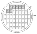
S103では、図3に示す基板上のショット領域のうち、インプリント処理が行われていないショット領域を対象ショット領域として指定する。ここで、ショット領域とは、1回のインプリント処理でパターンが形成される領域を意味するものとする。本実施形態では、例えば、図3に示すように、基板101において連続するショット領域S1、S2、S3、・・・S41、S42の順にインプリント処理を行う。但し、インプリント処理の順序は、図3に示すようなものに限定されるものではなく、千鳥格子順であってもよいし、ランダムであってもよい。 In S103, a shot area that has not been subjected to imprint processing among the shot areas on the substrate shown in FIG. 3 is designated as the target shot area. Here, the shot area means an area where a pattern is formed by one imprint process. In the present embodiment, for example, as shown in FIG. 3, imprint processing is performed in the order of continuous shot regions S1, S2, S3,. However, the order of the imprint process is not limited to that shown in FIG. 3, and may be a houndstooth order or a random order.
S104では、吐出部107によって、基板上にインプリント材105を供給する。この際、吐出部107は、図4(a)に示すように、S102で選択されたマップに従って、ステージ102の移動に応じて基板上にインプリント材105の液滴を順次吐出する。
In S104, the
S105では、押印処理を行う。具体的には、まず、図4(b)に示すように、インプリント材105が供給された基板101に対して、モールド103を近接させる。次いで、図4(c)に示すように、モールド103と基板101との位置合わせを行いながら、モールド103と基板上のインプリント材105とを接触させる。そして、モールド103のパターンにインプリント材105が充填されるまで、かかる状態を維持する。モールド103と基板上のインプリント材105とを接触させた初期段階では、モールド103のパターンへのインプリント材105の充填が不十分であるため、パターンの一部(隅)に充填欠陥を生じている。但し、モールド103と基板上のインプリント材105とを接触させた状態で時間が経過していくにつれて、モールド103のパターンの隅々までインプリント材105が充填され、充填欠陥が減少する。
In S105, a stamping process is performed. Specifically, first, as shown in FIG. 4B, the
S106では、硬化処理を行う。具体的には、モールド103のパターンにインプリント材105を十分充填させた後、図4(d)に示すように、照射部109によって、モールド103の裏面からインプリント材105に紫外線を所定時間照射して、基板上のインプリント材105を硬化させる。
In S106, a curing process is performed. Specifically, after the pattern of the
S107では、離型処理を行う。具体的には、図4(e)に示すように、基板上の硬化したインプリント材105からモールド103を引き離す。これにより、基板上にモールド103のパターンに対応するインプリント材105のパターンが形成される。
In S107, a mold release process is performed. Specifically, as shown in FIG. 4E, the
S108では、吐出部107の複数の吐出口にインプリント材105の液滴を吐出不能な不良吐出口(異常な吐出口)が存在するかどうかを判定する。不良吐出口が存在するかどうかの判定は、インプリント装置100に備えられている観察部110を用いて行うことができる。観察部110は、吐出部107の複数の吐出口における不良吐出口の有無を検知する検知部として機能する。観察部110で観察される基板上のインプリント材105の状態を図5(a)及び図5(b)に示す。図5(a)及び図5(b)において、Lは、モールド103に形成されているラインパターンに沿った方向を示している。
In S <b> 108, it is determined whether there are defective ejection ports (abnormal ejection ports) that cannot eject the droplets of the
図5(a)は、S104において吐出部107から基板上に供給されたインプリント材105の液滴の配列を示している。インプリント材105の液滴は、S102で選択したマップに従って供給され、図5(a)では、格子状に供給されている。但し、インプリント材105の液滴を吐出不能な不良吐出口に対応する基板上の領域においては、インプリント材105の液滴が供給されていない。従って、マップが示す基板上の供給位置、即ち、インプリント材105の液滴の理想的な配列と、基板上に形成されたインプリント材105の液滴の実際の配列との差分に基づいて、不良吐出口が存在するかどうかを判定することができる。
FIG. 5A shows an arrangement of droplets of the
図5(b)は、S105において押印処理が行われた後のインプリント材105の状態を示している。基板上のインプリント材105は、理想的には、モールド103とインプリント材105との接触領域の全面に広がる。但し、不良吐出口が存在すると、図5(b)に示すように、モールド103と基板101との間において、インプリント材105の未充填領域が生じる。従って、インプリント材105の未充填領域の有無に基づいて、不良吐出口が存在するかどうかを判定することができる。
FIG. 5B shows a state of the
このように、モールド103とインプリント材105とを接触させる前に、或いは、モールド103とインプリント材105とを接触させた状態において観察部110で観察される画像を用いて、不良吐出口が存在するかどうかを判定することが可能である。換言すれば、基板上にインプリント材105を供給する処理とモールド103と基板上のインプリント材105とを接触させる処理との間において、不良吐出口の有無を検知することができる。
As described above, before the
また、本実施形態では、観察部110を不良吐出口の有無を検知する検知部として用いているが、これに限定されるものではない。例えば、吐出部107の複数の吐出口のそれぞれからインプリント材105の液滴を擬似的に吐出させながら、不良吐出口がないかどうかを光学的又は電気的に検知する検知部を設けてもよい。
Moreover, in this embodiment, although the
図2に戻って、S108において、不良吐出口が存在する場合には、S109に移行する。一方、S108において、不良吐出口が存在しない場合には、S111に移行する。 Returning to FIG. 2, if there is a defective outlet in S108, the process proceeds to S109. On the other hand, if there is no defective ejection port in S108, the process proceeds to S111.
S109では、吐出部107の複数の吐出口における不良吐出口の位置を特定する。不良吐出口の位置の特定は、S108と同様に、インプリント装置100に備えられている観察部110を用いて行うことができる。例えば、図5(a)では、インプリント材105の液滴が供給されていない基板上の領域の位置に基づいて、不良吐出口の位置を特定することができる。また、図5(b)では、モールド103と基板101との間に生じたインプリント材105の未充填領域の位置に基づいて、不良吐出口の位置を特定することができる。
In S109, the positions of defective ejection ports in the plurality of ejection ports of the
S110では、吐出部107の複数の吐出口のうち不良吐出口から基板上に供給すべきインプリント材105の液滴に対応する液滴を、複数の吐出口のうち液滴を吐出可能な正常吐出口から吐出するように、マップを更新する。本実施形態では、不良吐出口から基板上に供給すべきインプリント材105の液滴の供給位置に関する座標データを、基板上において正常吐出口が位置する座標データに変更する。なお、S110においてマップを更新したら、S103に移行してインプリント処理を継続する。
In S110, the droplet corresponding to the droplet of the
ここで、S110におけるマップの更新について具体的に説明する。図6(a)及び図6(b)は、吐出部107の複数の吐出口とマップ(インプリント材105の液滴の供給位置に関する座標データ)との関係を示す図である。吐出部107は、複数の吐出口として、Y軸方向に配列された16個の吐出口a1乃至a16を含む。基板上へのインプリント材105の供給は、吐出口a1乃至a16からインプリント材105の液滴を吐出しながら基板101を吐出口a1乃至a16の配列方向に直交する方向、即ち、X軸方向(走査方向)に走査することで行われる。
Here, the update of the map in S110 will be specifically described. 6A and 6B are diagrams showing the relationship between a plurality of ejection openings of the
図6(a)には、吐出部107の複数の吐出口a1乃至a16からインプリント材105の液滴を吐出しながら基板101を1回走査することで得られるマップ(基板上に供給すべきインプリント材105の液滴の供給位置を示すマップ)MPAが示されている。図6(a)に示すように、マップMPAは、吐出口a1乃至a16のそれぞれから基板上に供給すべきインプリント材105の液滴の供給位置に関する座標データDAと、インプリント材105の液滴が供給されない位置に関する座標データDBとを含む。また、マップMPAは、上述したように、基板上の供給位置のそれぞれにインプリント材105の液滴を吐出する際に用いる吐出口を識別するための吐出口番号データも含むことができる。
FIG. 6A shows a map obtained by scanning the
図6(a)を参照するに、吐出部107の複数の吐出口a1乃至a16のうち、吐出口a6が不良吐出口となっている。また、吐出口a6から基板上に供給すべきインプリント材105の液滴の供給位置は2つ存在し、マップMPAは、それらの供給位置に関する座標データDCを含んでいる。吐出口a6は不良吐出口であるため、吐出口a6に割り当てられた基板上の供給位置にはインプリント材105の液滴を供給することができない。従って、吐出口a6から基板上に供給すべきインプリント材105の液滴の供給位置やその近傍では、インプリント材105の充填不足に起因して、基板上に形成されるインプリント材105のパターンに欠陥や残膜厚の異常が発生してしまう。モールド103と基板上のインプリント材105とを接触させた状態を維持している時間を十分に長くすることで、モールド103のパターンへのインプリント材105の充填を促進し、インプリント材105の充填不足を低減することは可能である。但し、この場合には、インプリント処理、即ち、基板上にインプリント材105のパターンを形成するのに必要な時間が大幅に増加するため、インプリント装置100の生産性を低下させてしまう。
Referring to FIG. 6A, among the plurality of discharge ports a1 to a16 of the
そこで、本実施形態では、上述したように、吐出口a6から基板上に供給すべきインプリント材105の液滴に対応する液滴を、その他の正常吐出口、例えば、吐出口a6に隣接する吐出口a5から吐出するように、マップMPAを更新する。具体的には、図6(b)に示すように、吐出口a6に割り当てられた基板上の供給位置に関する座標データDCを、基板上において吐出口a6に隣接する吐出口a5が位置する座標データDDに変更する。この際、基板上にインプリント材105を供給するために必要となる、吐出部107に対して基板101を走査する回数を増加させない条件において、座標データDCを座標データDDに変更する(マップMPAを更新する)。
Therefore, in the present embodiment, as described above, a droplet corresponding to the droplet of the
このように、本実施形態では、図6(a)に示すマップMPAを図6(b)に示すマップMPBに更新することで、不良吐出口(吐出口a6)が存在したままの吐出部107を用いることが可能となる。また、マップMPBによって、マップMPAで規定されたインプリント材105の液滴の数を維持しながら基板上にインプリント材105を供給することが可能となる。この際、吐出部107の複数の吐出口a1乃至a16のうち、不良吐出口に隣接する正常吐出口からインプリント材105の液滴を吐出することで、不良吐出口に割り当てられた基板上の供給位置からの変動量を小さく抑えることができる。従って、モールド103のパターンへのインプリント材105の充填性や基板上に形成されるインプリント材105のパターンの残膜厚への影響を最小限に抑えることができる。
As described above, in the present embodiment, the map MPA shown in FIG. 6A is updated to the map MPB shown in FIG. 6B, whereby the
一方、不良吐出口に起因してマップを更新することで、インプリント材105の充填不足や基板上に形成されるインプリント材105の残膜厚の異常が発生する場合も考えられる。このような場合には、マップを更新する前の条件と比較して、充填時間、即ち、モールド103と基板上のインプリント材105とを接触させた状態を維持している時間を延長して、モールド103のパターンへのインプリント材105の充填を促進すればよい。この際、不良吐出口に割り当てられた基板上の供給位置からの変動量とモールド103と基板上のインプリント材105とを接触させた状態を維持している時間との関係を予め求めておく必要がある。また、基板上に形成されるインプリント材105のパターンの残膜厚の分布が許容範囲に収まるまでモールド103と基板上のインプリント材105とを接触させた状態を維持してもよい。
On the other hand, when the map is updated due to the defective ejection port, there may be a case where insufficient filling of the
このように、不良吐出口に起因して更新されたマップに応じて、モールド103と基板上のインプリント材105とを接触させた状態を維持している時間を制御することも可能である。この場合であっても、モールド103と基板上のインプリント材105とを接触させた状態を維持している時間の延長を最小限に抑えることができる。これは、上述したように、基板上に供給すべきインプリント材105の液滴の数を維持しながら、不良吐出口に割り当てられた基板上の供給位置の近傍にインプリント材105の液滴を供給しているからである。
Thus, it is possible to control the time during which the
図2に戻って、S111では、基板101の全てのショット領域にインプリント処理を行ったかどうかを判定する。基板101の全てのショット領域にインプリント処理を行っていない場合には、インプリント処理が行われていないショット領域を対象ショット領域として指定するために、S103に移行する。S103からS111までの処理を繰り返すことで、基板101の全てのショット領域にインプリント材105のパターンが形成される。一方、基板101の全てのショット領域にインプリント処理を行った場合には、S112に移行する。
Returning to FIG. 2, in S <b> 111, it is determined whether imprint processing has been performed on all shot areas of the
S112では、全てのショット領域にインプリント処理が行われた基板101を、インプリント装置100から搬出する。インプリント装置100から搬出された基板101は、インプリント材105のパターンをマスクとして下層側が加工(例えば、エッチング)される。半導体デバイスを製造する際には、これらの処理がプロセスのレイヤごとに繰り返される。
In step S <b> 112, the
複数の基板101に対してインプリント処理を行う場合には、図2に示す各処理を繰り返すことで、複数の基板101のそれぞれの各ショット領域に、インプリント材105のパターンを形成することができる。また、必要に応じて、モールド103を交換することも可能である。
When the imprint process is performed on the plurality of
本実施形態におけるインプリント装置100では、吐出部107の吐出口の一部が不良吐出口となった場合にも、かかる不良吐出口とは別の吐出口にインプリント材105の液滴を吐出させるように、マップを更新する。これにより、基板上にインプリント材105を供給する際に、吐出部107に対して基板101を走査する回数を増加させることなく、基板上に形成されるインプリント材105のパターンにおける欠陥や残膜厚の異常を抑えることができる。また、基板上に形成されるインプリント材105のパターンにおける欠陥や残膜厚の異常を一定水準以上に維持するために、充填時間を延長した場合であっても、上述したように、かかる充填時間の延長を最小限に抑えることができるため、生産性の点でも有利である。
In the
<第2実施形態>
次に、第2実施形態におけるマップの更新(S110)を具体的に説明する。図7(a)及び図7(b)は、吐出部107の複数の吐出口とマップ(インプリント材105の液滴の供給位置に関する座標データ)との関係を示す図である。吐出部107は、複数の吐出口として、Y軸方向に配列された16個の吐出口a1乃至a16を含む。本実施形態では、基板上へのインプリント材105の供給は、以下のように行われる。まず、吐出口a1乃至a16からインプリント材105の液滴を吐出しながら基板101をX軸(+)方向(往路)に走査する。次いで、吐出口a1乃至a16からのインプリント材105の液滴の吐出を停止して、吐出口a1乃至a16のそれぞれの間隔の半分に対応する距離だけ基板101をY軸方向にずらす。そして、吐出口a1乃至a16からインプリント材105の液滴を吐出しながら基板101をX軸(−)方向(復路)に走査する。これにより、吐出部107の吐出口a1乃至a16の配列方向について、基板上に供給されるインプリント材105の液滴の密度を、吐出口a1乃至a16のそれぞれの間隔の2倍にすることができる。換言すれば、基板101をX軸方向に2回走査することで、吐出部107の1つの吐出部には、吐出口a1乃至a16の配列方向、即ち、Y軸方向について、基板上に規定される座標系(マップMPC)における2行の供給位置が割り当てられている。
Second Embodiment
Next, the map update (S110) in the second embodiment will be specifically described. FIGS. 7A and 7B are diagrams showing the relationship between a plurality of ejection openings of the
基板上に供給されるインプリント材105の液滴の走査方向の間隔は、吐出部107の吐出口a1乃至a16から吐出されるインプリント材105の液滴の吐出周期を変更することで調整することができる。また、基板上に供給されるインプリント材105の液滴の走査方向の間隔は、吐出部107に対する基板101の走査速度を変更することでも調整することができる。なお、インプリント材105の液滴の吐出周期の変更と吐出部107に対する基板101の走査速度の変更とを組み合わせて、基板上に供給されるインプリント材105の液滴の走査方向の間隔を調整してもよい。
The interval in the scanning direction of the droplets of the
図7(a)には、吐出部107の複数の吐出口a1乃至a16からインプリント材105の液滴を吐出しながら基板101を2回走査することで得られるマップ(基板上に供給すべきインプリント材105の液滴の供給位置を示すマップ)MPCが示されている。図7(a)を参照するに、吐出部107の複数の吐出口a1乃至a16のうち、吐出口a11が不良吐出口となっている。また、吐出口a11から基板上に供給すべきインプリント材105の供給位置は、基板101の2回の走査(往路及び復路)のそれぞれで存在し、マップMPCは、それらの供給位置に関する座標データDE及びDFを含んでいる。
FIG. 7A shows a map obtained by scanning the
本実施形態では、吐出口a11から基板上に供給すべきインプリント材105の液滴に対応する液滴を、その他の正常吐出口、例えば、吐出口a11に隣接する吐出口a10及びa12から吐出するように、マップMPCを更新する。具体的には、図7(b)に示すように、吐出口a11に割り当てられた基板上の供給位置に関する座標データDEを、基板上において吐出口a11に隣接する吐出口a10が位置する座標データDGに変更する。同様に、吐出口a11に割り当てられた基板上の供給位置に関する座標データDFを、基板上において吐出口a11に隣接する吐出口a12が位置する座標データDHに変更する。この際、基板上にインプリント材105を供給するために必要となる、吐出部107に対して基板101を走査する回数を増加させることなしに、座標データDE及びDFのそれぞれを座標データDG及びDHに変更する。
In the present embodiment, droplets corresponding to the droplets of the
このように、本実施形態では、図7(a)に示すマップMPCを図7(b)に示すマップMPDに更新することで、不良吐出口(吐出口a11)が存在したままの吐出部107を用いることが可能となる。また、マップMPDによって、マップMPCで規定されたインプリント材105の液滴の数を維持しながら基板上にインプリント材105を供給することが可能となる。この際、不良吐出口である吐出口a11に隣接する正常吐出口である吐出口a10及びa12からインプリント材105の液滴を吐出することで、吐出口a11に割り当てられた基板上の供給位置からの変動量を小さく抑えることができる。従って、本実施形態においても、モールド103のパターンへのインプリント材105の充填性や基板上に形成されるインプリント材105のパターンの残膜厚への影響を最小限に抑えることができる。
As described above, in the present embodiment, the map MPC illustrated in FIG. 7A is updated to the map MPD illustrated in FIG. 7B, so that the
また、不良吐出口に起因してマップを更新することで、インプリント材105の充填不足や基板上に形成されるインプリント材105の残膜厚の異常が発生する場合もある。このような場合には、第1実施形態と同様に、不良吐出口に起因して更新されたマップに応じて、モールド103と基板上のインプリント材105とを接触させた状態を維持している時間を制御すればよい。
In addition, updating the map due to the defective ejection port may cause insufficient filling of the
本実施形態におけるインプリント装置100では、吐出部107に対して基板101を2回走査することで、基板上に供給されるインプリント材105の液滴の密度を、吐出部107の吐出口a1乃至a16のそれぞれの間隔の2倍にしている。このようなインプリント装置100においても、吐出部107の吐出口の一部が不良吐出口となった場合には、かかる不良吐出口を使用しないようにマップを更新すればよい。これにより、基板上にインプリント材105を供給する際に、基板上に供給されるインプリント材105の液滴の密度を維持しながら、吐出部107に対して基板101を走査する回数を増加させずに、基板上にインプリント材105を供給することができる。従って、本実施形態におけるインプリント装置100は、基板上に形成されるインプリント材105のパターンにおける欠陥や残膜厚の異常を抑える点、及び、生産性の点で有利である。
In the
<第3実施形態>
次に、第3実施形態におけるマップの更新(S110)を具体的に説明する。図8(a)及び図8(b)は、吐出部107の複数の吐出口とマップ(インプリント材105の液滴の供給位置に関する座標データ)との関係を示す図である。吐出部107の構成や基板上へのインプリント材105の供給は、第2実施形態と同様である。
<Third Embodiment>
Next, the map update (S110) in the third embodiment will be specifically described. FIG. 8A and FIG. 8B are diagrams showing the relationship between a plurality of ejection openings of the
本実施形態では、モールド103には、Y軸方向に沿って、一定周期の凹凸の溝、即ち、複数のラインパターン(ラインアンドスペースパターン)が形成されているものとする。ラインパターンが形成されたモールド103と基板上のインプリント材105とを接触させると、インプリント材105の充填速度は、一般的に、ラインパターンに沿った方向で速くなり、ラインパターンに沿った方向とは直交する方向で遅くなる傾向がある。この際、インプリント材105の広がり(充填形状)は、モールド103の上面からの平面視において、モールド103のラインパターンに沿った方向に伸びた楕円状に近い形状となる。本実施形態では、インプリント材105の充填速度が遅いモールド103のラインパターンに沿った方向とは直交する方向において、インプリント材105の隣接する液滴が一定距離以上離れないようなマップを用いている。従って、インプリント材105の楕円状の広がりに対して、基板上のインプリント材105の液滴間の隙間が大きくならないため、モールド103のパターンへのインプリント材105の未充填を低減し、且つ、充填時間を短くすることができる。
In the present embodiment, it is assumed that the
そこで、本実施形態では、不良吐出口に割り当てられた基板上の供給位置を、モールド103のラインパターンに沿った方向とは直交する方向において、基板上のインプリント材105の隣接する液滴の間隔が大きくならないように、一方向に変更する。
Therefore, in the present embodiment, the supply position on the substrate assigned to the defective ejection port is set to the position of the droplet adjacent to the
図8(a)を参照するに、吐出部107の複数の吐出口a1乃至a16のうち、吐出口a11が不良吐出口となっており、マップMPCは、それらの供給位置に関する座標データDE及びDFを含んでいる。本実施形態では、吐出口a11から基板上に供給すべきインプリント材105の液滴に対応する液滴を、吐出口a11に対して一方向に隣接する吐出口a12から吐出するように、マップMPCを更新する。具体的には、図7(b)に示すように、吐出口a11に割り当てられた基板上の供給位置に関する座標データDE及びDFのそれぞれを、基板上において吐出口a11に隣接する吐出口a12が位置する座標データDI及びDJに変更する。
Referring to FIG. 8A, among the plurality of discharge ports a1 to a16 of the
本実施形態では、モールド103のラインパターンに沿った方向とは直交する方向(X軸方向)において、マップの更新の前後で基板上の供給位置の間隔が大きくならないように、図8(a)に示すマップMPCを図8(b)に示すマップMPEに更新する。従って、ラインパターンが形成されたモールド103に対して、インプリント材105の充填性能の低下を抑えることができる。また、本実施形態では、モールド103のラインパターンに沿った方向において、マップMPCの更新の後で基板上の供給位置の間隔が等間隔に近づくように、マップMPCを更新する。これにより、ラインパターンが形成されたモールド103に対して、インプリント材105の充填性能の低下を更に抑えることができる。
In the present embodiment, in the direction (X-axis direction) orthogonal to the direction along the line pattern of the
本実施形態におけるインプリント装置100では、モールド103に形成されたラインパターンの方向を考慮してマップを変更することで、インプリント材105の充填性能の低下を抑えることができる。従って、本実施形態におけるインプリント装置100は、基板上に形成されるインプリント材105のパターンにおける欠陥や残膜厚の異常を抑える点、及び、生産性の点で有利である。
In the
<第4実施形態>
次に、第4実施形態におけるマップの更新(S110)を具体的に説明する。図9(a)及び図9(b)は、吐出部107の複数の吐出口とマップ(インプリント材105の液滴の供給位置に関する座標データ)との関係を示す図である。吐出部107は、複数の吐出口として、Y軸方向に配列された18個の吐出口a1乃至a18を含み、マップMPCよりも大きな吐出領域を有している。なお、基板上へのインプリント材105の供給は、第2実施形態と同様である。
<Fourth embodiment>
Next, the map update (S110) in the fourth embodiment will be described in detail. FIG. 9A and FIG. 9B are diagrams showing the relationship between a plurality of ejection openings of the
本実施形態では、吐出部107は、マップMPCよりも大きな吐出領域を有しているため、不良吐出口が存在する場合に、かかる不良吐出口に割り当てられる基板上の供給位置が少なくなるように、マップMPCを更新することが可能である。換言すれば、マップMPCに含まれる、インプリント材105の液滴を吐出する際に用いる吐出口を識別するための吐出口番号データを変更することで、吐出部107の吐出口a1乃至a18と基板101との相対位置を変更する。
In the present embodiment, since the
図9(a)を参照するに、不良吐出口である吐出口a11に割り当てられた基板上の供給位置は5つ存在し、マップMPCは、それらの供給位置に関する座標データDE及びDFを含んでいる。一方、不良吐出口に隣接する正常吐出口、例えば、吐出口a10に割り当てられた基板上の供給位置は1つであり、マップMPCは、かかる供給位置に関する座標データDKを含んでいる。座標データDE及びDFに対して正常吐出口である吐出口a11を割り当てるように、吐出口番号データを変更すると、不良吐出口である吐出口a11に割り当てられる基板上の供給位置は1つとなる。これにより、基板上に供給すべきインプリント材105の液滴の配列と基板上に実際に供給されるインプリント材105の液滴の配列との差分(変化量)が低減する。従って、本実施形態においても、モールド103のパターンへのインプリント材105の充填性や基板上に形成されるインプリント材105のパターンの残膜厚への影響を最小限に抑えることができる。
Referring to FIG. 9A, there are five supply positions on the substrate assigned to the discharge outlet a11 which is a defective discharge outlet, and the map MPC includes coordinate data DE and DF regarding these supply positions. Yes. On the other hand, there is one supply position on the substrate assigned to a normal discharge port adjacent to the defective discharge port, for example, the discharge port a10, and the map MPC includes coordinate data DK related to the supply position. When the discharge port number data is changed so that the discharge port a11 that is a normal discharge port is assigned to the coordinate data DE and DF, the supply position on the substrate that is assigned to the discharge port a11 that is a defective discharge port is one. Thereby, the difference (change amount) between the arrangement of the droplets of the
更に、本実施形態では、図9(b)に示すように、不良吐出口である吐出口a11に割り当てられた基板上の供給位置に関する座標データを、基板上において吐出口a11に隣接する吐出口a12が位置する座標データDKに変更してもよい。図9(b)には、吐出口a1乃至a18に対して基板101の位置がY軸(+)方向に移動するように吐出口番号データを変更し、且つ、吐出口a11に割り当てられた基板上の供給位置に関する座標データを変更したマップMPFが示されている。マップが吐出口番号データを含んでいる場合には、不良吐出口に対応する吐出場号データを参照して、不良吐出口に割り当てられる基板上の供給位置が少なくなるように、マップを容易に更新することが可能である。
Furthermore, in the present embodiment, as shown in FIG. 9B, coordinate data relating to the supply position on the substrate assigned to the discharge port a11 which is a defective discharge port is displayed on the substrate as the discharge port adjacent to the discharge port a11. You may change into the coordinate data DK in which a12 is located. In FIG. 9B, the discharge port number data is changed so that the position of the
本実施形態では、マップの変更後に不良吐出口に割り当てられる基板上の供給位置の数が減少するようにマップを更新する例について説明した。但し、マップの変更後に不良吐出口に割り当てられる基板上の供給位置の数がゼロとなるようにマップを更新できる場合もある。このような場合には、マップに含まれる吐出口番号データを変更するだけで、基板上に供給すべきインプリント材105の液滴の供給位置に、インプリント材105の液滴を供給することが可能となる。
In the present embodiment, an example has been described in which the map is updated so that the number of supply positions on the substrate allocated to defective ejection ports after the map is changed is reduced. However, in some cases, the map can be updated so that the number of supply positions on the substrate assigned to the defective ejection port after the map change becomes zero. In such a case, the droplet of the
このように、本実施形態では、不良吐出口から基板上に供給すべきインプリント材105の液滴の供給位置に、正常吐出口から吐出させたインプリント材105の液滴が供給されるように、吐出部107と基板101との相対位置を制御している。従って、本実施形態におけるインプリント装置100は、基板上に形成されるインプリント材105のパターンにおける欠陥や残膜厚の異常を抑える点、及び、生産性の点で有利である。
As described above, in this embodiment, the droplets of the
<第5実施形態>
次に、第5実施形態におけるマップの更新(S110)を具体的に説明する。図10(a)及び図10(b)は、吐出部107の複数の吐出口とマップ(インプリント材105の液滴の供給位置に関する座標データ)との関係を示す図である。吐出部107は、複数の吐出口として、Y軸方向に配列された18個の吐出口a1乃至a21を含み、マップMPCよりも大きな吐出領域を有している。本実施形態では、基板上へのインプリント材105の供給は、以下のように行われる。まず、吐出口a1乃至a21のうちマップMPC(の領域)に対応する吐出口からインプリント材105の液滴を吐出しながら基板101をX軸(+)方向(往路)に走査する。次いで、インプリント材105の液滴の吐出を停止して、吐出口a1乃至a21のそれぞれの間隔の半分に対応する距離、又は、かかる距離に吐出口a1乃至a21のそれぞれの間隔の整数倍に対応する距離を加えた距離だけ基板101をY軸方向にずらす。そして、吐出口a1乃至a21のうちマップMPCに対応する吐出口からインプリント材105の液滴を吐出しながら基板101をX軸(−)方向(復路)に走査する。これにより、吐出部107の吐出口a1乃至a21の配列方向について、基板上に供給されるインプリント材105の液滴の密度を、吐出口a1乃至a21のそれぞれの間隔の2倍にすることができる。
<Fifth Embodiment>
Next, the map update (S110) in the fifth embodiment will be specifically described. FIGS. 10A and 10B are diagrams showing the relationship between a plurality of ejection openings of the
本実施形態では、吐出部107は、マップMPCよりも大きな吐出領域を有している。従って、第4実施形態と同様に、不良吐出口が存在する場合には、かかる不良吐出口に割り当てられる基板上の供給位置が少なくなるように、マップMPCを更新することが可能である。更に、本実施形態では、第4実施形態と比較して、基板101を走査する際の往路と復路とで吐出口a1乃至a21のそれぞれの間隔以上の可動性を利用することができる。従って、Y軸方向について、基板上に規定される座標系(マップMPC)の1行単位で、基板上の供給位置を吐出口a1乃至a21のそれぞれに割り当てることが可能である。
In the present embodiment, the
図10(a)を参照するに、不良吐出口である吐出口a11に割り当てられた基板上の供給位置は5つ存在し、マップMPCは、それらの供給位置に関する座標データDE及びDFを含んでいる。一方、基板101を走査する際の往路において、例えば、正常吐出口である吐出口a10に割り当てられた基板上の供給位置はない。同様に、基板101を走査する際の復路において、正常吐出口である吐出口a16に割り当てられた基板上の供給位置はない。
Referring to FIG. 10A, there are five supply positions on the substrate assigned to the discharge outlet a11 which is a defective discharge outlet, and the map MPC includes coordinate data DE and DF regarding these supply positions. Yes. On the other hand, in the forward path when scanning the
そこで、基板101を走査する際の往路においては、図10(b)に示すように、座標データDEに対して正常吐出口である吐出口a12を割り当てるように、吐出口番号データを変更する。また、基板101を走査する際の復路においては、図10(b)に示すように、座標データDFに対して正常吐出口である吐出口a16を割り当てるように、吐出口番号データを変更する。このように、本実施形態では、図10(a)に示すマップMPCを図10(b)に示すマップMPGに更新する。これにより、基板101を走査する際の往路及び復路において、不良吐出口である吐出口a11に割り当てられた基板上の供給位置がなくなる。従って、基板上の供給位置に関する座標データを変更することなく、基板上に供給すべきインプリント材105の液滴の供給位置に、インプリント材105の液滴を供給することが可能となる。
Therefore, in the forward path when scanning the
本実施形態では、マップの変更後に不良吐出口に割り当てられる基板上の供給位置の数がゼロとなるようにマップを更新する例について説明したが、これに限定されるものではない。例えば、マップの変更後に不良吐出口に割り当てられる基板上の供給位置の数をゼロにできない場合もある。このような場合には、マップの変更後に不良吐出口に割り当てられる基板上の供給位置の数を低減するようにマップを更新すればよい。この場合においても、モールド103のパターンへのインプリント材105の充填性や基板上に形成されるインプリント材105のパターンの残膜厚への影響を抑えることができる。
In the present embodiment, the example in which the map is updated so that the number of supply positions on the substrate assigned to the defective ejection port after the change of the map becomes zero has been described, but the present invention is not limited to this. For example, there may be a case where the number of supply positions on the substrate assigned to the defective ejection port after changing the map cannot be made zero. In such a case, the map may be updated so as to reduce the number of supply positions on the substrate that are assigned to defective ejection ports after the map is changed. Even in this case, it is possible to suppress the filling property of the
このように、本実施形態では、不良吐出口から基板上に供給すべきインプリント材105の液滴の供給位置に、正常吐出口から吐出させたインプリント材105の液滴が供給されるように、吐出部107と基板101との相対位置を制御している。従って、本実施形態におけるインプリント装置100は、基板上に形成されるインプリント材105のパターンにおける欠陥や残膜厚の異常を抑える点、及び、生産性の点で有利である。
As described above, in this embodiment, the droplets of the
<第6実施形態>
物品としてのデバイス(半導体デバイス、磁気記憶媒体、液晶表示素子等)の製造方法について説明する。かかる製造方法は、インプリント装置100を用いてパターンを基板(ウエハ、ガラスプレート、フィルム状基板等)に形成する工程を含む。かかる製造方法は、パターンを形成された基板を処理する工程を更に含む。当該処理ステップは、当該パターンの残膜を除去するステップを含みうる。また、当該パターンをマスクとして基板をエッチングするステップなどの周知の他のステップを含みうる。本実施形態における物品の製造方法は、従来に比べて、物品の性能、品質、生産性及び生産コストの少なくとも1つにおいて有利である。
<Sixth Embodiment>
A method for manufacturing a device (semiconductor device, magnetic storage medium, liquid crystal display element, etc.) as an article will be described. Such a manufacturing method includes a step of forming a pattern on a substrate (wafer, glass plate, film-like substrate, etc.) using the
<第7実施形態>
本発明は、上述の実施形態の1以上の機能を実現するプログラムを、ネットワーク又は記憶媒体を介してシステム又は装置に供給し、そのシステム又は装置のコンピュータにおける1つ以上のプロセッサーがプログラムを読出し実行する処理でも実現可能である。また、1以上の機能を実現する回路(例えば、ASIC)によっても実現可能である。
<Seventh embodiment>
The present invention supplies a program that realizes one or more functions of the above-described embodiments to a system or apparatus via a network or a storage medium, and one or more processors in a computer of the system or apparatus read and execute the program This process can be realized. It can also be realized by a circuit (for example, ASIC) that realizes one or more functions.
以上、本発明の好ましい実施形態について説明したが、本発明はこれらの実施形態に限定されないことはいうまでもなく、その要旨の範囲内で種々の変形及び変更が可能である。例えば、本実施形態(特に、第4実施形態及び第5実施形態)では、吐出部107の複数の吐出口と基板101との相対位置を変更する際にステージ102を用いている。但し、インプリント装置100が吐出部107(の複数の吐出口)を移動させる駆動部を有している場合には、かかる駆動部及びステージ102の少なくとも一方を制御することで同様な効果を得ることができる。
As mentioned above, although preferable embodiment of this invention was described, it cannot be overemphasized that this invention is not limited to these embodiment, A various deformation | transformation and change are possible within the range of the summary. For example, in this embodiment (particularly, the fourth and fifth embodiments), the
100:インプリント装置 101:基板 103:モールド 106:収容部 107:吐出部 111:制御部 DESCRIPTION OF SYMBOLS 100: Imprint apparatus 101: Board | substrate 103: Mold 106: Accommodating part 107: Discharge part 111: Control part
Claims (14)
インプリント材を吐出する複数の吐出口を含み、前記インプリント材を基板上に供給する供給部と、
前記複数の吐出口のうちに異常な吐出口が存在する場合、前記複数の吐出口のうち前記異常な吐出口とは別の吐出口に前記インプリント材を吐出させるように、前記供給部を制御する制御部と、
を有することを特徴とするインプリント装置。 An imprint apparatus for forming a pattern by molding an imprint material on a substrate,
A plurality of discharge ports for discharging the imprint material, and a supply unit for supplying the imprint material onto the substrate;
When there is an abnormal discharge port among the plurality of discharge ports, the supply unit is configured to discharge the imprint material to a discharge port different from the abnormal discharge port among the plurality of discharge ports. A control unit to control;
An imprint apparatus comprising:
前記制御部は、前記異常な吐出口から前記別の吐出口への変更により、前記ラインパターンに沿った方向とは直交する方向において前記インプリント材の供給位置の間隔が大きくならないように、前記供給部を制御することを特徴とする請求項1又は2に記載のインプリント装置。 The mold for molding includes a line pattern,
The control unit is configured so that an interval between the supply positions of the imprint material does not increase in a direction orthogonal to the direction along the line pattern due to the change from the abnormal discharge port to the other discharge port. The imprint apparatus according to claim 1, wherein the imprint apparatus controls a supply unit.
前記制御部は、前記異常な吐出口から前記別の吐出口への変更により、前記ラインパターンに沿った方向において、前記インプリント材の供給位置の間隔が等間隔に近づくように、前記制御部を制御することを特徴とする請求項1乃至3のうちいずれか1項に記載のインプリント装置。 The mold for molding includes a line pattern,
The control unit is configured so that the interval between the imprint material supply positions approaches an equal interval in a direction along the line pattern by changing from the abnormal discharge port to the other discharge port. The imprinting apparatus according to claim 1, wherein the imprinting apparatus is controlled.
前記制御部は、前記相対位置を制御するのに、前記少なくとも一方を制御することを特徴とする請求項8に記載のインプリント装置。 Including at least one of a movable stage holding the substrate and a drive unit that moves the plurality of ejection openings;
The imprint apparatus according to claim 8, wherein the control unit controls the at least one to control the relative position.
前記工程で前記パターンを形成された前記基板を加工する工程と、
を含むことを特徴とする物品の製造方法。 Forming a pattern on a substrate using the imprint apparatus according to claim 1;
Processing the substrate on which the pattern is formed in the step;
A method for producing an article comprising:
Priority Applications (2)
| Application Number | Priority Date | Filing Date | Title |
|---|---|---|---|
| JP2016025201A JP6714378B2 (en) | 2016-02-12 | 2016-02-12 | Imprint apparatus and article manufacturing method |
| US15/423,714 US10481492B2 (en) | 2016-02-12 | 2017-02-03 | Imprint apparatus and method of manufacturing article |
Applications Claiming Priority (1)
| Application Number | Priority Date | Filing Date | Title |
|---|---|---|---|
| JP2016025201A JP6714378B2 (en) | 2016-02-12 | 2016-02-12 | Imprint apparatus and article manufacturing method |
Publications (2)
| Publication Number | Publication Date |
|---|---|
| JP2017143228A true JP2017143228A (en) | 2017-08-17 |
| JP6714378B2 JP6714378B2 (en) | 2020-06-24 |
Family
ID=59561450
Family Applications (1)
| Application Number | Title | Priority Date | Filing Date |
|---|---|---|---|
| JP2016025201A Active JP6714378B2 (en) | 2016-02-12 | 2016-02-12 | Imprint apparatus and article manufacturing method |
Country Status (2)
| Country | Link |
|---|---|
| US (1) | US10481492B2 (en) |
| JP (1) | JP6714378B2 (en) |
Cited By (2)
| Publication number | Priority date | Publication date | Assignee | Title |
|---|---|---|---|---|
| KR20190022385A (en) * | 2017-08-25 | 2019-03-06 | 캐논 가부시끼가이샤 | Imprint apparatus, imprint method, article manufacturing method, molding apparatus, and molding method |
| KR20200106447A (en) * | 2019-03-04 | 2020-09-14 | 캐논 가부시끼가이샤 | Imprint apparatus and method of manufacturing article |
Families Citing this family (4)
| Publication number | Priority date | Publication date | Assignee | Title |
|---|---|---|---|---|
| US11927883B2 (en) | 2018-03-30 | 2024-03-12 | Canon Kabushiki Kaisha | Method and apparatus to reduce variation of physical attribute of droplets using performance characteristic of dispensers |
| JP7222811B2 (en) * | 2019-06-04 | 2023-02-15 | キオクシア株式会社 | IMPRINT APPARATUS, IMPRINT METHOD, AND SEMICONDUCTOR DEVICE MANUFACTURING METHOD |
| JP7383450B2 (en) * | 2019-10-23 | 2023-11-20 | キヤノン株式会社 | Imprint equipment, imprint method, and article manufacturing method |
| CN114153121B (en) * | 2021-11-08 | 2024-08-02 | 智慧星空(上海)工程技术有限公司 | Stepping imprinting device, imprinting method and adjustment method of imprinting mold |
Citations (9)
| Publication number | Priority date | Publication date | Assignee | Title |
|---|---|---|---|---|
| JP2008091865A (en) * | 2006-06-30 | 2008-04-17 | Asml Netherlands Bv | Inprintable medium dispenser |
| US20100097590A1 (en) * | 2008-10-21 | 2010-04-22 | Molecular Imprints, Inc. | Robust optimization to generate drop patterns in imprint lithography which are tolerant of variations in drop volume and drop placement |
| JP2011114309A (en) * | 2009-11-30 | 2011-06-09 | Canon Inc | Imprint apparatus |
| JP2012015324A (en) * | 2010-06-30 | 2012-01-19 | Fujifilm Corp | Liquid coating apparatus and method and nano in-print system |
| JP2012069762A (en) * | 2010-09-24 | 2012-04-05 | Fujifilm Corp | Nanoimprint method and method of processing substrate therewith |
| JP2013197389A (en) * | 2012-03-21 | 2013-09-30 | Toshiba Corp | Dripping position setting program, and imprint method and imprint device |
| JP2014033050A (en) * | 2012-08-02 | 2014-02-20 | Toshiba Corp | Imprint system and imprint method |
| JP2014103189A (en) * | 2012-11-19 | 2014-06-05 | Dainippon Printing Co Ltd | Imprint resin dropping position determination method, imprint method and semiconductor device manufacturing method |
| JP2017105141A (en) * | 2015-12-11 | 2017-06-15 | 株式会社ミマキエンジニアリング | Three-dimensional object production method and three-dimensional object production device |
-
2016
- 2016-02-12 JP JP2016025201A patent/JP6714378B2/en active Active
-
2017
- 2017-02-03 US US15/423,714 patent/US10481492B2/en active Active
Patent Citations (9)
| Publication number | Priority date | Publication date | Assignee | Title |
|---|---|---|---|---|
| JP2008091865A (en) * | 2006-06-30 | 2008-04-17 | Asml Netherlands Bv | Inprintable medium dispenser |
| US20100097590A1 (en) * | 2008-10-21 | 2010-04-22 | Molecular Imprints, Inc. | Robust optimization to generate drop patterns in imprint lithography which are tolerant of variations in drop volume and drop placement |
| JP2011114309A (en) * | 2009-11-30 | 2011-06-09 | Canon Inc | Imprint apparatus |
| JP2012015324A (en) * | 2010-06-30 | 2012-01-19 | Fujifilm Corp | Liquid coating apparatus and method and nano in-print system |
| JP2012069762A (en) * | 2010-09-24 | 2012-04-05 | Fujifilm Corp | Nanoimprint method and method of processing substrate therewith |
| JP2013197389A (en) * | 2012-03-21 | 2013-09-30 | Toshiba Corp | Dripping position setting program, and imprint method and imprint device |
| JP2014033050A (en) * | 2012-08-02 | 2014-02-20 | Toshiba Corp | Imprint system and imprint method |
| JP2014103189A (en) * | 2012-11-19 | 2014-06-05 | Dainippon Printing Co Ltd | Imprint resin dropping position determination method, imprint method and semiconductor device manufacturing method |
| JP2017105141A (en) * | 2015-12-11 | 2017-06-15 | 株式会社ミマキエンジニアリング | Three-dimensional object production method and three-dimensional object production device |
Cited By (5)
| Publication number | Priority date | Publication date | Assignee | Title |
|---|---|---|---|---|
| KR20190022385A (en) * | 2017-08-25 | 2019-03-06 | 캐논 가부시끼가이샤 | Imprint apparatus, imprint method, article manufacturing method, molding apparatus, and molding method |
| JP2019041100A (en) * | 2017-08-25 | 2019-03-14 | キヤノン株式会社 | Imprint apparatus, imprint method, article manufacturing method, molding apparatus, and molding method |
| KR102330473B1 (en) | 2017-08-25 | 2021-11-24 | 캐논 가부시끼가이샤 | Imprint apparatus, imprint method, article manufacturing method, molding apparatus, and molding method |
| KR20200106447A (en) * | 2019-03-04 | 2020-09-14 | 캐논 가부시끼가이샤 | Imprint apparatus and method of manufacturing article |
| KR102643534B1 (en) | 2019-03-04 | 2024-03-06 | 캐논 가부시끼가이샤 | Imprint apparatus and method of manufacturing article |
Also Published As
| Publication number | Publication date |
|---|---|
| JP6714378B2 (en) | 2020-06-24 |
| US10481492B2 (en) | 2019-11-19 |
| US20170235220A1 (en) | 2017-08-17 |
Similar Documents
| Publication | Publication Date | Title |
|---|---|---|
| JP6714378B2 (en) | Imprint apparatus and article manufacturing method | |
| KR101436242B1 (en) | Droplet positioning method, pattern forming method, droplet positioning apparatus and template pattern design method | |
| CN105988287B (en) | Imprint system and method for manufacturing article | |
| TWI532586B (en) | Imprint apparatus, imprint method, and article manufacturing method | |
| US10384451B2 (en) | Liquid discharge apparatus, imprint apparatus, and method of manufacturing a component | |
| JP6611450B2 (en) | Imprint apparatus, imprint method, and article manufacturing method | |
| JP6924323B2 (en) | Systems and methods for controlling the placement of fluid resist droplets | |
| JP6320183B2 (en) | Imprint apparatus, imprint method, and article manufacturing method | |
| JP2019186477A (en) | Imprint device, imprint method, and article manufacturing method | |
| JP2014033069A (en) | Patterning method and dispenser | |
| JP6551795B2 (en) | Imprint apparatus, imprint method, and control method of imprint apparatus | |
| JP7079085B2 (en) | Sessile drop technique and equipment for imprint lithography | |
| US11215921B2 (en) | Residual layer thickness compensation in nano-fabrication by modified drop pattern | |
| US20190291309A1 (en) | Imprinting apparatus and method of manufacturing product | |
| KR20160137372A (en) | Imprint apparatus and article manufacturing method | |
| JP2016146467A (en) | Imprint device, and method of manufacturing article | |
| KR102055972B1 (en) | Imprinting apparatus, method of creating data on material distribution, imprinting method, and article manufacturing method | |
| JP7515293B2 (en) | Imprinting apparatus and article manufacturing method | |
| KR102537179B1 (en) | Imprint device, imprint method, and method for manufacturing article | |
| JP2018073989A (en) | Imprint method, imprint device and method for manufacturing article | |
| JP2012129381A (en) | Imprint apparatus, imprint method, and manufacturing method of goods | |
| JP7512132B2 (en) | Planarization apparatus, planarization method, article manufacturing method, and computer program | |
| US20220126332A1 (en) | Method of cleaning fluid dispenser by applying suction force and vibrating meniscus | |
| JP2017224730A (en) | Determination method, imprint apparatus, article manufacturing method, maintenance method, information processing apparatus, and program | |
| JP2022080673A (en) | Imprint device, imprint method and manufacturing method of uneven structure |
Legal Events
| Date | Code | Title | Description |
|---|---|---|---|
| A621 | Written request for application examination |
Free format text: JAPANESE INTERMEDIATE CODE: A621 Effective date: 20190125 |
|
| A977 | Report on retrieval |
Free format text: JAPANESE INTERMEDIATE CODE: A971007 Effective date: 20191114 |
|
| A131 | Notification of reasons for refusal |
Free format text: JAPANESE INTERMEDIATE CODE: A131 Effective date: 20191125 |
|
| A521 | Request for written amendment filed |
Free format text: JAPANESE INTERMEDIATE CODE: A523 Effective date: 20200117 |
|
| TRDD | Decision of grant or rejection written | ||
| A01 | Written decision to grant a patent or to grant a registration (utility model) |
Free format text: JAPANESE INTERMEDIATE CODE: A01 Effective date: 20200508 |
|
| A61 | First payment of annual fees (during grant procedure) |
Free format text: JAPANESE INTERMEDIATE CODE: A61 Effective date: 20200605 |
|
| R151 | Written notification of patent or utility model registration |
Ref document number: 6714378 Country of ref document: JP Free format text: JAPANESE INTERMEDIATE CODE: R151 |