JP2017138191A - Gas sensor and manufacturing method therefor - Google Patents
Gas sensor and manufacturing method therefor Download PDFInfo
- Publication number
- JP2017138191A JP2017138191A JP2016019079A JP2016019079A JP2017138191A JP 2017138191 A JP2017138191 A JP 2017138191A JP 2016019079 A JP2016019079 A JP 2016019079A JP 2016019079 A JP2016019079 A JP 2016019079A JP 2017138191 A JP2017138191 A JP 2017138191A
- Authority
- JP
- Japan
- Prior art keywords
- gas
- insulator
- sensing blocks
- gas sensor
- sensitive film
- Prior art date
- Legal status (The legal status is an assumption and is not a legal conclusion. Google has not performed a legal analysis and makes no representation as to the accuracy of the status listed.)
- Pending
Links
Images


Landscapes
- Investigating Or Analyzing Materials By The Use Of Fluid Adsorption Or Reactions (AREA)
Abstract
Description
本発明は、ガスセンサ及びその製造方法に関する。 The present invention relates to a gas sensor and a manufacturing method thereof.
従来、大気汚染物質の高感度検出には、例えばガスクロマトグラフや質量分析などの分析装置が用いられている。しかし、分析装置が高価であるのに加え、汚染物質を分離するためにHeなどのキャリアガスが必要であるため、汚染現場での分析が困難である。また、汚染ガスは、テナックス管や有害物質を吸着しやすい基板を汚染現場に放置し、現場で採取した検体を特定の施設で抽出するなどの方法で採取する。このため、刻々と変化する汚染状態をリアルタイムで分析することができない。 Conventionally, analyzers such as a gas chromatograph and a mass spectrometer are used for highly sensitive detection of air pollutants. However, in addition to the expensive analysis apparatus, a carrier gas such as He is necessary to separate the contaminants, and therefore, analysis at the contamination site is difficult. Contaminated gases are collected by a method such as leaving a Tenax tube or a substrate that easily adsorbs harmful substances at the contamination site, and extracting a sample collected at the site at a specific facility. For this reason, it is impossible to analyze in real time the pollution state that changes every moment.
大気汚染物質のリアルタイム分析法としては、水晶振動子(QCM:Quartz Crystal Microbalance)を用いたQCMセンサを用いる方法、光学変化法、抵抗変化法、表面光電圧(SPV:Surface Photo Voltage)法など、様々な検出方式が提案されている。 There are various real-time analysis methods for air pollutants, such as a method using a QCM sensor using a quartz crystal (QCM), an optical change method, a resistance change method, and a surface photo voltage (SPV) method. Various detection methods have been proposed.
QCMセンサでは、物質が付着した際の振動周波数変化を検出する。このため、検出する物質毎にセンシングプローブが必要となるのに加え、検出器である周波数カウンタのサイズが大きいため、携帯性に劣る。 A QCM sensor detects a change in vibration frequency when a substance adheres. For this reason, in addition to requiring a sensing probe for each substance to be detected, the size of the frequency counter, which is a detector, is large, resulting in poor portability.
一方、表面光電圧(SPV)法で高感度に検出するガスセンサ素子が提案されている(例えば、特許文献1参照)。しかし、QCMセンサの場合と同様に、このガスセンサ素子でも、検出物質毎にセンシングプローブが必要となるのに加え、検出器のサイズが大きいため、小型化が困難である。 On the other hand, a gas sensor element that detects with high sensitivity by a surface photovoltage (SPV) method has been proposed (see, for example, Patent Document 1). However, as in the case of the QCM sensor, this gas sensor element also requires a sensing probe for each detection substance, and the size of the detector is large, making it difficult to reduce the size.
携帯できる小型環境センサとしては、半導体ガスセンサが知られている。半導体ガスセンサは、金属酸化物を感ガス材料とし、ヒータにより加熱された感ガス材料の表面に吸着した酸素と還元ガス(または、対象ガス)との反応に起因した電気抵抗変化によってガス濃度を検出する。半導体ガスセンサは、上記の如き検出器と比較すると小型であるものの、高感度な検出が可能である。しかし、半導体ガスセンサは、1種類のガスしか検出できない。このため、複数種類のガスを検出する場合には、ガスの種類毎に1個の半導体ガスセンサが必要となり、結果的にプローブ部のサイズが大きくなる。また、半導体ガスセンサの個数分の加熱ヒータが必要となるため、低消費電力化が難しい。 A semiconductor gas sensor is known as a portable small environmental sensor. A semiconductor gas sensor uses a metal oxide as a gas-sensitive material, and detects the gas concentration based on a change in electrical resistance caused by the reaction between oxygen adsorbed on the surface of the gas-sensitive material heated by the heater and the reducing gas (or target gas). To do. Although the semiconductor gas sensor is smaller than the detector as described above, it can detect with high sensitivity. However, the semiconductor gas sensor can detect only one kind of gas. For this reason, when detecting a plurality of types of gases, one semiconductor gas sensor is required for each type of gas, resulting in an increase in the size of the probe portion. In addition, since heaters corresponding to the number of semiconductor gas sensors are required, it is difficult to reduce power consumption.
検出するガスに反応する感応部がナノホール構造を持つガス検知素子及びその製造方法も提案されている(例えば、特許文献2参照)。このガス検知素子では、アルミ陽極酸化により形成されたナノホールに酸化錫前駆体溶液を滴下した後、焼結によって感ガス部を形成している。また、ガス検知素子の製造工程において、アルミ板との界面に緻密なバリア層が形成され、裏面からエッチングを行ってバリア層を除去した後、白金電極が形成される。しかし、ガス検知素子を加熱するヒータを搭載していないため、大気中の湿気による影響やガス成分の吸着の影響により、継続的な使用においては感度の低下が懸念される。 A gas detection element having a nanohole structure in a sensitive part that reacts with a gas to be detected and a method for manufacturing the same have also been proposed (see, for example, Patent Document 2). In this gas detection element, a gas-sensitive portion is formed by sintering after dropping a tin oxide precursor solution into nanoholes formed by aluminum anodization. Further, in the manufacturing process of the gas detection element, a dense barrier layer is formed at the interface with the aluminum plate, and after removing the barrier layer by etching from the back surface, a platinum electrode is formed. However, since a heater for heating the gas detection element is not mounted, there is a concern that the sensitivity may be lowered during continuous use due to the influence of moisture in the atmosphere and the influence of gas component adsorption.
また、感ガス部に多孔質酸化シリコンを用い、複数種類のガス検知を1チップで行えるようブロック化された構造のセンサ装置が提案されている(例えば、特許文献3参照)。しかし、このセンサ装置は、静電容量型センサであるため、大気中の水分の影響を受けやすい。さらに、感ガス部が不規則な多孔質構造を有するため、センサ装置間で感度に個体差が生じてしまう。このため、複数種類のガスを安定した感度で検知することは難しい。 In addition, there has been proposed a sensor device having a structure in which porous silicon oxide is used for the gas sensitive part and a plurality of types of gas detection are performed with one chip (for example, see Patent Document 3). However, since this sensor device is a capacitive sensor, it is easily affected by moisture in the atmosphere. Furthermore, since the gas sensitive part has an irregular porous structure, individual differences in sensitivity occur between the sensor devices. For this reason, it is difficult to detect a plurality of types of gases with stable sensitivity.
従来技術では、複数種類のガスを安定した感度で検知可能なガスセンサを小型化することは難しい。 In the prior art, it is difficult to downsize a gas sensor that can detect a plurality of types of gases with stable sensitivity.
そこで、1つの側面では、複数種類のガスを安定した感度で検知する小型化が可能なガスセンサ及びその製造方法を提供することを目的とする。 Therefore, an object of one aspect is to provide a gas sensor capable of downsizing that detects a plurality of types of gases with stable sensitivity, and a manufacturing method thereof.
1つの案によれば、導体基板の第1の面が第1の絶縁体により電気的に絶縁された複数のセンシングブロックに分割されたナノホールアレイと、前記第1の絶縁体の表面に、前記複数のセンシングブロックの各々に対して設けられた一対の電極と、前記導体基板の前記第1の面とは反対側の第2の面上に、第2の絶縁体を介して設けられたヒータと、を備え、前記複数のセンシングブロックの各々は、前記第1の面に形成された複数のナノホールと、前記複数のナノホールを形成する前記導体基板の壁面を含む前記第1の面に形成され前記一対の電極と電気的に接続する感ガス膜とを有し、各センシングブロックの前記感ガス膜は前記一対の電極と電気的に接続されており、前記複数のセンシングブロックのうち、少なくとも2つのセンシングブロック間では前記感ガス膜が異なる感ガス材料で形成されているガスセンサが提供される。 According to one proposal, a nanohole array in which a first surface of a conductor substrate is divided into a plurality of sensing blocks electrically insulated by a first insulator, and a surface of the first insulator, A heater provided via a second insulator on a pair of electrodes provided for each of a plurality of sensing blocks and a second surface opposite to the first surface of the conductor substrate And each of the plurality of sensing blocks is formed on the first surface including a plurality of nanoholes formed on the first surface and a wall surface of the conductor substrate forming the plurality of nanoholes. A gas-sensitive film electrically connected to the pair of electrodes, wherein the gas-sensitive film of each sensing block is electrically connected to the pair of electrodes, and at least two of the plurality of sensing blocks Senshin Between blocks gas sensor the sensitive gas film is formed in a different gas-sensitive material is provided.
一態様によれば、複数種類のガスを安定した感度で検知するガスセンサを小型化することが可能となる。 According to one aspect, it is possible to reduce the size of a gas sensor that detects a plurality of types of gases with stable sensitivity.
開示のガスセンサは、導体基板の第1の面が第1の絶縁体により電気的に絶縁された複数のセンシングブロックに分割されたナノホールアレイと、第1の絶縁体の表面に、各センシングブロックに対して設けられた一対の電極と、導体基板の第1の面とは反対側の第2の面上に、第2の絶縁体を介して設けられたヒータと、を備える。各センシングブロックは、第1の面に形成された複数のナノホールと、複数のナノホールを形成する導体基板の壁面を含む前記第1の面に形成され一対の電極と電気的に接続する感ガス膜とを有し、少なくとも2つのセンシングブロック間では感ガス膜が異なる感ガス材料で形成されている。 The disclosed gas sensor includes a nanohole array in which a first surface of a conductive substrate is divided into a plurality of sensing blocks electrically insulated by a first insulator, and a surface of the first insulator on each sensing block. A pair of electrodes provided on the second substrate and a heater provided on a second surface opposite to the first surface of the conductor substrate via a second insulator are provided. Each sensing block includes a plurality of nanoholes formed on the first surface and a gas-sensitive film electrically connected to the pair of electrodes formed on the first surface including the wall surface of the conductive substrate forming the plurality of nanoholes. The gas sensitive film is formed of different gas sensitive materials between at least two sensing blocks.
以下に、開示のガスセンサ及びその製造方法の各実施例を図面と共に説明する。 Embodiments of the disclosed gas sensor and its manufacturing method will be described below with reference to the drawings.
図1は、一実施例におけるガスセンサの一例を示す断面図である。図1に示すように、ナノホールアレイ型ガスセンサ1は、導体基板11と、第1の絶縁体12と、ナノホールアレイ13と、電極14と、第2の絶縁体15と、ヒータ16と、電極17とを有する。導体基板11は、例えば金属で形成されている。第1の絶縁体12及びナノホールアレイ13は、導体基板11の第1の面の一例である上面に設けられている。
FIG. 1 is a cross-sectional view showing an example of a gas sensor in one embodiment. As shown in FIG. 1, the nanohole array
ナノホールアレイ13は、導体基板11に規則的に形成された複数のナノホール13Aと、検知対象ガスと反応する感ガス材料で形成された感ガス膜13Bとを有する。感ガス膜13Bは、ナノホール13Aを形成する導体基板11の壁面を含めて導体基板11の第1の面(隣接するナノホール13A間の表面)に形成されている。感ガス材料は、例えばチタン、スズ、アルミ、銅、及びニッケルの中から選ばれた金属を主成分とする酸化物である。感ガス材料の主成分とは、感ガス材料中で成分量が50%を超える成分を言う。従って、ナノホールアレイ13の表面は、例えば金属酸化物により形成されている。
The
ナノホール13Aが円柱状である場合の直径は、例えば数nm〜数百nmの範囲であれば特に限定されず、好ましくは10nm〜200nmの範囲である。ナノホール13Aの直径が数nmより小さい場合には、検知対象ガスがナノホール13A内に浸透しにくい。一方、ナノホール13Aの直径が数百nmを超えると、ナノホールアレイ13の検知対象ガスに反応する感応部の表面積が小さくなり、検出感度が低下してしまう。このため、ナノホール13Aの直径は、上記の如き範囲に選定される。ナノホール13Aの深さは特に限定されない。また、ナノホール13Aの形状も、特に限定されない。
The diameter when the
電極14は、例えば金属などの電極材料で形成されており、第1の絶縁体12上に設けられている。ガスセンサ1は、抵抗変化検出型センサの一種であるため、電極材料は金属であることが好ましい。電極材料に使用可能な金属には、例えば金、白金、銀、銅、アルミ、コバルト、ニッケル、及びこれらの金属のうち少なくとも1種類の金属を含む合金が挙げられる。電極14は、この例では第1の絶縁体12上に設けられているが、電極14の剥離を防止するために、電極14と第1の絶縁体12との間に金属被膜(図示せず)を形成しても良い。金属被膜は、例えばTi,TiN,Ta,TaN,Mn,W,WN,TiW,Crなどで形成可能である。ただし、金属被膜が電極14の抵抗を増加させて検出感度を低下させないように、金属被膜を形成する場合には、金属被膜の厚さを50nm以下とすることが好ましい。
The
第2の絶縁体15は、導体基板11の下面に設けられている。導体基板11の下面は、導体基板11の上面(即ち、第1の面)とは反対側の第2の面の一例である。第2の絶縁体15は、第1の絶縁体12と同じ絶縁材料で形成されていても良い。ヒータ16は、第2の絶縁体15の下面に設けられている。一対の電極17が、ヒータ16と電気的に接続されている。電極17は、電極14と同じ電極材料で形成されていても良い。電極17を介してヒータ16に電流を流すことで、ヒータ16が発熱してナノホールアレイ13全体を加熱する。具体的には、ヒータ16は、導体基板11を介して感ガス膜13Bを加熱する。例えば酸素と検知対象ガスとの反応に起因して、加熱された感ガス膜13Bの表面において吸着酸素による酸化反応が起こり、電子が感ガス膜13Bに流れて感ガス膜13Bの導電率が変化する。このような感ガス膜13Bの導電率の変化により、感ガス膜13Bに電気抵抗変化が生じる。従って、電極14を介してこの感ガス膜13Bの電気抵抗変化を検知することで、検知対象ガスのガス濃度を検出することができる。
The
図2は、図1に示すガスセンサの上面図である。図2に示すように、導体基板11の第1の面は、第1の絶縁体12により互いに電気的に絶縁された複数のセンシングブロック13−1〜13−4に分割されている。つまり、各センシングブロック13−1〜13−4内の感ガス膜13Bは、導体基板11に埋め込まれた第1の絶縁体12により囲まれている。この例では、各センシングブロック13−1〜13−4は、抵抗変化検出型センサ素子を形成する。各センシングブロック13−1〜13−4に対し、感ガス膜13Bの両端と電気的に接続された一対の電極14が設けられている。
FIG. 2 is a top view of the gas sensor shown in FIG. As shown in FIG. 2, the first surface of the
この例では、電極14は、各センシングブロック内の感ガス膜13B(この例では矩形領域)の外周部の対向する辺の全長に亘って接触するように設けられているが、対向する辺の一部だけと接触するように設けられていても良い。つまり、電極14は、各センシングブロック13−1〜13−4内の感ガス膜13Bの外周部の対向する辺の少なくとも一部と接触するように設けられていれば良い。また、この例では、電極14は、図3中縦方向に延在するが、良く方向に延在しても良い。さらに、センシングブロック13−1〜13−4中、少なくとも2個のセンシングブロック間で電極14が延在する方向が互いに異なる配置を有しても良い。
In this example, the
この例では、導体基板11及び各センシングブロック13−1〜13−4の平面形状は夫々四辺形であるが、平面形状は特に限定されない。また、この例では、各センシングブロック13−1〜13−4が同じ平面形状で同じサイズ(または、面積)を有するが、互いに異なる平面形状を有しても、互いに異なるサイズを有しても良い。複数のセンシングブロック13−1〜13−4内では、ナノホールアレイ13の表面に互いに異なる感ガス材料で形成された感ガス膜13Bを設けることができる。従って、ガスセンサ1は、この例では最大で4種類の検知対象ガスを検知可能である。なお、センシングブロックの個数は特に限定されず、2個以上であれば良い。
In this example, the planar shape of the
各センシングブロック13−1〜13−4の表面積が増加する程、検知対象ガスを高感度で検知可能となる。このため、各センシングブロック13−1〜13−4のサイズは、検知対象ガスを検知するべき感度に応じて選定することができる。また、各センシングブロック13−1〜13−4の平面形状及びサイズ、各センシングブロック13−1〜13−4におけるナノホール13Aの直径、深さ及び形状のうち少なくとも1つは、検知対象ガスの種類に応じて選定することができる。
As the surface area of each of the sensing blocks 13-1 to 13-4 increases, the detection target gas can be detected with high sensitivity. For this reason, the size of each sensing block 13-1 to 13-4 can be selected according to the sensitivity with which the detection target gas should be detected. In addition, at least one of the planar shape and size of each sensing block 13-1 to 13-4 and the diameter, depth, and shape of the
図1に示す例では、ガスセンサ1の上面(即ち、導体基板11の上面、第1の絶縁体12の表面、及びナノホールアレイ13の表面を含む面)が平面形状または略平面形状を有するが、各センシングブロック13−1〜13−4の表面積を増加させるため、ガスセンサ1の上面を曲面形状としても良い。この場合、曲面形状は、凸状形状であっても、凹状形状であっても良い。
In the example shown in FIG. 1, the upper surface of the gas sensor 1 (that is, the upper surface of the
ところで、ヒータ16が導体基板11を介して感ガス膜13Bを加熱すると、感ガス膜13Bの温度上昇に伴い感ガス膜13Bの抵抗値が変化、具体的には増加する。一方、例えば酸素と検知対象ガスとの反応に起因して、加熱された感ガス膜13Bの表面において吸着酸素による酸化反応が起こると、電子が感ガス膜13Bに流れて感ガス膜13Bの導電率が変化するので、感ガス膜13Bに電気抵抗変化が生じる。例えば酸素と検知対象ガスとの反応に起因する感ガス膜13Bの電気抵抗変化は、検知対象ガスの種類に応じて増加する場合と、減少する場合とに分けられる。そこで、検知対象ガスを検知したことによる感ガス膜13Bの電気抵抗変化から、感ガス膜13Bの加熱による抵抗値の変化を除外することが望ましい。
By the way, when the
この場合、図1及び図2に示すように、第1の絶縁体12の表面に、センシングブロック13−1〜13−4により検知対象ガスのガス濃度を検出するのと並行して、センシングブロック13−1〜13−4の温度を検出する抵抗温度センサ50を更に設けても良い。抵抗温度センサ50が設けられる位置は、絶縁体の表面で電極14と接触しなければ特に限定されない。例えば、抵抗温度センサ50を第1の絶縁体12の表面の、図1及び図2とは異なる位置に配置しても良い。また、第2の絶縁体15の表面に配置可能な領域があれば、抵抗温度センサ50を第2の絶縁体15の表面の電極17と接触しない位置に配置しても良い。
In this case, as shown in FIG. 1 and FIG. 2, in parallel to detecting the gas concentration of the detection target gas on the surface of the
抵抗温度センサ50を形成する材料は、抵抗率の温度特性を利用できる材料であれば特に限定されない。また、抵抗温度センサ50は、例えば図2に示す如き抵抗パターンを有しても良い。抵抗温度センサ50を設けた場合、センシングブロック13−1〜13−4によるガス濃度の検出結果を基に、抵抗温度センサ50が検出した温度に応じて変化する感ガス膜13Bの抵抗値をキャンセルすることができる。つまり、温度に応じて変化する感ガス膜13Bの抵抗値は、予め求めておくことができるので、温度に応じて変化する感ガス膜13Bの抵抗値をキャンセルすることができる。具体的には、外部装置(図示せず)において、抵抗温度センサ50の電極(例えば、両端部)から得られる検出温度毎に応じて予め求めておいた感ガス膜13Bの抵抗値を取得し、センシングブロック13−1〜13−4の電極14から得られる各ガス濃度の検出結果を基に、取得した感ガス膜13Bの抵抗値をキャンセルする処理を行うことで、温度変化に依存したガスセンサ1の感度低下分を補償することができる。
The material forming the
このように、ガスセンサ1は、センシングブロック13−1〜13−4が検出した検知対象ガスのガス濃度を表す情報(即ち、感ガス膜13Bの抵抗値)を電極14から出力する。また、抵抗温度センサ50を設けることで、温度に応じて変化する感ガス膜13Bの抵抗値をキャンセルするための温度情報、即ち、キャンセル用の情報を、検出したガス濃度を表す情報が電極14の各対から出力されるのと並行して、抵抗温度センサ50から出力することができる。
As described above, the
図3は、図1に示すガスセンサの底面図である。この例では、電極17は、ヒータ16の両側(図3中、左辺及び右辺)の中央部分のみと接触するように設けられている。つまり、電極17は、ヒータ16(この例では矩形領域)の外周部の対向する辺の一部のみと接触するように設けられている。ヒータ16は、ナノホールアレイ13全体、即ち、全てのセンシングブロック13−1〜13−4を加熱可能に配置されている。この例では、底面図上のヒータ16の領域は、ナノホールアレイ13全体を含んでいる。なお、電極17は、ヒータ16の外周部の対向する辺(即ち、両側)の少なくとも全長に亘って接触するように、電極14と平行な方向に延在しても良い。また、ヒータ16は、各センシングブロック13−1〜13−4を加熱するのに適したパターンを有する熱線で形成されていても良い。
FIG. 3 is a bottom view of the gas sensor shown in FIG. In this example, the
図4は、変形例におけるガスセンサの底面図である。図4中、図3と同一部分には同一符号を付し、その説明は省略する。この変形例では、電極17は、ヒータ16の上下(図4中、上辺及び下辺)に沿ってヒータ16の長さ分だけ接触するように、電極14と垂直な方向に延在する。つまり、電極17は、ヒータ16(この例では矩形領域)の外周部の対向する辺(即ち、上下側)の少なくとも全長に亘って接触するように設けられている。しかし、電極17は、ヒータ16の上辺及び下辺の中央部分のみと接触するように設けられていても良い。
FIG. 4 is a bottom view of a gas sensor according to a modification. 4, the same parts as those in FIG. 3 are denoted by the same reference numerals, and the description thereof is omitted. In this modification, the
このように、電極17は、ヒータ16(この例では矩形領域)の外周部の対向する辺の少なくとも全長に亘って、或いは、一部と接触するように設けられている。つまり、電極17は、ヒータ16の外周部の対向する辺の少なくとも一部と接触するように設けられていれば良い。
As described above, the
本実施例では、複数のセンシングブロック13−1〜13−4を一体的に有するガスセンサ1を、1チップにより形成可能である。これにより、複数種類の検知ガスを1チップのガスセンサ1で検知することができ、1チップマルチモーダルセンサを形成可能である。また、ガスセンサ1の小型化に伴い各センシングブロック13−1〜13−4のサイズが減少しても、ナノホールアレイ13のナノホール13Aの直径、深さ及び形状を制御して、各センシングブロック13−1〜13−4の表面積を増加させることで、検知対象ガスを高感度で検知することができる。1チップで形成されたガスセンサ1の平面形状が正方形の場合、正方形の面積は例えば数ミリ四方〜数十ミリ四方であり、例えばQCMセンサなどと比較すると小型である。
In the present embodiment, the
ガスセンサ1は、1チップにより形成して小型化することにより、持ち運びが可能となる。また、単一のヒータ16により複数種類の検知対象ガスを検知するための複数のセンシングブロック13−1〜13−4を加熱するため、低消費電力化が可能である。さらに、ガスセンサ1は、複数種類の検知対象ガスをリアルタイムで検知可能である。従って、ガスセンサ1は、例えばシックハウス症候群、化学物質過敏症や大気汚染原因の一つであるホルムアルデヒド、ベンゼン、トルエンなどの揮発性有機化合物(VOC:Volatile Organic Compounds)、NOx,SOxなどの大気汚染物質、温度、湿度などを検知するための小型環境センサとして用いるのに好適である。
The
次に、一実施例におけるガスセンサの製造方法を、図5乃至図12と共に説明する。図5乃至図12は、一実施例におけるガスセンサの製造方法の工程を説明する断面図である。図5乃至図12において、図1乃至図4と同一部分には同一符号を付し、その説明は省略する。 Next, a method for manufacturing a gas sensor in one embodiment will be described with reference to FIGS. 5 to 12 are cross-sectional views illustrating the steps of the gas sensor manufacturing method according to one embodiment. 5 to 12, the same parts as those in FIGS. 1 to 4 are denoted by the same reference numerals, and the description thereof is omitted.
図5に示すように、先ず、導体基板11の上面で、ナノホールアレイ13を形成する領域を覆うようにフォトレジスト21をパターニングする。フォトレジスト21は、感光性樹脂であれば特に限定されず、ドライフィルムレジスト、液状レジストなどを使用することが可能である。また、フォトレジスト21を露光するのに用いる光源は、g線、h線、i線、電子線、及びX線のいずれを照射するものであっても良く、さらに、ポジ型及びネガ型のいずれのフォトレジスト21に対しても用いることができる。
As shown in FIG. 5, first, a
具体的には、例えば厚さが1mmのアルミ基板上に、ポジ型レジスト(例えば、AZエレクトロニックマテリアルズ社製のAZP−4620)を5000rpmで60秒の条件でスピンコータによりスピンコートした後、110℃で60秒のプリベークを行う。その後、光源にi線を搭載したコンタクトアライナを用いて、ナノホールアレイ13を形成する領域外に紫外線照射を行い、2.38%の水酸化テトラメチルアンモニウム(TMAH:Tetra-Methyl-Ammonium Hydroxide)溶液にてアルカリ現像を行うことで、ナノホールアレイ13を形成する領域を覆うように、ポジ型レジストをパターニングする。
Specifically, for example, a positive resist (for example, AZP-4620 manufactured by AZ Electronic Materials Co., Ltd.) is spin-coated by a spin coater at 5000 rpm for 60 seconds on an aluminum substrate having a thickness of 1 mm, and then 110 ° C. And pre-bake for 60 seconds. Then, using a contact aligner with i-line mounted on the light source, ultraviolet irradiation was performed outside the region where the
次に、図6に示すように、パターニングされたフォトレジスト21をマスクとして用いて、導体基板11の表面をエッチングし、第1の絶縁体12を埋込むための溝22を形成する。なお、導体基板11のエッチング方法は、第1の絶縁体12を埋込むための溝22が形成できれば特に限定されず、ウェットエッチングでもドライエッチングでも良い。また、溝22の深さは、導体基板11と電極14と電気的に分離できていれば特に限定されず、ナノホール13Aの深さより浅くても良い。なお、第1の絶縁体12を埋込むための溝22を形成する手法として、集束イオンビーム加工、レーザ加工などを用いても良い。
Next, as shown in FIG. 6, using the patterned
具体的には、例えばアルミ基板上のパターニングされたポジ型レジストをマスクとして用いて、塩素ガスプラズマを用いたドライエッチングを行い、深さ1μmの第1の絶縁体12を埋込む溝22を形成する。その後、ゾルゲル法により形成したSOG(Spin On Glass)溶液を2000rpmで60秒の条件でスピンコータによりスピンコートし、さらに、150℃で30分の条件でアニールを行う。
Specifically, for example, dry etching using chlorine gas plasma is performed using a patterned positive resist on an aluminum substrate as a mask to form a
次に、図7に示すように、フォトレジスト21を除去し、導体基板11に形成した溝22に第1の絶縁体12を埋込む。埋込む第1の絶縁体12は、絶縁性を有する材料であれば特に限定されない。絶縁性を有する材料としては、例えばフェノール樹脂、エポキシ樹脂、ポリイミド樹脂、ポリマレイミド樹脂、メラミン樹脂、アクリル樹脂、ポリベンゾシクロブテン、パリレン樹脂、ポリフェニレンエーテル樹脂などの有機材料や、酸化シリコン、有機含有酸化シリコン、窒化シリコン、アルミナ、酸化チタンなどの無機材料が挙げられる。また、第1の絶縁体12の埋込み方法は特に限定されず、例えばスピンコート、スプレーコート、ディップコート、スクリーン印刷、真空ラミネート、蒸着、スパッタ、プラズマCVD(Chemical Vapor Deposition)、熱CVDなどを用いても良い。なお、第1の絶縁体12の埋込みは、溝22の部分だけに形成することが好ましいが、第1の絶縁体12を形成する際に導体基板11の全面に被覆する場合には、溝22以外の部分に形成された第1の絶縁体12は、研磨、エッチングなどで除去すれば良い。
Next, as shown in FIG. 7, the
具体的には、例えばスピンコートによってアルミ基板の上面全面に被覆されたSOGのうち、溝22以外の部分に被覆されたSOGを研磨により除去することで、第1の絶縁体12を埋込んだアルミ基板を作製する。
Specifically, for example, the SOG coated on the entire upper surface of the aluminum substrate by spin coating is removed by polishing the SOG coated on the portion other than the
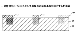
次に、図8に示すように、第1の絶縁体12を埋込んだ導体基板11上で、ナノホールアレイ13を形成する領域以外を覆うようにフォトレジスト23をパターニングする。フォトレジスト23は、感光性樹脂であれば特に限定されず、ドライフィルムレジスト、液状レジストなどを使用することが可能である。また、フォトレジスト23を露光するのに用いる光源は、g線、h線、i線、電子線、及びX線のいずれを照射するものであっても良く、さらに、ポジ型及びネガ型のいずれのフォトレジスト23に対しても用いることができる。
Next, as shown in FIG. 8, a
具体的には、例えばポジ型レジスト(例えば、AZエレクトロニックマテリアルズ社製のAZP−4620)を5000rpmで60秒の条件でスピンコータによりスピンコートした後、110℃で60秒のプリベークを行う。その後、光源にi線を搭載したコンタクトアライナを用いて、ナノホールアレイ13を形成する領域に紫外線照射を行い、2.38%のTMAH溶液にてアルカリ現像を行うことで、ナノホールアレイ13を形成する領域以外を覆うように、ポジ型レジストをパターニングする。
Specifically, for example, a positive resist (for example, AZP-4620 manufactured by AZ Electronic Materials) is spin-coated with a spin coater at 5000 rpm for 60 seconds, and then pre-baked at 110 ° C. for 60 seconds. Thereafter, using a contact aligner equipped with i rays as a light source, the region where the
次に、図9に示すように、導体基板11が露出した箇所にナノホールアレイ13を形成する。ナノホールアレイ13の形成方法は、直径が数nmから数百nmのナノホール13Aが形成できれば特に限定されず、陽極酸化法、集束イオンビーム加工、レーザ加工などを用いることができる。例えば、ナノホールアレイ状に形成したレジストパターンをマスクとして用いて、ドライエッチング加工によりナノホール13Aを形成しても良い。ただし、ナノホール13Aの側壁は、金属酸化物である必要があるため、ナノホール13Aの形成と導体(即ち、ナノホール13Aを形成する導体基板11の側壁)の酸化が同時に進行する陽極酸化法を用いることが好ましい。また、陽極酸化法にてナノホールアレイ13を形成する場合は、電解液にしゅう酸、硫酸、りん酸などの酸性水溶液を用い、導体基板11とカソード電極間に印加する電圧は10V〜80Vの範囲であることが好ましい。なお、この陽極酸化工程にてナノホール13Aが所望のサイズにならない場合は、例えばりん酸水溶液などの酸性溶液に浸漬してナノホール13Aを広げても良い。また、酸化物の特性を改善する目的で、ナノホール13Aの形成後にアニールを行っても良い。
Next, as shown in FIG. 9, the
具体的には、例えば0.5molのしゅう酸水溶液を恒温水槽により10℃に保持し、アルミ基板を恒温水槽内のしゅう酸水溶液に浸漬する。また、白金のカソード電極を用いてアルミ基板とカソード電極間にDC80Vの電圧を印加することで、ナノホールアレイ13を形成する。この時のナノホールアレイ13のサイズを電子顕微鏡により測定したところ、直径が約50nmであることが確認された。
Specifically, for example, a 0.5 mol oxalic acid aqueous solution is held at 10 ° C. by a constant temperature water bath, and the aluminum substrate is immersed in the oxalic acid aqueous solution in the constant temperature water bath. Further, a
次に、図10に示すように、形成されたナノホールアレイ13を覆うように、感ガス材料の感ガス膜13Bを形成する。感ガス膜13Bは、ナノホール13Aを形成する導体基板11の壁面を含めて各センサブロック13−1〜13−4内の導体基板11の第1の面(隣接するナノホール13A間の表面)に形成される。感ガス材料は、検知対象ガスを吸着できれば特に限定されない。また、感ガス膜13Bの形成方法は、感ガス材料をナノホール13Aを形成する壁面に固定化できれば特に限定されず、例えばナノホールアレイ13に感ガス材料を含む溶液を含浸させても良いし、ナノホールアレイ13を感ガス材料の蒸気に暴露させても良い。
Next, as shown in FIG. 10, a gas
具体的には、例えばナノホールアレイ13にSnCl4及びWCl6 の蒸気を暴露することで、感ガス材料を形成する。
Specifically, for example, the gas-sensitive material is formed by exposing the vapor of SnCl 4 and WCl 6 to the
次に、図11に示すように、フォトレジスト23を除去し、第1の絶縁体12上に、対応するセンシングブロック内の感ガス膜13Bの両端と電気的に接続するように、電極14の各対を形成する。
Next, as shown in FIG. 11, the
次に、図12に示すように、導体基板11の下面に第2の絶縁体15を形成し、第2の絶縁体15の下面(即ち、露出している表面)にヒータ16を形成する。
Next, as shown in FIG. 12, the
さらに、ヒータ16に接続するように例えば図3または図4に示す配置で電極17を形成し、必要に応じて抵抗温度センサ50を第2の絶縁体15の表面などに形成することで、図1に示すガスセンサ1を作製することができる。
Further, the
なお、ヒータ16及び電極17の形成するタイミングは、上記のタイミングに限定されず、図5乃至図11と共に説明した工程のいずれかのタイミングで形成しても良い。
Note that the timing of forming the
また、各センシングブロック13−1〜13−4の平面形状及びサイズ、各センシングブロック13−1〜13−4におけるナノホール13Aの直径、深さ及び形状のうち少なくとも1つを、検知対象ガスの種類に応じて制御するようにしても良い。
In addition, at least one of the planar shape and size of each sensing block 13-1 to 13-4 and the diameter, depth, and shape of the
次に、作製したガスセンサの評価結果について説明する。例えば、センシングブロック13−1,13−2にはホルムアルデヒドを検知する感ガス材料の感ガス膜13Bが形成され、センシングブロック13−3,13−4にはトルエンを検知する感ガス材料の感ガス膜13Bが形成されたガスセンサ1を、上記の製造方法で作製した。このように作製したガスセンサ1の電極14をLCRメータに接続し、密閉チャンバに入れた後、窒素ガスで希釈したホルムアルデヒド及びトルエンを用いて検出範囲を測定した。この測定の結果、ホルムアルデヒドは0.1ppm〜200ppm、トルエンは0.5ppm〜100ppmであり、複数種類のガスを安定した感度で検知できることが確認された。また、このガスセンサ1を1ヶ月の間連続して駆動したところ、検出感度が低下しないことが確認された。さらに、ナノホール13Aは、各センシングブロック13−1〜13−4内で規則的に(例えば、一定のピッチ)で設けられているので、作製した複数のガスセンサ1間で、各検知対象ガスに対する感度に個体差が生じにくいことも確認された。
Next, the evaluation result of the produced gas sensor will be described. For example, the sensing blocks 13-1 and 13-2 are formed with a gas-
上記の如く、開示のガスセンサによれば、小型で複数種類の検知対象ガスをリアルタイムで検知可能な環境センサデバイスの一例を形成できる。このため、ガスセンサを、例えば携帯電話、PDA(Personal Digital Assistant)、ノート型PC(Personal Computer)、電子辞書などの小型モバイル電子装置に内蔵させることも可能となる。また、ガスセンサを、有線または無線通信機能を有する電子装置に内蔵することにより、各計測点における大気汚染状況を把握できる。さらに、広域ネットワークを通じてガスセンサから取得したデータを統計化することで、汚染源の特定や広域情報を発信するシステムやサービスなどへの応用も可能である。 As described above, according to the disclosed gas sensor, an example of an environmental sensor device that can detect a plurality of types of detection target gas in real time in a small size can be formed. For this reason, the gas sensor can be incorporated in a small mobile electronic device such as a mobile phone, a PDA (Personal Digital Assistant), a notebook PC (Personal Computer), or an electronic dictionary. Further, by incorporating the gas sensor in an electronic device having a wired or wireless communication function, it is possible to grasp the air pollution status at each measurement point. Furthermore, by statisticalizing the data acquired from the gas sensor through the wide area network, it can be applied to a system or service for identifying a pollution source or transmitting wide area information.
以上の実施例を含む実施形態に関し、更に以下の付記を開示する。
(付記1)
導体基板の第1の面が第1の絶縁体により電気的に絶縁された複数のセンシングブロックに分割されたナノホールアレイと、
前記第1の絶縁体の表面に、前記複数のセンシングブロックの各々に対して設けられた一対の電極と、
前記導体基板の前記第1の面とは反対側の第2の面上に、第2の絶縁体を介して設けられたヒータと、
を備え、
前記複数のセンシングブロックの各々は、前記第1の面に形成された複数のナノホールと、前記複数のナノホールを形成する前記導体基板の壁面を含めて前記第1の面に形成され前記一対の電極と電気的に接続する感ガス膜とを有し、
前記複数のセンシングブロックのうち、少なくとも2つのセンシングブロック間では前記感ガス膜が異なる感ガス材料で形成されていることを特徴とする、ガスセンサ。
(付記2)
前記第1の絶縁体は、前記導体基板の前記第1の面に、前記複数のセンシングブロックを電気的に絶縁するように埋め込まれており、
前記複数のセンシングブロックの各々において、前記感ガス膜は前記第1の絶縁体により囲まれていることを特徴とする、付記1記載のガスセンサ。
(付記3)
前記複数のセンシングブロックの各々は、抵抗変化検出型センサ素子を形成することを特徴とする、付記1または2記載のガスセンサ。
(付記4)
前記電極は、前記複数のセンシングブロックの各々において、前記感ガス膜の外周部の対向する辺の少なくとも一部と接触していることを特徴とする、付記1乃至3のいずれか1項記載のガスセンサ。
(付記5)
前記第1の絶縁体の前記表面に設けられ、前記複数のセンシングブロックにより検知対象ガスのガス濃度を検出するのと並行して、前記複数のセンシングブロックの温度を検出する抵抗温度センサを更に備え、
前記温度に応じて変化する前記感ガス膜の抵抗値をキャンセルするための温度情報を、検出した前記ガス濃度を表す情報が電極の各対から出力されるのと並行して、前記抵抗温度センサから出力することを特徴とする、付記1乃至4のいずれか1項記載のガスセンサ。
(付記6)
前記感ガス材料は、チタン、スズ、アルミ、銅、及びニッケルの中から選ばれた金属を主成分とする酸化物であることを特徴とする、付記1乃至5のいずれか1項記載のガスセンサ。
(付記7)
前記複数のセンシングブロックの各々の平面形状及びサイズ、前記複数のセンシングブロックの各々内における前記ナノホールの直径、深さ及び形状のうち少なくとも1つは、検知対象ガスの種類に応じて選定されていることを特徴とする、付記1乃至6のいずれか1項記載のガスセンサ。
(付記8)
前記ヒータと電気的に接続された一対の電極をさらに備えたことを特徴とする、付記1乃至7のいずれか1項記載のガスセンサ。
(付記9)
前記導体基板の前記第1の面、前記第1の絶縁体の表面、及び前記ナノホールアレイの表面を含む面は、平面形状または略平面形状または曲面形状を有することを特徴とする、付記1乃至8のいずれか1項記載のガスセンサ。
(付記10)
導体基板の第1の面に溝を形成し、
前記溝内に第1の絶縁体を埋め込んで、前記第1の面を前記第1の絶縁体により電気的に絶縁された複数のセンシングブロックに分割し、
前記第1の絶縁体に囲まれた複数の領域内に、前記第1の面に形成された複数のナノホールを形成し、
前記ナノホールを形成する前記導体基板の壁面を含めて前記第1の面に感ガス膜を形成してナノホールアレイを形成し、
前記複数のセンシングブロックの各々に対して前記感ガス膜と接触する一対の電極を形成し、
前記導体基板の前記第1の面とは反対側の第2の面上に、第2の絶縁体を形成し、
前記第2の絶縁体の表面にヒータを形成し、
前記複数のセンシングブロックのうち、少なくとも2つのセンシングブロック間では前記感ガス膜を異なる感ガス材料で形成することを特徴とする、ガスセンサの製造方法。
(付記11)
前記感ガス材料は、チタン、スズ、アルミ、銅、及びニッケルの中から選ばれた金属を主成分とする酸化物であることを特徴とする、付記10記載のガスセンサの製造方法。
(付記12)
前記ナノホールの形成と前記側壁の酸化が同時に進行する陽極酸化法を用い、
前記側壁に金属酸化物を形成することを特徴とする、付記10または11記載のガスセンサの製造方法。
(付記13)
前記複数のセンシングブロックの各々の平面形状及びサイズ、前記複数のセンシングブロックの各々内における前記ナノホールの直径、深さ及び形状のうち少なくとも1つを、検知対象ガスの種類に応じて制御することを特徴とする、付記10乃至12のいずれか1項記載のガスセンサの製造方法。
The following additional notes are further disclosed with respect to the embodiment including the above examples.
(Appendix 1)
A nanohole array divided into a plurality of sensing blocks in which a first surface of a conductor substrate is electrically insulated by a first insulator;
A pair of electrodes provided for each of the plurality of sensing blocks on the surface of the first insulator;
A heater provided on a second surface opposite to the first surface of the conductive substrate via a second insulator;
With
Each of the plurality of sensing blocks is formed on the first surface including the plurality of nanoholes formed on the first surface and the wall surface of the conductive substrate forming the plurality of nanoholes. And a gas sensitive film electrically connected to
The gas sensor, wherein the gas sensitive film is formed of different gas sensitive materials between at least two sensing blocks among the plurality of sensing blocks.
(Appendix 2)
The first insulator is embedded in the first surface of the conductor substrate so as to electrically insulate the plurality of sensing blocks;
The gas sensor according to
(Appendix 3)
The gas sensor according to
(Appendix 4)
4. The appendix according to
(Appendix 5)
A resistance temperature sensor is provided on the surface of the first insulator and further detects a temperature of the plurality of sensing blocks in parallel with detecting the gas concentration of the detection target gas by the plurality of sensing blocks. ,
The temperature sensor for canceling the resistance value of the gas sensitive film that changes according to the temperature, the resistance temperature sensor in parallel with the information indicating the detected gas concentration being output from each pair of electrodes. The gas sensor according to any one of
(Appendix 6)
The gas sensor according to any one of
(Appendix 7)
At least one of the planar shape and size of each of the plurality of sensing blocks and the diameter, depth, and shape of the nanohole in each of the plurality of sensing blocks is selected according to the type of detection target gas. The gas sensor according to any one of
(Appendix 8)
The gas sensor according to any one of
(Appendix 9)
The first surface of the conductive substrate, the surface of the first insulator, and the surface including the surface of the nanohole array have a planar shape, a substantially planar shape, or a curved surface shape. The gas sensor according to any one of 8.
(Appendix 10)
Forming a groove in the first surface of the conductor substrate;
Burying a first insulator in the groove and dividing the first surface into a plurality of sensing blocks electrically insulated by the first insulator;
Forming a plurality of nanoholes formed on the first surface in a plurality of regions surrounded by the first insulator;
Forming a nanohole array by forming a gas sensitive film on the first surface including the wall surface of the conductive substrate forming the nanohole;
Forming a pair of electrodes in contact with the gas-sensitive film for each of the plurality of sensing blocks;
Forming a second insulator on a second surface of the conductor substrate opposite to the first surface;
Forming a heater on the surface of the second insulator;
A gas sensor manufacturing method, wherein the gas sensitive film is formed of different gas sensitive materials between at least two sensing blocks among the plurality of sensing blocks.
(Appendix 11)
11. The method of manufacturing a gas sensor according to appendix 10, wherein the gas sensitive material is an oxide mainly composed of a metal selected from titanium, tin, aluminum, copper, and nickel.
(Appendix 12)
Using an anodic oxidation method in which the formation of the nanoholes and the oxidation of the side walls proceed simultaneously,
12. The method for manufacturing a gas sensor according to
(Appendix 13)
Controlling at least one of the planar shape and size of each of the plurality of sensing blocks and the diameter, depth, and shape of the nanohole in each of the plurality of sensing blocks according to the type of detection target gas. The method of manufacturing a gas sensor according to any one of appendices 10 to 12, which is characterized in that
以上、開示のガスセンサ及びその製造方法を実施例により説明したが、本発明は上記実施例に限定されるものではなく、本発明の範囲内で種々の変形及び改良が可能であることは言うまでもない。 As mentioned above, although the gas sensor of the indication and its manufacturing method were explained by an example, the present invention is not limited to the above-mentioned example, and it cannot be overemphasized that various modification and improvement are possible within the scope of the present invention. .
1 ガスセンサ
11 導体基板
12 第1の絶縁体
13 ナノホールアレイ
13−1〜13−4 センシングブロック
13A ナノホール
13B 感ガス膜
14,17 電極
15 第2の絶縁体
16 ヒータ
50 抵抗温度センサ
DESCRIPTION OF
Claims (5)
前記第1の絶縁体の表面に、前記複数のセンシングブロックの各々に対して設けられた一対の電極と、
前記導体基板の前記第1の面とは反対側の第2の面上に、第2の絶縁体を介して設けられたヒータと、
を備え、
前記複数のセンシングブロックの各々は、前記第1の面に形成された複数のナノホールと、前記複数のナノホールを形成する前記導体基板の壁面を含めて前記第1の面に形成され前記一対の電極と電気的に接続する感ガス膜とを有し、
前記複数のセンシングブロックのうち、少なくとも2つのセンシングブロック間では前記感ガス膜が異なる感ガス材料で形成されていることを特徴とする、ガスセンサ。 A nanohole array divided into a plurality of sensing blocks in which a first surface of a conductor substrate is electrically insulated by a first insulator;
A pair of electrodes provided for each of the plurality of sensing blocks on the surface of the first insulator;
A heater provided on a second surface opposite to the first surface of the conductive substrate via a second insulator;
With
Each of the plurality of sensing blocks is formed on the first surface including the plurality of nanoholes formed on the first surface and the wall surface of the conductive substrate forming the plurality of nanoholes. And a gas sensitive film electrically connected to
The gas sensor, wherein the gas sensitive film is formed of different gas sensitive materials between at least two sensing blocks among the plurality of sensing blocks.
前記複数のセンシングブロックの各々において、前記感ガス膜は前記第1の絶縁体により囲まれていることを特徴とする、請求項1記載のガスセンサ。 The first insulator is embedded in the first surface of the conductor substrate so as to electrically insulate the plurality of sensing blocks;
The gas sensor according to claim 1, wherein in each of the plurality of sensing blocks, the gas sensitive film is surrounded by the first insulator.
前記温度に応じて変化する前記感ガス膜の抵抗値をキャンセルするための温度情報を、検出した前記ガス濃度を表す情報が前記電極の各対から出力されるのと並行して、前記抵抗温度センサから出力することを特徴とする、請求項1乃至3のいずれか1項記載のガスセンサ。 A resistance temperature sensor is provided on the surface of the first insulator and further detects a temperature of the plurality of sensing blocks in parallel with detecting the gas concentration of the detection target gas by the plurality of sensing blocks. ,
The temperature information for canceling the resistance value of the gas-sensitive film, which changes according to the temperature, in parallel with the information indicating the detected gas concentration being output from each pair of the electrodes The gas sensor according to any one of claims 1 to 3, wherein the gas sensor outputs from the sensor.
前記溝内に第1の絶縁体を埋め込んで、前記第1の面を前記第1の絶縁体により電気的に絶縁された複数のセンシングブロックに分割し、
前記第1の絶縁体に囲まれた複数の領域内に、前記第1の面に形成された複数のナノホールを形成し、
前記ナノホールを形成する前記導体基板の壁面を含めて前記第1の面に感ガス膜を形成してナノホールアレイを形成し、
前記複数のセンシングブロックの各々に対して前記感ガス膜と接触する一対の電極を形成し、
前記導体基板の前記第1の面とは反対側の第2の面上に、第2の絶縁体を形成し、
前記第2の絶縁体の表面にヒータを形成し、
前記複数のセンシングブロックのうち、少なくとも2つのセンシングブロック間では前記感ガス膜を異なる感ガス材料で形成することを特徴とする、ガスセンサの製造方法。 Forming a groove in the first surface of the conductor substrate;
Burying a first insulator in the groove and dividing the first surface into a plurality of sensing blocks electrically insulated by the first insulator;
Forming a plurality of nanoholes formed on the first surface in a plurality of regions surrounded by the first insulator;
Forming a nanohole array by forming a gas sensitive film on the first surface including the wall surface of the conductive substrate forming the nanohole;
Forming a pair of electrodes in contact with the gas-sensitive film for each of the plurality of sensing blocks;
Forming a second insulator on a second surface of the conductor substrate opposite to the first surface;
Forming a heater on the surface of the second insulator;
A gas sensor manufacturing method, wherein the gas sensitive film is formed of different gas sensitive materials between at least two sensing blocks among the plurality of sensing blocks.
Priority Applications (1)
| Application Number | Priority Date | Filing Date | Title |
|---|---|---|---|
| JP2016019079A JP2017138191A (en) | 2016-02-03 | 2016-02-03 | Gas sensor and manufacturing method therefor |
Applications Claiming Priority (1)
| Application Number | Priority Date | Filing Date | Title |
|---|---|---|---|
| JP2016019079A JP2017138191A (en) | 2016-02-03 | 2016-02-03 | Gas sensor and manufacturing method therefor |
Publications (1)
| Publication Number | Publication Date |
|---|---|
| JP2017138191A true JP2017138191A (en) | 2017-08-10 |
Family
ID=59565785
Family Applications (1)
| Application Number | Title | Priority Date | Filing Date |
|---|---|---|---|
| JP2016019079A Pending JP2017138191A (en) | 2016-02-03 | 2016-02-03 | Gas sensor and manufacturing method therefor |
Country Status (1)
| Country | Link |
|---|---|
| JP (1) | JP2017138191A (en) |
Cited By (2)
| Publication number | Priority date | Publication date | Assignee | Title |
|---|---|---|---|---|
| CN110779963A (en) * | 2018-07-25 | 2020-02-11 | 意法半导体有限公司 | Selective multi-gas detection by pulse heating in gas sensors |
| CN114836719A (en) * | 2022-05-11 | 2022-08-02 | 东南大学 | Cu-Ni film material for temperature sensing and preparation method thereof |
-
2016
- 2016-02-03 JP JP2016019079A patent/JP2017138191A/en active Pending
Cited By (3)
| Publication number | Priority date | Publication date | Assignee | Title |
|---|---|---|---|---|
| CN110779963A (en) * | 2018-07-25 | 2020-02-11 | 意法半导体有限公司 | Selective multi-gas detection by pulse heating in gas sensors |
| CN114836719A (en) * | 2022-05-11 | 2022-08-02 | 东南大学 | Cu-Ni film material for temperature sensing and preparation method thereof |
| CN114836719B (en) * | 2022-05-11 | 2023-09-15 | 东南大学 | Cu-Ni film material for temperature sensing and preparation method thereof |
Similar Documents
| Publication | Publication Date | Title |
|---|---|---|
| EP2815425B1 (en) | Noise shielding techniques for ultra low current measurements in biochemical applications | |
| US8736000B1 (en) | Capacitive chemical sensor | |
| Mu et al. | A robust flexible electrochemical gas sensor using room temperature ionic liquid | |
| EP2762866B1 (en) | CMOS gas sensor and method for manufacturing the same | |
| Mahboob et al. | A sensitive and highly linear capacitive thin film sensor for trace moisture measurement in gases | |
| BR112015008202B1 (en) | device for the quantitative detection of a substance in a fluid sample and use of a device | |
| JP2012047536A (en) | Current detection device | |
| KR20130033939A (en) | Fabrication method for gas sensor and temperature sensor based on suspended carbon nanowires | |
| CN105954333A (en) | Gold nanobelt three-electrode sensor used for monitoring heavy metal and preparation method thereof | |
| JP2017138191A (en) | Gas sensor and manufacturing method therefor | |
| CN110672666A (en) | Electronic nose device and preparation method thereof | |
| CN118032873A (en) | Hydrogen sulfide gas sensor and preparation process thereof | |
| Han et al. | Modulation and Modeling of Three‐Dimensional Nanowire Assemblies Targeting Gas Sensors with High Response and Reliability | |
| KR102125278B1 (en) | GAS SENSOR and Method for Manufacturing GAS SENSOR | |
| KR20140118020A (en) | Hydrogen gas sensor and method for manufacturing the same | |
| Truong et al. | A Partially Etched Structure of Light‐Addressable Potentiometric Sensor for High‐Spatial‐Resolution and High‐Speed Chemical Imaging | |
| JP6439577B2 (en) | Gas sensor device, gas sensor device and manufacturing method thereof, information processing system | |
| KR100845717B1 (en) | Biomaker sensor and module using micro bridge mass sensor | |
| US20170067844A1 (en) | Electrochemical detector | |
| CN107132497A (en) | Substrate for Non-Destructive Testing semiconductive thin film Hall effect and preparation method thereof | |
| Mazerie et al. | A General Approach Based on Sampled‐Current Voltammetry for Minimizing Electrode Fouling in Electroanalytical Detection | |
| US20130187670A1 (en) | Capacitive sensors and methods of fabrication | |
| JP5681965B2 (en) | Detection element and detection device using the same | |
| KR20130134538A (en) | Ultra-sensitive graphene sensor for controlling efficiency, and manufacturing method thereof | |
| Lee et al. | Thermally/mechanically robust anodic aluminum oxide (AAO) microheater platform for low power chemoresistive gas sensor |