JP2017133894A - Scintillator array and x-ray detector and x-ray inspection device using the same - Google Patents
Scintillator array and x-ray detector and x-ray inspection device using the same Download PDFInfo
- Publication number
- JP2017133894A JP2017133894A JP2016012803A JP2016012803A JP2017133894A JP 2017133894 A JP2017133894 A JP 2017133894A JP 2016012803 A JP2016012803 A JP 2016012803A JP 2016012803 A JP2016012803 A JP 2016012803A JP 2017133894 A JP2017133894 A JP 2017133894A
- Authority
- JP
- Japan
- Prior art keywords
- scintillator array
- scintillator
- ray
- dielectric layers
- refractive index
- Prior art date
- Legal status (The legal status is an assumption and is not a legal conclusion. Google has not performed a legal analysis and makes no representation as to the accuracy of the status listed.)
- Pending
Links
- 238000007689 inspection Methods 0.000 title claims abstract description 25
- 239000000463 material Substances 0.000 claims abstract description 20
- 239000003989 dielectric material Substances 0.000 claims description 32
- 239000000919 ceramic Substances 0.000 claims description 9
- XQPRBTXUXXVTKB-UHFFFAOYSA-M caesium iodide Chemical compound [I-].[Cs+] XQPRBTXUXXVTKB-UHFFFAOYSA-M 0.000 claims description 8
- 238000000034 method Methods 0.000 claims description 8
- 238000004544 sputter deposition Methods 0.000 claims description 7
- 229910052777 Praseodymium Inorganic materials 0.000 claims description 6
- 238000007740 vapor deposition Methods 0.000 claims description 6
- 229910004298 SiO 2 Inorganic materials 0.000 claims description 4
- 229910010413 TiO 2 Inorganic materials 0.000 claims description 4
- 229910052793 cadmium Inorganic materials 0.000 claims description 4
- BDOSMKKIYDKNTQ-UHFFFAOYSA-N cadmium atom Chemical compound [Cd] BDOSMKKIYDKNTQ-UHFFFAOYSA-N 0.000 claims description 4
- 238000005229 chemical vapour deposition Methods 0.000 claims description 4
- 239000013078 crystal Substances 0.000 claims description 4
- 239000011224 oxide ceramic Substances 0.000 claims description 4
- 238000005240 physical vapour deposition Methods 0.000 claims description 4
- -1 praseodymium activated gadolinium oxysulfide Chemical class 0.000 claims description 4
- 229910001404 rare earth metal oxide Inorganic materials 0.000 claims description 4
- FVAUCKIRQBBSSJ-UHFFFAOYSA-M sodium iodide Chemical compound [Na+].[I-] FVAUCKIRQBBSSJ-UHFFFAOYSA-M 0.000 claims description 4
- PBYZMCDFOULPGH-UHFFFAOYSA-N tungstate Chemical compound [O-][W]([O-])(=O)=O PBYZMCDFOULPGH-UHFFFAOYSA-N 0.000 claims description 4
- 229910052693 Europium Inorganic materials 0.000 claims description 3
- 229910052797 bismuth Inorganic materials 0.000 claims description 3
- 239000002223 garnet Substances 0.000 claims description 3
- 238000001704 evaporation Methods 0.000 claims description 2
- 229910044991 metal oxide Inorganic materials 0.000 claims 1
- 150000004706 metal oxides Chemical class 0.000 claims 1
- 238000001514 detection method Methods 0.000 description 15
- 238000006243 chemical reaction Methods 0.000 description 10
- 230000000052 comparative effect Effects 0.000 description 8
- 239000012190 activator Substances 0.000 description 7
- 229910052761 rare earth metal Inorganic materials 0.000 description 7
- 229920005989 resin Polymers 0.000 description 7
- 239000011347 resin Substances 0.000 description 7
- UAHZTKVCYHJBJQ-UHFFFAOYSA-N [P].S=O Chemical compound [P].S=O UAHZTKVCYHJBJQ-UHFFFAOYSA-N 0.000 description 5
- 239000000843 powder Substances 0.000 description 5
- 150000002910 rare earth metals Chemical class 0.000 description 5
- 230000035945 sensitivity Effects 0.000 description 5
- 238000010521 absorption reaction Methods 0.000 description 4
- 238000010586 diagram Methods 0.000 description 4
- 238000003384 imaging method Methods 0.000 description 4
- 239000002245 particle Substances 0.000 description 4
- 239000010936 titanium Substances 0.000 description 4
- OAICVXFJPJFONN-UHFFFAOYSA-N Phosphorus Chemical compound [P] OAICVXFJPJFONN-UHFFFAOYSA-N 0.000 description 3
- 239000012535 impurity Substances 0.000 description 3
- PUDIUYLPXJFUGB-UHFFFAOYSA-N praseodymium atom Chemical compound [Pr] PUDIUYLPXJFUGB-UHFFFAOYSA-N 0.000 description 3
- XKRFYHLGVUSROY-UHFFFAOYSA-N Argon Chemical compound [Ar] XKRFYHLGVUSROY-UHFFFAOYSA-N 0.000 description 2
- GWEVSGVZZGPLCZ-UHFFFAOYSA-N Titan oxide Chemical compound O=[Ti]=O GWEVSGVZZGPLCZ-UHFFFAOYSA-N 0.000 description 2
- 239000000853 adhesive Substances 0.000 description 2
- 230000001070 adhesive effect Effects 0.000 description 2
- 238000003491 array Methods 0.000 description 2
- 238000003745 diagnosis Methods 0.000 description 2
- 230000000694 effects Effects 0.000 description 2
- 239000011159 matrix material Substances 0.000 description 2
- 238000005259 measurement Methods 0.000 description 2
- 230000003287 optical effect Effects 0.000 description 2
- 238000012545 processing Methods 0.000 description 2
- 238000005245 sintering Methods 0.000 description 2
- 239000007787 solid Substances 0.000 description 2
- 238000003325 tomography Methods 0.000 description 2
- 229910052684 Cerium Inorganic materials 0.000 description 1
- KRHYYFGTRYWZRS-UHFFFAOYSA-M Fluoride anion Chemical compound [F-] KRHYYFGTRYWZRS-UHFFFAOYSA-M 0.000 description 1
- 229910052688 Gadolinium Inorganic materials 0.000 description 1
- XUIMIQQOPSSXEZ-UHFFFAOYSA-N Silicon Chemical compound [Si] XUIMIQQOPSSXEZ-UHFFFAOYSA-N 0.000 description 1
- MCVAAHQLXUXWLC-UHFFFAOYSA-N [O-2].[O-2].[S-2].[Gd+3].[Gd+3] Chemical compound [O-2].[O-2].[S-2].[Gd+3].[Gd+3] MCVAAHQLXUXWLC-UHFFFAOYSA-N 0.000 description 1
- 239000004840 adhesive resin Substances 0.000 description 1
- 229920006223 adhesive resin Polymers 0.000 description 1
- 229910052786 argon Inorganic materials 0.000 description 1
- 239000002775 capsule Substances 0.000 description 1
- 150000001875 compounds Chemical class 0.000 description 1
- 230000001066 destructive effect Effects 0.000 description 1
- 230000006866 deterioration Effects 0.000 description 1
- 238000011161 development Methods 0.000 description 1
- 150000002222 fluorine compounds Chemical class 0.000 description 1
- UIWYJDYFSGRHKR-UHFFFAOYSA-N gadolinium atom Chemical compound [Gd] UIWYJDYFSGRHKR-UHFFFAOYSA-N 0.000 description 1
- 239000007789 gas Substances 0.000 description 1
- 238000004519 manufacturing process Methods 0.000 description 1
- BPUBBGLMJRNUCC-UHFFFAOYSA-N oxygen(2-);tantalum(5+) Chemical compound [O-2].[O-2].[O-2].[O-2].[O-2].[Ta+5].[Ta+5] BPUBBGLMJRNUCC-UHFFFAOYSA-N 0.000 description 1
- 125000002467 phosphate group Chemical group [H]OP(=O)(O[H])O[*] 0.000 description 1
- 229910052698 phosphorus Inorganic materials 0.000 description 1
- 229920000642 polymer Polymers 0.000 description 1
- 230000005855 radiation Effects 0.000 description 1
- 238000002310 reflectometry Methods 0.000 description 1
- 238000011160 research Methods 0.000 description 1
- 229910052710 silicon Inorganic materials 0.000 description 1
- 239000010703 silicon Substances 0.000 description 1
- 238000006467 substitution reaction Methods 0.000 description 1
- 150000004763 sulfides Chemical class 0.000 description 1
- XTQHKBHJIVJGKJ-UHFFFAOYSA-N sulfur monoxide Chemical compound S=O XTQHKBHJIVJGKJ-UHFFFAOYSA-N 0.000 description 1
- OGIDPMRJRNCKJF-UHFFFAOYSA-N titanium oxide Inorganic materials [Ti]=O OGIDPMRJRNCKJF-UHFFFAOYSA-N 0.000 description 1
- 229910052726 zirconium Inorganic materials 0.000 description 1
Images

Abstract
Description
本発明の実施形態は、X線などの放射線を可視光線などに変換する発光素子であるシンチレータアレイおよびそのシンチレータアレイを具備したX線検出器並びにX線検査装置に関する。 Embodiments described herein relate generally to a scintillator array that is a light-emitting element that converts radiation such as X-rays into visible light, an X-ray detector including the scintillator array, and an X-ray inspection apparatus.
医療診断や工業用非破壊検査などの分野においては、X線断層写真撮影装置(以下、X線CT装置と記す)などのX線検査装置を用いた検査が行なわれている。X線CT装置は、扇状のファンビームX線を照射するX線管(X線源)と、多数のX線検出素子を併設したX線検出器とを、被検査体の断層面を中央として対向配置して構成されている。このようなX線CT装置においてはX線検出器に向けてX線管からファンビームX線を照射し、1回照射を行う毎に断層面に対して例えば角度を1度ずつ変えてゆくことによってX線吸収データを収集した後、このデータをコンピュータで解析することによって断層面の個々の位置でのX線吸収率を算出し、その吸収率に応じた画像を構成するものである。
X線CT装置のX線検出器では、X線の刺激により可視光線等を放射するシンチレータアレイとフォトダイオードを組み合わせた検出器の開発が進められている。このシンチレータアレイを用いた検出器では、検出素子を小型化し、チャンネル数を増やすことが容易であることから、高解像度のX線CT装置を得ることが可能となる。
In fields such as medical diagnosis and industrial non-destructive inspection, inspection using an X-ray inspection apparatus such as an X-ray tomography apparatus (hereinafter referred to as X-ray CT apparatus) is performed. The X-ray CT system uses an X-ray tube (X-ray source) that irradiates a fan-shaped fan beam X-ray and an X-ray detector with a large number of X-ray detection elements, with the tomographic plane of the object to be inspected at the center. It is configured to face each other. In such an X-ray CT apparatus, a fan beam X-ray is irradiated from an X-ray tube toward an X-ray detector, and the angle is changed, for example, by 1 degree with respect to the tomographic plane each time irradiation is performed. After the X-ray absorption data is collected by the above, the data is analyzed by a computer to calculate the X-ray absorption rate at each position on the tomographic plane, and an image corresponding to the absorption rate is constructed.
As for the X-ray detector of the X-ray CT apparatus, the development of a detector that combines a scintillator array that emits visible light and the like by a stimulus of X-rays and a photodiode is underway. In the detector using this scintillator array, it is possible to obtain a high-resolution X-ray CT apparatus because it is easy to downsize the detection element and increase the number of channels.
X線CT装置などのX線検査装置は、医療用または工業用など様々な分野に用いられている。例えば、特開2012−187137号公報(特許文献1)には、検出素子(フォトダイオードなど)を縦横に2次元的に並べてシンチレータアレイを搭載したマルチスライスX線CT装置が開示されている。マルチスライス型とすることにより、輪切り画像を重ねることができ、CT画像を立体的に示すことができる。X線検査装置に搭載されるX線検出器は、検出素子を縦横に複数列並べており、検出素子1個ずつにシンチレータセグメントを備えている。シンチレータセグメントに入射したX線が可視光に変換され、その可視光を検出素子で電気信号に変換して画像としている。 X-ray inspection apparatuses such as X-ray CT apparatuses are used in various fields such as medical use and industrial use. For example, Japanese Patent Laying-Open No. 2012-187137 (Patent Document 1) discloses a multi-slice X-ray CT apparatus in which detection elements (photodiodes and the like) are two-dimensionally arranged in a row and a scintillator array. By adopting the multi-slice type, it is possible to overlap the slice images and to show the CT image three-dimensionally. An X-ray detector mounted on an X-ray inspection apparatus has a plurality of detection elements arranged in rows and columns, and includes a scintillator segment for each detection element. X-rays incident on the scintillator segment are converted into visible light, and the visible light is converted into an electrical signal by a detection element to form an image.
従来、X線検出器に用いられるシンチレータアレイは、発光素子であるシンチレータ材料として、例えばタングステン酸カドミウム(CdWO4)、ヨウ化ナトリウム(NaI)、ヨウ化セシウム(CsI)等の単結晶体、特開昭59−27283号公報(特許文献2)に示される立方晶系希土類酸化物セラミックス、特開昭58−204088号公報(特許文献3)に示されるガドリニウム酸硫化物:プラセオジウム(Gd2O2S:Pr)セラミックス、NaGdS2等の固体とこれら固体からなるシンチレータセグメントで発光した光を集光し高感度化することと隣接する発光素子への光漏れ(クロストーク)を低減し低ノイズ化することを目的に反射層、例えば酸化チタン(ルチル型TiO2)粉末を接着剤でかためたもの(特許第3104696号公報(特許文献4))、五酸化タンタル(Ta2O5)粉末を含む接着剤でかためたもの(特許第3715164号公報(特許文献5))や白色ポリマーシートを接着したもの(特許第2930823号公報(特許文献6))などとで構成されている。
Conventionally, scintillator arrays used for X-ray detectors are, for example, single crystal materials such as cadmium tungstate (CdWO 4 ), sodium iodide (NaI), and cesium iodide (CsI) as scintillator materials that are light emitting elements. Cubic rare earth oxide ceramics disclosed in Japanese Utility Model Laid-Open No. 59-27283 (Patent Document 2), gadolinium oxysulfide disclosed in Japanese Patent Application Laid-Open No. 58-204088 (Patent Document 3): praseodymium (Gd 2 O 2 S: Pr) Condensing light emitted from solids such as ceramics and NaGdS2 and scintillator segments made of these solids to increase sensitivity and reducing light leakage (crosstalk) to adjacent light emitting elements to reduce noise reflective layer for the purpose of, for example, titanium oxide (rutile type TiO 2) that the powder solidified with an adhesive (Japanese Patent The 3104696 (Patent Document 4)), five
近年は、前記のX線CT装置の高解像度化に伴い、X線検出器の検出素子の面積を小型化しており、これに伴いシンチレータセグメントのサイズも小さくなっている。すなわち1発光素子に相当するシンチレータセグメントの面積を小型化する必要がある。面積を小型化した発光素子で、これまでの面積の場合と同等以上の検出能力を得るためには、より高感度なシンチレータセグメントが必要となる。一方で、シンチレータセグメントの発光効率を高くすると共にシンチレータセグメントで発光した光の集光効率をあげることが必要である。 In recent years, the area of the detection element of the X-ray detector has been reduced with the increase in the resolution of the X-ray CT apparatus, and the size of the scintillator segment has also been reduced accordingly. That is, it is necessary to reduce the area of the scintillator segment corresponding to one light emitting element. In order to obtain a detection capability equal to or greater than that of the conventional area with a light-emitting element having a reduced area, a more sensitive scintillator segment is required. On the other hand, it is necessary to increase the light emission efficiency of the scintillator segment and increase the light collection efficiency of the light emitted from the scintillator segment.
前記のような従来のシンチレータアレイの構成では、光の集光効率を上げるためには前記の反射層を厚くする必要がある。しかしながら、シンチレータアレイの面積は一定としなくてはならないため、前記のように反射層を厚くするとシンチレータセグメントの開口率が小さくなってしまい、高感度なシンチレータアレイが得られない。さらに、隣接する発光素子への光漏れ(クロストーク)を低減するためにも、前記のような従来の反射層の構成では同様に反射層を厚くする必要があり、前記と同様にシンチレータセグメントの開口率が小さくなってしまい、高感度なシンチレータアレイが得られずX線CT装置の高解像度化の妨げとなっている。このように、反射層をシンチレータセグメントに接着する方法では、X線検出器の1素子あたりを小面積化して、かつ光漏れなどのノイズ低減を行なうことが困難であるという問題を有していた。 In the configuration of the conventional scintillator array as described above, it is necessary to increase the thickness of the reflective layer in order to increase the light collection efficiency. However, since the area of the scintillator array must be constant, if the reflective layer is made thick as described above, the aperture ratio of the scintillator segment becomes small, and a highly sensitive scintillator array cannot be obtained. Further, in order to reduce light leakage (crosstalk) to adjacent light emitting elements, it is necessary to increase the thickness of the reflective layer in the conventional reflective layer structure as described above. The aperture ratio becomes small, and a highly sensitive scintillator array cannot be obtained, which hinders high resolution of the X-ray CT apparatus. As described above, the method of adhering the reflective layer to the scintillator segment has a problem that it is difficult to reduce the area per element of the X-ray detector and reduce noise such as light leakage. .
本発明の実施形態は、このような従来技術の課題に対処するためになされたもので、高解像度化のためにシンチレータセグメントの面積を小型化しても集光効率が高く、光漏れによるノイズが少ないシンチレータアレイを提供すること、および、それを用いたX線検出器およびX線検査装置を提供することを目的としている。 The embodiment of the present invention is made to cope with such problems of the prior art. Even when the area of the scintillator segment is reduced for high resolution, the light collection efficiency is high, and noise due to light leakage is generated. An object of the present invention is to provide a small scintillator array and to provide an X-ray detector and an X-ray inspection apparatus using the same.
本発明の実施形態は、発光素子であるシンチレータ材料の焼結体(インゴット)から加工した複数のシンチレータセグメント間に反射層を介して一体化したシンチレータアレイであり、前記シンチレータセグメント間の反射層として屈折率の差が0.4以上異なる少なくとも2種類の誘電体層を交互に積層した層を複数層有することを特徴とするシンチレータアレイである。前記シンチレータアレイにおいて、前記の屈折率が異なる少なくとも2種類の誘電体層を蒸着法で交互に積層した層を複数層作製したシンチレータアレイである。 An embodiment of the present invention is a scintillator array integrated through a reflective layer between a plurality of scintillator segments processed from a sintered body (ingot) of a scintillator material that is a light emitting element, and as the reflective layer between the scintillator segments A scintillator array comprising a plurality of layers in which at least two types of dielectric layers having different refractive index differences of 0.4 or more are alternately laminated. The scintillator array is a scintillator array in which a plurality of layers in which at least two types of dielectric layers having different refractive indexes are alternately stacked by a vapor deposition method are produced.
前記シンチレータアレイは、シンチレータ材料として、タングステン酸カドミウム(CdWO4)、ヨウ化ナトリウム(NaI)、ヨウ化セシウム(CsI)の単結晶体、立方晶系希土類酸化物セラミックス、プラセオジウム賦活ガドリニウム酸硫化物(Gd2O2S:Pr)セラミックス、ガーネット、NaGdS2:(BiまたはEu)の何れか1種の材料で構成されている。前記シンチレータアレイにおいて、2種類の誘電体層の1種類の誘電体材料はTa2O5、Ti2O3、Ti2O、TiO2、Nb2O5のいずれか1種の材料であり、別の1種類の誘電体材料はMgO、SiO、SiO2いずれか1種の材料である。 The scintillator array includes cadmium tungstate (CdWO 4 ), sodium iodide (NaI), cesium iodide (CsI) single crystals, cubic rare earth oxide ceramics, praseodymium activated gadolinium oxysulfide (as a scintillator material). Gd 2 O 2 S: Pr) ceramics, garnet, or NaGdS 2 : (Bi or Eu). In the scintillator array, one type of dielectric material of the two types of dielectric layers is one of Ta 2 O 5 , Ti 2 O 3 , Ti 2 O, TiO 2 , and Nb 2 O 5 , another one of the dielectric material MgO, SiO, is any one material SiO 2.
本発明者らは、前記の課題を達成するために、(1)シンチレータセグメントと受光素子のサイズが小さくなっていること、(2)シンチレータセグメントの界面には反射層の接着のために透明な樹脂が形成されていることからシンチレータ界面から放出される光は反射層内の反射粒子である白色粉末に到達する前に透明な接着樹脂層を通って受光素子がないエリアに光が到達する、との仮説を立て鋭意研究調査を進めた。その結果、シンチレータセグメント界面に反射率が高い反射層、つまり屈折率差が大きい、少なくとも2種類の誘電体層を蒸着法で直接形成することができることを見出した。
本発明の実施形態であるシンチレータアレイは、発光素子に直接、屈折率が異なる少なくとも2種類の誘電体層を有することを特徴としている。受光素子のX線検出器の素子間隔にあわせてスパッタ法などの蒸着法で作製した誘電体層を具備する反射層間に従来の白色粉末の反射粒子を有する反射層、もしくは遮光層が介在してもかまわない。
また、本発明の実施形態であるX線検出器は、X線により発光する蛍光発生手段と、前記蛍光発生手段からの光を受けて、前記発光出力を電気的出力に変換する光検出手段とを具備するX線検出器であり、前記蛍光発生手段として、前記のシンチレータアレイを用いたことを特徴としている。本発明の実施形態のX線CT装置は、前記のX線検出器を具備することを特徴としている。
In order to achieve the above-mentioned problems, the present inventors have (1) that the size of the scintillator segment and the light receiving element is reduced, and (2) the interface between the scintillator segment is transparent for adhesion of the reflective layer. Since the resin is formed, the light emitted from the scintillator interface reaches the area where there is no light receiving element through the transparent adhesive resin layer before reaching the white powder which is the reflective particle in the reflective layer. Based on this hypothesis, the research was advanced. As a result, it has been found that a reflective layer having a high reflectance at the interface of the scintillator segment, that is, at least two kinds of dielectric layers having a large difference in refractive index can be directly formed by an evaporation method.
The scintillator array according to an embodiment of the present invention is characterized in that the light emitting element has at least two types of dielectric layers having different refractive indexes. A conventional reflective layer having reflective particles of white powder or a light-shielding layer is interposed between the reflective layers having a dielectric layer produced by a vapor deposition method such as sputtering in accordance with the element spacing of the X-ray detector of the light-receiving element. It doesn't matter.
An X-ray detector according to an embodiment of the present invention includes a fluorescence generation unit that emits light by X-rays, and a light detection unit that receives light from the fluorescence generation unit and converts the emission output into an electrical output. The scintillator array is used as the fluorescence generating means. An X-ray CT apparatus according to an embodiment of the present invention includes the X-ray detector described above.
本発明の実施形態では、シンチレータセグメントに、高屈折率誘電体材料と低屈折率誘電体材料の屈折率差が大きい、少なくとも2種類の誘電体材料から構成される誘電体層をスパッタ法でサブミクロン〜数ミクロンの膜厚で均一に直接形成することができるため、感度バラツキが小さい。高屈折率誘電体材料と低屈折率誘電体材料の屈折率差は0.4以上であることが望ましい。また、より反射率を高めるために高屈折率誘電体材料と低屈折率誘電材料を多層化した膜でも構わない。前記2種類の誘電体材料の屈折率差が0.4未満では、反射率を大きくすることが困難である。 In an embodiment of the present invention, a dielectric layer composed of at least two types of dielectric materials having a large refractive index difference between a high refractive index dielectric material and a low refractive index dielectric material is applied to the scintillator segment by sputtering. Since it can be formed directly and uniformly with a film thickness of micron to several microns, there is little variation in sensitivity. The difference in refractive index between the high refractive index dielectric material and the low refractive index dielectric material is preferably 0.4 or more. In order to further increase the reflectance, a film in which a high refractive index dielectric material and a low refractive index dielectric material are multilayered may be used. If the refractive index difference between the two types of dielectric materials is less than 0.4, it is difficult to increase the reflectance.
前記の高屈折率誘電材料としては、屈折率(n)が2.0以上の材料が望ましく、より最適な屈折率は2.2以上であり、材料としては、Ta2O5 (n=2.20)、Ti2O3 (n=2.33)、Ti2O(n=2.35)、TiO2 (n=2.37)、Nb2O5 (n=2.37)などが望ましい。高屈折率誘電体材料の屈折率が2.2未満では、低屈折率誘電体材料との屈折率の差が0.4以上とすることが困難であり、反射率を大きくすることが困難である。
前記の低屈折率誘電体材料としては、屈折率が2.0未満の材料が望ましく、より最適な屈折率は1.8以下であり、材料としては、MgO(n=1.74)、SiO(n=1.7)、SiO2 (n=1.47)などが望ましい。低屈折率誘電体材料の屈折率が2.0以上では、高屈折率誘電材料との屈折率の差が0.4以上とすることが困難であり、反射率を大きくすることが困難である。
前記の各誘電体材料の化合物としては、酸化物以外のフッ化物および硫化物でも構わないが、安定に蒸着できる酸化物が望ましい。
As the high refractive index dielectric material, a material having a refractive index (n) of 2.0 or more is desirable, and a more optimal refractive index is 2.2 or more. As a material, Ta 2 O 5 (n = 2) 20), Ti 2 O 3 (n = 2.33), Ti 2 O (n = 2.35), TiO 2 (n = 2.37), Nb 2 O 5 (n = 2.37), etc. desirable. If the refractive index of the high refractive index dielectric material is less than 2.2, it is difficult to make the difference in refractive index from the low refractive index dielectric material 0.4 or more, and it is difficult to increase the reflectance. is there.
As the low refractive index dielectric material, a material having a refractive index of less than 2.0 is desirable, and a more optimal refractive index is 1.8 or less. Examples of the material include MgO (n = 1.74), SiO 2 (n = 1.7), SiO 2 (n = 1.47), etc. are desirable. When the refractive index of the low refractive index dielectric material is 2.0 or more, it is difficult to make the difference in refractive index from the high refractive index dielectric material 0.4 or more, and it is difficult to increase the reflectance. .
As the compound of each dielectric material, fluorides and sulfides other than oxides may be used, but oxides that can be stably deposited are desirable.
前記の屈折率が異なる少なくとも2種類の誘電体材料層は蒸着法で作製する。蒸着法は、PVD(物理蒸着法)、CVD(化学蒸着法)のいずれか1種で作製する。前記蒸着法としては、スパッタ法で作製することが好ましい。スパッタ法であれば、蒸着膜の厚さを均一で精度よくコントロールして成膜することが可能である。 The at least two types of dielectric material layers having different refractive indexes are produced by vapor deposition. The vapor deposition method is produced by any one of PVD (physical vapor deposition method) and CVD (chemical vapor deposition method). The vapor deposition method is preferably produced by sputtering. If it is a sputtering method, it is possible to form a film by controlling the thickness of the deposited film uniformly and accurately.
本発明を実施するための形態のシンチレータアレイを構成するシンチレータセグメントのシンチレータ材料は、タングステン酸カドミウム(CdWO4)、ヨウ化ナトリウム(NaI)、ヨウ化セシウム(CsI)の単結晶体、立方晶系希土類酸化物セラミックス、プラセオジウム賦活ガドリニウム酸硫化物(Gd2O2S:Pr)セラミックス、ガーネット、NaGdS2:(BiまたはEu)の何れか1種で構成される。 The scintillator material of the scintillator segment constituting the scintillator array of the embodiment for carrying out the present invention is composed of a cadmium tungstate (CdWO 4 ), sodium iodide (NaI), cesium iodide (CsI) single crystal, cubic system Rare earth oxide ceramics, praseodymium activated gadolinium oxysulfide (Gd 2 O 2 S: Pr) ceramics, garnet, NaGdS 2 : (Bi or Eu) are used.
本発明を実施するための形態のシンチレータアレイにおいては、特に、付活剤としてプラセオジム(Pr)を含有する希土類酸硫化物系蛍光体セラミックス(シンチレータ材料)のガドリニウム(Gd)酸硫化物である焼結体からなるものが好ましい。GdはX線吸収係数が大きく、シンチレータアレイの光出力の向上に寄与する。なお、Gdの一部は他の希土類元素で置換してもよい。この際、他の希土類元素による置換量は10mol%以下とすることが好ましい。 In the scintillator array according to the embodiment for carrying out the present invention, in particular, a rare earth oxysulfide phosphor ceramic (scintillator material) gadolinium (Gd) oxysulfide containing praseodymium (Pr) as an activator is sintered. What consists of a combination is preferable. Gd has a large X-ray absorption coefficient and contributes to an improvement in the light output of the scintillator array. A part of Gd may be replaced with other rare earth elements. At this time, the amount of substitution with other rare earth elements is preferably 10 mol% or less.
本発明を実施するための形態においては、希土類酸硫化物系蛍光体セラミックス(シンチレータ材料)の光出力を増大させる付活剤としてプラセオジム(Pr)を使用している。Prは他の付活剤に比べてアフターグローの低減などを図ることができる。従って、付活剤としてPrを含有する希土類酸硫化物系蛍光体セラミックス(シンチレータ材料)は、X線検出器の蛍光発生手段として有効である。 In the embodiment for carrying out the present invention, praseodymium (Pr) is used as an activator for increasing the light output of the rare earth oxysulfide phosphor ceramic (scintillator material). Pr can reduce afterglow compared to other activators. Therefore, the rare earth oxysulfide phosphor ceramic (scintillator material) containing Pr as an activator is effective as a fluorescence generating means of the X-ray detector.
Prの含有量は、蛍光体母体(例えばGd2O2S)に対して0.001〜10mol%の範囲とすることが好ましい。Prの含有量が10mol%を超えると、逆に光出力の低下を招くことになる。一方、Prの含有量が0.001mol%未満では、主付活剤としての効果を十分に得ることができない。より好ましいPrの含有量は0.01〜1mol%の範囲である。 The content of Pr is preferably in the range of 0.001 to 10 mol% with respect to the phosphor matrix (for example, Gd 2 O 2 S). If the Pr content exceeds 10 mol%, the light output is reduced. On the other hand, if the Pr content is less than 0.001 mol%, the effect as the main activator cannot be sufficiently obtained. A more preferable Pr content is in the range of 0.01 to 1 mol%.
本発明を実施するための形態においては、主付活剤としてのPrに加えて、希土類酸硫化物系蛍光体セラミックス(シンチレータ材料)に対してCe、ZrおよびPから選ばれる少なくとも1種を共付活剤として微量含有させてもよい。これら各元素は曝射劣化の抑制、アフターグローの抑制などに対して効果を示す。これら共付活剤の含有量は総量として、蛍光体母体に対して0.00001〜0.1mol%の範囲とすることが好ましい。 In the embodiment for carrying out the present invention, in addition to Pr as the main activator, at least one selected from Ce, Zr and P is co-used with the rare earth oxysulfide phosphor ceramic (scintillator material). A small amount may be contained as an activator. Each of these elements has an effect on suppressing exposure deterioration and afterglow. The total content of these coactivators is preferably in the range of 0.00001 to 0.1 mol% with respect to the phosphor matrix.
さらに、本発明を実施するための形態のシンチレータアレイを構成するシンチレータセグメントを形成するシンチレータ材料の焼結体は、高純度の希土類酸硫化物系蛍光体セラミックス(シンチレータ材料)からなることが好ましい。不純物はシンチレータの感度の低下要因となるため、できるだけ不純物量は低減することが好ましい。特に、燐酸根(PO4)は感度の低下原因となるため、その含有量は150ppm以下とすることが好ましい。なお、特公平5-16756号公報に記載されているように、フッ化物などを焼結助剤として使用して高密度化を図った場合には、前述したように焼結助剤が不純物として残留するため、感度の低下をもたらすことになる。 Furthermore, it is preferable that the sintered body of the scintillator material forming the scintillator segment constituting the scintillator array of the embodiment for carrying out the present invention is made of a high-purity rare earth oxysulfide phosphor ceramic (scintillator material). Since impurities cause a decrease in scintillator sensitivity, it is preferable to reduce the amount of impurities as much as possible. In particular, since phosphate groups (PO 4 ) cause a decrease in sensitivity, the content is preferably 150 ppm or less. In addition, as described in Japanese Patent Publication No. 5-16756, when using a fluoride or the like as a sintering aid to increase the density, the sintering aid is used as an impurity as described above. Since it remains, the sensitivity is lowered.
本発明を実施するための形態のX線検出器は、前記のシンチレータアレイを具備し、入射したX線に応じて前記シンチレータアレイを発光させる蛍光発生手段と、前記蛍光発生手段からの光を受け、前記光の出力を電気的出力に変換する光検出手段(光電変換手段)とを具備することを特徴とするX線検出器である。 An X-ray detector according to an embodiment for carrying out the present invention includes the scintillator array, and generates fluorescence from the scintillator array according to incident X-rays, and receives light from the fluorescence generation means. An X-ray detector comprising: a light detection means (photoelectric conversion means) for converting the light output into an electrical output.
前記蛍光発生手段は、前記シンチレータ材料の焼結体をスライスまたは溝きり加工して作製した前記のシンチレータセグメントを縦横方向に反射層を介して複数集積して構成した前記のシンチレータアレイを有することを特徴とするX線検出器である。 The fluorescence generating means includes the scintillator array configured by stacking a plurality of the scintillator segments produced by slicing or grooving a sintered body of the scintillator material in a vertical and horizontal direction via a reflective layer. The X-ray detector is characterized.
本発明によるX線検査装置は、被検査体に向けてX線を照射するX線源と、前記被検査体を透過したX線を検出する、前記のX線検出器とを具備することを特徴とするX線検査装置である。前記X線検査装置はX線断層写真撮影装置(X線CT装置)であることが好ましい。 An X-ray inspection apparatus according to the present invention includes an X-ray source that emits X-rays toward an object to be inspected, and the X-ray detector that detects X-rays transmitted through the object to be inspected. This is a characteristic X-ray inspection apparatus. The X-ray inspection apparatus is preferably an X-ray tomography apparatus (X-ray CT apparatus).
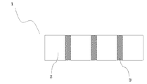
図1に実施形態に係るシンチレータアレイ1を例示する模式図を示した。図中、2はシンチレータセグメントである。前記シンチレータセグメント2は、立方体形状または直方体形状の焼結体である。前記シンチレータセグメント2のサイズは体積が1mm3以下であれば特に限定されるものではないが、縦、横、厚さがそれぞれ1mm以下であることが好ましい。前記シンチレータセグメント2を小型化することにより、検出される画像を高精細化することができる。
シンチレータアレイ1は、反射層3を介して複数個のシンチレータセグメント2を一体化したものである。
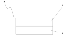
図2は実施形態の1例であるシンチレータアレイ1の反射層3の詳細図である。図中、1はシンチレータアレイ、2はシンチレータセグメント、3は反射層で、4は低屈折率誘電体材料層、5は高屈折率誘電体材料層、6は樹脂である。また、実施形態にかかるシンチレータアレイ1は、シンチレータセグメント2が体積1mm3以下と小型化されているため反射層3の厚みを100μm以下、さらには50μm以下と薄型化することも可能である。シンチレータアレイ1は、シンチレータセグメント2の間に、反射層3として、高屈折率誘電体材料層5と低屈折率誘電体材料層4との積層を1セットとして、これらを複数層積層しており、その間に樹脂6を介して接着されている。
FIG. 1 is a schematic view illustrating a
The
FIG. 2 is a detailed view of the
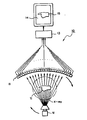
次にX線検出器について説明する。図3はX線検出器を例示する図である。図中、8はX線検出器、1はシンチレータアレイ、7は光電変換素子(検出素子)である。シンチレータアレイ1はX線入射面を有し、X線照射面とは反対側の面には光電変換素子7が一体的に設置されている。光電変換素子7としては、例えばフォトダイオードが使用される。光電変換素子7は、シンチレータアレイ1を構成するシンチレータセグメント2に対応する位置に配置されている。シンチレータアレイ1のX線入射面に表面反射層を設けてもよい。これらによって、X線検出器8が構成されている。図示はしていないが、シンチレータアレイ1に表面反射層を設けることによって、シンチレータアレイ1から放射される可視光の反射効率がさらに向上し、ひいてはシンチレータアレイ1の光出力を高めることができる。
Next, the X-ray detector will be described. FIG. 3 is a diagram illustrating an X-ray detector. In the figure, 8 is an X-ray detector, 1 is a scintillator array, and 7 is a photoelectric conversion element (detection element). The
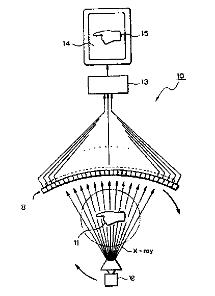
次にX線検査装置について説明する。図4は実施形態のX線検査装置の一例であるX線CT装置10を示している。図4において、10はX線CT装置、11は被検体、12はX線管、13はコンピュータ、14はディスプレイ、15は被検体画像である。X線CT装置10は、実施形態のX線検出器8を備えている。X線検出器8は被検体11の撮像部位を安置する円筒の内壁面に貼り付けられている。X線検出器8が貼り付けられた円筒の円弧の略中心には、X線を出射するX線管12が設置されている。X線検出器8とX線管12との間には被検体11が配置される。X線検出器8のX線入射面側には、図示しないコリメータが設けられている。
X線検出器8およびX線管12は、被検体11を中心にしてX線による撮影を行いながら回転するように構成されている。被検体11の画像情報が異なる角度から立体的に集められる。X線撮影により得られた信号(光電変換素子7により変換された電気信号)はコンピュータ13で処理され、ディスプレイ14上に被検体画像15として表示される。被検体画像15は、例えば被検体11の断層像である。図3に示すように、シンチレータセグメント2を2次元的に配置したシンチレータアレイ1を用いることによって、マルチ断層像タイプのX線CT装置10を構成することも可能である。この場合、被検体11の断層像が複数同時に撮影され、例えば撮影結果を立体的に描写することもできる。
図4に示すX線CT装置10は、実施形態のシンチレータアレイ1を有するX線検出器8を具備している。前述したように、実施形態のシンチレータアレイ1は反射層3の構成等に基づいて、シンチレータアレイ1から放射される可視光の反射効率が高いため、優れた光出力を有している。このようなシンチレータアレイ1を有するX線検出器8を使用することによって、X線CT装置10による撮影時間を短くすることができる。その結果、被検体11の被ばく時間を短くすることができ、低被ばく化を実現することが可能になる。実施形態のX線検査装置(X線CT装置10)は、人体の医療診断用のX線検査に限らず、動物のX線検査や工業用途のX線検査等に対しても適用可能である。
本発明の実施形態はX線非破壊検査装置による検査精度の向上などに対しても寄与するものである。
Next, an X-ray inspection apparatus will be described. FIG. 4 shows an X-ray CT apparatus 10 which is an example of the X-ray inspection apparatus of the embodiment. In FIG. 4, 10 is an X-ray CT apparatus, 11 is a subject, 12 is an X-ray tube, 13 is a computer, 14 is a display, and 15 is a subject image. The X-ray CT apparatus 10 includes the
The
An X-ray CT apparatus 10 shown in FIG. 4 includes an
The embodiment of the present invention also contributes to improvement of inspection accuracy by an X-ray nondestructive inspection apparatus.
(実施例1〜2、比較例1)
Gd2O2S:Pr(Pr濃度=0.05mol%)蛍光体粉末をラバープレスにより仮成形し、この成形体をTa製のカプセル中に脱気密封した後、これをHIP処理装置にセットした。HIP処理装置にアルゴンガスを加圧媒体として封入し、圧力147MPa、設定温度1425℃の条件で3時間処理した。このようにして、直径約80mm×高さ約120mmの円柱状の焼結体を作製した。
(Examples 1-2, Comparative Example 1)
Gd 2 O 2 S: Pr (Pr concentration = 0.05 mol%) phosphor powder was temporarily molded by rubber press, this molded body was deaerated and sealed in a Ta capsule, and then set in a HIP processing apparatus. did. Argon gas was sealed as a pressurized medium in the HIP processing apparatus, and the treatment was performed for 3 hours under conditions of a pressure of 147 MPa and a set temperature of 1425 ° C. In this way, a cylindrical sintered body having a diameter of about 80 mm and a height of about 120 mm was produced.
前記焼結体から、厚さ0.7mm×幅0.7mm×長さ0.8mmのシンチレータセグメントを長さ方向に100セグメント幅方向に30セグメントをマトリクス状に切り出して実施例および比較例に係るシンチレータアレイを作製した。
実施例および比較例に係るシンチレータアレイの製作工程は、下記の通りである。比較例は前記シンチレータセグメントを反射粒子と透明樹脂とから形成される幅方向および長さ方向に0.1mmの反射層を介して一体化した。実施例は前記シンチレータセグメントにスパッタ法により直接低屈折率誘電体材料層と高屈折誘電体材料層を交互に複数層(30層)成膜し、樹脂を介して一体化した。実施例および比較例の反射層の構成を表1に示す。
From the sintered body, scintillator segments having a thickness of 0.7 mm, a width of 0.7 mm, and a length of 0.8 mm are cut out in a lengthwise direction of 100 segments and a width of 30 segments in a widthwise direction in accordance with examples and comparative examples. A scintillator array was prepared.
The manufacturing process of the scintillator array according to the example and the comparative example is as follows. In the comparative example, the scintillator segments were integrated via a 0.1 mm reflective layer in the width direction and the length direction formed from the reflective particles and the transparent resin. In the example, a plurality of low-refractive-index dielectric material layers and high-refractive-index dielectric material layers were alternately formed on the scintillator segment by sputtering, and integrated through a resin. Table 1 shows the structures of the reflective layers of Examples and Comparative Examples.
実施例および比較例に係るシンチレータアレイについて、光出力、クロストークを測定した。これら測定値の測定結果を表2に示す。光出力の測定は、各シンチレータアレイをX線検出器にセットし、120kV、200mAのX線を照射した際に光電変換素子(検出素子)であるシリコンフォトダイオードに流れる電流値を光出力として求めた。このとき、比較例の電流値を100%として換算した%で示す。クロストークは、前記と同じX線をスリットを通して各シンチレータアレイに照射した際の、スリットを通したX線で発光したシンチレータセグメント(発光素子)に対する隣接したシンチレータセグメント(隣接素子)の出力比を発光素子の出力を100%として換算した%で示す。 The light output and crosstalk were measured for the scintillator arrays according to the example and the comparative example. Table 2 shows the measurement results of these measurement values. Optical output is measured by setting each scintillator array to an X-ray detector and calculating the value of the current flowing through a silicon photodiode as a photoelectric conversion element (detection element) as an optical output when irradiated with 120 kV and 200 mA X-rays. It was. At this time, it shows by% which converted the electric current value of the comparative example as 100%. Crosstalk emits the output ratio of the adjacent scintillator segment (adjacent element) to the scintillator segment (light emitting element) that emits light by the X-ray passing through the slit when the same X-rays as above are irradiated to each scintillator array through the slit. The element output is expressed as% converted to 100%.
この結果から、本発明の実施形態の一つである実施例によれば、比較例と比較して、クロストークが低減し、光出力が大きくなって向上している。 From this result, according to the example which is one of the embodiments of the present invention, compared with the comparative example, the crosstalk is reduced and the light output is increased and improved.
以上説明したように、本発明の実施形態のシンチレータアレイによれば、このように反射層を従来の白色反射粒子を含む反射層より薄くしても同等以上の反射率をもつためX線検出器1素子あたりの面積を小さくしても光漏れなどのノイズを低減することができ、X線CT装置の高解像度化が可能である。このように作製したシンチレータアレイは、十分な発光出力を有すると共に、光漏れが極めて小さいものとなり、X線検出器のシンチレータアレイとして極めて有用なものとなる。また、このようなX線検出器を用いたX線CT装置は、信号/ノイズ比が大きく、かつ診断能、空間分解能等に優れ、高解像度化が達成できる。
さらに、そのようなシンチレータアレイを使用することによって、解像度を高め、これにより医療診断能や非破壊検査精度の向上を図ったX線検出器およびX線検査装置を提供することが可能となる。
As described above, according to the scintillator array of the embodiment of the present invention, the X-ray detector has the same or higher reflectivity even if the reflective layer is made thinner than the conventional reflective layer containing white reflective particles. Even if the area per element is reduced, noise such as light leakage can be reduced, and the resolution of the X-ray CT apparatus can be increased. The scintillator array produced in this way has a sufficient light output and extremely small light leakage, making it extremely useful as a scintillator array for an X-ray detector. Further, an X-ray CT apparatus using such an X-ray detector has a large signal / noise ratio, is excellent in diagnostic ability, spatial resolution, etc., and can achieve high resolution.
Further, by using such a scintillator array, it is possible to provide an X-ray detector and an X-ray inspection apparatus that improve the resolution and thereby improve the medical diagnostic ability and the nondestructive inspection accuracy.
1…シンチレータアレイ
2…シンチレータセグメント
3…反射層
4…低屈折率誘電体材料層
5…高屈折率誘電体材料層
6…樹脂
7…光電変換素子(検出素子)
8…X線検出器
10…X線検査装置
11…被検体
12…X線管
13…コンピュータ
14…ディスプレイ
15…被検体画像
DESCRIPTION OF
8 ... X-ray detector 10 ...
Claims (13)
Priority Applications (1)
| Application Number | Priority Date | Filing Date | Title |
|---|---|---|---|
| JP2016012803A JP2017133894A (en) | 2016-01-26 | 2016-01-26 | Scintillator array and x-ray detector and x-ray inspection device using the same |
Applications Claiming Priority (1)
| Application Number | Priority Date | Filing Date | Title |
|---|---|---|---|
| JP2016012803A JP2017133894A (en) | 2016-01-26 | 2016-01-26 | Scintillator array and x-ray detector and x-ray inspection device using the same |
Publications (1)
| Publication Number | Publication Date |
|---|---|
| JP2017133894A true JP2017133894A (en) | 2017-08-03 |
Family
ID=59504913
Family Applications (1)
| Application Number | Title | Priority Date | Filing Date |
|---|---|---|---|
| JP2016012803A Pending JP2017133894A (en) | 2016-01-26 | 2016-01-26 | Scintillator array and x-ray detector and x-ray inspection device using the same |
Country Status (1)
| Country | Link |
|---|---|
| JP (1) | JP2017133894A (en) |
Cited By (1)
| Publication number | Priority date | Publication date | Assignee | Title |
|---|---|---|---|---|
| WO2021020491A1 (en) * | 2019-07-31 | 2021-02-04 | キヤノン株式会社 | Scintillator unit, and radiation detector |
-
2016
- 2016-01-26 JP JP2016012803A patent/JP2017133894A/en active Pending
Cited By (3)
| Publication number | Priority date | Publication date | Assignee | Title |
|---|---|---|---|---|
| WO2021020491A1 (en) * | 2019-07-31 | 2021-02-04 | キヤノン株式会社 | Scintillator unit, and radiation detector |
| US20220179105A1 (en) * | 2019-07-31 | 2022-06-09 | Canon Kabushiki Kaisha | Scintillator unit and radiation detector |
| US11774605B2 (en) * | 2019-07-31 | 2023-10-03 | Canon Kabushiki Kaisha | Scintillator unit and radiation detector |
Similar Documents
| Publication | Publication Date | Title |
|---|---|---|
| JP5587788B2 (en) | Radiation sensitive detector with scintillator in composite resin | |
| JP5089195B2 (en) | Radiation detection apparatus, scintillator panel, radiation detection system, and method for manufacturing radiation detection apparatus | |
| JP6911178B2 (en) | Scintillators, scintillator arrays, radiation detectors, and radiation inspection equipment | |
| US10281591B2 (en) | Ceramic scintillator array, X-ray detector, and X-ray inspection device | |
| JP6072232B2 (en) | Scintillator panel and manufacturing method thereof, radiation detector and manufacturing method thereof | |
| JP2007240306A (en) | Scintillator panel and plane detection unit | |
| US10416319B2 (en) | Ceramic scintillator array, method for manufacturing same, radiation detector and radiation inspection device | |
| US10684377B2 (en) | Scintillator, scintillator array, radiation detector, and radiation inspection device | |
| US10345456B2 (en) | Radiation detector and method for producing a radiation detector | |
| JP4764039B2 (en) | Phosphor sheet for radiation detector and radiation detector using the same | |
| JP4678924B2 (en) | Radiation detector and X-ray diagnostic apparatus using the same | |
| JP2017133894A (en) | Scintillator array and x-ray detector and x-ray inspection device using the same | |
| JP2006058099A (en) | Radiation scintillator and radiation image detector | |
| JP7451794B2 (en) | Scintillator array, scintillator array manufacturing method, radiation detector, and radiation inspection device | |
| JP2001208854A (en) | Radiation detector and medical image diagnosis device |