JP2017123764A - Electronic device - Google Patents
Electronic device Download PDFInfo
- Publication number
- JP2017123764A JP2017123764A JP2016002991A JP2016002991A JP2017123764A JP 2017123764 A JP2017123764 A JP 2017123764A JP 2016002991 A JP2016002991 A JP 2016002991A JP 2016002991 A JP2016002991 A JP 2016002991A JP 2017123764 A JP2017123764 A JP 2017123764A
- Authority
- JP
- Japan
- Prior art keywords
- cover
- substrate
- connector
- peripheral surface
- gap
- Prior art date
- Legal status (The legal status is an assumption and is not a legal conclusion. Google has not performed a legal analysis and makes no representation as to the accuracy of the status listed.)
- Pending
Links
Images
Landscapes
- Casings For Electric Apparatus (AREA)
- Connector Housings Or Holding Contact Members (AREA)
- Inverter Devices (AREA)
Abstract
【課題】電子機器において、基板の上方でカバーを貫通しているコネクタとカバーとの間の隙間からケース内部に異物が侵入し、当該異物が基板に落下することを防止するための技術を提供する。
【解決手段】電子機器は、上方が開口しているケースを塞ぐカバー7と、ケースに収容されカバー7の下方に配置されている基板5と、基板5から上方に延びており、カバー7の筒部71の内周面71aを貫通しているコネクタ2を備えている。カバー7と基板5との間でコネクタ2の外周面23aに鍔22が設けられており、内周面71aと外周面23aとの隙間9の直下で鍔22の上面に粘着剤26が備えられている。
【選択図】図2Provided is a technique for preventing foreign matter from entering a case through a gap between a connector penetrating the cover above the substrate and the cover in an electronic device and dropping the foreign matter onto the substrate. To do.
An electronic device includes a cover that closes a case that opens upward, a substrate that is accommodated in the case and disposed below the cover, and extends upward from the substrate. A connector 2 penetrating the inner peripheral surface 71a of the cylindrical portion 71 is provided. A flange 22 is provided on the outer peripheral surface 23 a of the connector 2 between the cover 7 and the substrate 5, and an adhesive 26 is provided on the upper surface of the flange 22 immediately below the gap 9 between the inner peripheral surface 71 a and the outer peripheral surface 23 a. ing.
[Selection] Figure 2
Description
本明細書が開示する技術は、ケースのカバーを貫通するように内側の基板からコネクタが延びている電子機器に関する。 The technology disclosed in this specification relates to an electronic device in which a connector extends from an inner board so as to penetrate a cover of a case.
一般に電子機器は、外部に位置する外部機器(例えば、コントローラ)と接続するために、コネクタを備える。例えば、特許文献1に、コネクタを備える電力変換装置が開示されている。 Generally, an electronic device includes a connector for connecting to an external device (for example, a controller) located outside. For example, Patent Document 1 discloses a power conversion device including a connector.
特許文献1の電力変換装置は、モータを収容する車載のトランスアスクルケースの上面に配置される。この電力変換装置は、トランスアスクルケースの上面に取り付けられている制御基板と、制御基板を覆うカバーで構成されている。この制御基板には、上方へ延びているコネクタが設けられており、コネクタはカバーを貫通している。 The power conversion device disclosed in Patent Document 1 is disposed on the upper surface of a vehicle-mounted trans-asscle case that houses a motor. This power conversion device is composed of a control board attached to the upper surface of the transaxle case and a cover that covers the control board. The control board is provided with a connector extending upward, and the connector penetrates the cover.
一般に、カバーを貫通するコネクタとカバーとの隙間は、この隙間からの水の侵入を防ぐためにシール部材等により封止されるが、海水等の塩を含んだ水がこの隙間に留まり続けると、この水によりコネクタが貫通している箇所でカバーが腐食する虞がある。特許文献1の電力変換装置では、コネクタは制御基板から上方に延びているので、コネクタとカバーとの隙間は、制御基板の上に位置している。そのため、カバーが腐食することにより発生する錆等の異物はこの隙間からカバーの内側へと侵入し、この異物が制御基板に落下する虞がある。本明細書は、電子機器において、基板から上方に延びてカバーを貫通しているコネクタとカバーとの間の隙間からケース内部に異物が侵入し、当該異物が基板に落下することを防止するための技術を提供する。 In general, the gap between the connector and the cover that penetrates the cover is sealed by a sealing member or the like to prevent water from entering from this gap, but when water containing salt such as seawater continues to remain in this gap, There is a possibility that the cover is corroded at a portion where the connector penetrates due to this water. In the power converter of Patent Document 1, since the connector extends upward from the control board, the gap between the connector and the cover is located on the control board. For this reason, foreign matter such as rust generated by corrosion of the cover may enter the inside of the cover through this gap, and this foreign matter may drop onto the control board. This specification is intended to prevent foreign matter from entering a case through a gap between a connector extending upward from a board and penetrating the cover and the cover and dropping the foreign substance onto the board in an electronic device. Provide technology.
本明細書が開示する電子機器は、上方に開口が設けられているケースと、開口を塞ぐカバーと、ケースに収容されており、カバーの下方に配置されている基板と、基板から上方に延びており、カバーに設けられている貫通孔を貫通しているコネクタを備えている。そして、カバーと基板との間でコネクタの外周面に鍔が設けられており、貫通孔の内周面とコネクタの外周面との隙間の直下で鍔の上面に粘着剤が備えられている。 An electronic device disclosed in this specification includes a case in which an opening is provided above, a cover that closes the opening, a substrate that is housed in the case and disposed below the cover, and extends upward from the substrate. And a connector penetrating through a through hole provided in the cover. A flange is provided on the outer peripheral surface of the connector between the cover and the substrate, and an adhesive is provided on the upper surface of the flange just below the gap between the inner peripheral surface of the through hole and the outer peripheral surface of the connector.
この構成によれば、貫通孔の内周面とコネクタの外周面との隙間からケースの内側に侵入する異物は、この隙間の直下で鍔の上面に備えられている粘着剤に付着し、鍔の下に位置する基板に落下しない。これにより、異物が基板に落下することを防止することができる。本明細書が開示する技術の詳細とさらなる改良は以下の「発明を実施するための形態」にて説明する。 According to this configuration, the foreign matter that enters the inside of the case through the gap between the inner peripheral surface of the through hole and the outer peripheral surface of the connector adheres to the adhesive provided on the upper surface of the ridge immediately below the gap, Do not fall on the substrate located under. Thereby, it can prevent that a foreign material falls to a board | substrate. Details and further improvements of the technology disclosed in this specification will be described in the following “DETAILED DESCRIPTION”.
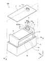
図面を参照して実施例の電子機器を説明する。本実施例の電子機器は、ハイブリッド車に搭載されるインバータ100である。インバータ100は、車載バッテリ(不図示)から供給される直流電力を走行用モータ(不図示)の駆動に適した交流電力に変換する。インバータ100は、ハイブリッド車のフロントコンパートメント内に配置される。図1は、インバータ100の分解斜視図である。なお、図中には、XYZ座標系が示されている。Z軸が、フロントコンパートメント内に配置されるインバータ100の上下方向、即ち、水平姿勢のハイブリッド車の上下方向と一致する。
An electronic apparatus according to an embodiment will be described with reference to the drawings. The electronic device of the present embodiment is an
インバータ100は、ケース4と、固定台3と、基板5と、パワーユニット6と、ケース4の上方(Z軸正方向)に設けられている開口4aを塞ぐカバー7を備えている。基板5とパワーユニット6が固定された固定台3がケース4の開口4aからケース4内に収容された後、カバー7が開口4aを塞ぐことにより、インバータ100が組み立てられる。ケース4とカバー7と固定台3は、アルミダイカスト製である。
The
固定台3は、X軸方向から見ると、上下方向に沿ったH字形状をしている。H字の形状の固定台3のうちのY軸方向に延びている平板3aの上面に、基板5が固定されており、平板3aの下面にパワーユニット6が固定されている。なお、平板3aの上面には、基板5を支持する複数の突条31が設けられており、各突条は平板3aのX軸方向の両端の間でX軸方向に延びている。
The fixed base 3 has an H shape along the vertical direction when viewed from the X-axis direction. The board |
パワーユニット6は、インバータ100のインバータ回路を構成している半導体素子とコンデンサが一つにまとめられたユニットである。図1では、パワーユニット6は、内部構成を省略して直方体で表されていることに留意されたい。パワーユニット6には、車載バッテリから延びているバッテリ側パワーケーブル(不図示)と、走行用モータから延びているモータ側パワーケーブル(不図示)が接続される。なお、インバータ100は、バッテリ側パワーケーブルとパワーユニット6を接続するための端子台と、モータ側パワーケーブルとパワーユニット6を接続するための端子台を備えているが、図1では、それら端子台の図示を省略している。
The
基板5は、パワーユニット6を駆動するための基板である。具体的には、基板5は、インバータ100の外部から供給される制御信号に従ってPWM信号を生成し、当該PWM信号をパワーユニット6の半導体素子のゲート端子に供給することによってパワーユニット6を駆動する。基板5の下面からはPWM信号を供給するための複数の信号線がパワーユニット6に向かって延びている。複数の信号線は、平板3aを貫通してパワーユニット6の半導体素子のゲート端子に接続されている。また、基板5の上面には、上方に延びているコネクタ2が設けられている。コネクタ2は、上記の複数の突条31の直上に配置されている。コネクタ2には、制御信号をインバータ100に供給するための信号ケーブルが接続される。基板5には、コネクタ2を介して、制御信号が供給される。
The
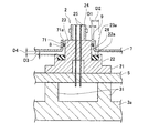
コネクタ2は、基板5に接続されている台座21と、鍔22と、台座21から上下方向に延びている柱状の延伸部23と、延伸部23の上面に設けられている筒部24を備えている。鍔22は、延伸部23の外周面23aに当該外周面23aを一巡するように設けられている。鍔22の上面には、当該上面を一巡するように、環状の溝22aが設けられている。溝22aには、粘着剤26が充填されている。筒部24の内側には、信号ピン25が上下方向に延びている。コネクタ2の延伸部23及び筒部24は、カバー7に設けられた筒部71の内側を貫通し、筒部24は、筒部71の上面からカバー7の外側に露出する。カバー7の外側に露出する筒部24に、上記の信号ケーブルの先端のコネクタが嵌合することにより、信号ピン25と信号ケーブルが接続される。なお、筒部71とコネクタ2の間には、Oリング8が配置される。
The
粘着剤26は、外気温及びインバータ100内の発熱により想定されるコネクタ2の周囲の温度域で粘着性が維持される材料である。例えば、粘着剤26は、この温度域より高い温度で硬化する熱硬化型の粘着性シリコンゲルである。
The
図2を参照して、コネクタ2の構成をさらに説明する。図2は、図1のII−II線における組み立て後のインバータ100の断面図においてコネクタ2の周囲を拡大した部分断面図である。図2に示すように、カバー7の筒部71の内周面71aと、コネクタ2の延伸部23の外周面23aの間は、Oリング8により封止される。内周面71aと外周面23aとOリング8は、いわゆる軸シール構造を構成する。また、筒部24の内側には、信号ピン25が上下方向に延びており、信号ピン25は延伸部23及び台座21の内部を貫通し、基板5に接続されている。信号ピン25は基板5に実装された回路と導通しているが、その回路は図示を省略している。
With reference to FIG. 2, the structure of the
鍔22は、延伸部23の外周面23aに設けられており、台座21の上面と繋がっている。図2に示されるように、インバータ100が組み立てられると、鍔22は、カバー7と基板5の間に配置される。環状の溝22aは、その内側面が延伸部23の外周面23aと面一となるように、鍔22の上面に設けられている。溝22aは、インバータ100が組み立てられると、カバー7の筒部71の内周面71aと延伸部23の外周面23aとの隙間9の直下に位置する。粘着剤26は、この溝22a内に充填されている。即ち、インバータ100が組み立てられると、粘着剤26は、隙間9の直下に位置する。ここで、溝22aの幅D2は、隙間9の幅D1よりも大きい。また、粘着剤26は、その上面が鍔22の上面から距離D3だけ下に位置するように充填される。そして、鍔22の上面は、カバー7の下面から距離D4だけ離れている。即ち、溝22aが設けられている鍔22の上面は、溝22aに充填されている粘着剤26の上面より高くなっており、鍔22の上面は、カバー7の下面から離れている。
The
本実施例の効果について説明する。インバータ100はハイブリッド車のフロントコンパートメント内に配置されているので、ハイブリッド車の走行環境によって、海水等の塩を含んだ水に曝される。上記のように、カバー7とコネクタ2の隙間9は、Oリング8により封止されている。これにより、隙間9からケース4の内側に水が侵入することが防止される。しかし、Oリング8は軸シール構造であり、隙間9は上方に開口している。そのため、上方から隙間9に入り込んだ塩を含んだ水が、隙間9のうちのOリング8より上方の空間に溜まる場合がある。この空間に水が留まり続けると、カバー7の筒部71の内周面71aが、この水により腐食する虞がある。この場合、内周面71aが腐食することにより発生する錆等の異物が隙間9からカバー7の下方に落下し得る。
The effect of the present embodiment will be described. Since the
実施例の構成によれば、隙間9からカバー7の下方に落下する異物は、隙間9の直下で鍔22の上面に位置している粘着剤26に付着し、鍔22の下に位置している基板5の上面に落下しない。これにより、異物が基板5に落下することを防止することができる。さらに、上記のように、溝22aの幅D2が、隙間9の幅D1よりも大きいことにより、隙間9から侵入する異物を的確に粘着剤26に付着させることができる。
According to the configuration of the embodiment, the foreign matter falling from the
また、上記のように、溝22aが設けられている鍔22の上面は、粘着剤26の上面より高くなっており、鍔22の上面は、カバー7の下面から離れている。これにより、粘着剤26がカバー7の下面に接することを防止することができる。特に、メンテナンス等によりカバー7をケース4から取り外す場合でも、粘着剤26がカバー7に粘着して溝22aから剥がれ、剥がれた粘着剤26の一部が基板5に落下することを防止することができる。
Further, as described above, the upper surface of the
以下、実施例で示した技術に関する留意点を述べる。溝22aは、設けられなくてもよい。この場合、鍔22の上面に直接に粘着剤26が備えられていてもよい。
Hereinafter, points to be noted regarding the technology shown in the embodiments will be described. The
以上、本発明の具体例を詳細に説明したが、これらは例示に過ぎず、特許請求の範囲を限定するものではない。特許請求の範囲に記載の技術には、以上に例示した具体例を様々に変形、変更したものが含まれる。本明細書または図面に説明した技術要素は、単独であるいは各種の組合せによって技術的有用性を発揮するものであり、出願時請求項記載の組合せに限定されるものではない。また、本明細書または図面に例示した技術は複数目的を同時に達成し得るものであり、そのうちの一つの目的を達成すること自体で技術的有用性を持つものである。 Specific examples of the present invention have been described in detail above, but these are merely examples and do not limit the scope of the claims. The technology described in the claims includes various modifications and changes of the specific examples illustrated above. The technical elements described in this specification or the drawings exhibit technical usefulness alone or in various combinations, and are not limited to the combinations described in the claims at the time of filing. In addition, the technology exemplified in this specification or the drawings can achieve a plurality of objects at the same time, and has technical usefulness by achieving one of the objects.
2:コネクタ
3:固定台
4:ケース
4a:ケースの開口
5:基板
6:パワーユニット
7:カバー
8:Oリング
9:隙間
21:台座
22:鍔
22a:溝
23:延伸部
23a:延伸部の外周面
24:筒部
25:信号線
26:粘着剤
71:カバーの筒部
71a:筒部の内周面
100:インバータ
2: Connector 3: Fixing base 4:
Claims (1)
前記開口を塞ぐカバーと、
前記ケースに収容されており、前記カバーの下方に配置されている基板と、
前記基板から上方に延びており、前記カバーに設けられている貫通孔を貫通しているコネクタと、
を備えており、
前記カバーと前記基板との間で前記コネクタの外周面に鍔が設けられており、
前記貫通孔の内周面と前記コネクタの外周面との隙間の直下で前記鍔の上面に粘着剤が備えられている、
ことを特徴とする電子機器。 A case where an opening is provided above;
A cover for closing the opening;
A substrate housed in the case and disposed below the cover;
A connector extending upward from the substrate and penetrating a through hole provided in the cover;
With
A flange is provided on the outer peripheral surface of the connector between the cover and the substrate,
An adhesive is provided on the upper surface of the flange just below the gap between the inner peripheral surface of the through hole and the outer peripheral surface of the connector.
An electronic device characterized by that.
Priority Applications (1)
| Application Number | Priority Date | Filing Date | Title |
|---|---|---|---|
| JP2016002991A JP2017123764A (en) | 2016-01-08 | 2016-01-08 | Electronic device |
Applications Claiming Priority (1)
| Application Number | Priority Date | Filing Date | Title |
|---|---|---|---|
| JP2016002991A JP2017123764A (en) | 2016-01-08 | 2016-01-08 | Electronic device |
Publications (1)
| Publication Number | Publication Date |
|---|---|
| JP2017123764A true JP2017123764A (en) | 2017-07-13 |
Family
ID=59306405
Family Applications (1)
| Application Number | Title | Priority Date | Filing Date |
|---|---|---|---|
| JP2016002991A Pending JP2017123764A (en) | 2016-01-08 | 2016-01-08 | Electronic device |
Country Status (1)
| Country | Link |
|---|---|
| JP (1) | JP2017123764A (en) |
-
2016
- 2016-01-08 JP JP2016002991A patent/JP2017123764A/en active Pending
Similar Documents
| Publication | Publication Date | Title |
|---|---|---|
| AU2023100025A4 (en) | Module for connecting a mast to a board | |
| CA2986550C (en) | Drive device | |
| CN106208622A (en) | The power converter being merged in housing | |
| JP2009201218A (en) | Hybrid drive device | |
| JP6048427B2 (en) | Electronic equipment | |
| CN104796008B (en) | Semiconductor device | |
| CN210110884U (en) | Battery pack box, battery pack and vehicle | |
| CN106972705A (en) | drive device | |
| JP5515756B2 (en) | Power converter | |
| JP2013077500A (en) | Battery pack | |
| WO2014178342A1 (en) | Vehicle-mounted power conversion device | |
| JP2015073365A (en) | Power supply device, lamp and vehicle | |
| JP2016116274A (en) | Controller integrated electrical rotating machine | |
| US8885352B2 (en) | Power supply module of linear actuator and conversion assembly thereof | |
| JP5853930B2 (en) | Power control unit | |
| JPH09277840A (en) | High-power box structure of electric vehicle and method of assembling high-power box | |
| CN203261606U (en) | DC motor controller | |
| CN205545045U (en) | Motor controller | |
| JP2016067096A (en) | Power converter | |
| CN214957207U (en) | Battery box extension structure | |
| JP3196598U (en) | Railway model and electric board | |
| JP7310593B2 (en) | power converter | |
| CN102892271A (en) | Heat radiating housing of controller of electric vehicle | |
| JP2016082000A (en) | Electrical equipment | |
| CN218498293U (en) | Battery box and battery device |