JP2017123733A - Electric connection box - Google Patents
Electric connection box Download PDFInfo
- Publication number
- JP2017123733A JP2017123733A JP2016001775A JP2016001775A JP2017123733A JP 2017123733 A JP2017123733 A JP 2017123733A JP 2016001775 A JP2016001775 A JP 2016001775A JP 2016001775 A JP2016001775 A JP 2016001775A JP 2017123733 A JP2017123733 A JP 2017123733A
- Authority
- JP
- Japan
- Prior art keywords
- coil
- bus bar
- mounting surface
- case
- circuit board
- Prior art date
- Legal status (The legal status is an assumption and is not a legal conclusion. Google has not performed a legal analysis and makes no representation as to the accuracy of the status listed.)
- Pending
Links
- 229920005989 resin Polymers 0.000 claims abstract description 11
- 239000011347 resin Substances 0.000 claims abstract description 11
- 230000004308 accommodation Effects 0.000 claims description 5
- 238000003780 insertion Methods 0.000 claims description 4
- 230000037431 insertion Effects 0.000 claims description 4
- 206010037660 Pyrexia Diseases 0.000 claims 1
- 239000000126 substance Substances 0.000 abstract 1
- 238000004804 winding Methods 0.000 description 9
- 239000000945 filler Substances 0.000 description 8
- 239000000853 adhesive Substances 0.000 description 6
- 230000001070 adhesive effect Effects 0.000 description 6
- 238000005516 engineering process Methods 0.000 description 5
- 239000000463 material Substances 0.000 description 5
- 238000005452 bending Methods 0.000 description 4
- 229910052751 metal Inorganic materials 0.000 description 4
- 239000002184 metal Substances 0.000 description 4
- 229920003002 synthetic resin Polymers 0.000 description 4
- 239000000057 synthetic resin Substances 0.000 description 4
- RYGMFSIKBFXOCR-UHFFFAOYSA-N Copper Chemical compound [Cu] RYGMFSIKBFXOCR-UHFFFAOYSA-N 0.000 description 3
- 230000017525 heat dissipation Effects 0.000 description 3
- 239000007788 liquid Substances 0.000 description 3
- 230000005855 radiation Effects 0.000 description 3
- 229910000881 Cu alloy Inorganic materials 0.000 description 2
- 229910052782 aluminium Inorganic materials 0.000 description 2
- XAGFODPZIPBFFR-UHFFFAOYSA-N aluminium Chemical compound [Al] XAGFODPZIPBFFR-UHFFFAOYSA-N 0.000 description 2
- 229910052802 copper Inorganic materials 0.000 description 2
- 239000010949 copper Substances 0.000 description 2
- 230000004907 flux Effects 0.000 description 2
- 238000000034 method Methods 0.000 description 2
- 230000002093 peripheral effect Effects 0.000 description 2
- 229910000838 Al alloy Inorganic materials 0.000 description 1
- 230000002159 abnormal effect Effects 0.000 description 1
- 239000011889 copper foil Substances 0.000 description 1
- 238000004512 die casting Methods 0.000 description 1
- 230000000694 effects Effects 0.000 description 1
- 239000002320 enamel (paints) Substances 0.000 description 1
- 239000003822 epoxy resin Substances 0.000 description 1
- 238000010438 heat treatment Methods 0.000 description 1
- 238000002347 injection Methods 0.000 description 1
- 239000007924 injection Substances 0.000 description 1
- 239000011810 insulating material Substances 0.000 description 1
- 239000000696 magnetic material Substances 0.000 description 1
- 230000035699 permeability Effects 0.000 description 1
- 229920000647 polyepoxide Polymers 0.000 description 1
- 238000003825 pressing Methods 0.000 description 1
- 238000004080 punching Methods 0.000 description 1
- 229920001187 thermosetting polymer Polymers 0.000 description 1
- 239000011345 viscous material Substances 0.000 description 1
- 229910000859 α-Fe Inorganic materials 0.000 description 1
Images

Landscapes
- Mounting Components In General For Electric Apparatus (AREA)
- Casings For Electric Apparatus (AREA)
- Cooling Or The Like Of Electrical Apparatus (AREA)
- Connection Or Junction Boxes (AREA)
Abstract
Description
本明細書に記載される技術は、電気接続箱に関する。 The technology described herein relates to an electrical junction box.
自動車等の車両には、DC−DCコンバータ等の電気接続箱が搭載されており、この電気接続箱等の回路部品としてコイルが用いられている。特許文献1の電気接続箱は、合成樹脂製の枠状部材が放熱部材の外周部に被せられており、この枠状部材には、回路基板が収容されるとともに、枠状部材の区画された部分にチョークコイルが配されている。 An electric junction box such as a DC-DC converter is mounted on a vehicle such as an automobile, and a coil is used as a circuit component of the electric junction box. In the electric junction box of Patent Document 1, a frame-shaped member made of synthetic resin is put on the outer peripheral portion of the heat radiating member. The frame-shaped member accommodates the circuit board and is partitioned by the frame-shaped member. A choke coil is arranged in the part.
ところで、放熱部材の上においてコイルが配される領域は、他の電子部品を実装することができないため、他の電子部品を実装するための領域を電気接続箱内に確保しなければならず、電気接続箱の小型化が容易ではなかった。特に、大電流の通電が可能なコイルを電気接続箱に搭載すると、コイルが大型化することにより、コイルが占める領域が大きくなり、電気接続箱が大型化しやすいという問題がある。 By the way, since the region where the coil is arranged on the heat dissipation member cannot mount other electronic components, the region for mounting other electronic components must be secured in the electrical junction box. It was not easy to downsize the electrical junction box. In particular, when a coil capable of energizing a large current is mounted on an electrical junction box, there is a problem that the area occupied by the coil increases due to the increase in size of the coil, and the electrical junction box is likely to be enlarged.
本明細書に記載された技術は上記のような事情に基づいて完成されたものであって、電気接続箱を小型化することを目的とする。 The technology described in the present specification has been completed based on the above-described circumstances, and aims to reduce the size of the electrical junction box.
本明細書に記載された電気接続箱は、外部と接続可能な端子部を有するコイルと磁性体のコアとがケースに収容されてなるコイル装置と、バスバーを有する回路基板と、前記コイル装置及び前記回路基板が載置される載置面と、を備える電気接続箱であって、前記回路基板は、前記載置面に接着されており、前記バスバーは、前記端子部と接続されるバスバー端子と、前記バスバー端子側が曲げられた状態の曲げ部と、を有しており、前記コイルは、前記載置面に沿う平面を通る軸を中心に巻回されており、前記ケース内には絶縁性の樹脂からなる充填部が充填されている。
本構成によれば、コイルは、載置面に沿う平面を通る軸を中心に巻回されているため、例えば、載置面に沿う平面に直交する軸を中心に巻回されたコイルを有するコイル装置を載置面に載置する構成と比較して、載置面上に占めるコイル装置の領域を小さくすることが可能になる。これにより、コイル装置が占有していた領域を他の電子部品の実装のために利用することができるため、電気接続箱を小型化することが可能になる。
また、ケース内は、絶縁性の樹脂からなる充填部が充填されているため、コイルの振動による異音を抑制することができる。
更に、バスバーは、バスバー端子側に曲げ部を有するため、バスバー端子側がストレートな形状で延びる構成と比較して振動を曲げ部によって吸収することができる。これにより、回路基板側等からの振動を曲げ部で吸収することができるため、回路基板側等の振動が充填部に伝わることによる充填部の割れ等を抑制することができる。
An electrical junction box described in the present specification includes a coil device in which a coil having a terminal portion connectable to the outside and a magnetic core are housed in a case, a circuit board having a bus bar, the coil device, An electric connection box including a mounting surface on which the circuit board is mounted, wherein the circuit board is bonded to the mounting surface, and the bus bar is a bus bar terminal connected to the terminal portion. And a bent portion in a state where the bus bar terminal side is bent, and the coil is wound around an axis passing through a plane along the mounting surface, and is insulated in the case. A filling portion made of a conductive resin is filled.
According to this configuration, since the coil is wound around an axis passing through a plane along the placement surface, for example, the coil has a coil wound around an axis orthogonal to the plane along the placement surface. Compared to the configuration in which the coil device is placed on the placement surface, the area of the coil device that occupies the placement surface can be reduced. Thereby, since the area | region which the coil apparatus occupied can be utilized for mounting of another electronic component, it becomes possible to reduce an electrical junction box.
Moreover, since the filling part which consists of insulating resin is filled in the case, the noise by the vibration of a coil can be suppressed.
Furthermore, since the bus bar has a bent portion on the bus bar terminal side, vibration can be absorbed by the bent portion as compared with a configuration in which the bus bar terminal side extends in a straight shape. Thereby, since the vibration from the circuit board side etc. can be absorbed in a bending part, the crack of the filling part etc. by vibration on the circuit board side etc. being transmitted to a filling part can be suppressed.
本明細書に記載された技術の実施態様としては以下の態様が好ましい。
前記コイルは、平角線の短辺側を内径面とするように巻回されたエッジワイズコイルである。
このようにすれば、コイルに大電流の通電が可能となるとともに、コイルの軸方向の長さを短くすることができるため、より一層、載置面上に占めるコイル装置の領域を小さくすることが可能になる。
The following embodiments are preferable as the embodiments of the technology described in this specification.
The coil is an edgewise coil wound so that the short side of the rectangular wire is the inner diameter surface.
In this way, the coil can be energized with a large current, and the length of the coil in the axial direction can be shortened. Therefore, the area of the coil device on the mounting surface can be further reduced. Is possible.
前記載置面は、前記コイル装置の熱を放熱する放熱部材に設けられているとともに、前記載置面には、前記コイル装置が収容される収容凹部が形成されている。
このようにすれば、収容凹部にコイル装置が収容されることで、放熱部材におけるコイル装置の熱を受ける面積が大きくなるため、コイル装置の熱を効率良く放熱部材に伝えることができる。また、収容凹部に収容されたコイル装置のケース内には、絶縁性の樹脂からなる充填部が充填されているため、放熱部材に対するコイルの絶縁を確実に行うことができる。
The mounting surface is provided on a heat radiating member that dissipates heat of the coil device, and an accommodation recess in which the coil device is accommodated is formed on the mounting surface.
In this way, since the coil device is housed in the housing recess, the area of the heat radiating member that receives heat from the coil device is increased, so that the heat of the coil device can be efficiently transmitted to the heat radiating member. In addition, since the case of the coil device housed in the housing recess is filled with a filling portion made of an insulating resin, the coil can be reliably insulated from the heat radiating member.
前記ケース及び前記収容凹部の一方には、ガイド溝が設けられ、前記ケース及び前記収容凹部の他方には、前記ガイド溝に係合して前記コイル装置の前記収容凹部内への挿入方向を案内するガイドリブが設けられている。
このようにすれば、ガイド溝とガイドリブとが係合することによりコイル装置の収容凹部への挿入の案内及び位置決めを行うことが可能になる。
One of the case and the receiving recess is provided with a guide groove, and the other of the case and the receiving recess is engaged with the guide groove to guide the insertion direction of the coil device into the receiving recess. Guide ribs are provided.
If it does in this way, it will become possible to perform guidance and positioning of insertion to the accommodation crevice of a coil device by engaging a guide slot and a guide rib.
本明細書に記載された技術によれば、電気接続箱を小型化することが可能になる。 According to the technique described in this specification, it is possible to reduce the size of the electrical junction box.
<実施形態1>
実施形態1の電気接続箱10について、図1〜図9を参照して説明する。
本実施形態の電気接続箱10は、例えば、電気自動車やハイブリッド自動車等の車両のバッテリ等の電源と、ランプ、ワイパー等の車載電装品やモータ等からなる負荷との間の電力供給経路に配され、例えばDC−DCコンバータやインバータ等に用いることができる。以下では、X方向を右方、Y方向を前方、Z方向を上方として説明する。
<Embodiment 1>
The
The
(電気接続箱10)
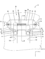
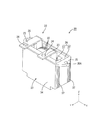
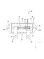
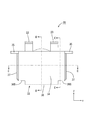
電気接続箱10は、図3に示すように、電子部品(図示しない)が実装された回路体11と、コイル装置20と、回路体11及びコイル装置20の熱を放熱する放熱部材40と、放熱部材40の上方側を覆うカバー60と、を備えている。
(カバー60)
カバー60は、下方側が開口した箱形であって、放熱部材40に図示しないネジによりネジ留めされて固定されている。
(Electric junction box 10)
As shown in FIG. 3, the
(Cover 60)
The
(回路体11)
回路体11は、回路基板11Aと、回路基板11Aに実装される電子部品とを備える。回路基板11Aは、放熱部材40の載置面41上に接着されており、プリント基板12と、プリント基板12に重ねられたバスバー13とを備える。プリント基板12は、絶縁材料からなる絶縁板に銅箔からなる導電路(図示しない)がプリント配線技術により形成されている。バスバー13は、銅や銅合金等の金属板材を導電路に応じた形状に打ち抜いて形成されている。バスバー13の端部側は、プリント基板12の周縁の外側に延びており、共にほぼ直角に曲げられた第1曲げ部13A(「曲げ部」の一例)と第2曲げ部13B(「曲げ部」の一例)とが連なってクランク状に屈曲されている。第1曲げ部13A及び第2曲げ部13Bにより、第2曲げ部13Bよりも先の先端部は、プリント基板12側の載置面41に接着されたバスバー13とは異なる高さの位置にバスバー端子14が形成されている。バスバー端子14には、円形状の接続孔14Aが貫通形成されている。プリント基板12とバスバー13は、例えば、接着剤、接着シート等により貼り合わせて構成されている。
(Circuit body 11)
The
(コイル装置20)
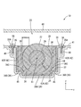
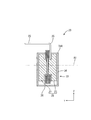
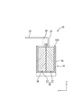
コイル装置20は、例えば出力電圧を平滑化するチョークコイルであって、コイル21と、磁性体のコア26と、コイル21及びコア26を収容するケース33と、ケース33に充填された充填部38とを備える。
(Coil device 20)
The
(コイル21)
コイル21は、いわゆるエッジワイズコイルであって、例えば銅又は銅合金からなり、扁平な矩形状の断面を有する帯状の平角線を、短辺側が内径面及び外径面となるように螺旋状に巻回して形成したものであり、外面にはエナメル被覆が施されている。このコイル21は、軸A1を中心に円形状に複数回(本実施形態では4回)巻回された巻回部22と、外部と接続される一対の端子部23と、巻回部22と端子部23との間でL字状に曲げられた曲げ部25と、を有する。
(Coil 21)
The
複数の巻回部22は、内径及び外径が一定で巻回されており、この巻回部22により、コイル21は、軸A1の方向に弾性変形可能な形状となっている。一対の端子部23は、共に直線状で互いに平行に配置されている。端子部23の先端部には、締結部材としてのボルト53の軸部が挿通可能な円形状の接続孔24が貫通形成されている。曲げ部25は、巻回部22と端子部23との間を直角に接続しているため、一対の端子部23の延出方向は、後述する放熱部材40の載置面41と実質的に平行な方向(載置面41に沿う方向)とされている。
The plurality of winding
(コア26)
コア26は、フェライト等の高透磁率の磁性体で形成されており、一対の分割部材27,27を組み合わせて構成されている。各分割部材27,27は、図7に示すように、円柱状の柱部29と、円弧状に湾曲した内面を有する側壁部30と、柱部29と側壁部30を連結してコイル21を支持する板状の連結支持部31と、を備え、これらが一体に形成されている。
(Core 26)
The
(ケース33)
ケース33は、絶縁性を有する合成樹脂製であって、図5,図8に示すように、角筒状の角筒部34と、角筒部34を閉鎖する奥壁部36とを備えている。角筒部34の前端部には、コイル21が装着されたコア26を挿通可能な長方形状の開口部34Aが形成されており、角筒部34の前端部は、外方側に張り出す張出部35が形成されている。張出部35には、ネジ56の軸部が挿通される通し孔35Aが貫通形成されており、図2に示すように、放熱部材40の載置面41に凹設された留め部48にネジ56でネジ留めされる。奥壁部36は、角筒部34の背面を隙間なく覆っており、巻回部22の形状に応じて外方に突出する凸部36Aと、凸部36Aよりも凹んだ凹部36Bとが形成されている。凹部36Bの内面側は、コア26を受ける受け部36Cとされている。コア26が受け部36Cに載置されることで、ケース33内におけるコア26の位置決めがされる。角筒部34の左右の外側面には、図7に示すように、それぞれ一対のガイドリブ37が上下方向に延びている。ガイドリブ37は、角筒部34の側壁の長さの全体に亘って延びている。
(Case 33)
The
(充填部38)
充填部38は、図2に示すように、ケース33内におけるコイル21とコア26が配されない空間の隙間を埋めるように充填材が充填されたものであり、コイル21とコア26との間の隙間、コア26とケース33との間の隙間等に入り込んでいる。本実施形態では、充填材は、例えば、エポキシ樹脂が用いられているが、これに限られず、他の公知の材料等を用いることも可能である。充填材は、ケース33への注入時には、液体である。例えばケース33への注入後に加熱により固化する熱硬化性樹脂や、加熱せずに硬化する常温硬化型の樹脂を用いてもよい。また、充填材は、ケース33への注入後に硬化せずに、ある程度、形状を保持できる程度の粘性を有する材料を用いてもよい。充填材の粘性は、コイル21やコア26との間の隙間に液体の状態の充填材が浸入する程度の粘性を有するものとすることができ、コイル21やコア26等の隙間の寸法に応じて適切な粘性の材料を使用することができる。
(Filling part 38)
As shown in FIG. 2, the filling
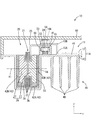
(放熱部材40)
放熱部材40は、例えば、アルミダイカスト等で成形されるアルミニウム、アルミニウム合金等の熱伝導性が高い金属類製であって、図3に示すように、上面は、コイル装置20及び回路体11が載置される載置面41とされ、下面側には複数の放熱フィン49が櫛歯状に並んでいる。
(Heat dissipation member 40)
The
載置面41は、回路体11が載置される平坦な領域を有するとともに、他の領域に収容凹部42が窪み形成されている。収容凹部42は、コイル装置20が載置される底面42Aと、コイル装置20の側面に対向する壁面42Bとを備え、放熱部材40に略直方体状の空間を形成する。図2に示すように、収容凹部42の底面42Aには、ケース33の凹部36Bに応じた突部45が形成されている。左右の壁面42Bの上部には、ケース33の張出部35をネジ留め可能な留め部48が形成されている。留め部48は、載置面41から張出部35の寸法に応じて窪み形成されており、ネジ56でネジ留め可能とされている。収容凹部42の左右の壁面42Bには、それぞれ一対のガイドリブ37に係合する一対のガイド溝44(図1参照)が上下方向に延びている。
The
載置面41には絶縁層(図示しない)が積層されており、放熱部材40と回路体11との間を絶縁する。絶縁層は、液状の接着剤等の樹脂が硬化することで形成され、熱伝導性が高く、絶縁性を有する材料が用いられる。載置面41上に絶縁性の接着剤を塗布した状態で、載置面41の(接着剤の)上に回路基板11Aを載置し、例えば治具等を用いて回路基板11Aを載置面41側に押し付けることで回路基板11Aを載置面41に接着することができる。載置面41上におけるコイル装置20の近傍には、図3に示すように、端子台50が固定されている。端子台50は、絶縁性の合成樹脂からなり、端子部23の高さに応じた所定の高さで形成されている。端子台50にはナット54の回転を規制した状態で保持する保持凹部51が形成されており、この保持凹部51は、ボルト53の軸部を逃げる形状とされている。端子台50の上面には、図1に示すように、端子部23が挿通されて左右方向に位置決めする位置決め部52が上方に突出している。端子台50上にバスバー端子14と端子部23とを重ねて配し、締結部材としてのボルト53とナット54で締結することで、バスバー端子14と端子部23との間が接続されて固定される。なお、端子台50は、独立した部品とすることができるが、これに限られず、例えば、放熱部材40の外縁部に被せられる図示しないフレームに一体に形成してもよい。
An insulating layer (not shown) is stacked on the mounting
次に、コイル装置20の組み付けについて説明する。
コア26を構成する一方の分割部材27にコイル21を載置し、上下の分割部材27,27を嵌め合わせ、この状態のコイル21及びコア26をケース33に収容する(図4)。次に、ケース33の開口部34Aから図示しない注入機により充填材を注入する。ケース33の所定の深さまで充填材が充填されたら、注入を終了する。充填材が固化すると充填部38が形成されてコイル装置20が形成される。次に、コイル装置20を放熱部材40の収容凹部42にガイドリブ37をガイド溝44に係合させつつ挿入する。コイル装置20を所定の深さまで挿入すると、端子部23が端子台50の上に配される。そして、張出部35を留め部48にネジ56でネジ留めするとともに、放熱部材40の載置面41に塗布された接着剤上に回路体11を載置すると、回路体11のバスバー端子14とコイル21の端子部23が重なった状態となる。そして、ボルト53とナット54でバスバー端子14と端子部23とを締結する。これにより、コイル装置20が組み付けられた状態の電気接続箱10となる。
Next, assembly of the
The
本実施形態によれば、以下の作用・効果を奏する。
本実施形態の電気接続箱10は、外部と接続可能な端子部23を有するコイル21と磁性体のコア26とがケース33に収容されてなるコイル装置20と、バスバー13を有する回路基板11Aと、コイル装置20及び回路基板11Aが載置される載置面41と、を備える電気接続箱10であって、回路基板11Aは、載置面41に接着されており、バスバー13は、端子部23と接続されるバスバー端子14と、バスバー端子14側が曲げられた状態の曲げ部13A,13Bと、を有し、コイル21は、載置面41に沿う平面を通る軸A1を中心に巻回されており、ケース33内には絶縁性の樹脂からなる充填部38が充填されている。
According to the present embodiment, the following operations and effects are achieved.
The
本実施形態によれば、コイル21は、載置面41に沿う平面を通る軸A1を中心に巻回されているため、例えば、載置面41に沿う平面に直交する軸A1を中心に巻回されたコイル21を有するコイル装置20と比較して、載置面41上に占めるコイル装置20の領域を小さくすることが可能になる。これにより、コイル装置20が占有していた領域を他の電子部品の実装のために利用することができるため、電気接続箱10を小型化することが可能になる。
また、ケース33内は、樹脂からなる充填部38で充填されているため、コイル21の振動による異音を抑制することができる。
更に、バスバー13は、バスバー端子14側に曲げ部13A,13Bを有するため、バスバー端子14側がストレートに延びる構成と比較して曲げ部13A,13Bが振動を吸収することができる。これにより、回路基板11A側等からの振動が充填部38に伝わることによる充填部38の割れ等を抑制することができる。
According to the present embodiment, since the
Moreover, since the inside of the
Furthermore, since the
また、コイル21は、平角線の短辺側を内径面とするように巻回されたエッジワイズコイル21である。
このようにすれば、コイル21に大電流の通電が可能となるとともに、コイル21の軸A1の方向の長さを短くすることができるため、より一層、載置面41上に占めるコイル装置20の領域を小さくすることが可能になる。
The
In this way, the
また、載置面41は、コイル装置20の熱を放熱する放熱部材40に設けられているとともに、載置面41には、コイル装置20が収容される収容凹部42が形成されている。
このようにすれば、収容凹部42にコイル装置20が収容されることで、放熱部材40におけるコイル装置20の熱を受ける面積が大きくなるため、コイル装置20の熱を効率良く放熱部材40に伝えることができる。また、ケース33内には、絶縁性の樹脂からなる充填部38が充填されているため、放熱部材40に対するコイル21の絶縁を確実に行うことができる。また、コイル装置20の外側が放熱部材40の金属で覆われることになるため、磁性体のギャップから発生する漏れ磁束が金属で遮蔽される。これにより、漏れ磁束による他の電子部品への影響を抑制することができる。
In addition, the mounting
If the
また、(ケース33及び)収容凹部42(の一方)には、ガイド溝44が設けられ、ケース33(及び収容凹部42の他方)には、ガイド溝44に係合してコイル装置の収容凹部42内への挿入方向を案内するガイドリブ37が設けられている。
このようにすれば、ガイド溝44とガイドリブ37とが係合することによりコイル装置20の収容凹部42内への挿入の案内及び位置決めを行うことが可能になる。
Further, a
In this way, the
<他の実施形態>
本明細書に記載された技術は、上記記述及び図面によって説明した実施形態に限定されるものではなく、例えば次のような実施形態も本明細書に記載された技術の技術的範囲に含まれる。
(1)絶縁性の合成樹脂等からなるボビンを備える構成とし、ボビンでコイル21とコア26との間を保持する構成としてもよい。
<Other embodiments>
The technology described in the present specification is not limited to the embodiments described with reference to the above description and drawings. For example, the following embodiments are also included in the technical scope of the technology described in the present specification. .
(1) It is good also as a structure provided with the bobbin which consists of an insulating synthetic resin etc., and it is good also as a structure which hold | maintains between the
(2)コイル装置20は、出力電圧を平滑化するチョークコイルとしたが、他の用途に用いられるコイル装置としてもよい。
(2) Although the
(3)巻回部22が巻回される回数は、上記実施形態の回数に限られない。例えば、1〜3回、5回以上としてもよい。但し、巻回部22が巻回される回数が少ない方がコイル装置20における軸A1の方向の寸法を小さくできるため、より電気接続箱10を小型化することができる。
(3) The number of times the winding
(4)収容凹部42にガイド溝44を設け、ケース33にガイドリブ37が設けたがこれに限られず、ケース33にガイド溝を設け、収容凹部にガイドリブ37を設けてもよい。
(4) Although the
10: 電気接続箱
11:回路部
11A:回路基板
12:プリント基板
13:バスバー
13A:第1曲げ部(曲げ部)
13B:第2曲げ部(曲げ部)
14: バスバー端子
20: コイル装置
21: コイル
23: 端子部
26: コア
33: ケース
37: ガイドリブ
38: 充填部
40: 放熱部材
41: 載置面
42: 収容凹部
44: ガイド溝
50: 端子台
53: ボルト
54: ナット
10: Electrical connection box 11:
13B: 2nd bending part (bending part)
14: Busbar terminal 20: Coil device 21: Coil 23: Terminal part 26: Core 33: Case 37: Guide rib 38: Filling part 40: Heat radiating member 41: Mounting surface 42: Housing recess 44: Guide groove 50: Terminal block 53 : Bolt 54: Nut
Claims (4)
前記回路基板は、前記載置面に接着されており、
前記バスバーは、前記端子部と接続されるバスバー端子と、前記バスバー端子側が曲げられた状態の曲げ部と、を有し、
前記コイルは、前記載置面に沿う平面を通る軸を中心に巻回されており、
前記ケース内には絶縁性の樹脂からなる充填部が充填されている、電気接続箱。 A coil device in which a coil having a terminal portion connectable to the outside and a magnetic core are housed in a case, a circuit board having a bus bar, and a mounting surface on which the coil device and the circuit board are mounted An electrical junction box comprising:
The circuit board is bonded to the mounting surface,
The bus bar has a bus bar terminal connected to the terminal part, and a bent part in a state where the bus bar terminal side is bent,
The coil is wound around an axis passing through a plane along the placement surface,
An electrical junction box filled with a filling portion made of an insulating resin in the case.
Priority Applications (1)
| Application Number | Priority Date | Filing Date | Title |
|---|---|---|---|
| JP2016001775A JP2017123733A (en) | 2016-01-07 | 2016-01-07 | Electric connection box |
Applications Claiming Priority (1)
| Application Number | Priority Date | Filing Date | Title |
|---|---|---|---|
| JP2016001775A JP2017123733A (en) | 2016-01-07 | 2016-01-07 | Electric connection box |
Publications (1)
| Publication Number | Publication Date |
|---|---|
| JP2017123733A true JP2017123733A (en) | 2017-07-13 |
Family
ID=59306753
Family Applications (1)
| Application Number | Title | Priority Date | Filing Date |
|---|---|---|---|
| JP2016001775A Pending JP2017123733A (en) | 2016-01-07 | 2016-01-07 | Electric connection box |
Country Status (1)
| Country | Link |
|---|---|
| JP (1) | JP2017123733A (en) |
Cited By (6)
| Publication number | Priority date | Publication date | Assignee | Title |
|---|---|---|---|---|
| CN110690810A (en) * | 2018-07-04 | 2020-01-14 | 艾沛迪股份有限公司 | Integrated converter assembly |
| US20200194159A1 (en) * | 2017-05-23 | 2020-06-18 | Autonetworks Technologies, Ltd. | Coil device, coil device with circuit board, and electrical junction box |
| WO2020153164A1 (en) * | 2019-01-24 | 2020-07-30 | 株式会社オートネットワーク技術研究所 | Circuit structure, electric connection box, and method for manufacturing circuit structure |
| WO2020153143A1 (en) * | 2019-01-24 | 2020-07-30 | 株式会社オートネットワーク技術研究所 | Circuit structure and electrical junction box |
| EP4210442A1 (en) * | 2022-01-11 | 2023-07-12 | Carrier Corporation | Mechanical enclosure |
| WO2025126753A1 (en) * | 2023-12-15 | 2025-06-19 | サンデン株式会社 | Vibration-resistant structure for electronic component and heat medium heating device comprising same |
-
2016
- 2016-01-07 JP JP2016001775A patent/JP2017123733A/en active Pending
Cited By (9)
| Publication number | Priority date | Publication date | Assignee | Title |
|---|---|---|---|---|
| US20200194159A1 (en) * | 2017-05-23 | 2020-06-18 | Autonetworks Technologies, Ltd. | Coil device, coil device with circuit board, and electrical junction box |
| CN110690810A (en) * | 2018-07-04 | 2020-01-14 | 艾沛迪股份有限公司 | Integrated converter assembly |
| WO2020153164A1 (en) * | 2019-01-24 | 2020-07-30 | 株式会社オートネットワーク技術研究所 | Circuit structure, electric connection box, and method for manufacturing circuit structure |
| WO2020153143A1 (en) * | 2019-01-24 | 2020-07-30 | 株式会社オートネットワーク技術研究所 | Circuit structure and electrical junction box |
| JP2020120003A (en) * | 2019-01-24 | 2020-08-06 | 株式会社オートネットワーク技術研究所 | CIRCUIT COMPONENT, ELECTRICAL JUNCTION BOX, AND CIRCUIT COMPONENT MANUFACTURING METHOD |
| EP4210442A1 (en) * | 2022-01-11 | 2023-07-12 | Carrier Corporation | Mechanical enclosure |
| US20230225091A1 (en) * | 2022-01-11 | 2023-07-13 | Carrier Corporation | Mechanical enclosure |
| US12532439B2 (en) * | 2022-01-11 | 2026-01-20 | Carrier Corporation | Mechanical enclosure |
| WO2025126753A1 (en) * | 2023-12-15 | 2025-06-19 | サンデン株式会社 | Vibration-resistant structure for electronic component and heat medium heating device comprising same |
Similar Documents
| Publication | Publication Date | Title |
|---|---|---|
| JP2017123733A (en) | Electric connection box | |
| KR102315176B1 (en) | Coil device, coil device with substrate and electrical junction box | |
| US20220183140A1 (en) | Metal member-equipped circuit board, circuit assembly, and electrical junction box | |
| JP7133311B2 (en) | Reactor | |
| WO2014103521A1 (en) | Reactor, converter, and power conversion device | |
| CN107004497A (en) | Reactor | |
| WO2016104108A1 (en) | Circuit structure and electrical connection box | |
| CN106463933A (en) | Circuit assembly and electrical junction box | |
| WO2016167199A1 (en) | Reactor | |
| JP2018057099A (en) | motor | |
| WO2018110275A1 (en) | Electrical connection box | |
| US11145449B2 (en) | Reactor | |
| JP2017123415A (en) | Coil device and electric connection box | |
| JP2014027026A (en) | Reactor, converter and electric power conversion apparatus | |
| JP2014027025A (en) | Reactor, converter and electrical power conversion apparatus | |
| US20190267184A1 (en) | Reactor and method for producing reactor | |
| JP7241829B2 (en) | Reactor | |
| US20220130584A1 (en) | Circuit structure, electrical junction box, and method for manufacturing circuit structure | |
| JP5097690B2 (en) | Reactor | |
| JP5321531B2 (en) | Reactor device | |
| JP7022577B2 (en) | Reactor | |
| JP2017098420A (en) | Reactor | |
| JP2015220449A (en) | Reactor | |
| US12148559B2 (en) | Reactor | |
| JP6619195B2 (en) | Reactor |