JP2017123404A - Semiconductor device and manufacturing method of the same, and communication device - Google Patents
Semiconductor device and manufacturing method of the same, and communication device Download PDFInfo
- Publication number
- JP2017123404A JP2017123404A JP2016001934A JP2016001934A JP2017123404A JP 2017123404 A JP2017123404 A JP 2017123404A JP 2016001934 A JP2016001934 A JP 2016001934A JP 2016001934 A JP2016001934 A JP 2016001934A JP 2017123404 A JP2017123404 A JP 2017123404A
- Authority
- JP
- Japan
- Prior art keywords
- metal layer
- signal wiring
- insulator
- semiconductor device
- supporting
- Prior art date
- Legal status (The legal status is an assumption and is not a legal conclusion. Google has not performed a legal analysis and makes no representation as to the accuracy of the status listed.)
- Granted
Links
- 239000004065 semiconductor Substances 0.000 title claims abstract description 170
- 238000004519 manufacturing process Methods 0.000 title claims description 26
- 239000002184 metal Substances 0.000 claims abstract description 287
- 229910052751 metal Inorganic materials 0.000 claims abstract description 287
- 239000012212 insulator Substances 0.000 claims abstract description 143
- 239000000758 substrate Substances 0.000 claims abstract description 45
- 238000000034 method Methods 0.000 claims description 9
- 230000005540 biological transmission Effects 0.000 abstract description 24
- 238000009413 insulation Methods 0.000 abstract description 2
- 239000011347 resin Substances 0.000 description 43
- 229920005989 resin Polymers 0.000 description 43
- UMIVXZPTRXBADB-UHFFFAOYSA-N benzocyclobutene Chemical compound C1=CC=C2CCC2=C1 UMIVXZPTRXBADB-UHFFFAOYSA-N 0.000 description 31
- 230000004048 modification Effects 0.000 description 17
- 238000012986 modification Methods 0.000 description 17
- 239000010931 gold Substances 0.000 description 11
- 238000000206 photolithography Methods 0.000 description 9
- 239000000463 material Substances 0.000 description 7
- 230000001681 protective effect Effects 0.000 description 7
- QVGXLLKOCUKJST-UHFFFAOYSA-N atomic oxygen Chemical compound [O] QVGXLLKOCUKJST-UHFFFAOYSA-N 0.000 description 6
- 238000010586 diagram Methods 0.000 description 6
- 238000001312 dry etching Methods 0.000 description 6
- 229910052760 oxygen Inorganic materials 0.000 description 6
- 239000001301 oxygen Substances 0.000 description 6
- 229910000530 Gallium indium arsenide Inorganic materials 0.000 description 4
- PCHJSUWPFVWCPO-UHFFFAOYSA-N gold Chemical compound [Au] PCHJSUWPFVWCPO-UHFFFAOYSA-N 0.000 description 3
- 229910052737 gold Inorganic materials 0.000 description 3
- 238000007747 plating Methods 0.000 description 3
- 239000002904 solvent Substances 0.000 description 3
- 230000004888 barrier function Effects 0.000 description 2
- 239000011810 insulating material Substances 0.000 description 2
- YUJCWMGBRDBPDL-UHFFFAOYSA-N 4,4-dimethylpiperidine-2,6-dione Chemical compound CC1(C)CC(=O)NC(=O)C1 YUJCWMGBRDBPDL-UHFFFAOYSA-N 0.000 description 1
- 230000015572 biosynthetic process Effects 0.000 description 1
- 238000005229 chemical vapour deposition Methods 0.000 description 1
- 239000013078 crystal Substances 0.000 description 1
- 230000003071 parasitic effect Effects 0.000 description 1
- 238000005268 plasma chemical vapour deposition Methods 0.000 description 1
- 125000006850 spacer group Chemical group 0.000 description 1
- 230000000087 stabilizing effect Effects 0.000 description 1
Images


Landscapes
- Semiconductor Integrated Circuits (AREA)
- Junction Field-Effect Transistors (AREA)
- Waveguides (AREA)
Abstract
Description
本発明は、半導体装置及びその製造方法、通信装置に関する。 The present invention relates to a semiconductor device, a manufacturing method thereof, and a communication device.
近年、大容量無線通信を実現させるために、例えばミリ波やテラヘルツ波などを利用することが研究されている。
この場合、高周波又は超高周波で高速動作する半導体素子を備える半導体チップ(半導体装置)が用いられることになる。
そして、このような半導体チップでは、半導体素子の動作特性だけでなく、半導体素子に接続される配線の伝送特性もチップ全体の特性に影響を及ぼすことになる。
In recent years, in order to realize large-capacity wireless communication, for example, the use of millimeter waves or terahertz waves has been studied.
In this case, a semiconductor chip (semiconductor device) including a semiconductor element that operates at a high frequency or at a very high frequency is used.
In such a semiconductor chip, not only the operating characteristics of the semiconductor element but also the transmission characteristics of the wiring connected to the semiconductor element affect the characteristics of the entire chip.
ところで、例えば、上述のような半導体チップに備えられる配線としては、コプレーナー型の配線(図17(A)参照)やマイクロストリップ型の配線(図17(B)参照)を用いることが考えられる。
しかしながら、これらの配線では、グランド層との間に絶縁層が介在しているため、伝送損失が大きくなってしまう。
By the way, for example, as a wiring provided in the semiconductor chip as described above, a coplanar wiring (see FIG. 17A) or a microstrip wiring (see FIG. 17B) can be used.
However, in these wirings, since an insulating layer is interposed between the ground layers, transmission loss increases.
また、高周波又は超高周波の信号を伝送する場合、外部からのノイズの影響を受けやすく、また、半導体基板を介した信号のフィードバックも起こり、これらも伝送特性に影響を及ぼすことになる。
そこで、高周波又は超高周波で高速動作する半導体素子を備える半導体装置に備えられる配線における伝送損失を低減し、伝送特性を向上させたい。
Further, when transmitting a high-frequency or ultra-high-frequency signal, it is easily affected by external noise, and signal feedback through the semiconductor substrate also occurs, which also affects transmission characteristics.
Therefore, it is desired to reduce transmission loss in wiring provided in a semiconductor device including a semiconductor element that operates at high frequency or ultrahigh frequency and improve transmission characteristics.
本半導体装置は、半導体基板上に設けられた半導体素子と、半導体基板の上方に設けられ、半導体素子に接続された信号配線と、信号配線の上方及び下方のそれぞれに空間を挟んで設けられた上部金属層及び下部金属層と、信号配線と下部金属層との間に設けられ、信号配線を支持する絶縁体と、半導体基板の上方の信号配線、上部金属層、下部金属層、絶縁体及び空間が設けられている領域の外側を埋め込む絶縁層とを備える。 The present semiconductor device is provided with a semiconductor element provided on a semiconductor substrate, a signal wiring provided above the semiconductor substrate, connected to the semiconductor element, and a space above and below the signal wiring. An upper metal layer, a lower metal layer, an insulator provided between the signal wiring and the lower metal layer, and supporting the signal wiring; a signal wiring above the semiconductor substrate; an upper metal layer; a lower metal layer; an insulator; And an insulating layer filling the outside of the region where the space is provided.
本通信装置は、上述の半導体装置を備える。
本半導体装置の製造方法は、半導体素子が設けられた半導体基板の上方に、下部金属層を形成する工程と、下部金属層上に、絶縁体及び絶縁体の周囲の下部犠牲層を形成する工程と、絶縁体上に、半導体素子に接続され、かつ、絶縁体に支持されるように、信号配線を形成する工程と、信号配線を覆うように上部犠牲層を形成する工程と、上部犠牲層上に、上部金属層を形成する工程と、下部犠牲層及び上部犠牲層を除去して、信号配線と下部金属層との間及び信号配線と上部金属層との間に空間を形成する工程と、半導体基板の上方の信号配線、上部金属層、下部金属層、絶縁体及び空間が設けられている領域の外側を埋め込む絶縁層を形成する工程とを含む。
The communication apparatus includes the semiconductor device described above.
The method for manufacturing a semiconductor device includes a step of forming a lower metal layer above a semiconductor substrate provided with a semiconductor element, and a step of forming an insulator and a lower sacrificial layer around the insulator on the lower metal layer. A step of forming a signal wiring on the insulator so as to be connected to the semiconductor element and supported by the insulator; a step of forming an upper sacrificial layer so as to cover the signal wiring; and an upper sacrificial layer Forming an upper metal layer; removing the lower sacrificial layer and the upper sacrificial layer; forming a space between the signal wiring and the lower metal layer and between the signal wiring and the upper metal layer; And forming a signal wiring above the semiconductor substrate, an upper metal layer, a lower metal layer, an insulator, and an insulating layer filling the outside of the region where the space is provided.
したがって、本半導体装置及びその製造方法、通信装置によれば、高周波又は超高周波で高速動作する半導体素子を備える半導体装置に備えられる配線における伝送損失を低減し、伝送特性を向上させることができるという利点がある。 Therefore, according to the present semiconductor device, its manufacturing method, and communication device, it is possible to reduce transmission loss in wiring provided in a semiconductor device including a semiconductor element that operates at high frequency or ultrahigh frequency and improve transmission characteristics. There are advantages.
以下、図面により、本発明の実施の形態にかかる半導体装置及びその製造方法、通信装置について、図1〜図17を参照しながら説明する。
本実施形態にかかる半導体装置は、高周波又は超高周波で高速動作する半導体素子を備える半導体装置であって、例えば送信機、受信機、送受信機等の通信装置に備えられる。
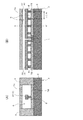
本実施形態では、半導体装置は、図1に示すように、例えばミリ波やテラヘルツ波などの高周波又は超高周波で高速動作する半導体素子として増幅素子(トランジスタ素子)1を備える半導体チップ(例えばMMICチップ)2である。そして、この半導体チップ2は、例えば筐体に収納されてモジュール(高周波モジュール)とされ、増幅器(半導体増幅器)として、通信装置に搭載される。
Hereinafter, a semiconductor device, a manufacturing method thereof, and a communication device according to embodiments of the present invention will be described with reference to FIGS.
The semiconductor device according to the present embodiment is a semiconductor device including a semiconductor element that operates at a high frequency or an ultrahigh frequency and is provided in a communication device such as a transmitter, a receiver, and a transceiver.
In the present embodiment, as shown in FIG. 1, the semiconductor device includes a semiconductor chip (for example, an MMIC chip) including an amplifying element (transistor element) 1 as a semiconductor element that operates at a high frequency such as a millimeter wave or a terahertz wave or a high frequency. ) 2. The
ここでは、例えばミリ波やテラヘルツ波などの高周波又は超高周波で高速動作する増幅素子1として、例えばInP−HEMTを用いる。
例えば、InP−HEMT1は、InP基板3[ここでは半絶縁性InP基板(SI−InP基板);半導体基板]上に、InGaAs電子走行層(チャネル層)及びInAlAs電子供給層を含む半導体積層構造(HEMT構造)を設け、その上方にソース電極、ドレイン電極、ゲート電極を設けた構造になっている。なお、表面保護膜として絶縁膜(例えばSiN膜)が設けられている場合もある。このInP−HEMT1は、高い周波数で低雑音であり、かつ、高い電力増幅率を持つという特徴である。
Here, for example, InP-HEMT is used as the amplifying element 1 that operates at high speed such as millimeter wave or terahertz wave at high frequency or ultra high frequency.
For example, the InP-HEMT 1 has a semiconductor stacked structure (including a InGaAs electron transit layer (channel layer) and an InAlAs electron supply layer on an InP substrate 3 [here, a semi-insulating InP substrate (SI-InP substrate); a semiconductor substrate) ( (HEMT structure) is provided, and a source electrode, a drain electrode, and a gate electrode are provided thereabove. Note that an insulating film (for example, a SiN film) may be provided as a surface protective film. This InP-HEMT1 is characterized by low noise at a high frequency and high power gain.
そして、本半導体チップ2では、半導体素子1としてInP−HEMTが設けられた半導体基板3の上方に、InP−HEMT1に接続された信号配線4(例えばAuからなる)が設けられている。この信号配線4は、例えばミリ波やテラヘルツ波などの高周波又は超高周波で動作する半導体素子1に接続され、高周波又は超高周波の信号を伝送するための配線である。
In the
ここでは、信号配線4として、InP−HEMT1の入力側、即ち、InP−HEMT1のゲート電極に入力側の信号配線(入力配線)4Xが接続されており、InP−HEMT1の出力側、即ち、InP−HEMT1のドレイン電極に出力側の信号配線(出力配線)4Yが接続されている。つまり、ここでは、信号配線4として、入力配線4Xと出力配線4Yの2つの信号配線が接続されている。なお、InP−HEMT1のソース電極はグランドに接続されている。
Here, as the
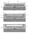
また、ここでは、信号配線4のInP−HEMT1に接続されている側の反対側の端部は、端子5(コンタクト端子)に接続されている(図2(A)、図2(B)参照)。つまり、入力配線4XのInP−HEMT1に接続されている側の反対側の端部は、端子(入力端子)5Xに接続されており、出力配線4YのInP−HEMT1に接続されている側の反対側の端部は、端子(出力端子)5Yに接続されている。
Here, the end of the
また、本半導体チップ2では、信号配線4の上方及び下方のそれぞれに空間(空洞)6を挟んで設けられた上部金属層7A及び下部金属層7Bを備える。
ここでは、下部金属層7Bは、半導体基板3としてのInP基板上に、信号配線4としての入力配線4X及び出力配線4Yが延びる方向に沿って延びるように設けられている。また、上部金属層7Aは、信号配線4を挟んで下部金属層7Bの反対側に設けられており、下部金属層7Bが設けられている領域に対応して、信号配線4としての入力配線4X及び出力配線4Yが延びる方向に沿って延びるように設けられている。これらの上部金属層7A及び下部金属層7Bは、グランドに接続されているため、グランド層であり、また、信号配線4をシールドしているため、シールド層でもある。このため、上部金属層7A及び下部金属層7Bを、金属グランド層、金属シールド層又は金属グランド・シールド層ともいう。ここでは、これらの上部金属層7A及び下部金属層7Bは、例えばAuからなる。
The
Here, the
このように、信号配線4の上方及び下方のそれぞれに空間6を挟んで上部金属層7A及び下部金属層7Bが設けられているため、信号配線4における伝送損失を低減し、伝送特性を向上させることができる。
つまり、信号配線4の上方及び下方の両方に金属グランド層7A,7Bが設けられていることになるため、実質的な電流が増加し、特に高周波又は超高周波の信号は通りやすくなるため、伝送損失を低減することができる。
Thus, since the
That is, since the metal ground layers 7A and 7B are provided both above and below the
また、信号配線4と上方及び下方の両方の金属グランド層7A,7Bとの間が空間6になっているため、絶縁層が介在する場合(例えば図17(A)、図17(B)参照)と比較して、高いインピーダンスを実現することができ、伝送損失(例えば絶縁層による信号のロス)を低減することができる。これに対し、従来のコプレーナー型(例えば図17(A)参照)やマイクロストリップ型(例えば図17(B)参照)の配線ではグランド層との間に絶縁層が介在することになるため、低インピーダンスになり、寄生抵抗成分の影響を受け易く、伝送損失が大きくなってしまう。
Further, since the
また、信号配線4の上方が金属シールド層7Aによってシールドされているため、外部からのノイズの影響を抑えることができ、伝送特性を向上させることができる。例えば、テラヘルツ帯のような超高周波領域になると、外部からのノイズの影響を受けやすくなるが、このような外部からのノイズの影響を抑えることができ、伝送特性を向上させることができる。
In addition, since the upper part of the
また、信号配線4の下方が金属シールド層7Bによってシールドされているため、半導体基板3を介した信号のフィードバックの影響を抑えることができ、伝送特性を向上させることができる。例えば、テラヘルツ帯のような超高周波領域になると、半導体基板3を介した余分なフィードバック電磁波が信号配線4に伝わることになり、伝送特性に影響を及ぼすことになるが、このようなフィードバックの影響を抑え、動作を安定化することができ、伝送特性を向上させることができる。
In addition, since the lower part of the
そして、信号配線4は、信号配線4と下部金属層7Bとの間に設けられた絶縁体8によって支持されている。つまり、上部金属層7Aと下部金属層7Bとの間の空間6内に設けられた信号配線4としての入力配線4X及び出力配線4Yが、下部金属層7B上に絶縁体8を介して支持されて、空間6内に固定されている。これにより、信号配線4の機械的強度を保ち、信号配線4の変形を抑制することができる。また、信号配線4の形状の変形を抑制することができるため、信号配線4と上部金属層7A及び下部金属層7Bとの間の距離を一定に保つことができ、信号配線4の変形によるインピーダンスの変化を抑制し、信号のロスが増大してしまうのを抑制することができる。これに対し、例えばエアブリッジ配線(例えば図17(C)参照)のように配線が支持されていないと、機械的強度が弱く、配線が変形してしまい、この結果、インピーダンスが変化して、信号のロスが増大してしまうことになる。なお、このように絶縁体8によって支持される信号配線4を備えるため、これを支持配線型半導体装置ともいう。
The
本実施形態では、絶縁体8は、柱状(支柱状)になっており、信号配線4が延びる方向に沿って間隔をあけて複数設けられている。これにより、信号配線4に接触する面積を減らすことができ、より伝送損失を低減することができる。この場合、複数の柱状の絶縁体8の間隔は、信号配線が落ちたり、歪んだりしないように、適度な間隔に保つことで、信号配線4の変形を抑制し、形状の安定化を図ることができる。また、複数の柱状の絶縁体8の間隔は、使用する周波数(使用する信号波長)に基づいて設定すれば良く、信号波長の1/4以上になるようにするのが好ましい。これにより、絶縁体8によって支持することによる伝送損失への影響を抑制することができ、さらに伝送損失を低減することができる。特に、テラヘルツ帯などの超高周波での伝送損失を低減するのに効果的である。ここでは、絶縁体8は、低誘電率材料からなる低誘電体であり、例えばベンゾシクロブテン(BCB)樹脂からなる低誘電率の絶縁体である。なお、絶縁体8の材料は、BCB樹脂に限られるものではなく、例えばSOGなどの他の低誘電率材料を用いても良く、コーティングして硬化させることができるものであることが好ましい。
In this embodiment, the
なお、このように、少なくとも上部金属層7A及び下部金属層7Bが設けられていれば良いが、例えば図2(C)に示すように、信号配線4の側方に空間6を挟んで側部金属層7Cが設けられているのが好ましい。つまり、上部金属層7A及び下部金属層7Bの両側部を連結するように側部金属層7Cが設けられているのが好ましい。ここでは、側部金属層7Cも例えばAuからなる。このように、信号配線4の全周囲を取り囲むように金属層7A〜7Cが設けられているのが好ましい。この場合、信号配線4の全周囲が、例えばAuからなる金属層7A〜7Cで覆われ、シールドされることになる。
As described above, at least the
また、例えば図2(A)、図2(B)に示すように、端子5(コンタクト端子)及び信号配線4の端子5に接続されている部分(信号配線の引き出し部分)を取り囲むように端部金属層7Dが設けられているのが好ましい。つまり、上部金属層7A及び下部金属層7Bに連なり、端子5及び信号配線4の端子5に接続されている部分の全周囲を取り囲むように、端部金属層7Dが設けられているのが好ましい。ここでは、入力端子5Xが設けられている側に、入力端子5X及び入力配線4Xの入力端子5Xに接続されている部分を取り囲むように入力側端部金属層7DXが設けられており、出力端子5Yが設けられている側に、出力端子5Y及び出力配線4Yの出力端子5Yに接続されている部分を取り囲むように出力側端部金属層7DYが設けられているのが好ましい。この場合、端子5を含む信号配線4の全体が金属層7A〜7Dで覆われ、シールドされることになる。これにより、半導体基板3からの信号の回り込みを抑制することができ、伝送特性を向上させることが可能となる。
Further, for example, as shown in FIG. 2A and FIG. 2B, the terminal 5 (contact terminal) and the end of the
そして、絶縁体8で支持された信号配線4に対して空間6を挟んで設けられたシールドの外部には、絶縁層9が設けられている。つまり、半導体基板3の上方の信号配線4、上部金属層7A、下部金属層7B、絶縁体8及び空間6(ここではさらに側部金属層7C及び端部金属層7Dを含む)が設けられている領域の外側は絶縁層9で埋め込まれている。このように、本半導体チップ2は、上述のように構成される配線構造が、絶縁層9によって、半導体素子1が設けられている半導体基板3上に一体化された構成になっている。ここでは、絶縁層9は、例えばBCB樹脂からなる絶縁層である。なお、絶縁層9の材料は、BCB樹脂に限られるものではなく、例えばSOGなどの他の低誘電率材料を用いても良く、コーティングして硬化させることができるものであることが好ましい。
An insulating
なお、上述のようにして、半導体基板3の上方に設けられた配線構造の上に、同様の構造を有する配線構造を積層させて、多層構造の配線構造としても良い。また、同一半導体基板3上に、複数の半導体素子1が設けられており、これらの複数の半導体素子1のそれぞれに上述のような配線構造が設けられていても良い。
次に、本実施形態にかかる半導体装置の製造方法について説明する。
As described above, a wiring structure having a similar structure may be laminated on the wiring structure provided above the
Next, a method for manufacturing the semiconductor device according to the present embodiment will be described.
本半導体装置の製造方法は、半導体素子が設けられた半導体基板の上方に、下部金属層を形成する工程と、下部金属層上に、絶縁体及び絶縁体の周囲の下部犠牲層を形成する工程と、絶縁体上に、半導体素子に接続され、かつ、絶縁体に支持されるように、信号配線を形成する工程と、信号配線を覆うように上部犠牲層を形成する工程と、上部犠牲層上に、上部金属層を形成する工程と、下部犠牲層及び上部犠牲層を除去して、信号配線と下部金属層との間及び信号配線と上部金属層との間に空間を形成する工程と、半導体基板の上方の信号配線、上部金属層、下部金属層、絶縁体及び空間が設けられている領域の外側を埋め込む絶縁層を形成する工程とを含む。 The method for manufacturing a semiconductor device includes a step of forming a lower metal layer above a semiconductor substrate provided with a semiconductor element, and a step of forming an insulator and a lower sacrificial layer around the insulator on the lower metal layer. A step of forming a signal wiring on the insulator so as to be connected to the semiconductor element and supported by the insulator; a step of forming an upper sacrificial layer so as to cover the signal wiring; and an upper sacrificial layer Forming an upper metal layer; removing the lower sacrificial layer and the upper sacrificial layer; forming a space between the signal wiring and the lower metal layer and between the signal wiring and the upper metal layer; And forming a signal wiring above the semiconductor substrate, an upper metal layer, a lower metal layer, an insulator, and an insulating layer filling the outside of the region where the space is provided.
以下、図3〜図6を参照しながら、具体例を挙げて説明する。
なお、ここでは、図2に示す構造のものを製造する場合を例に挙げて説明する。
まず、図3(A)に示すように、半導体基板3上に半導体素子1を設ける。
ここでは、InP基板3上に、InGaAs電子走行層(チャネル層)及びInAlAs電子供給層を含む半導体積層構造を備え、その上方にソース電極、ドレイン電極、ゲート電極を備えるInP−HEMT1を形成する。
Hereinafter, a specific example will be described with reference to FIGS.
Here, the case of manufacturing the structure shown in FIG. 2 will be described as an example.
First, as shown in FIG. 3A, the semiconductor element 1 is provided over the
Here, an InP-HEMT 1 having a semiconductor stacked structure including an InGaAs electron transit layer (channel layer) and an InAlAs electron supply layer on an
具体的には、半絶縁性InP基板3上に、i−InAlAsバッファ層(厚さ約300nm)、i−InGaAsチャネル層(厚さ約15nm)、i−InAlAsスペーサ層(厚さ約3nm)、δドープ層(ドーピング濃度約2×1012cm−2)及びi−InAlAsバリア層(厚さ約8nm)からなる電子供給層、n−InGaAsキャップ層(厚さ約50nm)を、それぞれ、結晶成長させ、例えばフォトリソグラフィなどを用いて、その上方にソース電極、ドレイン電極、ゲート電極を形成して、InP−HEMT1を形成する。
Specifically, on the
次に、図3(B)に示すように、半導体素子1が設けられた半導体基板3の上方に、下部金属層7Bを形成する。
ここでは、InP−HEMT1が設けられたInP基板3の上方に、InP−HEMT1を取り囲むように、グランド層及びシールドとなる下部金属層7Bとして、Au層を形成する。具体的には、例えばTi(厚さ約10nm)/Pt(厚さ約30nm)/Au(厚さ約300nm)を蒸着し、リフトオフ法によって、下部金属層7Bを形成する。この場合、Ti層は密着層であり、Pt層はバリア層である。
Next, as shown in FIG. 3B, a
Here, an Au layer is formed as a
次に、図3(C)、図3(D)に示すように、下部金属層7B上に、絶縁体8及び絶縁体8の周囲の下部犠牲層10を形成する。
ここでは、まず、図3(C)に示すように、下部金属層7B上に、信号配線4を支持する柱状の絶縁体8を、間隔をあけて、複数形成する。具体的には、全面にBCB樹脂を塗布し、約250℃以上の温度でキュアすることで硬化させ、フォトリソグラフィを用いてマスクを形成し、酸素を含んだドライエッチングによってBCB樹脂をエッチングして、柱状のBCB樹脂からなる絶縁体8を、間隔をあけて、複数形成する。
Next, as shown in FIGS. 3C and 3D, the
Here, first, as shown in FIG. 3C, a plurality of
次に、図3(D)に示すように、下部金属層7B上に、絶縁体8の周囲が埋め込まれるように下部犠牲層10を形成する。具体的には、全面にPMGI(poly(dimethylglutarimide))樹脂を塗布し、約250℃以上の温度でキュアすることで硬化させ、酸素系のドライエッチングでエッチバックを行なって平坦化して、PMGI樹脂からなる下部犠牲層10を形成する。
Next, as shown in FIG. 3D, a lower
なお、このような方法に限られるものではなく、例えば、図6(A)に示すように、全面にPMGI樹脂100を塗布し、約250℃以上の温度でキュアすることで硬化させ、フォトリソグラフィを用いてマスクを形成し、図6(B)に示すように、酸素を含んだドライエッチングによってPMGI樹脂100をエッチングして絶縁体8を設ける開口部100Xを形成し、図6(C)に示すように、全面にBCB樹脂80を塗布して開口部100XにBCB樹脂80を充填し、約250℃以上の温度でキュアすることで硬化させ、図6(D)に示すように、BCB樹脂80のエッチバックを行なって、開口部100Xに充填されたBCB樹脂80を露出させることで、下部金属層7B上に、BCB樹脂80からなる絶縁体8及び絶縁体8の周囲にPMGI樹脂100からなる下部犠牲層10を形成しても良い。
Note that the present invention is not limited to such a method. For example, as shown in FIG. 6A,
次に、フォトリソグラフィを用いてコンタクトホールを形成する領域に開口部を有するマスクを形成し、図4(A)に示すように、InP−HEMT1のゲート電極及びドレイン電極上に設けられているPMGI樹脂からなる下部犠牲層10をドライエッチングしてコンタクトホール11を形成する。
次に、図4(B)に示すように、絶縁体8上に、半導体素子1としてのInP−HEMTに接続され、かつ、絶縁体8に支持されるように、信号配線4(ここでは入力配線4X及び出力配線4Y)を形成する。
Next, a mask having an opening is formed in a region where a contact hole is to be formed using photolithography, and the PMGI provided over the gate electrode and the drain electrode of the InP-HEMT 1 as illustrated in FIG. The lower
Next, as shown in FIG. 4B, the signal wiring 4 (here, input) is connected to the InP-HEMT as the semiconductor element 1 and supported by the
ここでは、BCB樹脂からなる複数の柱状の絶縁体8及びPMGI樹脂からなる下部犠牲層10上に、フォトリソグラフィを用いて信号配線4を形成する領域に開口部を有するマスクを形成し、金めっきによって、信号配線4を形成する。この場合、コンタクトホール11も金めっきによって埋め込まれる。これにより、InP−HEMT1のゲート電極及びドレイン電極に接続され、BCB樹脂からなる複数の柱状の絶縁体8によって支持されるように、Auからなる信号配線4が形成される。
Here, on the plurality of
次に、図4(C)に示すように、信号配線4を覆うように上部犠牲層12を形成する。具体的には、全面にPMGI樹脂を塗布し、約250℃以上の温度でキュアすることで硬化させ、上部犠牲層12を形成する。
次に、フォトリソグラフィを用いて端子5と信号配線4とを接続する部分、側部金属層7C及び端部金属層7Dを形成する領域に開口部を有するマスクを形成し、図5(A)に示すように、上部犠牲層12及び下部犠牲層10としてのPMGI樹脂をドライエッチングする。
Next, as shown in FIG. 4C, the upper
Next, a mask having an opening is formed in a portion where the
次に、フォトリソグラフィを用いて端子5、側部金属層7C、端部金属層7D及び上部金属層7Aを形成する領域に開口部を有するマスクを形成し、図5(B)に示すように、金めっきを行なって、端子5(ここでは入力端子5X及び出力端子5Y)、側部金属層7C(図示せず)、端部金属層7D及び上部金属層7Aを形成する。この工程は、上部犠牲層12上に上部金属層7Aを形成する工程である。
Next, a mask having an opening is formed in a region where the
次に、図5(C)に示すように、下部犠牲層10及び上部犠牲層12を除去して、信号配線4と下部金属層7Bとの間及び信号配線4と上部金属層7Aとの間に空間6を形成する。具体的には、溶剤によって下部犠牲層10及び上部犠牲層12を構成するPMGI樹脂を溶解させることによって、信号配線4の周囲に空間6を形成する。この場合、空間6内に設けられた信号配線4はBCB樹脂からなる複数の柱状の絶縁体8によって支持されて固定されることになる。
Next, as shown in FIG. 5C, the lower
次に、半導体基板1の上方の信号配線4、上部金属層7A、下部金属層7B、絶縁体8及び空間6(ここでは側部金属層7C及び端部金属層7Dも含む)が設けられている領域の外側を埋め込む絶縁層9を形成する(例えば図2参照)。ここでは、InP基板3上の配線構造が設けられている領域の外側をBCB樹脂からなる絶縁層9で埋め込む。
このようにして、本実施形態の半導体装置(半導体チップ)2を製造することができる。
Next, the
In this way, the semiconductor device (semiconductor chip) 2 of this embodiment can be manufactured.
したがって、本実施形態にかかる半導体装置及びその製造方法、通信装置によれば、高周波又は超高周波で高速動作する半導体素子1を備える半導体装置2に備えられる配線4における伝送損失を低減し、伝送特性を向上させることができるという利点がある。
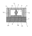
なお、上述の実施形態の構成に限られるものではなく、例えば図7に示すように、さらに、信号配線4と上部金属層7Aとの間に設けられ、上部金属層7Aを支持する金属層支持用絶縁体13を備えるものとしても良い。この場合、金属層支持用絶縁体13は柱状になっているものとすれば良い。なお、上述の実施形態(図1参照)のように側部金属層7Cが設けられていなくても良い。
Therefore, according to the semiconductor device, the manufacturing method thereof, and the communication device according to the present embodiment, the transmission loss in the
The configuration is not limited to the above-described embodiment. For example, as shown in FIG. 7, a metal layer support that is provided between the
また、この場合、半導体装置の製造方法は、上部金属層7Aを支持する金属層支持用絶縁体13を形成する工程を含むことになる。例えば、信号配線4を形成した後、上部犠牲層12を形成する前に、図8(A)に示すように、信号配線4上に、上部金属層7Aを支持する柱状の金属層支持用絶縁体13を、間隔をあけて、複数形成する工程を含むものとし、上部犠牲層12を形成する工程で、図8(B)に示すように、複数の柱状の金属層支持用絶縁体13の周囲が埋め込まれるように上部犠牲層12を形成すれば良い。具体的には、全面にBCB樹脂を塗布し、約250℃以上の温度でキュアすることで硬化させ、フォトリソグラフィを用いてマスクを形成し、酸素を含んだドライエッチングによってBCB樹脂をエッチングして、図8(A)に示すように、信号配線4としてのAu配線上に、柱状のBCB樹脂からなる金属層支持用絶縁体13を、間隔をあけて、複数形成し、次いで、図8(B)に示すように、全面にPMGI樹脂を塗布し、約250℃以上の温度でキュアすることで硬化させ、酸素系のドライエッチングでエッチバックを行なって平坦化して、上部犠牲層12を形成すれば良い。
In this case, the method for manufacturing a semiconductor device includes a step of forming the metal
また、この場合、信号配線4は上方からも支持されることになるため、より確実に、その機械的強度を保ち、信号配線4の変形(歪み)を抑制することが可能となる。このように、信号配線4の機械的強度を保ち、信号配線4の変形を抑制するためには、上下方向の両方向から支持するのが有効である。また、この場合、金属層支持用絶縁体13を設けることで、上部金属層7Aの変形を抑制することができ、ひいては、信号配線4の周囲の空間の形状が変わってしまうのを抑制することができる。これにより、信号配線4と上部金属層7A及び下部金属層7Bとの間の距離を一定に保つことができ、信号配線4や上部金属層7Aの変形によるインピーダンスの変化を抑制し、信号のロスが増大してしまうのを抑制することができる。
In this case, since the
また、例えば図9に示すように、下部金属層7Bと上部金属層7Aとの間に設けられ、上部金属層7Aを支持する金属層支持用絶縁体14を備えるものとしても良い。この場合、金属層支持用絶縁体14は柱状になっているものとすれば良い。なお、上述の実施形態(図1参照)のように側部金属層7Cが設けられていなくても良い。また、信号配線4と上部金属層7Aとの間に設けられた金属層支持用絶縁体13を備えないものとしても良い。
For example, as shown in FIG. 9, a metal
また、この場合、半導体装置の製造方法は、上部金属層7Aを支持する金属層支持用絶縁体14を形成する工程を含むことになる。例えば、上部犠牲層12を形成した後、上部金属層7Aを形成する前に、下部金属層7B上に、上部金属層7Aを支持する柱状の金属層支持用絶縁体14を、間隔をあけて、複数形成する工程を含むものとすれば良い。具体的には、フォトリソグラフィを用いてマスクを形成し、酸素を含んだドライエッチングによってPMGI樹脂からなる上部犠牲層12をエッチングして金属層支持用絶縁体14を設ける穴を形成し、全面にBCB樹脂を塗布して穴にBCB樹脂を充填し、約250℃以上の温度でキュアすることで硬化させ、BCB樹脂のエッチバックを行なって、穴に充填されたBCB樹脂を露出させることで、下部金属層7B上に、柱状のBCB樹脂からなる金属層支持用絶縁体14を、間隔をあけて、複数形成すれば良い。
In this case, the method for manufacturing a semiconductor device includes a step of forming the metal
また、この場合、金属層支持用絶縁体14を設けることで、上部金属層7Aの変形を抑制することができ、ひいては、信号配線4の周囲の空間の形状が変わってしまうのを抑制することができる。これにより、信号配線4と上部金属層7A及び下部金属層7Bとの間の距離を一定に保つことができ、信号配線4や上部金属層7Aの変形によるインピーダンスの変化を抑制し、信号のロスが増大してしまうのを抑制することができる。
Further, in this case, by providing the metal
また、上述の実施形態では、信号配線4を支持する絶縁体8は、柱状になっているが、これに限られるものではない。
例えば図10に示すように、信号配線4を支持する絶縁体8Aは、板状になっており、信号配線4が延びる方向に交差する方向に延びるように設けられており、さらに、この絶縁体8A及び信号配線4と上部金属層7Aとの間に設けられ、上部金属層7Aを支持する金属層支持用絶縁体14Aを備えるものとしても良い。ここでは、金属層支持用絶縁体14Aも板状になっている。また、絶縁体8Aと金属層支持用絶縁体14Aは一体化されており、一枚の板状になっている。なお、上述の実施形態(図1参照)のように側部金属層7Cが設けられていなくても良い。
In the above-described embodiment, the
For example, as shown in FIG. 10, the
この場合、信号配線4は上下左右から支持されることになるため、より確実に、その機械的強度を保ち、信号配線4の変形を抑制することが可能となる。このように、信号配線4の機械的強度を保ち、信号配線4の変形を抑制するためには、上下左右方向の複数の方向から支持するのが有効である。また、この場合、金属層支持用絶縁体14Aを設けることで、上部金属層7Aの変形を抑制することができ、ひいては、信号配線4の周囲の空間の形状が変わってしまうのを抑制することができる。これにより、信号配線4と上部金属層7A及び下部金属層7Bとの間の距離を一定に保つことができ、信号配線4や上部金属層7Aの変形によるインピーダンスの変化を抑制し、信号のロスが増大してしまうのを抑制することができる。
In this case, since the
また、この場合、半導体装置の製造方法は、絶縁体を形成する工程において、信号配線4が延びる方向に交差する方向に延びるように板状の絶縁体8Aを形成するようにし、さらに、上部金属層7Aを支持する金属層支持用絶縁体14Aを形成する工程を含むことになる。この金属層支持用絶縁体14Aを形成する工程においても、絶縁体8A及び信号配線4の上に、板状の金属層支持用絶縁体14Aを形成することになる。なお、ここでは、絶縁体8Aと金属層支持用絶縁体14Aが1枚の板状になっており、これによって空間6が仕切られることになるため、溶剤によって犠牲層を溶解させて空間6を形成する際に溶剤を入れ、犠牲層を除去するための開口部15を形成することになる(例えば図10(A)参照)。
In this case, in the method of manufacturing the semiconductor device, in the step of forming the insulator, the plate-
また、例えば図11に示すように、信号配線4を支持する絶縁体8Bは、信号配線4を支持する平面状部分8BXと、平面状部分8BXの両側部と下部金属層7Bとの間に設けられ、平面状部分8BXを支持する支持部分8BYとを備えるものとしても良い。なお、半導体装置の製造方法において、下部犠牲層10を覆うようにBCB樹脂を設け、その上に信号配線4を形成することで、信号配線4を支持する平面状部分8BXを形成することができ、支持部分8BYは、上述の実施形態のBCB樹脂からなる柱状の絶縁体8と同様にして形成することができる。なお、上述の実施形態(図1参照)のように側部金属層7Cが設けられていなくても良い。
For example, as shown in FIG. 11, the
この場合、信号配線4を支持する絶縁体8Bは、さらに、板状になっており、平面状部分8BXと下部金属層7Bとの間に信号配線4が延びる方向に交差する方向に延びるように設けられ、平面状部分8BXを支持しており、信号配線4が延びる方向に沿って間隔をあけて複数設けられている板状支持部分8BZを備えるものとしても良い。この場合、複数の板状支持部分8BZの間隔は、信号波長の1/4以上になっているのが好ましい。なお、半導体装置の製造方法において、板状支持部分8BZは、上述の変形例のBCB樹脂からなる板状の絶縁体8Aと同様にして形成することができる。なお、この板状支持部分8BZを備えないものとしても良い。また、上述の実施形態(図1参照)のように側部金属層7Cが設けられていなくても良い。
In this case, the
また、例えば図12に示すように、上部金属層7Aを支持する金属層支持用平面状部分14BXと、金属層支持用平面状部分14BXの両側部と平面状部分8BXの両側部との間に設けられ、金属層支持用平面状部分14BXを支持する金属層支持用支持部分14BYとを備える金属層支持用絶縁体14Bを備えるものとしても良い。この場合、半導体装置の製造方法は、上部金属層7Aを支持する金属層支持用絶縁体14Bを形成する工程を含むことになる。なお、半導体装置の製造方法において、上部犠牲層12を覆うようにBCB樹脂を設け、その上に上部金属層7Aを形成することで、上部金属層7Aを支持する金属層支持用平面状部分14BXを形成することができ、金属層支持用支持部分14BYは、上述の変形例のBCB樹脂からなる柱状の金属層支持用絶縁体13と同様にして形成することができる。なお、上述の実施形態(図1参照)のように側部金属層7Cが設けられていなくても良い。
Further, for example, as shown in FIG. 12, the metal layer supporting planar portion 14BX that supports the
この場合、金属層支持用絶縁体14Bは、さらに、板状になっており、平面状部分8BX及び信号配線4と金属層支持用平面状部分14BXとの間に信号配線4が延びる方向に交差する方向に延びるように設けられ、金属層支持用平面状部分14BXを支持しており、信号配線4が延びる方向に沿って間隔をあけて複数設けられている金属層支持用板状支持部分14BZを備えるものとしても良い。この場合、複数の金属層支持用板状支持部分14BZの間隔は、信号波長の1/4以上になっているのが好ましい。また、この場合、半導体装置の製造方法は、上部金属層7Aを支持する金属層支持用絶縁体14Bを形成する工程を含むことになる。なお、半導体装置の製造方法において、金属層支持用板状支持部分14BZは、上述の変形例の板状の金属層支持用絶縁体14Aと同様にして形成することができる。なお、この金属層支持用板状支持部分14BZを備えないものとしても良い。また、上述の実施形態(図1参照)のように側部金属層7Cが設けられていなくても良い。
In this case, the metal
また、上述の実施形態の構成に限られるものではなく、例えば図13に示すように、空間6に設けられた他の信号配線20と、他の信号配線20を支持する他の絶縁体21とを備えるものとしても良い。この場合、他の信号配線20と上部金属層7Aとの間に上部金属層7Aを支持する金属層支持用絶縁体22を設けても良い。このようにして多層配線構造としても良い。なお、金属層支持用絶縁体22は設けなくても良い。なお、上述の実施形態(図1参照)のように側部金属層7Cが設けられていなくても良い。
Further, the configuration is not limited to the above-described embodiment. For example, as illustrated in FIG. 13, another
また、上述の実施形態の構成に限られるものではなく、例えば図14に示すように、信号配線4と絶縁体8との間に絶縁体8と異なる絶縁材料からなる絶縁膜23を備えるものとしても良い。例えば、上述の実施形態のように、信号配線4を支持する絶縁体8をBCB樹脂とする場合、信号配線4の直下、即ち、信号配線4とBCB樹脂からなる絶縁体8との間に、例えばSiN膜などのCVD法(プラズマCVD法)などによって成膜できる絶縁膜23を備えるものとしても良い。これにより、信号配線4を形成しやすくなる。なお、上述の実施形態(図1参照)のように側部金属層7Cが設けられていなくても良い。また、ここでは、金属層支持用絶縁体13を設けているが、これを備えないものとしても良い。
Further, the configuration is not limited to the above-described embodiment. For example, as shown in FIG. 14, an insulating
また、上述の実施形態の構成に限られるものではなく、例えば図15に示すように、信号配線4の表面、上部金属層7A及び下部金属層7Bの内側表面を覆う保護絶縁膜24を備えるものとしても良い。ここでは、側部金属層7Cも備えられており、この内側表面も保護絶縁膜24によって覆われるようにしている。これにより、信号配線4や金属層7A〜7Cの表面を保護することができる。なお、端部金属層7Dの内側表面も保護絶縁膜24に覆われるようにしても良い。また、保護絶縁膜24は、金属表面を保護できれば良いため、厚さが薄い絶縁膜である。なお、上述の実施形態(図1参照)のように側部金属層7Cが設けられていなくても良い。また、ここでは、金属層支持用絶縁体13を設けているが、これを備えないものとしても良い。
Further, the present invention is not limited to the configuration of the above-described embodiment. For example, as shown in FIG. 15, a protective insulating
また、上述の実施形態の構成に限られるものではなく、例えば図16に示すように、下部金属層7Bとしてのグランド層と側部金属層7Cとの間にスリット25が入っている構造であっても良い。なお、ここでは、金属層支持用絶縁体13を設けているが、これを備えないものとしても良い。
また、上述の実施形態では、半導体素子1をInP−HEMTとしているが、これに限られるものではなく、例えばInP−HBT、GaN−HEMT、Si基板上に設けられるCMOSなどであっても良いし、また、ショットキーダイオード、トンネルダイオードなどの2端子デバイス(整流素子)であっても良い。
Further, the present invention is not limited to the configuration of the above-described embodiment. For example, as shown in FIG. 16, the
In the above-described embodiment, the semiconductor element 1 is InP-HEMT. However, the invention is not limited to this. For example, the semiconductor element 1 may be InP-HBT, GaN-HEMT, CMOS provided on a Si substrate, or the like. Also, a two-terminal device (rectifier element) such as a Schottky diode or a tunnel diode may be used.
なお、本発明は、上述した実施形態及び変形例に記載した構成に限定されるものではなく、本発明の趣旨を逸脱しない範囲で種々変形することが可能である。
以下、上述の実施形態及び変形例に関し、更に、付記を開示する。
(付記1)
半導体基板上に設けられた半導体素子と、
前記半導体基板の上方に設けられ、前記半導体素子に接続された信号配線と、
前記信号配線の上方及び下方のそれぞれに空間を挟んで設けられた上部金属層及び下部金属層と、
前記信号配線と前記下部金属層との間に設けられ、前記信号配線を支持する絶縁体と、
前記半導体基板の上方の前記信号配線、前記上部金属層、前記下部金属層、前記絶縁体及び前記空間が設けられている領域の外側を埋め込む絶縁層とを備えることを特徴とする半導体装置。
Note that the present invention is not limited to the configurations described in the above-described embodiments and modifications, and various modifications can be made without departing from the spirit of the present invention.
Hereinafter, additional notes will be disclosed regarding the above-described embodiment and modifications.
(Appendix 1)
A semiconductor element provided on a semiconductor substrate;
A signal wiring provided above the semiconductor substrate and connected to the semiconductor element;
An upper metal layer and a lower metal layer provided with a space above and below the signal wiring, respectively,
An insulator provided between the signal wiring and the lower metal layer and supporting the signal wiring;
A semiconductor device comprising: the signal wiring above the semiconductor substrate, the upper metal layer, the lower metal layer, the insulator, and an insulating layer that fills the outside of the region where the space is provided.
(付記2)
前記信号配線の側方に空間を挟んで設けられた側部金属層を備えることを特徴とする、付記1に記載の半導体装置。
(付記3)
前記絶縁体は、前記信号配線が延びる方向に沿って間隔をあけて複数設けられていることを特徴とする、付記1又は2に記載の半導体装置。
(Appendix 2)
The semiconductor device according to appendix 1, further comprising a side metal layer provided on a side of the signal wiring with a space in between.
(Appendix 3)
The semiconductor device according to
(付記4)
前記絶縁体は、柱状になっていることを特徴とする、付記3に記載の半導体装置。
(付記5)
前記信号配線と前記上部金属層との間に設けられ、前記上部金属層を支持する金属層支持用絶縁体を備えることを特徴とする、付記1〜4のいずれか1項に記載の半導体装置。
(Appendix 4)
4. The semiconductor device according to
(Appendix 5)
The semiconductor device according to any one of appendices 1 to 4, further comprising a metal layer supporting insulator provided between the signal wiring and the upper metal layer and supporting the upper metal layer. .
(付記6)
前記下部金属層と前記上部金属層との間に設けられ、前記上部金属層を支持する金属層支持用絶縁体を備えることを特徴とする、付記1〜5のいずれか1項に記載の半導体装置。
(付記7)
前記金属層支持用絶縁体は、柱状になっていることを特徴とする、付記5又は6に記載の半導体装置。
(Appendix 6)
The semiconductor according to any one of appendices 1 to 5, further comprising a metal layer supporting insulator provided between the lower metal layer and the upper metal layer and supporting the upper metal layer. apparatus.
(Appendix 7)
The semiconductor device according to
(付記8)
前記絶縁体は、板状になっており、前記信号配線が延びる方向に交差する方向に延びるように設けられ、
前記絶縁体及び前記信号配線と前記上部金属層との間に設けられ、前記上部金属層を支持する金属層支持用絶縁体を備えることを特徴とする、付記3に記載の半導体装置。
(Appendix 8)
The insulator has a plate shape and is provided so as to extend in a direction crossing a direction in which the signal wiring extends,
4. The semiconductor device according to
(付記9)
前記絶縁体は、前記信号配線を支持する平面状部分と、前記平面状部分の両側部と前記下部金属層との間に設けられ、前記平面状部分を支持する支持部分とを備えることを特徴とする、付記1又は2に記載の半導体装置。
(付記10)
前記絶縁体は、さらに、板状になっており、前記平面状部分と前記下部金属層との間に前記信号配線が延びる方向に交差する方向に延びるように設けられ、前記平面状部分を支持しており、前記信号配線が延びる方向に沿って間隔をあけて複数設けられている板状支持部分を備えることを特徴とする、付記9に記載の半導体装置。
(Appendix 9)
The insulator includes a planar portion that supports the signal wiring, and a support portion that is provided between both side portions of the planar portion and the lower metal layer and supports the planar portion. The semiconductor device according to
(Appendix 10)
The insulator further has a plate shape, and is provided between the planar portion and the lower metal layer so as to extend in a direction intersecting with the direction in which the signal wiring extends, and supports the planar portion. The semiconductor device according to
(付記11)
前記上部金属層を支持する金属層支持用平面状部分と、前記金属層支持用平面状部分の両側部と前記平面状部分の両側部との間に設けられ、前記金属層支持用平面状部分を支持する金属層支持用支持部分とを備える金属層支持用絶縁体を備えることを特徴とする、付記9又は10に記載の半導体装置。
(Appendix 11)
The metal layer supporting planar portion for supporting the upper metal layer, the metal layer supporting planar portion provided between the both sides of the planar portion for supporting the metal layer and the both sides of the planar portion. 11. The semiconductor device according to
(付記12)
前記金属層支持用絶縁体は、さらに、板状になっており、前記平面状部分及び前記信号配線と前記金属層支持用平面状部分との間に前記信号配線が延びる方向に交差する方向に延びるように設けられ、前記金属層支持用平面状部分を支持しており、前記信号配線が延びる方向に沿って間隔をあけて複数設けられている金属層支持用板状支持部分を備えることを特徴とする、付記11に記載の半導体装置。
(Appendix 12)
The metal layer supporting insulator further has a plate-like shape in a direction intersecting the direction in which the signal wiring extends between the planar portion and the signal wiring and the planar portion for supporting the metal layer. A plate-like support portion for supporting a metal layer, which is provided so as to extend, supports the planar portion for supporting the metal layer, and is provided in plural along the direction in which the signal wiring extends. 14. The semiconductor device according to
(付記13)
前記信号配線の前記半導体素子に接続されている側の反対側の端部に接続された端子と、
前記端子及び前記信号配線の前記端子に接続されている部分を取り囲むように設けられた端部金属層とを備えることを特徴とする、付記1〜12のいずれか1項に記載の半導体装置。
(Appendix 13)
A terminal connected to an end of the signal wiring opposite to the side connected to the semiconductor element;
The semiconductor device according to any one of appendices 1 to 12, further comprising an end metal layer provided so as to surround a portion of the terminal and the signal wiring connected to the terminal.
(付記14)
前記間隔は、信号波長の1/4以上になっていることを特徴とする、付記3〜8、10、12のいずれか1項に記載の半導体装置。
(付記15)
前記空間に設けられた他の信号配線と、
前記他の信号配線を支持する他の絶縁体とを備えることを特徴とする、付記1〜14のいずれか1項に記載の半導体装置。
(Appendix 14)
13. The semiconductor device according to any one of
(Appendix 15)
Other signal wiring provided in the space;
15. The semiconductor device according to any one of appendices 1 to 14, further comprising another insulator that supports the other signal wiring.
(付記16)
前記信号配線と前記絶縁体との間に前記絶縁体と異なる絶縁材料からなる絶縁膜を備えることを特徴とする、付記1〜15のいずれか1項に記載の半導体装置。
(付記17)
前記信号配線の表面、前記上部金属層及び前記下部金属層の内側表面を覆う保護絶縁膜を備えることを特徴とする、付記1〜16のいずれか1項に記載の半導体装置。
(Appendix 16)
16. The semiconductor device according to any one of appendices 1 to 15, further comprising an insulating film made of an insulating material different from that of the insulator between the signal wiring and the insulator.
(Appendix 17)
17. The semiconductor device according to any one of appendices 1 to 16, further comprising a protective insulating film that covers a surface of the signal wiring, and inner surfaces of the upper metal layer and the lower metal layer.
(付記18)
付記1〜17のいずれか1項に記載の半導体装置を備えることを特徴とする通信装置。
(付記19)
半導体素子が設けられた半導体基板の上方に、下部金属層を形成する工程と、
前記下部金属層上に、絶縁体及び前記絶縁体の周囲の下部犠牲層を形成する工程と、
前記絶縁体上に、前記半導体素子に接続され、かつ、前記絶縁体に支持されるように、信号配線を形成する工程と、
前記信号配線を覆うように上部犠牲層を形成する工程と、
前記上部犠牲層上に、上部金属層を形成する工程と、
前記下部犠牲層及び前記上部犠牲層を除去して、前記信号配線と前記下部金属層との間及び前記信号配線と前記上部金属層との間に空間を形成する工程と、
前記半導体基板の上方の前記信号配線、前記上部金属層、前記下部金属層、前記絶縁体及び前記空間が設けられている領域の外側を埋め込む絶縁層を形成する工程とを含むことを特徴とする半導体装置の製造方法。
(Appendix 18)
A communication apparatus comprising the semiconductor device according to any one of appendices 1 to 17.
(Appendix 19)
Forming a lower metal layer above a semiconductor substrate provided with a semiconductor element;
Forming an insulator and a lower sacrificial layer around the insulator on the lower metal layer;
Forming a signal wiring on the insulator so as to be connected to the semiconductor element and supported by the insulator;
Forming an upper sacrificial layer to cover the signal wiring;
Forming an upper metal layer on the upper sacrificial layer;
Removing the lower sacrificial layer and the upper sacrificial layer to form spaces between the signal wiring and the lower metal layer and between the signal wiring and the upper metal layer;
Forming an insulating layer that fills the outside of the region where the signal wiring, the upper metal layer, the lower metal layer, the insulator, and the space are provided above the semiconductor substrate. A method for manufacturing a semiconductor device.
(付記20)
前記上部金属層を支持する金属層支持用絶縁体を形成する工程を含むことを特徴とする、付記19に記載の半導体装置の製造方法。
(Appendix 20)
20. The method of manufacturing a semiconductor device according to appendix 19, comprising a step of forming a metal layer supporting insulator that supports the upper metal layer.
1 半導体素子(InP−HEMT)
2 半導体装置(半導体チップ)
3 InP基板(半導体基板)
4 信号配線
4X 入力配線
4Y 出力配線
5 端子
5X 入力端子
5Y 出力端子
6 空間
7A 上部金属層
7B 下部金属層
7C 側部金属層
7D 端部金属層
8 絶縁体(柱状の絶縁体)
8A 絶縁体
8B 絶縁体
8BX 平面状部分
8BY 支持部分
8BZ 板状支持部分
9 絶縁層
10 下部犠牲層
100 PMGI樹脂
100X 開口部
11 コンタクトホール
12 上部犠牲層
13 金属層支持用絶縁体
14 金属層支持用絶縁体
14A 金属層支持用絶縁体
14B 金属層支持用絶縁体
14BX 金属層支持用平面状部分
14BY 金属層支持用支持部分
14BZ 金属層支持用板状支持部分
20 他の信号配線
21 他の絶縁体
22 金属層支持用絶縁体
23 絶縁膜
24 保護絶縁膜
25 スリット
1 Semiconductor device (InP-HEMT)
2 Semiconductor devices (semiconductor chips)
3 InP substrate (semiconductor substrate)
4
Claims (16)
前記半導体基板の上方に設けられ、前記半導体素子に接続された信号配線と、
前記信号配線の上方及び下方のそれぞれに空間を挟んで設けられた上部金属層及び下部金属層と、
前記信号配線と前記下部金属層との間に設けられ、前記信号配線を支持する絶縁体と、
前記半導体基板の上方の前記信号配線、前記上部金属層、前記下部金属層、前記絶縁体及び前記空間が設けられている領域の外側を埋め込む絶縁層とを備えることを特徴とする半導体装置。 A semiconductor element provided on a semiconductor substrate;
A signal wiring provided above the semiconductor substrate and connected to the semiconductor element;
An upper metal layer and a lower metal layer provided with a space above and below the signal wiring, respectively,
An insulator provided between the signal wiring and the lower metal layer and supporting the signal wiring;
A semiconductor device comprising: the signal wiring above the semiconductor substrate, the upper metal layer, the lower metal layer, the insulator, and an insulating layer that fills the outside of the region where the space is provided.
前記絶縁体及び前記信号配線と前記上部金属層との間に設けられ、前記上部金属層を支持する金属層支持用絶縁体を備えることを特徴とする、請求項3に記載の半導体装置。 The insulator has a plate shape and is provided so as to extend in a direction crossing a direction in which the signal wiring extends,
4. The semiconductor device according to claim 3, further comprising a metal layer supporting insulator provided between the insulator and the signal wiring and the upper metal layer and supporting the upper metal layer. 5.
前記端子及び前記信号配線の前記端子に接続されている部分を取り囲むように設けられた端部金属層とを備えることを特徴とする、請求項1〜12のいずれか1項に記載の半導体装置。 A terminal connected to an end of the signal wiring opposite to the side connected to the semiconductor element;
The semiconductor device according to claim 1, further comprising an end metal layer provided so as to surround the terminal and a portion of the signal wiring connected to the terminal. .
前記下部金属層上に、絶縁体及び前記絶縁体の周囲の下部犠牲層を形成する工程と、
前記絶縁体上に、前記半導体素子に接続され、かつ、前記絶縁体に支持されるように、信号配線を形成する工程と、
前記信号配線を覆うように上部犠牲層を形成する工程と、
前記上部犠牲層上に、上部金属層を形成する工程と、
前記下部犠牲層及び前記上部犠牲層を除去して、前記信号配線と前記下部金属層との間及び前記信号配線と前記上部金属層との間に空間を形成する工程と、
前記半導体基板の上方の前記信号配線、前記上部金属層、前記下部金属層、前記絶縁体及び前記空間が設けられている領域の外側を埋め込む絶縁層を形成する工程とを含むことを特徴とする半導体装置の製造方法。 Forming a lower metal layer above a semiconductor substrate provided with a semiconductor element;
Forming an insulator and a lower sacrificial layer around the insulator on the lower metal layer;
Forming a signal wiring on the insulator so as to be connected to the semiconductor element and supported by the insulator;
Forming an upper sacrificial layer to cover the signal wiring;
Forming an upper metal layer on the upper sacrificial layer;
Removing the lower sacrificial layer and the upper sacrificial layer to form spaces between the signal wiring and the lower metal layer and between the signal wiring and the upper metal layer;
Forming an insulating layer that fills the outside of the region where the signal wiring, the upper metal layer, the lower metal layer, the insulator, and the space are provided above the semiconductor substrate. A method for manufacturing a semiconductor device.
Priority Applications (1)
| Application Number | Priority Date | Filing Date | Title |
|---|---|---|---|
| JP2016001934A JP6657970B2 (en) | 2016-01-07 | 2016-01-07 | Semiconductor device, manufacturing method thereof, and communication device |
Applications Claiming Priority (1)
| Application Number | Priority Date | Filing Date | Title |
|---|---|---|---|
| JP2016001934A JP6657970B2 (en) | 2016-01-07 | 2016-01-07 | Semiconductor device, manufacturing method thereof, and communication device |
Publications (2)
| Publication Number | Publication Date |
|---|---|
| JP2017123404A true JP2017123404A (en) | 2017-07-13 |
| JP6657970B2 JP6657970B2 (en) | 2020-03-04 |
Family
ID=59305964
Family Applications (1)
| Application Number | Title | Priority Date | Filing Date |
|---|---|---|---|
| JP2016001934A Active JP6657970B2 (en) | 2016-01-07 | 2016-01-07 | Semiconductor device, manufacturing method thereof, and communication device |
Country Status (1)
| Country | Link |
|---|---|
| JP (1) | JP6657970B2 (en) |
Cited By (2)
| Publication number | Priority date | Publication date | Assignee | Title |
|---|---|---|---|---|
| JP2020088468A (en) * | 2018-11-19 | 2020-06-04 | 富士通株式会社 | Amplifier and amplification device |
| WO2021215216A1 (en) * | 2020-04-24 | 2021-10-28 | 株式会社村田製作所 | Signal transmission line |
Citations (6)
| Publication number | Priority date | Publication date | Assignee | Title |
|---|---|---|---|---|
| JPS62268202A (en) * | 1986-05-15 | 1987-11-20 | Mitsubishi Electric Corp | Triplate line |
| JPH0419003U (en) * | 1990-06-01 | 1992-02-18 | ||
| JPH1092932A (en) * | 1996-06-04 | 1998-04-10 | Harris Corp | Integrated circuit air bridge structure and manufacture thereof |
| JP2004282124A (en) * | 2003-03-12 | 2004-10-07 | Fujitsu Ltd | Board with incorporated coaxial transmission line, and manufacturing method thereof |
| US20040263290A1 (en) * | 2003-03-04 | 2004-12-30 | Rohm And Haas Electronic Materials, L.L.C. | Coaxial waveguide microstructures and methods of formation thereof |
| JP2008306701A (en) * | 2007-03-20 | 2008-12-18 | Rohm & Haas Electronic Materials Llc | Integrated electronic components, and method of formation thereof |
-
2016
- 2016-01-07 JP JP2016001934A patent/JP6657970B2/en active Active
Patent Citations (6)
| Publication number | Priority date | Publication date | Assignee | Title |
|---|---|---|---|---|
| JPS62268202A (en) * | 1986-05-15 | 1987-11-20 | Mitsubishi Electric Corp | Triplate line |
| JPH0419003U (en) * | 1990-06-01 | 1992-02-18 | ||
| JPH1092932A (en) * | 1996-06-04 | 1998-04-10 | Harris Corp | Integrated circuit air bridge structure and manufacture thereof |
| US20040263290A1 (en) * | 2003-03-04 | 2004-12-30 | Rohm And Haas Electronic Materials, L.L.C. | Coaxial waveguide microstructures and methods of formation thereof |
| JP2004282124A (en) * | 2003-03-12 | 2004-10-07 | Fujitsu Ltd | Board with incorporated coaxial transmission line, and manufacturing method thereof |
| JP2008306701A (en) * | 2007-03-20 | 2008-12-18 | Rohm & Haas Electronic Materials Llc | Integrated electronic components, and method of formation thereof |
Cited By (3)
| Publication number | Priority date | Publication date | Assignee | Title |
|---|---|---|---|---|
| JP2020088468A (en) * | 2018-11-19 | 2020-06-04 | 富士通株式会社 | Amplifier and amplification device |
| WO2021215216A1 (en) * | 2020-04-24 | 2021-10-28 | 株式会社村田製作所 | Signal transmission line |
| JP7468634B2 (en) | 2020-04-24 | 2024-04-16 | 株式会社村田製作所 | Signal Transmission Line |
Also Published As
| Publication number | Publication date |
|---|---|
| JP6657970B2 (en) | 2020-03-04 |
Similar Documents
| Publication | Publication Date | Title |
|---|---|---|
| KR101893236B1 (en) | Semiconductor device, method for manufacturing same, and portable telephone | |
| US9209380B2 (en) | Acoustic wave device | |
| JP2006173595A (en) | Semiconductor integrated circuit device and on-board radar system using the same | |
| JP2790033B2 (en) | Semiconductor device | |
| JP6810350B2 (en) | Semiconductor devices, semiconductor device manufacturing methods and electronic devices | |
| TW201205656A (en) | Semiconductor device and method for manufacturing the same | |
| US9947628B2 (en) | High frequency semiconductor amplifier | |
| US20080203478A1 (en) | High Frequency Switch With Low Loss, Low Harmonics, And Improved Linearity Performance | |
| JP2010205837A (en) | Field effect transistor and method of manufacturing thereof | |
| WO2018185839A1 (en) | Semiconductor device and method for manufacturing same | |
| US9953938B2 (en) | Tunable active silicon for coupler linearity improvement and reconfiguration | |
| JP6657970B2 (en) | Semiconductor device, manufacturing method thereof, and communication device | |
| JP2009176930A (en) | Semiconductor device and manufacturing method thereof | |
| US10790332B2 (en) | Techniques for integrating three-dimensional islands for radio frequency (RF) circuits | |
| JP5162826B2 (en) | Semiconductor device and manufacturing method thereof | |
| US9472497B2 (en) | Semiconductor device | |
| US8427248B2 (en) | Stabilization network and a semiconductor device having the stabilization network | |
| JP4872409B2 (en) | Manufacturing method of semiconductor device | |
| US11069634B2 (en) | Amplifier and amplification apparatus | |
| US11515406B2 (en) | Heterojunction bipolar transistor with field plates | |
| US8350271B2 (en) | Transistor including shallow trench and electrically conductive substrate for improved RF grounding | |
| JP2015136099A (en) | High-frequency amplifier | |
| JP6252015B2 (en) | Semiconductor device | |
| US20230317635A1 (en) | Rf chip, structure and method for rf chip guard-ring arrangement | |
| JPWO2007083354A1 (en) | Semiconductor device and manufacturing method thereof |
Legal Events
| Date | Code | Title | Description |
|---|---|---|---|
| A621 | Written request for application examination |
Free format text: JAPANESE INTERMEDIATE CODE: A621 Effective date: 20180912 |
|
| A977 | Report on retrieval |
Free format text: JAPANESE INTERMEDIATE CODE: A971007 Effective date: 20190520 |
|
| RD04 | Notification of resignation of power of attorney |
Free format text: JAPANESE INTERMEDIATE CODE: A7424 Effective date: 20190607 |
|
| A131 | Notification of reasons for refusal |
Free format text: JAPANESE INTERMEDIATE CODE: A131 Effective date: 20190611 |
|
| A521 | Request for written amendment filed |
Free format text: JAPANESE INTERMEDIATE CODE: A523 Effective date: 20190813 |
|
| TRDD | Decision of grant or rejection written | ||
| A01 | Written decision to grant a patent or to grant a registration (utility model) |
Free format text: JAPANESE INTERMEDIATE CODE: A01 Effective date: 20200107 |
|
| A61 | First payment of annual fees (during grant procedure) |
Free format text: JAPANESE INTERMEDIATE CODE: A61 Effective date: 20200120 |
|
| R150 | Certificate of patent or registration of utility model |
Ref document number: 6657970 Country of ref document: JP Free format text: JAPANESE INTERMEDIATE CODE: R150 |