JP2017123365A - Coil component and circuit board including the same - Google Patents
Coil component and circuit board including the same Download PDFInfo
- Publication number
- JP2017123365A JP2017123365A JP2016000324A JP2016000324A JP2017123365A JP 2017123365 A JP2017123365 A JP 2017123365A JP 2016000324 A JP2016000324 A JP 2016000324A JP 2016000324 A JP2016000324 A JP 2016000324A JP 2017123365 A JP2017123365 A JP 2017123365A
- Authority
- JP
- Japan
- Prior art keywords
- terminal electrode
- terminal
- distance
- terminal electrodes
- coil component
- Prior art date
- Legal status (The legal status is an assumption and is not a legal conclusion. Google has not performed a legal analysis and makes no representation as to the accuracy of the status listed.)
- Granted
Links
Images


Classifications
-
- H—ELECTRICITY
- H01—ELECTRIC ELEMENTS
- H01F—MAGNETS; INDUCTANCES; TRANSFORMERS; SELECTION OF MATERIALS FOR THEIR MAGNETIC PROPERTIES
- H01F27/00—Details of transformers or inductances, in general
- H01F27/34—Special means for preventing or reducing unwanted electric or magnetic effects, e.g. no-load losses, reactive currents, harmonics, oscillations, leakage fields
-
- H—ELECTRICITY
- H01—ELECTRIC ELEMENTS
- H01F—MAGNETS; INDUCTANCES; TRANSFORMERS; SELECTION OF MATERIALS FOR THEIR MAGNETIC PROPERTIES
- H01F19/00—Fixed transformers or mutual inductances of the signal type
- H01F19/04—Transformers or mutual inductances suitable for handling frequencies considerably beyond the audio range
-
- H—ELECTRICITY
- H01—ELECTRIC ELEMENTS
- H01F—MAGNETS; INDUCTANCES; TRANSFORMERS; SELECTION OF MATERIALS FOR THEIR MAGNETIC PROPERTIES
- H01F27/00—Details of transformers or inductances, in general
- H01F27/24—Magnetic cores
-
- H—ELECTRICITY
- H01—ELECTRIC ELEMENTS
- H01F—MAGNETS; INDUCTANCES; TRANSFORMERS; SELECTION OF MATERIALS FOR THEIR MAGNETIC PROPERTIES
- H01F27/00—Details of transformers or inductances, in general
- H01F27/28—Coils; Windings; Conductive connections
- H01F27/2823—Wires
-
- H—ELECTRICITY
- H01—ELECTRIC ELEMENTS
- H01F—MAGNETS; INDUCTANCES; TRANSFORMERS; SELECTION OF MATERIALS FOR THEIR MAGNETIC PROPERTIES
- H01F27/00—Details of transformers or inductances, in general
- H01F27/28—Coils; Windings; Conductive connections
- H01F27/2823—Wires
- H01F27/2828—Construction of conductive connections, of leads
-
- H—ELECTRICITY
- H01—ELECTRIC ELEMENTS
- H01F—MAGNETS; INDUCTANCES; TRANSFORMERS; SELECTION OF MATERIALS FOR THEIR MAGNETIC PROPERTIES
- H01F27/00—Details of transformers or inductances, in general
- H01F27/28—Coils; Windings; Conductive connections
- H01F27/29—Terminals; Tapping arrangements for signal inductances
- H01F27/292—Surface mounted devices
-
- H—ELECTRICITY
- H01—ELECTRIC ELEMENTS
- H01F—MAGNETS; INDUCTANCES; TRANSFORMERS; SELECTION OF MATERIALS FOR THEIR MAGNETIC PROPERTIES
- H01F3/00—Cores, Yokes, or armatures
- H01F3/10—Composite arrangements of magnetic circuits
-
- H—ELECTRICITY
- H05—ELECTRIC TECHNIQUES NOT OTHERWISE PROVIDED FOR
- H05K—PRINTED CIRCUITS; CASINGS OR CONSTRUCTIONAL DETAILS OF ELECTRIC APPARATUS; MANUFACTURE OF ASSEMBLAGES OF ELECTRICAL COMPONENTS
- H05K1/00—Printed circuits
- H05K1/18—Printed circuits structurally associated with non-printed electric components
- H05K1/181—Printed circuits structurally associated with non-printed electric components associated with surface mounted components
-
- H—ELECTRICITY
- H05—ELECTRIC TECHNIQUES NOT OTHERWISE PROVIDED FOR
- H05K—PRINTED CIRCUITS; CASINGS OR CONSTRUCTIONAL DETAILS OF ELECTRIC APPARATUS; MANUFACTURE OF ASSEMBLAGES OF ELECTRICAL COMPONENTS
- H05K3/00—Apparatus or processes for manufacturing printed circuits
- H05K3/30—Assembling printed circuits with electric components, e.g. with resistor
- H05K3/32—Assembling printed circuits with electric components, e.g. with resistor electrically connecting electric components or wires to printed circuits
- H05K3/34—Assembling printed circuits with electric components, e.g. with resistor electrically connecting electric components or wires to printed circuits by soldering
- H05K3/341—Surface mounted components
- H05K3/3431—Leadless components
- H05K3/3442—Leadless components having edge contacts, e.g. leadless chip capacitors, chip carriers
-
- H—ELECTRICITY
- H01—ELECTRIC ELEMENTS
- H01F—MAGNETS; INDUCTANCES; TRANSFORMERS; SELECTION OF MATERIALS FOR THEIR MAGNETIC PROPERTIES
- H01F27/00—Details of transformers or inductances, in general
- H01F27/34—Special means for preventing or reducing unwanted electric or magnetic effects, e.g. no-load losses, reactive currents, harmonics, oscillations, leakage fields
- H01F2027/348—Preventing eddy currents
-
- H—ELECTRICITY
- H05—ELECTRIC TECHNIQUES NOT OTHERWISE PROVIDED FOR
- H05K—PRINTED CIRCUITS; CASINGS OR CONSTRUCTIONAL DETAILS OF ELECTRIC APPARATUS; MANUFACTURE OF ASSEMBLAGES OF ELECTRICAL COMPONENTS
- H05K2201/00—Indexing scheme relating to printed circuits covered by H05K1/00
- H05K2201/10—Details of components or other objects attached to or integrated in a printed circuit board
- H05K2201/10007—Types of components
- H05K2201/1003—Non-printed inductor
-
- Y—GENERAL TAGGING OF NEW TECHNOLOGICAL DEVELOPMENTS; GENERAL TAGGING OF CROSS-SECTIONAL TECHNOLOGIES SPANNING OVER SEVERAL SECTIONS OF THE IPC; TECHNICAL SUBJECTS COVERED BY FORMER USPC CROSS-REFERENCE ART COLLECTIONS [XRACs] AND DIGESTS
- Y02—TECHNOLOGIES OR APPLICATIONS FOR MITIGATION OR ADAPTATION AGAINST CLIMATE CHANGE
- Y02P—CLIMATE CHANGE MITIGATION TECHNOLOGIES IN THE PRODUCTION OR PROCESSING OF GOODS
- Y02P70/00—Climate change mitigation technologies in the production process for final industrial or consumer products
- Y02P70/50—Manufacturing or production processes characterised by the final manufactured product
Abstract
Description
本発明はコイル部品及びこれを備える回路基板に関し、特に、ドラム型コアを用いたコイル部品及びこれを備える回路基板に関する。 The present invention relates to a coil component and a circuit board including the same, and more particularly to a coil component using a drum core and a circuit board including the same.
近年、スマートフォンなどの情報端末に用いられる電子部品に対しては、小型化及び低背化が強く求められている。このため、パルストランスなどのコイル部品についても、トロイダル型コアではなく、ドラム型コアを用いた表面実装型のコイル部品が数多く使用されている。例えば、特許文献1にはドラム型コアを用いた表面実装型のパルストランスが開示されている。 In recent years, electronic components used in information terminals such as smartphones have been strongly demanded to be downsized and reduced in height. For this reason, not only toroidal cores but also surface mount type coil parts using drum cores are used for coil parts such as pulse transformers. For example, Patent Document 1 discloses a surface mount pulse transformer using a drum core.
特許文献1に記載されたパルストランスのドラム型コアは、その図2に記載されているように、鍔部の実装面が凹凸形状を有しており、ワイヤの端部が凸部に継線されている。一方、鍔部の外側面には端子電極が形成されていない。このような構成により、特許文献1に記載されたパルストランスをプリント基板に実装すると、プリント基板上のランドと鍔部の凸部との間にハンダが形成されることになる。これに対し、鍔部の外側面には端子電極が形成されていないことから、外側面にハンダのフィレットは形成されない。 As shown in FIG. 2, the drum-type core of the pulse transformer described in Patent Document 1 has an uneven mounting surface of the flange portion, and the end portion of the wire is connected to the convex portion. Has been. On the other hand, the terminal electrode is not formed on the outer surface of the collar portion. With such a configuration, when the pulse transformer described in Patent Document 1 is mounted on a printed circuit board, solder is formed between the land on the printed circuit board and the convex portion of the flange. On the other hand, since the terminal electrode is not formed on the outer surface of the collar portion, no solder fillet is formed on the outer surface.
近年、特に車載用のコイル部品にはこれまで以上に高い信頼性が求められており、これを満たすためには、実装時にハンダのフィレットを形成することが重要であると考えられる。ハンダのフィレットを形成するためには、鍔部の外側面に端子電極を形成する必要があるが、鍔部の外側面に端子電極を形成すると、渦電流の発生によって損失が増大することがあった。 In recent years, especially in-vehicle coil parts are required to have higher reliability than ever, and in order to satisfy this, it is considered important to form a solder fillet at the time of mounting. In order to form a solder fillet, it is necessary to form a terminal electrode on the outer surface of the collar, but if a terminal electrode is formed on the outer surface of the collar, the loss may increase due to the generation of eddy currents. It was.
したがって、本発明は、鍔部の外側面に端子電極を備えるとともに、渦電流による損失が低減されたコイル部品及びこれを備える回路基板を提供することを目的とする。 Accordingly, an object of the present invention is to provide a coil component including a terminal electrode on the outer side surface of the collar portion and reduced loss due to eddy current, and a circuit board including the coil component.
本発明によるコイル部品は、第1の方向を軸方向とする巻芯部と、前記巻芯部の前記第1の方向における一端に設けられた第1の鍔部と、前記巻芯部の前記第1の方向における他端に設けられた第2の鍔部とを含むドラム型コアと、前記第1の鍔部に形成され、前記第1の方向と直交する第2の方向にこの順に配列された第1乃至第4の端子電極と、前記第2の鍔部に形成され、前記第2の方向にこの順に配列された第5乃至第8の端子電極と、前記巻芯部に巻回され、一端がそれぞれ前記第1乃至第4の端子電極の異なる一つに接続され、他端がそれぞれ前記第5乃至第8の端子電極の異なる一つに接続された第1乃至第4のワイヤと、を備え、前記第1の鍔部は、前記巻芯部に接続された第1の内側面と、前記第1の内側面とは反対側に位置する第1の外側面とを有し、前記第2の鍔部は、前記巻芯部に接続された第2の内側面と、前記第2の内側面とは反対側に位置する第2の外側面とを有し、前記第1乃至第4の端子電極は、少なくとも前記第1の外側面に形成され、前記第5乃至第8の端子電極は、少なくとも前記第2の外側面に形成され、前記第1の端子電極と前記第2の端子電極の前記第2の方向における距離は、前記第3の端子電極と前記第4の端子電極の前記第2の方向における距離よりも広く、前記第5の端子電極と前記第6の端子電極の前記第2の方向における距離は、前記第7の端子電極と前記第8の端子電極の前記第2の方向における距離よりも広く、前記第1及び第2の方向と直交する第3の方向に延在し、且つ、前記第2の方向における位置が前記巻芯部の中心軸と一致した第1の仮想線を前記第1の外側面に定義した場合、前記第1の仮想線と前記第3の端子電極の前記第2の方向における距離は、前記第1の仮想線と前記第2の端子電極の前記第2の方向における距離よりも広く、前記第3の方向に延在し、且つ、前記第2の方向における位置が前記巻芯部の中心軸と一致した第2の仮想線を前記第2の外側面に定義した場合、前記第2の仮想線と前記第7の端子電極の前記第2の方向における距離は、前記第2の仮想線と前記第6の端子電極の前記第2の方向における距離よりも広いことを特徴とする。 The coil component according to the present invention includes a core portion having a first direction as an axial direction, a first flange portion provided at one end of the core portion in the first direction, and the core portion. A drum-type core including a second collar provided at the other end in the first direction, and formed in the first collar and arranged in this order in a second direction orthogonal to the first direction The first to fourth terminal electrodes, the fifth to eighth terminal electrodes formed in the second direction and arranged in this order in the second direction, and wound around the core portion. First to fourth wires each having one end connected to a different one of the first to fourth terminal electrodes and the other end connected to a different one of the fifth to eighth terminal electrodes, respectively. And the first flange is on the opposite side of the first inner surface connected to the core portion and the first inner surface. A second outer surface located on the opposite side of the second inner surface connected to the winding core and the second inner surface. The first to fourth terminal electrodes are formed on at least the first outer surface, and the fifth to eighth terminal electrodes are formed on at least the second outer surface. The distance between the first terminal electrode and the second terminal electrode in the second direction is wider than the distance between the third terminal electrode and the fourth terminal electrode in the second direction; The distance between the fifth terminal electrode and the sixth terminal electrode in the second direction is wider than the distance between the seventh terminal electrode and the eighth terminal electrode in the second direction. Extending in a third direction perpendicular to the first and second directions, and the position in the second direction is When the first imaginary line coinciding with the central axis of the core portion is defined on the first outer surface, the distance between the first imaginary line and the third terminal electrode in the second direction is the first imaginary line. The first imaginary line and the second terminal electrode are wider than the distance in the second direction, extend in the third direction, and the position in the second direction is the central axis of the core portion. Is defined on the second outer surface, the distance between the second virtual line and the seventh terminal electrode in the second direction is the second virtual line. The sixth terminal electrode is wider than the distance in the second direction.
また、本発明による回路基板は、複数のランドパターンを有する基板と、前記基板に実装された上記のコイル部品と、前記複数のランドパターンと前記第1乃至第8の端子電極とをそれぞれ接続するハンダと、を備え、前記複数のランドパターンは、前記第1、第2、第5及び第6の端子電極にそれぞれ接続される第1、第2、第3及び第4のランドパターンと、前記第3及び第4の端子電極に共通に接続される第5のランドパターンと、前記第7及び第8の端子電極に共通に接続される第6のランドパターンとを含むことを特徴とする。 The circuit board according to the present invention connects a board having a plurality of land patterns, the coil component mounted on the board, and the plurality of land patterns and the first to eighth terminal electrodes. Solder, and the plurality of land patterns are connected to the first, second, fifth, and sixth terminal electrodes, respectively, and the first, second, third, and fourth land patterns, A fifth land pattern connected in common to the third and fourth terminal electrodes and a sixth land pattern connected in common to the seventh and eighth terminal electrodes are included.
本発明によれば、第1及び第2の端子電極(または第5及び第6の端子電極)と第3及び第4の端子電極(または第7及び第8の端子電極)が左右対称ではなく、第3及び第4の端子電極(または第7及び第8の端子電極)が外側にオフセットして配置されていることから、渦電流による損失を低減することができる。しかも、第1の端子電極と第2の端子電極との距離(または第5の端子電極と第6の端子電極との距離)が確保されていることから、これらの端子電極が互いに異なるランドパターンに接続される場合であっても、ショート不良の発生を防止することができる。さらに、第3の端子電極と第4の端子電極との距離(または第7の端子電極と第8の端子電極との距離)が近いことから、これらの端子をパルストランスのセンタータップとして用いる場合、ハンダのブリッジによって両者を確実に短絡することも可能となる。 According to the present invention, the first and second terminal electrodes (or the fifth and sixth terminal electrodes) and the third and fourth terminal electrodes (or the seventh and eighth terminal electrodes) are not symmetrical. Since the third and fourth terminal electrodes (or the seventh and eighth terminal electrodes) are arranged offset to the outside, loss due to eddy current can be reduced. In addition, since the distance between the first terminal electrode and the second terminal electrode (or the distance between the fifth terminal electrode and the sixth terminal electrode) is ensured, these terminal electrodes have different land patterns. Even when it is connected to the terminal, it is possible to prevent occurrence of a short circuit defect. Furthermore, since the distance between the third terminal electrode and the fourth terminal electrode (or the distance between the seventh terminal electrode and the eighth terminal electrode) is short, these terminals are used as the center tap of the pulse transformer. It is also possible to reliably short-circuit both by a solder bridge.
本発明において、前記第1乃至第8の端子電極は、前記第1の方向から見て前記巻芯部と重ならないことが好ましい。これによれば、渦電流による損失をより低減することが可能となる。 In the present invention, it is preferable that the first to eighth terminal electrodes do not overlap the core portion when viewed from the first direction. According to this, it becomes possible to further reduce the loss due to the eddy current.
本発明において、前記第4の端子電極と前記第1の外側面の前記第2の方向における一方の端部との距離は、前記第1の端子電極と前記第1の外側面の前記第2の方向における他方の端部との距離よりも狭く、前記第8の端子電極と前記第2の外側面の前記第2の方向における一方の端部との距離は、前記第5の端子電極と前記第2の外側面の前記第2の方向における他方の端部との距離よりも狭いことが好ましい。これによれば、渦電流による損失をより低減することが可能となる。 In the present invention, the distance between the fourth terminal electrode and one end of the first outer surface in the second direction is the second terminal electrode and the second outer surface. The distance between the eighth terminal electrode and one end portion in the second direction of the second outer surface is smaller than the distance between the other terminal portion in the direction and the fifth terminal electrode. It is preferable that the distance between the second outer surface and the other end in the second direction is narrower. According to this, it becomes possible to further reduce the loss due to the eddy current.
本発明において、前記第1の鍔部は、前記第1及び第2の方向と平行な第1の底面をさらに有し、前記第2の鍔部は、前記第1及び第2の方向と平行な第2の底面をさらに有し、前記第1乃至第4の端子電極は、前記第1の底面にさらに形成され、前記第5乃至第8の端子電極は、前記第2の底面にさらに形成され、前記第1乃至第4のワイヤの前記一端は、前記第1の底面に形成された前記第1乃至第4の端子電極にそれぞれ継線され、前記第1乃至第4のワイヤの前記他端は、前記第2の底面に形成された前記第5乃至第8の端子電極にそれぞれ継線されていることが好ましい。これによれば、ワイヤの継線が容易となる。 In the present invention, the first flange further includes a first bottom surface parallel to the first and second directions, and the second flange is parallel to the first and second directions. The first to fourth terminal electrodes are further formed on the first bottom surface, and the fifth to eighth terminal electrodes are further formed on the second bottom surface. The one ends of the first to fourth wires are connected to the first to fourth terminal electrodes formed on the first bottom surface, respectively, and the other ends of the first to fourth wires are connected. The ends are preferably connected to the fifth to eighth terminal electrodes formed on the second bottom surface, respectively. According to this, the connection of a wire becomes easy.
この場合、前記第1乃至第4の端子電極は、前記第1の外側面及び前記第1の底面を覆うL字型の端子金具からなり、前記第5乃至第8の端子電極は、前記第2の外側面及び前記第2の底面を覆うL字型の端子金具からなることが好ましい。これによれば、コイル部品の製造コストを低減することが可能となる。 In this case, the first to fourth terminal electrodes are L-shaped terminal fittings covering the first outer surface and the first bottom surface, and the fifth to eighth terminal electrodes are the first to fourth electrodes. It is preferable that it consists of an L-shaped terminal metal fitting which covers 2 outer side surfaces and said 2nd bottom face. According to this, it becomes possible to reduce the manufacturing cost of coil components.
本発明によるコイル部品は板状コアをさらに備え、前記第1の鍔部は、前記第1の底面とは反対側に位置する第1の上面をさらに有し、前記第2の鍔部は、前記第1の底面とは反対側に位置する第2の上面をさらに有し、前記板状コアは、前記第1及び第2の上面に接着されていることが好ましい。これによれば、高い磁気特性を得ることが可能となる。 The coil component according to the present invention further includes a plate-shaped core, wherein the first flange portion further includes a first upper surface located on the side opposite to the first bottom surface, and the second flange portion includes: It is preferable that a second upper surface located on the opposite side of the first bottom surface is further provided, and the plate-like core is bonded to the first and second upper surfaces. According to this, high magnetic characteristics can be obtained.
本発明によれば、鍔部の外側面に設けた端子電極によって生じる渦電流が低減されることから、損失の少ないコイル部品及びこれを備える回路基板を提供することが可能となる。 According to the present invention, since the eddy current generated by the terminal electrode provided on the outer surface of the flange portion is reduced, it is possible to provide a coil component with little loss and a circuit board including the coil component.
以下、図面を参照しながら、本発明の好ましい実施形態について詳細に説明する。 Hereinafter, preferred embodiments of the present invention will be described in detail with reference to the drawings.
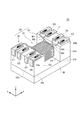
図1は、本発明の好ましい実施形態によるコイル部品10の外観構造を示す略斜視図である。
FIG. 1 is a schematic perspective view showing an external structure of a
本実施形態によるコイル部品10は表面実装型のパルストランスであり、図1に示すように、ドラム型コア20と、ドラム型コア20に接着された板状コア30と、ドラム型コア20の巻芯部21に巻回されたワイヤW1〜W4とを備えている。但し、本発明によるコイル部品がパルストランスに限定されるものではなく、バルントランスや昇圧トランスなどの他のトランス部品であっても構わないし、コモンモードチョークコイルなどのフィルタ部品であっても構わない。
The
ドラム型コア20及び板状コア30は、比較的透磁率の高い磁性材料、例えばNi−Zn系フェライトや、Mn−Zn系フェライトの焼結体によって構成されている。なお、Mn−Zn系フェライトなどの透磁率の高い磁性材料は、固有抵抗が低く導電性を有しているのが通常である。
The
ドラム型コア20は、y方向を軸方向とする棒状の巻芯部21と、巻芯部21のy方向における両端に設けられた第1及び第2の鍔部22,23とを備え、これらが一体化された構造を有している。鍔部22は、巻芯部21に接続される内側面22iと、内側面22iの反対側に位置する外側面22oと、巻芯部21の軸方向と平行な底面22bと、底面22bの反対側に位置する上面22tとを有する。同様に、鍔部23は、巻芯部21に接続される内側面23iと、内側面23iの反対側に位置する外側面23oと、巻芯部21の軸方向と平行な底面23bと、底面23bの反対側に位置する上面23tとを有する。内側面22i,23i及び外側面22o,23oはxz平面を構成し、底面22b,23b及び上面22t,23tはxy平面を構成する。
The
コイル部品10は、実使用時においてプリント基板上に表面実装される部品であり、鍔部22,23の底面22b,23bを基板に対向させた状態で実装される。鍔部22,23の上面22t,23tには、板状コア30が接着剤により固着されている。このような構造により、ドラム型コア20と板状コア30によって閉磁路が構成される。
The
図1に示すように、鍔部22の底面22b及び外側面22oには第1〜第4の端子電極E1〜E4がy方向にこの順に設けられ、鍔部23の底面23b及び外側面23oには第5〜第8の端子電極E5〜E8がy方向にこの順に設けられる。端子電極E1〜E8はいずれもL字型の端子金具からなり、接着剤を介して鍔部22又は23に接着されている。L字型の端子金具を用いることにより、ペースト状の金属を焼き付けることによって端子電極E1〜E8を形成する場合と比べて製造コストを低減することが可能となる。
As shown in FIG. 1, first to fourth terminal electrodes E1 to E4 are provided in this order in the y direction on the
巻芯部21には4本のワイヤW1〜W4が巻回されている。ワイヤW1〜W4の一端はそれぞれ端子電極E1〜E4の異なる一つに接続され、ワイヤW1〜W4の他端はそれぞれ端子電極E5〜E8の異なる一つに接続される。ワイヤW1〜W4の継線は、端子電極E1〜E8のうち底面22b,23bを覆う部分にて行われる。継線の方法については特に限定されないが、熱圧着又はレーザー接合により行うことができる。
Four wires W1 to W4 are wound around the
特に限定されるものではないが、ワイヤW1は端子電極E1及び端子電極E8に接続され、その巻回方向は例えば時計回りである。ワイヤW2は端子電極E2及び端子電極E7に接続され、その巻回方向は例えば反時計回りである。ワイヤW3は端子電極E3及び端子電極E6に接続され、その巻回方向は例えば時計回りである。ワイヤW4は端子電極E4及び端子電極E5に接続され、その巻回方向は例えば反時計回りである。 Although not particularly limited, the wire W1 is connected to the terminal electrode E1 and the terminal electrode E8, and the winding direction thereof is, for example, clockwise. The wire W2 is connected to the terminal electrode E2 and the terminal electrode E7, and the winding direction is, for example, counterclockwise. The wire W3 is connected to the terminal electrode E3 and the terminal electrode E6, and the winding direction thereof is, for example, clockwise. The wire W4 is connected to the terminal electrode E4 and the terminal electrode E5, and the winding direction is, for example, counterclockwise.
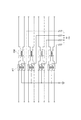
図2及び図3は、コイル部品10をy方向から見た側面図である。このうち、図2は鍔部22側から見た図であり、図3は鍔部23側から見た図である。
2 and 3 are side views of the
図2には、端子電極E1〜E4のレイアウトが詳細に示されている。具体的には、端子電極E1と端子電極E2とのx方向における距離をL1とし、端子電極E3と端子電極E4とのx方向における距離をL4とした場合、本実施形態によるコイル部品10は、
L1>L4
を満たしている。
FIG. 2 shows the layout of the terminal electrodes E1 to E4 in detail. Specifically, when the distance in the x direction between the terminal electrode E1 and the terminal electrode E2 is L1, and the distance in the x direction between the terminal electrode E3 and the terminal electrode E4 is L4, the
L1> L4
Meet.
また、巻芯部21の中心軸Aを通ってz方向に延在する仮想線C1を外側面22oに定義した場合、仮想線C1と端子電極E2のx方向における距離をL2とし、仮想線C1と端子電極E3のx方向における距離をL3とした場合、本実施形態によるコイル部品10は、
L2<L3
を満たしている。尚、
L1<L2+L3
である。
Further, when a virtual line C1 extending in the z direction through the central axis A of the
L2 <L3
Meet. still,
L1 <L2 + L3
It is.
さらに、外側面22oのx方向における右側端部と端子電極E1のx方向における距離をL5とし、外側面22oのx方向における左側端部と端子電極E4のx方向における距離をL6とした場合、本実施形態によるコイル部品10は、
L5>L6
を満たしている。
Further, when the distance in the x direction between the right end in the x direction of the outer surface 22o and the terminal electrode E1 is L5, and the distance in the x direction between the left end in the x direction of the outer surface 22o and the terminal electrode E4 is L6, The
L5> L6
Meet.
さらに、端子電極E1〜E4は、y方向から見て巻芯部21と重複しないよう、そのz方向における長さが短く設計されている。
Further, the terminal electrodes E1 to E4 are designed to have a short length in the z direction so as not to overlap with the
図3には、端子電極E5〜E8のレイアウトが詳細に示されている。具体的には、端子電極E5と端子電極E6とのx方向における距離をL1とし、端子電極E7と端子電極E8とのx方向における距離をL4とした場合、本実施形態によるコイル部品10は、
L1>L4
を満たしている。
FIG. 3 shows the layout of the terminal electrodes E5 to E8 in detail. Specifically, when the distance in the x direction between the terminal electrode E5 and the terminal electrode E6 is L1, and the distance in the x direction between the terminal electrode E7 and the terminal electrode E8 is L4, the
L1> L4
Meet.
また、巻芯部21の中心軸Aを通ってz方向に延在する仮想線C2を外側面23oに定義した場合、仮想線C2と端子電極E6のx方向における距離をL2とし、仮想線C2と端子電極E7のx方向における距離をL3とした場合、本実施形態によるコイル部品10は、
L2<L3
を満たしている。尚、
L1<L2+L3
である。
Further, when a virtual line C2 extending in the z direction through the central axis A of the
L2 <L3
Meet. still,
L1 <L2 + L3
It is.
さらに、外側面23oのx方向における右側端部と端子電極E5のx方向における距離をL5とし、外側面23oのx方向における左側端部と端子電極E8のx方向における距離をL6とした場合、本実施形態によるコイル部品10は、
L5>L6
を満たしている。
Furthermore, when the distance in the x direction between the right end in the x direction of the outer surface 23o and the terminal electrode E5 is L5, and the distance in the x direction between the left end in the x direction of the outer surface 23o and the terminal electrode E8 is L6, The
L5> L6
Meet.
さらに、端子電極E5〜E8は、y方向から見て巻芯部21と重複しないよう、そのz方向における長さが短く設計されている。
Further, the terminal electrodes E5 to E8 are designed to have a short length in the z direction so as not to overlap with the
本実施形態においては、端子電極E1〜E8がこのようなレイアウトを有していることから、例えば端子電極E1,E2をパルストランスの1次側入出力端子、端子電極E5,E6をパルストランスの2次側入出力端子、端子電極E7,E8をパルストランスの1次側センタータップ、端子電極E3,E4をパルストランスの2次側センタータップとして用いた場合に、1次側と2次側との間の絶縁耐圧を確保しつつ、渦電流によって生じる損失を低減することができる。1次側と2次側との間の絶縁耐圧を確保は、主に、距離L2+L3を距離L1や距離L2よりも拡大することによって実現される。 In the present embodiment, since the terminal electrodes E1 to E8 have such a layout, for example, the terminal electrodes E1 and E2 are the primary input / output terminals of the pulse transformer, and the terminal electrodes E5 and E6 are the pulse transformer. When the secondary input / output terminal, terminal electrodes E7 and E8 are used as the primary center tap of the pulse transformer, and terminal electrodes E3 and E4 are used as the secondary center tap of the pulse transformer, the primary side and the secondary side The loss caused by the eddy current can be reduced while ensuring the dielectric strength between the two. Ensuring the withstand voltage between the primary side and the secondary side is realized mainly by increasing the distance L2 + L3 over the distance L1 and the distance L2.
渦電流は、ワイヤW1〜W4に流れる電流よって生じた磁束が端子電極E1〜E8と錯交することにより生じる。しかしながら、本実施形態によるコイル部品10は、端子電極E1〜E8がy方向から見て巻芯部21と重複しないようレイアウトされていることから、渦電流の発生が抑制される。
The eddy current is generated when the magnetic flux generated by the current flowing through the wires W1 to W4 intersects with the terminal electrodes E1 to E8. However, since the
また、y方向から見て端子電極E1〜E8が巻芯部21と重複していない場合であっても、渦電流の発生をできる限り抑制するためには、y方向から見た端子電極E1〜E8の平面位置を巻芯部21の中心軸Aからできるだけ遠ざけることが好ましい。そのためには、例えば端子電極E1,E2を図2に示す右側にできるだけ寄せ、端子電極E3,E4を図2に示す左側にできるだけ寄せればよいが、端子電極E1,E2をパルストランスの1次側入出力端子として用いる場合、両者間の距離L1を近づけすぎると、一対の1次側入出力端子がショートするおそれが生じる。このため、端子電極E1と端子電極E2の距離L1については、ある程度の大きさを確保する必要がある。
Further, even when the terminal electrodes E1 to E8 are not overlapped with the winding
これに対し、端子電極E3,E4については、パルストランスの2次側センタータップとして用いる場合、両者には同電位が与えられる。したがって、端子電極E3と端子電極E4の距離L4については、距離L1よりも狭くすることが可能である(L1>L4)。これにより、端子電極E2に比べてより端子電極E3をより外側にオフセットして配置することができる(L3>L2)。このため、端子電極E3,E4と巻芯部21の中心軸Aとの距離が遠くなることから、端子電極E3,E4にて発生する渦電流を低減することが可能となる。
On the other hand, when the terminal electrodes E3 and E4 are used as secondary center taps of the pulse transformer, the same potential is applied to both. Therefore, the distance L4 between the terminal electrode E3 and the terminal electrode E4 can be made smaller than the distance L1 (L1> L4). As a result, the terminal electrode E3 can be arranged to be offset more outward than the terminal electrode E2 (L3> L2). For this reason, since the distance between the terminal electrodes E3 and E4 and the central axis A of the
しかも、端子電極E3,E4をパルストランスの2次側センタータップとして用いる場合、両者は同電位となることから、そのレイアウトは端子電極E1,E2よりも設計自由度が高い。この点を利用し、本実施形態においては、端子電極E4をより端部に寄せて配置しており(L5>L6)、これにより、端子電極E3,E4にて発生する渦電流をよりいっそう低減することが可能となる。 In addition, when the terminal electrodes E3 and E4 are used as the secondary center tap of the pulse transformer, since both have the same potential, the layout has a higher degree of design freedom than the terminal electrodes E1 and E2. Utilizing this point, in the present embodiment, the terminal electrode E4 is disposed closer to the end (L5> L6), and thereby, eddy currents generated at the terminal electrodes E3 and E4 are further reduced. It becomes possible to do.
端子電極E5〜E8についても同様であり、端子電極E7を端子電極E6に比べてより外側にオフセットして配置していることから、端子電極E7,E8にて発生する渦電流を低減することが可能となる。また、端子電極E8をより端部に寄せて配置することにより、端子電極E7,E8にて発生する渦電流をよりいっそう低減することが可能となる。 The same applies to the terminal electrodes E5 to E8, and since the terminal electrode E7 is arranged offset to the outside as compared with the terminal electrode E6, the eddy current generated in the terminal electrodes E7 and E8 can be reduced. It becomes possible. Further, by arranging the terminal electrode E8 closer to the end, it is possible to further reduce eddy currents generated in the terminal electrodes E7 and E8.
以上が本実施形態によるコイル部品10の構造である。
The above is the structure of the
図4は、コイル部品10が実装される基板上の導体パターンを示す平面図である。
FIG. 4 is a plan view showing a conductor pattern on a substrate on which the
図4に示す例では、基板40に2つの実装領域41,42が割り当てられており、これら実装領域41,42にそれぞれコイル部品10が実装される。実装領域41,42は、基板40上における高密度実装を実現すべく、互いにx方向に近接してレイアウトされている。具体的には、実装領域41と実装領域42のx方向における間隔はL0である。間隔L0の最小値は、求められる信頼性、仕様、実装精度などによって制限される。
In the example shown in FIG. 4, two mounting
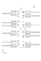
このようなレイアウトが必要な例としては、本実施形態によるコイル部品10がパルストランスである場合、図5に示すLANコネクタ回路(100Base)や、図6に示すLANコネクタ回路(1000Base)が挙げられる。これらのLANコネクタ回路は、図5及び図6に示すように、複数のパルストランスPTが用いられることから、高密度実装すると図4に示すように実装領域41,42が近接することがある。
Examples where such a layout is required include the LAN connector circuit (100Base) shown in FIG. 5 and the LAN connector circuit (1000Base) shown in FIG. 6 when the
実装領域41,42には、ハンダによって端子電極E1〜E8に接続されるランドパターンP1〜P6が設けられている。具体的には、ランドパターンP1,P2,P4,P5はそれぞれ端子電極E1,E2,E5,E6に接続され、ランドパターンP3は端子電極E3,E4に共通に接続され、ランドパターンP6は端子電極E7,E8に共通に接続される。これにより、端子電極E1,E2をパルストランスの1次側入出力端子、端子電極E5,E6をパルストランスの2次側入出力端子、端子電極E7,E8をパルストランスの1次側センタータップ、端子電極E3,E4をパルストランスの2次側センタータップとして用いることができる。
The mounting
図4に示すように、ランドパターンP3,P6は、他のランドパターンP1,P2,P4,P5よりもx方向における幅が拡大されている。これは、1つのランドパターン(例えばP3)に2つの端子電極(例えばE3,E4)を接続するためである。但し、ランドパターンP3,P6のx方向における幅としては、対応する2つの端子電極の全てを覆う幅とする必要はなく、図4に示すように、対応する2つの端子電極のそれぞれ一部を覆う幅とすれば足りる。これによれば、実装領域41,42間の距離L0が狭く、且つ、端子電極E4,E8と実装領域41,42のエッジとの距離L6が狭い場合であっても、実装領域41に設けられたランドパターンP1と実装領域42に設けられたランドパターンP3とのx方向における距離や、実装領域41に設けられたランドパターンP6と実装領域42に設けられたランドパターンP4とのx方向における距離を確保することができる。
As shown in FIG. 4, the land patterns P3 and P6 have a larger width in the x direction than the other land patterns P1, P2, P4 and P5. This is because two terminal electrodes (for example, E3 and E4) are connected to one land pattern (for example, P3). However, the width in the x direction of the land patterns P3 and P6 does not have to be a width that covers all of the corresponding two terminal electrodes. As shown in FIG. It is enough if it is the width to cover. According to this, even when the distance L0 between the mounting
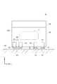
図7は、基板40に実装されたコイル部品10の側面図である。
FIG. 7 is a side view of the
図7に示す例では、端子電極E1とランドパターンP1がハンダ51によって接続され、端子電極E2とランドパターンP2がハンダ52によって接続され、端子電極E3,E4とランドパターンP3がハンダ53によって接続されている。このうち、ランドパターンP1,P2は、それぞれ対応する端子電極E1,E2よりもx方向におけるサイズが大きい。一方、ランドパターンP3については、端子電極E3と端子電極E4との間を覆うように配置されている。そして、これらランドパターンP1〜P3にそれぞれ供給されたハンダ51〜53は、鍔部22の外側面22oにおいてz方向に延在する端子電極E1〜E4の表面に覆ってフィレットを形成することから、基板40に対するコイル部品10の接続強度が強くなり、回路基板の信頼性を高めることが可能となる。
In the example shown in FIG. 7, the terminal electrode E1 and the land pattern P1 are connected by the
また、ハンダ53のフィレットは、端子電極E3と端子電極E4を直接接続するブリッジを形成する。このようなブリッジは、端子電極E3と端子電極E4の距離L4が狭い場合、容易に形成される。これにより、端子電極E3,E4は、ランドパターンP3を介して短絡されるだけでなく、ハンダ53のブリッジを介して短絡されることから、より確実な短絡が実現される。
The fillet of the
以上、本発明の好ましい実施形態について説明したが、本発明は、上記の実施形態に限定されることなく、本発明の主旨を逸脱しない範囲で種々の変更が可能であり、それらも本発明の範囲内に包含されるものであることはいうまでもない。 The preferred embodiments of the present invention have been described above, but the present invention is not limited to the above-described embodiments, and various modifications can be made without departing from the spirit of the present invention. Needless to say, it is included in the range.
例えば、上記実施形態によるコイル部品10は、端子電極E1〜E8としてL字型の端子金具を用いているが、L字型の端子金具を用いる代わりに、鍔部22,23にペースト状の金属を焼き付けることによって端子電極E1〜E8を形成しても構わない。
For example, the
また、上記実施形態によるコイル部品10は板状コア30を備えているが、本発明によるコイル部品がこれを備えることは必須でない。板状コア30を備える場合であっても、その位置については上記実施形態のように鍔部22,23の上面22t,23tであることは必須でなく、鍔部22と鍔部23を繋ぐように鍔部22,23のyz側面に設けても構わないし、鍔部22,23の上面22t,23tとyz側面の両方に設けても構わない。両方に設ける場合、鍔部22,23の上面22t,23tを覆う部分とyz側面を覆う部分が一体化した、断面がL字型の板状コアを用いても構わない。
Moreover, although the
さらに、端子電極E1〜E8がL字型であることも必須ではない。例えば、端子電極E1〜E4については鍔部22の上面22tをさらに覆い、端子電極E5〜E8については鍔部23の上面23tをさらに覆うような、コの字型であっても構わない。
Furthermore, it is not essential that the terminal electrodes E1 to E8 are L-shaped. For example, the terminal electrodes E1 to E4 may be U-shaped so as to further cover the
10 コイル部品
20 ドラム型コア
21 巻芯部
22,23 鍔部
22b,23b 底面
22i,23i 内側面
22o,23o 外側面
22t,23t 上面
30 板状コア
40 基板
41,42 実装領域
51〜53 ハンダ
A 中心軸
C1,C2 仮想線
E1〜E8 端子電極
P1〜P6 ランドパターン
PT パルストランス
W1〜W4 ワイヤ
DESCRIPTION OF
Claims (8)
前記第1の鍔部に形成され、前記第1の方向と直交する第2の方向にこの順に配列された第1乃至第4の端子電極と、
前記第2の鍔部に形成され、前記第2の方向にこの順に配列された第5乃至第8の端子電極と、
前記巻芯部に巻回され、一端がそれぞれ前記第1乃至第4の端子電極の異なる一つに接続され、他端がそれぞれ前記第5乃至第8の端子電極の異なる一つに接続された第1乃至第4のワイヤと、を備え、
前記第1の鍔部は、前記巻芯部に接続された第1の内側面と、前記第1の内側面とは反対側に位置する第1の外側面とを有し、
前記第2の鍔部は、前記巻芯部に接続された第2の内側面と、前記第2の内側面とは反対側に位置する第2の外側面とを有し、
前記第1乃至第4の端子電極は、少なくとも前記第1の外側面に形成され、
前記第5乃至第8の端子電極は、少なくとも前記第2の外側面に形成され、
前記第1の端子電極と前記第2の端子電極の前記第2の方向における距離は、前記第3の端子電極と前記第4の端子電極の前記第2の方向における距離よりも広く、
前記第5の端子電極と前記第6の端子電極の前記第2の方向における距離は、前記第7の端子電極と前記第8の端子電極の前記第2の方向における距離よりも広く、
前記第1及び第2の方向と直交する第3の方向に延在し、且つ、前記第2の方向における位置が前記巻芯部の中心軸と一致した第1の仮想線を前記第1の外側面に定義した場合、前記第1の仮想線と前記第3の端子電極の前記第2の方向における距離は、前記第1の仮想線と前記第2の端子電極の前記第2の方向における距離よりも広く、
前記第3の方向に延在し、且つ、前記第2の方向における位置が前記巻芯部の中心軸と一致した第2の仮想線を前記第2の外側面に定義した場合、前記第2の仮想線と前記第7の端子電極の前記第2の方向における距離は、前記第2の仮想線と前記第6の端子電極の前記第2の方向における距離よりも広いことを特徴とするコイル部品。 A winding core portion having the first direction as an axial direction, a first flange portion provided at one end of the winding core portion in the first direction, and the other end of the winding core portion in the first direction. A drum-type core including a second collar portion provided on
First to fourth terminal electrodes formed in the first flange and arranged in this order in a second direction orthogonal to the first direction;
Fifth to eighth terminal electrodes formed in the second flange and arranged in this order in the second direction;
Wound around the core, one end connected to a different one of the first to fourth terminal electrodes, and the other end connected to a different one of the fifth to eighth terminal electrodes, respectively. First to fourth wires,
The first flange portion has a first inner surface connected to the core portion, and a first outer surface located on the opposite side of the first inner surface,
The second flange portion has a second inner surface connected to the core portion, and a second outer surface located on the opposite side to the second inner surface,
The first to fourth terminal electrodes are formed on at least the first outer surface,
The fifth to eighth terminal electrodes are formed on at least the second outer surface,
The distance between the first terminal electrode and the second terminal electrode in the second direction is wider than the distance between the third terminal electrode and the fourth terminal electrode in the second direction,
The distance between the fifth terminal electrode and the sixth terminal electrode in the second direction is wider than the distance between the seventh terminal electrode and the eighth terminal electrode in the second direction,
A first imaginary line extending in a third direction orthogonal to the first and second directions and having a position in the second direction coinciding with the central axis of the core portion is defined as the first imaginary line. When defined on the outer surface, the distance between the first imaginary line and the third terminal electrode in the second direction is the distance between the first imaginary line and the second terminal electrode in the second direction. Wider than the distance,
When the second imaginary line extending in the third direction and whose position in the second direction coincides with the central axis of the core portion is defined on the second outer surface, the second The distance between the imaginary line and the seventh terminal electrode in the second direction is wider than the distance between the second imaginary line and the sixth terminal electrode in the second direction. parts.
前記第8の端子電極と前記第2の外側面の前記第2の方向における一方の端部との距離は、前記第5の端子電極と前記第2の外側面の前記第2の方向における他方の端部との距離よりも狭いことを特徴とする請求項1又は2に記載のコイル部品。 The distance between the fourth terminal electrode and one end of the first outer surface in the second direction is the other of the first terminal electrode and the first outer surface in the second direction. Narrower than the distance to the end of
The distance between the eighth terminal electrode and one end of the second outer surface in the second direction is the other of the fifth terminal electrode and the second outer surface in the second direction. The coil component according to claim 1, wherein the coil component is narrower than a distance from an end of the coil component.
前記第2の鍔部は、前記第1及び第2の方向と平行な第2の底面をさらに有し、
前記第1乃至第4の端子電極は、前記第1の底面にさらに形成され、
前記第5乃至第8の端子電極は、前記第2の底面にさらに形成され、
前記第1乃至第4のワイヤの前記一端は、前記第1の底面に形成された前記第1乃至第4の端子電極にそれぞれ継線され、
前記第1乃至第4のワイヤの前記他端は、前記第2の底面に形成された前記第5乃至第8の端子電極にそれぞれ継線されていることを特徴とする請求項1乃至3のいずれか一項に記載のコイル部品。 The first flange further has a first bottom surface parallel to the first and second directions,
The second flange further has a second bottom surface parallel to the first and second directions,
The first to fourth terminal electrodes are further formed on the first bottom surface,
The fifth to eighth terminal electrodes are further formed on the second bottom surface,
The one ends of the first to fourth wires are respectively connected to the first to fourth terminal electrodes formed on the first bottom surface;
4. The other ends of the first to fourth wires are respectively connected to the fifth to eighth terminal electrodes formed on the second bottom surface. The coil component according to any one of the above.
前記第5乃至第8の端子電極は、前記第2の外側面及び前記第2の底面を覆うL字型の端子金具からなることを特徴とする請求項4に記載のコイル部品。 The first to fourth terminal electrodes are L-shaped terminal fittings that cover the first outer surface and the first bottom surface,
5. The coil component according to claim 4, wherein the fifth to eighth terminal electrodes are L-shaped terminal fittings that cover the second outer side surface and the second bottom surface. 6.
前記第1の鍔部は、前記第1の底面とは反対側に位置する第1の上面をさらに有し、
前記第2の鍔部は、前記第2の底面とは反対側に位置する第2の上面をさらに有し、
前記板状コアは、前記第1及び第2の上面に接着されていることを特徴とする請求項4又は5に記載のコイル部品。 It further comprises a plate core,
The first flange further has a first upper surface located on the opposite side of the first bottom surface,
The second flange further has a second upper surface located on the opposite side of the second bottom surface,
6. The coil component according to claim 4, wherein the plate-like core is bonded to the first and second upper surfaces.
前記基板に実装された請求項1乃至6のいずれか一項に記載のコイル部品と、
前記複数のランドパターンと前記第1乃至第8の端子電極とをそれぞれ接続するハンダと、を備え、
前記複数のランドパターンは、前記第1、第2、第5及び第6の端子電極にそれぞれ接続される第1、第2、第3及び第4のランドパターンと、前記第3及び第4の端子電極に共通に接続される第5のランドパターンと、前記第7及び第8の端子電極に共通に接続される第6のランドパターンとを含むことを特徴とする回路基板。 A substrate having a plurality of land patterns;
The coil component according to any one of claims 1 to 6 mounted on the substrate;
Solder for connecting the plurality of land patterns and the first to eighth terminal electrodes, respectively.
The plurality of land patterns include first, second, third, and fourth land patterns connected to the first, second, fifth, and sixth terminal electrodes, respectively, and the third and fourth land patterns. A circuit board comprising: a fifth land pattern commonly connected to a terminal electrode; and a sixth land pattern commonly connected to the seventh and eighth terminal electrodes.
Priority Applications (4)
| Application Number | Priority Date | Filing Date | Title |
|---|---|---|---|
| JP2016000324A JP6733179B2 (en) | 2016-01-05 | 2016-01-05 | Coil component and circuit board including the same |
| US15/395,045 US9839129B2 (en) | 2016-01-05 | 2016-12-30 | Coil component and circuit board having the same |
| CN201710004196.5A CN107039153B (en) | 2016-01-05 | 2017-01-04 | Coil component and the circuit board for having the coil component |
| US15/803,818 US10123422B2 (en) | 2016-01-05 | 2017-11-05 | Coil component and circuit board having the same |
Applications Claiming Priority (1)
| Application Number | Priority Date | Filing Date | Title |
|---|---|---|---|
| JP2016000324A JP6733179B2 (en) | 2016-01-05 | 2016-01-05 | Coil component and circuit board including the same |
Publications (2)
| Publication Number | Publication Date |
|---|---|
| JP2017123365A true JP2017123365A (en) | 2017-07-13 |
| JP6733179B2 JP6733179B2 (en) | 2020-07-29 |
Family
ID=59236008
Family Applications (1)
| Application Number | Title | Priority Date | Filing Date |
|---|---|---|---|
| JP2016000324A Active JP6733179B2 (en) | 2016-01-05 | 2016-01-05 | Coil component and circuit board including the same |
Country Status (3)
| Country | Link |
|---|---|
| US (2) | US9839129B2 (en) |
| JP (1) | JP6733179B2 (en) |
| CN (1) | CN107039153B (en) |
Cited By (3)
| Publication number | Priority date | Publication date | Assignee | Title |
|---|---|---|---|---|
| JP2020009903A (en) * | 2018-07-09 | 2020-01-16 | Tdk株式会社 | Pulse transformer and circuit module with the same |
| JP2021118255A (en) * | 2020-01-27 | 2021-08-10 | Tdk株式会社 | Coil component and circuit board including the same |
| JP7444012B2 (en) | 2020-09-30 | 2024-03-06 | 株式会社村田製作所 | coil parts |
Families Citing this family (5)
| Publication number | Priority date | Publication date | Assignee | Title |
|---|---|---|---|---|
| CN110416772A (en) * | 2018-04-29 | 2019-11-05 | 深南电路股份有限公司 | A kind of connector and electronic device |
| TWM575180U (en) * | 2018-11-19 | 2019-03-01 | 美磊科技股份有限公司 | Magnetic component |
| JP7363559B2 (en) * | 2020-02-18 | 2023-10-18 | Tdk株式会社 | Coil parts and circuit boards equipped with the same |
| JP7156327B2 (en) * | 2020-03-12 | 2022-10-19 | 株式会社村田製作所 | Winding cores and coil parts with electrodes |
| CN117174457A (en) * | 2022-05-25 | 2023-12-05 | 绵阳普思电子有限公司 | Patch type transformer |
Citations (9)
| Publication number | Priority date | Publication date | Assignee | Title |
|---|---|---|---|---|
| JPS6339937Y2 (en) * | 1982-01-20 | 1988-10-19 | ||
| JPH0187576U (en) * | 1987-12-02 | 1989-06-09 | ||
| JP2001044046A (en) * | 1999-07-29 | 2001-02-16 | Taiyo Yuden Co Ltd | Coil part and hybrid integrated circuit device mounting the same |
| JP2004363178A (en) * | 2003-06-02 | 2004-12-24 | Murata Mfg Co Ltd | Winding coil component |
| JP2010093216A (en) * | 2008-10-10 | 2010-04-22 | Tdk Corp | Coil component and method of manufacturing the same |
| JP2010109267A (en) * | 2008-10-31 | 2010-05-13 | Tdk Corp | Surface-mounted pulse transformer, and method and apparatus for manufacturing the same |
| US20130049914A1 (en) * | 2011-08-22 | 2013-02-28 | Hon Hai Precision Industry Co., Ltd. | Surface mounted pulse transformer |
| JP2014192324A (en) * | 2013-03-27 | 2014-10-06 | Tdk Corp | Pulse transformer |
| JP2014204124A (en) * | 2013-04-01 | 2014-10-27 | 台達電子工業股▲ふん▼有限公司Delta Electronics,Inc. | Transformer |
Family Cites Families (12)
| Publication number | Priority date | Publication date | Assignee | Title |
|---|---|---|---|---|
| EP1077455B1 (en) * | 1999-08-19 | 2007-10-17 | Murata Manufacturing Co., Ltd. | Coil component |
| US20080309445A1 (en) * | 2007-06-14 | 2008-12-18 | Tdk Corporation | Transformer |
| JP4708469B2 (en) * | 2008-02-29 | 2011-06-22 | Tdk株式会社 | Balun Trans |
| JP4888843B2 (en) * | 2009-08-24 | 2012-02-29 | Tdk株式会社 | Trance |
| CN202258716U (en) * | 2011-08-22 | 2012-05-30 | 富士康(昆山)电脑接插件有限公司 | Pulse transformer |
| CN203456223U (en) * | 2012-10-16 | 2014-02-26 | Tdk株式会社 | Pulse transformer |
| JP5771232B2 (en) * | 2013-03-29 | 2015-08-26 | Tdk株式会社 | Pulse transformer |
| TWI473127B (en) * | 2013-03-29 | 2015-02-11 | Delta Electronics Inc | Transformer device |
| JP6357950B2 (en) * | 2014-04-03 | 2018-07-18 | Tdk株式会社 | Coil parts |
| JP6435649B2 (en) * | 2014-06-05 | 2018-12-12 | Tdk株式会社 | Coil component and manufacturing method thereof |
| US10186376B2 (en) * | 2015-07-10 | 2019-01-22 | Tdk Corporation | Coil component comprising a plurality of coated conductive wires and manufacturing method thereof |
| JP6642006B2 (en) * | 2016-01-05 | 2020-02-05 | Tdk株式会社 | Coil component and circuit board having the same |
-
2016
- 2016-01-05 JP JP2016000324A patent/JP6733179B2/en active Active
- 2016-12-30 US US15/395,045 patent/US9839129B2/en active Active
-
2017
- 2017-01-04 CN CN201710004196.5A patent/CN107039153B/en active Active
- 2017-11-05 US US15/803,818 patent/US10123422B2/en active Active
Patent Citations (9)
| Publication number | Priority date | Publication date | Assignee | Title |
|---|---|---|---|---|
| JPS6339937Y2 (en) * | 1982-01-20 | 1988-10-19 | ||
| JPH0187576U (en) * | 1987-12-02 | 1989-06-09 | ||
| JP2001044046A (en) * | 1999-07-29 | 2001-02-16 | Taiyo Yuden Co Ltd | Coil part and hybrid integrated circuit device mounting the same |
| JP2004363178A (en) * | 2003-06-02 | 2004-12-24 | Murata Mfg Co Ltd | Winding coil component |
| JP2010093216A (en) * | 2008-10-10 | 2010-04-22 | Tdk Corp | Coil component and method of manufacturing the same |
| JP2010109267A (en) * | 2008-10-31 | 2010-05-13 | Tdk Corp | Surface-mounted pulse transformer, and method and apparatus for manufacturing the same |
| US20130049914A1 (en) * | 2011-08-22 | 2013-02-28 | Hon Hai Precision Industry Co., Ltd. | Surface mounted pulse transformer |
| JP2014192324A (en) * | 2013-03-27 | 2014-10-06 | Tdk Corp | Pulse transformer |
| JP2014204124A (en) * | 2013-04-01 | 2014-10-27 | 台達電子工業股▲ふん▼有限公司Delta Electronics,Inc. | Transformer |
Cited By (5)
| Publication number | Priority date | Publication date | Assignee | Title |
|---|---|---|---|---|
| JP2020009903A (en) * | 2018-07-09 | 2020-01-16 | Tdk株式会社 | Pulse transformer and circuit module with the same |
| JP7052607B2 (en) | 2018-07-09 | 2022-04-12 | Tdk株式会社 | Pulse transformer and circuit module equipped with it |
| JP2021118255A (en) * | 2020-01-27 | 2021-08-10 | Tdk株式会社 | Coil component and circuit board including the same |
| JP7409110B2 (en) | 2020-01-27 | 2024-01-09 | Tdk株式会社 | Coil parts and circuit boards equipped with the same |
| JP7444012B2 (en) | 2020-09-30 | 2024-03-06 | 株式会社村田製作所 | coil parts |
Also Published As
| Publication number | Publication date |
|---|---|
| JP6733179B2 (en) | 2020-07-29 |
| CN107039153A (en) | 2017-08-11 |
| US10123422B2 (en) | 2018-11-06 |
| CN107039153B (en) | 2018-10-02 |
| US20170196093A1 (en) | 2017-07-06 |
| US20180070451A1 (en) | 2018-03-08 |
| US9839129B2 (en) | 2017-12-05 |
Similar Documents
| Publication | Publication Date | Title |
|---|---|---|
| JP6733179B2 (en) | Coil component and circuit board including the same | |
| US9865386B2 (en) | Coil component and circuit board having the same | |
| US9196415B2 (en) | Coil component | |
| US9736942B2 (en) | Coil component, its manufacturing method, and circuit substrate provided with the coil component | |
| JP6551142B2 (en) | Coil component and circuit board incorporating the same | |
| JP6554947B2 (en) | Coil component and manufacturing method thereof | |
| JP7139666B2 (en) | coil parts | |
| US20190089320A1 (en) | Common mode filter | |
| US10453600B2 (en) | Differential mode filter | |
| US10366823B2 (en) | Coil component | |
| US10389328B2 (en) | Differential mode filter | |
| US9812244B2 (en) | Multilayer inductor device | |
| JP6919194B2 (en) | Coil parts and circuit boards equipped with them | |
| JP2017147321A (en) | Coil component, circuit board incorporating coil component, and power supply circuit including coil component | |
| JP2019220665A (en) | Coil component | |
| US11521787B2 (en) | Coil component | |
| US20220301766A1 (en) | Coil component | |
| JP2019213186A (en) | Electronic component and electronic control unit | |
| JP4021746B2 (en) | Circuit board mounting structure for power supply coil components | |
| JP6669312B2 (en) | Module parts and power supply circuit | |
| JP6211238B1 (en) | choke coil | |
| JP2022034595A (en) | Coil component | |
| WO2018047372A1 (en) | Choke coil | |
| JP2019220664A (en) | Coil component |
Legal Events
| Date | Code | Title | Description |
|---|---|---|---|
| A621 | Written request for application examination |
Free format text: JAPANESE INTERMEDIATE CODE: A621 Effective date: 20181005 |
|
| A977 | Report on retrieval |
Free format text: JAPANESE INTERMEDIATE CODE: A971007 Effective date: 20190425 |
|
| A131 | Notification of reasons for refusal |
Free format text: JAPANESE INTERMEDIATE CODE: A131 Effective date: 20190528 |
|
| A521 | Request for written amendment filed |
Free format text: JAPANESE INTERMEDIATE CODE: A523 Effective date: 20190722 |
|
| A02 | Decision of refusal |
Free format text: JAPANESE INTERMEDIATE CODE: A02 Effective date: 20200107 |
|
| A521 | Request for written amendment filed |
Free format text: JAPANESE INTERMEDIATE CODE: A523 Effective date: 20200318 |
|
| A911 | Transfer to examiner for re-examination before appeal (zenchi) |
Free format text: JAPANESE INTERMEDIATE CODE: A911 Effective date: 20200325 |
|
| TRDD | Decision of grant or rejection written | ||
| A01 | Written decision to grant a patent or to grant a registration (utility model) |
Free format text: JAPANESE INTERMEDIATE CODE: A01 Effective date: 20200609 |
|
| A61 | First payment of annual fees (during grant procedure) |
Free format text: JAPANESE INTERMEDIATE CODE: A61 Effective date: 20200622 |
|
| R150 | Certificate of patent or registration of utility model |
Ref document number: 6733179 Country of ref document: JP Free format text: JAPANESE INTERMEDIATE CODE: R150 |