JP2017118348A - Antenna device - Google Patents
Antenna device Download PDFInfo
- Publication number
- JP2017118348A JP2017118348A JP2015252339A JP2015252339A JP2017118348A JP 2017118348 A JP2017118348 A JP 2017118348A JP 2015252339 A JP2015252339 A JP 2015252339A JP 2015252339 A JP2015252339 A JP 2015252339A JP 2017118348 A JP2017118348 A JP 2017118348A
- Authority
- JP
- Japan
- Prior art keywords
- antenna
- power
- signal
- transmission
- transmitter
- Prior art date
- Legal status (The legal status is an assumption and is not a legal conclusion. Google has not performed a legal analysis and makes no representation as to the accuracy of the status listed.)
- Granted
Links
Images


Landscapes
- Variable-Direction Aerials And Aerial Arrays (AREA)
Abstract
Description
本発明は、アクティブフェーズドアレーアンテナ(APAA:Active Phased Array Antenna)を含むアンテナ装置に関する。 The present invention relates to an antenna apparatus including an active phased array antenna (APAA).
従来のAPPA装置では、アンテナ開口面に実装されている複数の送受信モジュールの各々を制御し、使用する送受信モジュール数を周波数によって可変にすることで開口面を制限して低消費電力化を図ることが検討されている。 In a conventional APPA device, each of a plurality of transmission / reception modules mounted on an antenna aperture surface is controlled, and the number of transmission / reception modules to be used is made variable according to the frequency, thereby limiting the aperture surface and reducing power consumption. Is being considered.
特許文献1には、「周波数が高くなるとアンテナ開口面積を小さくしてビーム幅を所定の大きさ以下にしないようにすることで、高い周波数においても送信ビームを対象目標に当てることを容易にした広帯域アクティブフェーズドアレーアンテナ装置を提供する」ことを課題とし、「APAAでの送受信の周波数が所定値未満の場合は全てのアンテナ素子を動作させる全開口とし、所定値以上の場合は動作させるアンテナ素子を制限して部分開口としてAPAAのビーム幅を規定値以下にしないよう制御するビーム制御器4を備えた」広帯域APAA装置が開示されている。
しかしながら、上記従来の技術によれば、低消費電力化は可能であるものの、周波数に応じてアンテナの開口面積が変化する。そのため、周波数の変化に応じて開口面積が変化し、ビーム幅が変化してしまう、という問題があった。 However, according to the above conventional technique, although the power consumption can be reduced, the aperture area of the antenna changes according to the frequency. Therefore, there is a problem that the aperture area changes according to the change in frequency, and the beam width changes.
本発明は、上記に鑑みてなされたものであって、ビーム幅を一定としてレーダ性能を維持しつつ低消費電力化を実現したアンテナ装置を得ることを目的とする。 The present invention has been made in view of the above, and an object of the present invention is to obtain an antenna device that realizes low power consumption while maintaining radar performance with a constant beam width.
上述した課題を解決し、目的を達成するために、本発明は、RF(Radio Frequency)信号を送信する送信器と、前記送信器に接続されて電磁波を送受信する空中線と、前記空中線に電力を供給する電源器と、前記空中線を制御する信号処理器とを備え、前記空中線は、前記送信器から送信された前記RF信号を分配する給電回路と、電源制御分配回路と、前記RF信号の位相及び振幅を制御する複数個の送受信モジュールと、送信時には制御された前記RF信号を空中に放射して受信時には電磁波を受信する複数個の素子アンテナとを備え、余剰の出力電力が存在する周波数帯域においては、前記空中線に必要とされる電力及び前記複数個の送受信モジュールの出力電力から前記信号処理器が補正値を求め、この補正値による補正後のパルスドRF信号で動作することを特徴とする。 In order to solve the above-described problems and achieve the object, the present invention provides a transmitter for transmitting an RF (Radio Frequency) signal, an antenna connected to the transmitter for transmitting and receiving electromagnetic waves, and power to the antenna. A power supply unit that supplies the signal, and a signal processor that controls the antenna. The antenna includes a power feeding circuit that distributes the RF signal transmitted from the transmitter, a power control distribution circuit, and a phase of the RF signal. And a plurality of transmission / reception modules for controlling amplitude, and a plurality of element antennas for radiating the controlled RF signal in the air at the time of transmission and receiving electromagnetic waves at the time of reception, and a frequency band in which surplus output power exists , The signal processor obtains a correction value from the power required for the antenna and the output power of the plurality of transmission / reception modules. Characterized in that it operates in pulsed RF signal after correction.
本発明によれば、ビーム幅を一定としてレーダ性能を維持しつつ低消費電力化を実現したアンテナ装置を得ることができるという効果を奏する。 According to the present invention, it is possible to obtain an antenna device that realizes low power consumption while maintaining radar performance with a constant beam width.
以下に、本発明の実施の形態にかかるアンテナ装置を図面に基づいて詳細に説明する。なお、この実施の形態によりこの発明が限定されるものではない。 Hereinafter, an antenna device according to an embodiment of the present invention will be described in detail with reference to the drawings. Note that the present invention is not limited to the embodiments.
実施の形態1.
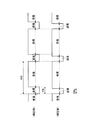
図1は、本発明の実施の形態1に係るアンテナ装置の構成の一例を示す図である。図1に示すアンテナ装置は、RF信号を送信する送信器1と、送信器1からのRF信号が入力されて電磁波を送受信する空中線2と、空中線2に電力を供給する電源器3と、制御信号を送受信して空中線2を制御する信号処理器4とを備える。空中線2は、送信器1から入力されたRF信号を分配する給電回路5と、電源器3から入力される電力及び信号処理器4から入力される制御信号を分配する電源制御分配回路6と、RF信号の位相及び振幅を制御するN個の送受信モジュール7−1から7−Nと、送信時には位相及び振幅が制御されたRF信号を電磁波として空中に放射して受信時には空中から電磁波を受信する素子アンテナ8−1から8−Nとを備える。なお、振幅の制御は、振幅の増幅を含む。
FIG. 1 is a diagram illustrating an example of a configuration of an antenna device according to
送信器1は給電回路5に接続され、電源器3及び信号処理器4は電源制御分配回路6に接続されている。給電回路5の分配端の各々は、N個の送受信モジュール7−1から7−Nの各々と接続され、送受信モジュール7−1から7−Nの各々は、素子アンテナ8−1から8−Nに接続されている。電源制御分配回路6の分配端の各々は、送受信モジュール7−1から7−Nに接続されている。
The
次に、図1に示すアンテナ装置の動作の一例について説明する。送信器1からは、送信と受信との繰り返し周期期間に占める送信期間の割合を示すデューティDで生成されたパルスドRF信号が出力される。このパルスドRF信号は空中線2の給電回路5に入力されてN分配され、N分配された制御信号は送受信モジュール7−1から7−Nの各々に入力される。送受信モジュール7−1から7−Nに入力されたパルスドRF信号は、モジュール出力電力PMDL(i)に増幅されて素子アンテナ8−1から8−Nに入力され、素子アンテナ8−1から8−Nを用いて空中に放射される。ここで、iは1≦i≦Nの自然数であり、以下の説明においても同様である。
Next, an example of the operation of the antenna device illustrated in FIG. 1 will be described. The
次に、送信器1から出力されるパルスドRF信号について説明する。図2は、実施の形態1におけるパルスドRF信号のデューティを説明する図である。図2に示すように、デューティDは、補正前においては送信期間のパルス幅PW及び送信と受信とのパルス繰り返し周期期間PRIを用いて下記の式(1)で表される。
Next, the pulsed RF signal output from the
![]()
![]()
本実施の形態1においては、送信器1は、補正値kによってパルスドRF信号を補正して出力する。送信器1は、図2に示す補正後のパルス幅PWaのように送信期間を変化させたパルスドRF信号を空中線2に出力する。補正後のデューティDaは、補正前のデューティD及び補正値kを用いて下記の式(2)で表される。
In the first embodiment, the
![]()
![]()
ここで、補正値kについて説明する。レーダ探知距離及びレーダ反射断面積(RCS:Radar Cross−Section)といったレーダ性能要求によって、システム設計上最低限必要となる空中線送信電力Ptは、下記の式(3)に示すように、各モジュール出力電力の最小値Pmin(i)の総和で表される。 Here, the correction value k will be described. Antenna transmission power Pt, which is the minimum required for system design, due to radar performance requirements such as radar detection distance and radar reflection cross-section (RCS), is shown in the following equation (3). It is represented by the sum of the minimum power value P min (i).

このとき、実効放射電力EIRPminは、下記の式(4)に示すように、素子アンテナ利得Geと、空中線送信電力Ptと、効率ηと、損失Lとの積で表される。 At this time, the effective radiated power EIRP min is represented by the product of the element antenna gain Ge, the antenna transmission power Pt, the efficiency η, and the loss L as shown in the following formula (4).
![]()
![]()
そして、レーダ性能から最低限必要となる平均出力電力Paveは、下記の式(5)に示すように、実効放射電力EIRPminとデューティDとの積で表される。 The average output power P ave that is minimum required from the radar performance is expressed by the product of the effective radiated power EIRP min and the duty D as shown in the following equation (5).
![]()
![]()
一方で、上記の式(3)に示す空中線送信電力Ptは、各送受信モジュールのモジュール出力電力PMDL(i)に応じて変化する。図3は、本実施の形態1における送受信モジュールの周波数に対する出力電力の特性の一例を示す図である。図3に示すように、規定の出力電力に対して余剰の出力電力が存在する周波数帯域においては、デューティD及び出力電力PMDL(i)は変更可能であるため、システム設計上最低限必要となる空中線送信電力Ptを維持することが可能である。 On the other hand, the antenna transmission power Pt shown in the above equation (3) changes according to the module output power P MDL (i) of each transmission / reception module. FIG. 3 is a diagram illustrating an example of output power characteristics with respect to the frequency of the transmission / reception module according to the first embodiment. As shown in FIG. 3, the duty D and the output power PMDL (i) can be changed in a frequency band where surplus output power exists with respect to the specified output power. It is possible to maintain the antenna transmission power Pt.
ここで、空中線2の各送受信モジュールのモジュール出力電力PMDL(i)を測定し、空中線送信電力Ptを用いて、信号処理器4が下記の式(6)により補正値kを算出する。
Here, the module output power P MDL (i) of each transmission / reception module of the
補正値k<1であるため、図2の補正後のデューティDaのパルス幅PWaは短くなり、電源器3から空中線2に供給される平均の消費電力を小さくすることが可能となる。
Since the correction value k <1, the pulse width PWa of the corrected duty Da in FIG. 2 is shortened, and the average power consumption supplied from the
したがって、送信モジュール7−1から7−Nが規定の出力電力に対して余剰の出力電力がある周波数帯域では補正値kを算出し、補正前のデューティDから補正後のデューティDaに変更することによりレーダ性能を維持しつつ低消費電力化が可能である。 Therefore, the transmission module 7-1 to 7-N calculates the correction value k in the frequency band where there is surplus output power relative to the specified output power, and changes the duty D before correction to the duty Da after correction. As a result, low power consumption can be achieved while maintaining radar performance.
なお、補正値kは、空中線2の空中線有効放射電力を実測し、この空中線有効放射電力実測値PANT、空中線送信電力Pt及び空中線利得GANTを用いて、下記の式(7)により算出することも可能である。
The correction value k is calculated by the following equation (7) by actually measuring the antenna effective radiation power of the
以上説明した本実施の形態1のアンテナ装置は、RF信号を送信する送信器1と、送信器1に接続されて電磁波を送受信する空中線2と、空中線2に電力を供給する電源器3と、空中線2に制御信号を送受信する信号処理器4とを備える。空中線2は、送信器1から送信されたRF信号を分配する給電回路5と、電源器3から入力される電力及び信号処理器4から入力される制御信号を分配する電源制御分配回路6と、RF信号の位相及び振幅を制御する複数個の送受信モジュール7−1から7−Nと、送信時には制御されたRF信号を空中に放射して受信時には空中から電磁波を受信する素子アンテナ8−1から8−Nとを備え、余剰の出力電力が存在する周波数帯域においては、空中線2に必要とされる電力及び複数個の送受信モジュール7−1から7−Nの出力電力から信号処理器4が補正値kを求め、この補正値kによる補正後のパルスドRF信号で動作する。このように動作することで、ビーム幅を一定としてレーダ性能を維持しつつ低消費電力化を実現することができる。
The antenna device according to the first embodiment described above includes a
実施の形態2.
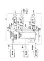
図4は、本発明の実施の形態2に係るアンテナ装置の構成の一例を示す図である。図4に示すアンテナ装置は、図1に示すアンテナ装置の空中線2に代えて空中線2aを備え、空中線2aは、電源制御分配回路6に代えて電源制御分配回路6aを備える。電源制御分配回路6aは、電圧可変回路9及びメモリ10を備える。電圧可変回路9は電源器3に接続され、電圧可変回路9の各々は送受信モジュール7−1から7−Nの各々に接続されている。また、メモリ10は、電圧可変回路9に接続されている。
FIG. 4 is a diagram showing an example of the configuration of the antenna device according to
次に、図4に示すアンテナ装置の動作の一例について説明する。送受信モジュール7−1から7−Nの各々の出力特性は、図3に示すように周波数特性を有する。図3に示すように、送受信モジュール7−1から7−Nの各々の出力特性は、一般に送受信モジュール7−1から7−Nに電源器3から供給される送信用電力の電圧の影響を受ける。そのため、周波数毎に各送受信モジュール7−1から7−Nの出力電力が規定値以上且つ必要最低限の一定の出力電力になるように送信用電力の電圧を調整して設定電圧値を生成する。そして、各周波数の出力電力に対する設定電圧値のデータをメモリ10に全て保存し、そのデータを電圧可変回路9にロードする。次に、電圧可変回路9にて各周波数帯域における、送受信モジュール7−1から7−Nの各々の電圧を制御し、出力電力を一定にする。なお、電圧の制御は、送受信モジュール7−1から7−Nの各々にレギュレータを設けて、このレギュレータの調整抵抗の各々を調整することによって行ってもよいし、分圧抵抗の接続を直接にスイッチ制御してもよい。このようにして、空中線2の送信電力を適切な一定値に保つことが可能であり、余剰の消費電力を削減することができる。
Next, an example of the operation of the antenna device illustrated in FIG. 4 will be described. Each output characteristic of the transmission / reception modules 7-1 to 7-N has a frequency characteristic as shown in FIG. As shown in FIG. 3, the output characteristics of each of the transmission / reception modules 7-1 to 7-N are generally affected by the voltage of the transmission power supplied from the
以上説明した本実施の形態2のアンテナ装置の電源制御分配回路6aは、電源器3からの電力が供給される電圧可変回路9と、送信用電源電圧と出力特性との関係が記録されたメモリ10とを備え、電圧可変回路9により空中線2の送信電力が一定値となるように制御することで、余剰の消費電力を削減し、ビーム幅を一定としてレーダ性能を維持しつつ低消費電力化を実現することができる。
The power control distribution circuit 6a of the antenna device according to the second embodiment described above includes the voltage variable circuit 9 to which the power from the
以上実施の形態1,2によれば、ビーム幅を一定としてレーダ性能を維持しつつ、各周波数帯域における余剰の出力電力分からパルスドRF信号のデューティの補正値を算出し、補正を行ったデューティで送信を行うことで、低消費電力化を実現することができる。また、低消費電力化を行うことで、冷却系及び電源系の必要性能を低く抑えることができ、性能上の過剰な設計を行うことなく適切な設計が可能となる。そのため、冷却系及び電源系の装置の小型化及び低コスト化が可能となり、レーダシステムの小型化及び低コスト化が可能となる。 According to the first and second embodiments, the correction value of the duty of the pulsed RF signal is calculated from the excess output power in each frequency band while maintaining the radar performance with a constant beam width, and the corrected duty is used. By performing transmission, low power consumption can be realized. Further, by reducing the power consumption, the required performance of the cooling system and the power supply system can be kept low, and an appropriate design can be performed without performing an excessive design in performance. Therefore, it is possible to reduce the size and cost of the cooling system and the power supply system, and it is possible to reduce the size and cost of the radar system.
以上の実施の形態に示した構成は、本発明の内容の一例を示すものであり、別の公知の技術と組み合わせることも可能であるし、本発明の要旨を逸脱しない範囲で、構成の一部を省略、変更することも可能である。 The configuration described in the above embodiment shows an example of the contents of the present invention, and can be combined with another known technique, and can be combined with other configurations without departing from the gist of the present invention. It is also possible to omit or change the part.
1 送信器、2,2a 空中線、3 電源器、4 信号処理器、5 給電回路、6,6a 電源制御分配回路、7−1,7−2,7−N 送受信モジュール、8−1,8−2,8−N 素子アンテナ、9 電圧可変回路、10 メモリ。
DESCRIPTION OF
Claims (4)
前記送信器に接続されて電磁波を送受信する空中線と、
前記空中線に電力を供給する電源器と、
前記空中線に制御信号を送受信する信号処理器とを備え、
前記空中線は、
前記送信器から送信された前記RF信号を分配する給電回路と、
前記電源器から入力される電力及び前記信号処理器から入力される前記制御信号を分配する電源制御分配回路と、
前記RF信号の位相及び振幅を制御する複数個の送受信モジュールと、
送信時には制御された前記RF信号を空中に放射して受信時には空中から電磁波を受信する複数個の素子アンテナとを備え、
余剰の出力電力が存在する周波数帯域においては、前記空中線に必要とされる電力及び前記複数個の送受信モジュールの出力電力から前記信号処理器が補正値を求め、この補正値による補正後のパルスドRF信号で動作することを特徴とするアンテナ装置。 A transmitter for transmitting an RF signal;
An antenna connected to the transmitter for transmitting and receiving electromagnetic waves;
A power supply for supplying power to the antenna;
A signal processor for transmitting and receiving control signals to the antenna,
The antenna is
A power feeding circuit for distributing the RF signal transmitted from the transmitter;
A power control distribution circuit for distributing the power input from the power supply and the control signal input from the signal processor;
A plurality of transceiver modules for controlling the phase and amplitude of the RF signal;
A plurality of element antennas that radiate the controlled RF signal into the air during transmission and receive electromagnetic waves from the air during reception;
In a frequency band where surplus output power exists, the signal processor obtains a correction value from the power required for the antenna and the output power of the plurality of transmission / reception modules, and the pulsed RF corrected by the correction value is obtained. An antenna device characterized by operating with a signal.
前記電源器からの電力が供給される電圧可変回路と、
送信用電源電圧と出力特性との関係が記録されたメモリとを備え、
前記電圧可変回路により前記空中線の送信電力が一定となるように制御することを特徴とする請求項1に記載のアンテナ装置。 The power control distribution circuit includes:
A voltage variable circuit to which power from the power supply is supplied;
A memory in which the relationship between the power supply voltage for transmission and the output characteristics is recorded;
The antenna device according to claim 1, wherein the voltage variable circuit controls the antenna so that transmission power of the antenna becomes constant.
Priority Applications (1)
| Application Number | Priority Date | Filing Date | Title |
|---|---|---|---|
| JP2015252339A JP6559059B2 (en) | 2015-12-24 | 2015-12-24 | Antenna device |
Applications Claiming Priority (1)
| Application Number | Priority Date | Filing Date | Title |
|---|---|---|---|
| JP2015252339A JP6559059B2 (en) | 2015-12-24 | 2015-12-24 | Antenna device |
Publications (2)
| Publication Number | Publication Date |
|---|---|
| JP2017118348A true JP2017118348A (en) | 2017-06-29 |
| JP6559059B2 JP6559059B2 (en) | 2019-08-14 |
Family
ID=59234664
Family Applications (1)
| Application Number | Title | Priority Date | Filing Date |
|---|---|---|---|
| JP2015252339A Active JP6559059B2 (en) | 2015-12-24 | 2015-12-24 | Antenna device |
Country Status (1)
| Country | Link |
|---|---|
| JP (1) | JP6559059B2 (en) |
Citations (2)
| Publication number | Priority date | Publication date | Assignee | Title |
|---|---|---|---|---|
| JP2005227232A (en) * | 2004-02-16 | 2005-08-25 | Mitsubishi Electric Corp | Radar equipment |
| JP2015195464A (en) * | 2014-03-31 | 2015-11-05 | 三菱電機株式会社 | antenna device |
-
2015
- 2015-12-24 JP JP2015252339A patent/JP6559059B2/en active Active
Patent Citations (2)
| Publication number | Priority date | Publication date | Assignee | Title |
|---|---|---|---|---|
| JP2005227232A (en) * | 2004-02-16 | 2005-08-25 | Mitsubishi Electric Corp | Radar equipment |
| JP2015195464A (en) * | 2014-03-31 | 2015-11-05 | 三菱電機株式会社 | antenna device |
Also Published As
| Publication number | Publication date |
|---|---|
| JP6559059B2 (en) | 2019-08-14 |
Similar Documents
| Publication | Publication Date | Title |
|---|---|---|
| US12140692B2 (en) | Antenna device and radar apparatus | |
| US7456787B2 (en) | Beam-forming antenna with amplitude-controlled antenna elements | |
| US9997843B2 (en) | Band-selective aperture shading for sidelobe reduction in TX/RX phased array satellite communications transceivers | |
| JP6456579B1 (en) | Phased array antenna | |
| CN103618559B (en) | A kind of radio frequency front-end device based on directional antenna and communication control method thereof | |
| US10469183B1 (en) | Antenna device and method for calibrating antenna device | |
| US10673139B2 (en) | Phased array system and beam scanning method | |
| KR20170003837A (en) | Transmission array system for beamforming and method for controlling output power | |
| JP5796759B2 (en) | Active phased array antenna device | |
| KR20160086557A (en) | Apparatus for adjusting radiation pattern of a radar antenna and a radar apparatus for a vehicle | |
| CN106463826B (en) | Antenna device with adjustable radiation characteristics and method for operating the antenna device | |
| US10658763B2 (en) | Per-element power control for array based communications | |
| JP6465819B2 (en) | ANTENNA DEVICE AND POWER CONTROL METHOD | |
| JP6559059B2 (en) | Antenna device | |
| JP3514973B2 (en) | Active array antenna device | |
| JP2013005059A (en) | Radio communication device, transmission method and program | |
| KR101007213B1 (en) | Antenna combiner for multiple radiation patterns in radar systems | |
| JP2014137336A (en) | Tactical air navigation ground device, and waveform control system for tactical air navigation transmission output signal | |
| JP7259275B2 (en) | Phased array antenna device, power transmission system, beam pattern forming method, and power transmission method | |
| US11955999B2 (en) | Device for controlling a scanning active antenna | |
| JP2664570B2 (en) | Antenna device | |
| CN114069234A (en) | An L-band Power-Weighted Low Sidelobe Antenna Array | |
| JP3634047B2 (en) | Grating lobe cancel antenna for mobile SNG | |
| JP2001124845A (en) | Radar device | |
| JP2015197404A (en) | Antenna device |
Legal Events
| Date | Code | Title | Description |
|---|---|---|---|
| A621 | Written request for application examination |
Free format text: JAPANESE INTERMEDIATE CODE: A621 Effective date: 20171228 |
|
| A977 | Report on retrieval |
Free format text: JAPANESE INTERMEDIATE CODE: A971007 Effective date: 20181108 |
|
| A131 | Notification of reasons for refusal |
Free format text: JAPANESE INTERMEDIATE CODE: A131 Effective date: 20181120 |
|
| A521 | Request for written amendment filed |
Free format text: JAPANESE INTERMEDIATE CODE: A523 Effective date: 20190118 |
|
| TRDD | Decision of grant or rejection written | ||
| A01 | Written decision to grant a patent or to grant a registration (utility model) |
Free format text: JAPANESE INTERMEDIATE CODE: A01 Effective date: 20190618 |
|
| A61 | First payment of annual fees (during grant procedure) |
Free format text: JAPANESE INTERMEDIATE CODE: A61 Effective date: 20190716 |
|
| R150 | Certificate of patent or registration of utility model |
Ref document number: 6559059 Country of ref document: JP Free format text: JAPANESE INTERMEDIATE CODE: R150 |
|
| R250 | Receipt of annual fees |
Free format text: JAPANESE INTERMEDIATE CODE: R250 |
|
| R250 | Receipt of annual fees |
Free format text: JAPANESE INTERMEDIATE CODE: R250 |
|
| R250 | Receipt of annual fees |
Free format text: JAPANESE INTERMEDIATE CODE: R250 |
|
| R250 | Receipt of annual fees |
Free format text: JAPANESE INTERMEDIATE CODE: R250 |