JP2017116751A - Interference type optical circuit and control method thereof - Google Patents
Interference type optical circuit and control method thereof Download PDFInfo
- Publication number
- JP2017116751A JP2017116751A JP2015252568A JP2015252568A JP2017116751A JP 2017116751 A JP2017116751 A JP 2017116751A JP 2015252568 A JP2015252568 A JP 2015252568A JP 2015252568 A JP2015252568 A JP 2015252568A JP 2017116751 A JP2017116751 A JP 2017116751A
- Authority
- JP
- Japan
- Prior art keywords
- output
- waveguide
- light
- duplexer
- photodetector
- Prior art date
- Legal status (The legal status is an assumption and is not a legal conclusion. Google has not performed a legal analysis and makes no representation as to the accuracy of the status listed.)
- Granted
Links
Images


Abstract
Description
本発明は、干渉型光回路およびその制御方法に関し、より詳細には、マッハツェンダ干渉計光導波路など光の干渉効果を利用する干渉型光回路およびその制御方法に関する。 The present invention relates to an interferometric optical circuit and a control method thereof, and more particularly to an interferometric optical circuit using a light interference effect such as a Mach-Zehnder interferometer optical waveguide and a control method thereof.
マッハツェンダ干渉計光導波路に代表される、光の干渉効果を利用する干渉型光回路は、光デバイスの重要な構成要素である。例えば、マッハツェンダ干渉計は、適当な分波回路によって、入力された光を2分岐させ、アーム導波路と呼ばれる2本の光導波路を、別々に導波させる。2本のアーム導波路からの光を合波器で再び合波させるが、合波される2つの光波の位相差によって、合波器から出力される光の強度、位相が変化する。また、合波器が複数の出力導波路を有している場合には、合波器から出力される光の出力導波路が変化する。 An interferometric optical circuit that utilizes the interference effect of light, represented by a Mach-Zehnder interferometer optical waveguide, is an important component of an optical device. For example, a Mach-Zehnder interferometer splits input light into two by an appropriate branching circuit, and separately guides two optical waveguides called arm waveguides. The light from the two arm waveguides is recombined by the multiplexer, but the intensity and phase of the light output from the multiplexer are changed by the phase difference between the two light waves to be combined. Further, when the multiplexer has a plurality of output waveguides, the output waveguide of the light output from the multiplexer changes.
マッハツェンダ干渉計を用いて、2つの光波の位相を外部信号によって変化させて、外部信号によって出力光の状態を制御したり、アーム導波路の位相特性に強い波長依存性を持たせて波長制御素子としたり、偏光依存性を持たせて偏光制御素子とすることができる。ただし、アーム導波路の位相特性を設計通りに作製することは、作製揺らぎの観点から困難であり、実際はアーム導波路に外部信号を加えることにより、その屈折率を変化させて、アーム導波路の位相誤差を補償する方法が採られている。 Using a Mach-Zehnder interferometer, the phase of two light waves is changed by an external signal, the state of the output light is controlled by the external signal, or the phase characteristic of the arm waveguide is made to have a strong wavelength dependence, thereby controlling the wavelength. Or a polarization control element having polarization dependency. However, it is difficult to produce the phase characteristics of the arm waveguide as designed from the viewpoint of fluctuation of production, and in fact, by adding an external signal to the arm waveguide, its refractive index is changed, and the arm waveguide A method for compensating for the phase error is employed.
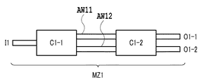
図1に、従来のマッハツェンダ干渉計を示す。マッハツェンダ干渉計MZ1は、1つの入力ポートI1を有する分波器C1−1と、2つの出力ポートO1−1およびO1−2を有する合波器C1−2と、分波器C1−1と合波器C1−2との間を接続する2本のアーム導波路AW11およびAW12とを備えている(例えば、非特許文献1参照)。MZ1に入力された光は、所定の割合で出力ポートO1−1とO1−2とから出力されるが、一般的には、アーム導波路AW11およびAW12の作製揺らぎにより、出力ポートO1−1とO1−2から出力される光の割合は、作製した素子毎にランダムな誤差を有する。 FIG. 1 shows a conventional Mach-Zehnder interferometer. The Mach-Zehnder interferometer MZ1 includes a duplexer C1-1 having one input port I1, a duplexer C1-2 having two output ports O1-1 and O1-2, and a duplexer C1-1. Two arm waveguides AW11 and AW12 that connect the waver C1-2 are provided (for example, see Non-Patent Document 1). The light input to the MZ1 is output from the output ports O1-1 and O1-2 at a predetermined ratio. Generally, however, the output ports O1-1 and OW12 are connected to the output ports O1-1 and AW12 by fluctuations in the fabrication of the arm waveguides AW11 and AW12. The ratio of the light output from O1-2 has a random error for each manufactured device.
例えば、出力ポートO1−1からの光出力を最大化したい場合には、アーム導波路AW11,AW12に適当な制御信号を印加することにより、マッハツェンダ干渉計MZ1における光の干渉状態を変化させて、アーム導波路AW11,AW12を伝搬する光の位相を制御する。原理的には、出力ポートO1−1からの光出力を最大化すると、出力ポートO1−2からの光出力が最小化される。このことから、出力ポートO1−2からの光出力の強度をモニタリングし、これを最小化するようにアーム導波路AW11,AW12に加える信号を調整して、出力ポートO1−1からの光出力を最大化することができる。具体的には、出力ポートO1−2に光を吸収して電流に変換するモニタ用フォトディテクタを配置する。フォトディテクタからの光電流が最小値になるように、アーム導波路AW11,AW12への信号を制御する。 For example, when it is desired to maximize the optical output from the output port O1-1, by applying an appropriate control signal to the arm waveguides AW11 and AW12, the light interference state in the Mach-Zehnder interferometer MZ1 is changed. The phase of light propagating through the arm waveguides AW11 and AW12 is controlled. In principle, when the optical output from the output port O1-1 is maximized, the optical output from the output port O1-2 is minimized. From this, the intensity of the optical output from the output port O1-2 is monitored, the signal applied to the arm waveguides AW11 and AW12 is adjusted so as to minimize this, and the optical output from the output port O1-1 is adjusted. Can be maximized. Specifically, a monitor photodetector that absorbs light and converts it into current is arranged at the output port O1-2. Signals to the arm waveguides AW11 and AW12 are controlled so that the photocurrent from the photodetector becomes a minimum value.
しかしながら、実際には、出力ポートO1−2からの光出力が最小値を取る場合でも、出力ポートO1−1からの光出力が最大にならない場合がある。その原因の1つが光デバイスの偏光依存性である。一般に光デバイスは、偏光依存性、すなわち伝搬する光電界の振動方向によって特性が異なるという特性を有している。図1のマッハツェンダ干渉計MZ1の場合を例にとると、入力される光の偏光状態の違いによって、アーム導波路AW11,AW12に同一の信号を加えたとしても、出力ポートO1−1,O1−2への光の出力の割合が異なる現象が起こり得る。 However, actually, even when the optical output from the output port O1-2 takes the minimum value, the optical output from the output port O1-1 may not become maximum. One of the causes is the polarization dependence of the optical device. In general, an optical device has a characteristic that it depends on polarization, that is, the characteristic varies depending on the vibration direction of a propagating optical electric field. Taking the case of the Mach-Zehnder interferometer MZ1 in FIG. 1 as an example, even if the same signal is applied to the arm waveguides AW11 and AW12 depending on the polarization state of the input light, the output ports O1-1 and O1- A phenomenon may occur in which the ratio of the light output to 2 is different.
図2に、従来のマッハツェンダ干渉計の透過特性を示す。図2(a)は、マッハツェンダ干渉計MZ1のTEモード(光電界が導波路の水平方向に平行)に対する透過特性を示し、図2(b)は、TMモード(光電界が導波路の水平方向に垂直)に対する透過特性を示している。図2の横軸は、制御信号強度であり、入力ポートI1にTEモードの光を入力しておき、透過特性の繰り返し周期を一周期分変化させるために必要な、アーム導波路AW11,AW12へ加える信号強度を100%としている。実際には、アーム導波路AW11,AW12へ加える電圧、電流の値に換算される。 FIG. 2 shows the transmission characteristics of a conventional Mach-Zehnder interferometer. 2A shows the transmission characteristics of the Mach-Zehnder interferometer MZ1 for the TE mode (the optical electric field is parallel to the horizontal direction of the waveguide), and FIG. 2B is the TM mode (the optical electric field is the horizontal direction of the waveguide). The transmission characteristics for (vertical) are shown. The horizontal axis in FIG. 2 is the control signal intensity. To the arm waveguides AW11 and AW12, which is necessary to input TE mode light to the input port I1 and change the repetition period of the transmission characteristics by one period. The applied signal strength is 100%. Actually, the values are converted into values of voltage and current applied to the arm waveguides AW11 and AW12.
図2(a),(b)を比較すると、アーム導波路AW11,AW12に信号を加えていない場合(制御信号強度0%)、出力ポートO1−1,O1−2への光出力の割合が、入力光のTEモードとTMモードという偏波によって異なる。また、アーム導波路AW11,AW12に同じ強度の制御信号を加えた場合、TMモードの方がアーム導波路間の光の位相差が大きく、透過率の変化が大きいことがわかる。 2A and 2B, when no signal is applied to the arm waveguides AW11 and AW12 (control signal intensity 0%), the ratio of the optical output to the output ports O1-1 and O1-2 is as follows. The input light differs depending on the polarization of TE mode and TM mode. In addition, when control signals having the same intensity are applied to the arm waveguides AW11 and AW12, it can be seen that the TM mode has a larger light phase difference between the arm waveguides and a greater change in transmittance.
図3に、従来のマッハツェンダ干渉計において偏波クロストークがある場合の透過特性を示す。図2に示した透過特性を有するマッハツェンダ干渉計MZ1に、TEモードの光とTMモードの光を10:1の割合で入力した際の透過率を示している。マッハツェンダ干渉計MZ1へ入力される光の偏波クロストークは10dBである。入力光に意図とは異なる偏波成分が含まれている状態、すなわち偏波クロストークを有していると、図3に示したように、偏光依存性のために、透過率の外部信号強度に対する曲線が歪んでいることが分かる。 FIG. 3 shows transmission characteristics when there is polarization crosstalk in the conventional Mach-Zehnder interferometer. The transmittance when TE mode light and TM mode light are input at a ratio of 10: 1 to the Mach-Zehnder interferometer MZ1 having the transmission characteristics shown in FIG. The polarization crosstalk of the light input to the Mach-Zehnder interferometer MZ1 is 10 dB. When the input light includes a polarization component different from the intended one, that is, when it has polarization crosstalk, as shown in FIG. It can be seen that the curve for is distorted.
図3において、偏波クロストークがある場合の出力ポートO1−2からの光出力は、制御信号強度が40%程度で最小値を取っている。一方、図2(a)のTEモードの光のみの透過率は、制御信号強度が50%で最小値を取っている。マッハツェンダ干渉計MZ1にTEモードの光を入力し、上述したように、出力ポートO1−2をモニタリングして出力ポートO1−1の光出力を制御する場合、入力光にTMモードが混ざっていると、出力ポートO1−2のモニタリングだけでは、出力ポートO1−1の光出力を正確に制御できないことがわかる。 In FIG. 3, the optical output from the output port O1-2 when there is polarization crosstalk takes the minimum value when the control signal intensity is about 40%. On the other hand, the transmittance of only the TE mode light in FIG. 2A takes the minimum value when the control signal intensity is 50%. When the TE mode light is input to the Mach-Zehnder interferometer MZ1 and the output port O1-2 is monitored to control the optical output of the output port O1-1 as described above, the TM mode is mixed with the input light. It can be seen that the optical output of the output port O1-1 cannot be accurately controlled only by monitoring the output port O1-2.
本発明の目的は、光導波路へ加えるべき制御信号の強さを、入力光の偏波クロストークの影響を取り除いて決定することができる干渉型光回路およびその制御方法を提供することにある。 An object of the present invention is to provide an interference type optical circuit that can determine the intensity of a control signal to be applied to an optical waveguide by removing the influence of polarization crosstalk of input light, and a control method therefor.
本発明は、このような目的を達成するために、一実施態様は、少なくとも1つの入力ポートを有する分波器と、少なくとも2つの出力ポートを有する合波器と、前記分波器と前記合波器との間を接続する複数のアーム導波路とを含む干渉型光回路であって、前記2つの出力ポートのうち第1の出力ポートに接続され、特定の偏光状態の光のみを吸収する偏光フィルタ導波路と、前記偏光フィルタ導波路の出力に接続されたフォトディテクタを備え、前記フォトディテクタからの光電流に応じて前記アーム導波路に制御信号を印加することにより、前記2つの出力ポートのうち第2の出力ポートの光出力を制御することを特徴とする。 According to the present invention, in order to achieve such an object, an embodiment includes a duplexer having at least one input port, a duplexer having at least two output ports, the duplexer, and the duplexer. An interferometric optical circuit including a plurality of arm waveguides connected to a waver, and is connected to a first output port of the two output ports and absorbs only light in a specific polarization state A polarization filter waveguide and a photodetector connected to the output of the polarization filter waveguide, and applying a control signal to the arm waveguide according to a photocurrent from the photodetector, The optical output of the second output port is controlled.
本発明によれば、特定の偏光状態の光のみを吸収する偏光フィルタ導波路とフォトディテクタとにより検出された光電流に応じて、アーム導波路に制御信号を印加するので、光導波路へ加えるべき制御信号の強さを、入力光の偏波クロストークの影響を取り除いて決定することができる。 According to the present invention, the control signal is applied to the arm waveguide according to the photocurrent detected by the polarization filter waveguide and the photodetector that absorbs only light of a specific polarization state, so that the control to be applied to the optical waveguide The signal strength can be determined by removing the influence of the polarization crosstalk of the input light.
以下、図面を参照しながら本発明の実施形態について詳細に説明する。 Hereinafter, embodiments of the present invention will be described in detail with reference to the drawings.
(第1の実施形態)
図4に、本発明の第1の実施形態にかかる干渉型光回路を示す。1x2ポート構成のマッハツェンダ干渉計MZは、1つの入力ポートIを有する分波器C1と、2つの出力ポートO1およびO2を有する合波器C2と、分波器C1と合波器C2との間を接続する2本のアーム導波路AW1およびAW2とを備えている。出力ポートO1には、偏光フィルタ導波路PFWを介して、モニタ用フォトディテクタMPDがモノリシック集積されている。分波器C1は、1x2のY分岐回路、2x2の光カプラを用いることができる。合波器C2は、2x2の光カプラを用いることができる。
(First embodiment)
FIG. 4 shows an interference optical circuit according to the first embodiment of the present invention. The Mach-Zehnder interferometer MZ having a 1 × 2 port configuration includes a duplexer C1 having one input port I, a duplexer C2 having two output ports O1 and O2, and a duplexer C1 and a duplexer C2. Are provided with two arm waveguides AW1 and AW2. A monitor photo detector MPD is monolithically integrated in the output port O1 via the polarization filter waveguide PFW. The duplexer C1 can use a 1 × 2 Y branch circuit and a 2 × 2 optical coupler. The multiplexer C2 can use a 2 × 2 optical coupler.
入力ポートIから入力された光は、マッハツェンダ干渉計MZに入力されて、分波器C1から所定の割合で、アーム導波路AW1およびAW2に出力される。入力光の波長は1.55μmであり、マッハツェンダ干渉計MZは図2に示した透過特性を有しているとする。出力ポートO2が干渉型光回路のメイン出力であり、アーム導波路AW1,AW2に適当な制御信号を印加することにより、マッハツェンダ干渉計MZにおける光の干渉状態を変化させて、アーム導波路AW1,AW2を伝搬する光の位相を制御する。出力ポートO1に接続されたモニタ用フォトディテクタMPDからの光電流量に応じて制御信号を印加し、出力ポートO2からの光出力を制御する。 The light input from the input port I is input to the Mach-Zehnder interferometer MZ, and is output from the duplexer C1 to the arm waveguides AW1 and AW2 at a predetermined ratio. The wavelength of the input light is 1.55 μm, and the Mach-Zehnder interferometer MZ has the transmission characteristics shown in FIG. The output port O2 is the main output of the interference optical circuit, and by applying an appropriate control signal to the arm waveguides AW1 and AW2, the interference state of the light in the Mach-Zehnder interferometer MZ is changed, and the arm waveguides AW1 and AW1 are changed. Controls the phase of light propagating through AW2. A control signal is applied in accordance with the photoelectric flow rate from the monitor photodetector MPD connected to the output port O1, and the light output from the output port O2 is controlled.
アーム導波路AW1,AW2における光の位相制御は、例えば、熱光学効果を利用する。アーム導波路AW1,AW2に沿ってヒータを配置し、ヒータへの電流を制御して、導波路内の屈折率を変化させ、導波路を伝播する光の位相を制御する。 The phase control of light in the arm waveguides AW1 and AW2 uses, for example, a thermo-optic effect. A heater is disposed along the arm waveguides AW1 and AW2, and the current to the heater is controlled to change the refractive index in the waveguide, thereby controlling the phase of light propagating through the waveguide.
図5は、第1の実施形態の干渉型光回路の光導波路を示す断面図である。基板S上にコア層COが形成され、さらにコア層CO上にクラッド層CLが形成されている。基板Sとしては、InPを選択する。基板Sの材料としては、シリコン、ガラスなどの他の材料でも構わない。コア層COは、0.5μm厚のInGaAsPであり、クラッド層CLは、2.0μm厚のInPである。ここで、光を閉じ込めるコア層COのInGaAsPは、フォトルミネッセント評価において1.3μmをピーク波長(バンドギャップ波長1.3μm)として発光する半導体組成を用いている。ドライエッチング工程などにより、図5の破線の形状に加工することにより、リッジ型の光導波路を形成する。このような構成の光導波路を用いて、分波器、合波器、アーム導波路、入出力ポートに接続される入出力導波路が形成されている。 FIG. 5 is a cross-sectional view showing the optical waveguide of the interference optical circuit of the first embodiment. A core layer CO is formed on the substrate S, and a cladding layer CL is formed on the core layer CO. InP is selected as the substrate S. As the material of the substrate S, other materials such as silicon and glass may be used. The core layer CO is InGaAsP having a thickness of 0.5 μm, and the cladding layer CL is InP having a thickness of 2.0 μm. Here, InGaAsP of the core layer CO that confines light uses a semiconductor composition that emits light with a peak wavelength of 1.3 μm (band gap wavelength of 1.3 μm) in the photoluminescence evaluation. A ridge type optical waveguide is formed by processing into the shape of the broken line in FIG. 5 by a dry etching process or the like. Using the optical waveguide having such a configuration, a duplexer, a multiplexer, an arm waveguide, and an input / output waveguide connected to the input / output port are formed.
偏光フィルタ導波路PFWの出力に接続されたモニタ用フォトディテクタMPDは、出力ポートO1に接続された出力導波路に形成されている。InP基板S上に干渉型光回路を形成しているので、InGaAsPコア層COの一部を、光導波路のバンドギャップ波長とは異なる1.55μmに近いバンドギャップ波長を有するInGaAsPに置き換えることにより、モニタ用フォトディテクタMPDをモノリシック集積している。基板Sがシリコンの場合は、コア層COとしてSiG層を堆積させることにより、フォトディテクタが得られる。基板Sがガラスの場合は、既存のベアチップ型のフォトディテクタを貼り付けることにより、フォトディテクタを集積することができる。このようにして、同一の基板S上に、分波器、合波器、アーム導波路等ともに、フォトディテクタをモノリシック集積することができる。 The monitor photodetector MPD connected to the output of the polarization filter waveguide PFW is formed in the output waveguide connected to the output port O1. Since the interference type optical circuit is formed on the InP substrate S, by replacing a part of the InGaAsP core layer CO with InGaAsP having a band gap wavelength close to 1.55 μm different from the band gap wavelength of the optical waveguide, The monitor photodetector MPD is monolithically integrated. When the substrate S is silicon, a photodetector is obtained by depositing a SiG layer as the core layer CO. When the substrate S is made of glass, the photodetector can be integrated by attaching an existing bare chip type photodetector. In this manner, the photodetector can be monolithically integrated on the same substrate S together with the duplexer, the multiplexer, the arm waveguide, and the like.
図6は、第1の実施形態の干渉型光回路の偏光フィルタ導波路を示す断面図である。偏光フィルタ導波路PFWは、出力ポートO1に接続された出力導波路において、図5に示したリッジ型の光導波路のクラッド層CLを1.5μm取り除き、その上から金を蒸着して金属クラッドMCLを形成してある。このようにして、同一の基板S上に、分波器、合波器、アーム導波路等ともに、偏光フィルタ導波路をモノリシック集積することができる。偏光フィルタは、特定の偏光の光を強く吸収するように設計されている。金属クラッドを有する導波路は、その損失に強い偏光依存性を有することが知られており、InP系導波路においては、TEモードとTMモードの間で吸収係数の差が2桁程度異なることが知られている(例えば、非特許文献2参照)。 FIG. 6 is a cross-sectional view showing a polarization filter waveguide of the interference optical circuit according to the first embodiment. The polarizing filter waveguide PFW is a metal clad MCL formed by removing 1.5 μm of the cladding layer CL of the ridge-type optical waveguide shown in FIG. 5 from the output waveguide connected to the output port O1, and depositing gold on it. Is formed. In this way, the polarization filter waveguide can be monolithically integrated on the same substrate S together with the duplexer, multiplexer, arm waveguide, and the like. A polarizing filter is designed to strongly absorb light of a specific polarization. A waveguide having a metal cladding is known to have a strong polarization dependence on its loss. In an InP-based waveguide, the difference in absorption coefficient between the TE mode and the TM mode may differ by about two orders of magnitude. It is known (see, for example, Non-Patent Document 2).
金属を光導波路のコア層の直上に付けることにより、TMモードに対する吸収係数がTEモードに対する吸収係数に対して大きくなる。図6に示したリッジ型の光導波路の固有モードを計算すると、TEモードの光パワーの減衰係数が2.5cm-1であるのに対して、TMモードの減衰量は80cm-1と計算される。従って、偏光フィルタ導波路PFWに沿って、光を300μm程度伝搬させれば、TMモードの光をTEモードと比較して10dB減衰させることができる。 By attaching metal directly on the core layer of the optical waveguide, the absorption coefficient for the TM mode becomes larger than the absorption coefficient for the TE mode. When the eigenmode of the ridge type optical waveguide shown in FIG. 6 is calculated, the attenuation coefficient of the optical power of the TE mode is 2.5 cm −1 , whereas the attenuation amount of the TM mode is calculated as 80 cm −1. The Therefore, if light is propagated along the polarization filter waveguide PFW by about 300 μm, TM mode light can be attenuated by 10 dB compared to the TE mode.
図7に、第1の実施形態の干渉型光回路において偏波クロストークがある場合の透過特性を示す。マッハツェンダ干渉計MZにおける偏波クロストークは10dBであり、偏光フィルタ導波路PFWからの出力の光透過特性である。図3に示した透過特性と比較すると、偏光フィルタ導波路PFWによってTMモード成分が除去され、透過特性の曲線の歪が解消されているのが分かる。TEモードの透過率が最小になる制御信号強度が50%となっており、図2(a)に示した透過特性と等しいことが分かる。 FIG. 7 shows the transmission characteristics when there is polarization crosstalk in the interference optical circuit of the first embodiment. The polarization crosstalk in the Mach-Zehnder interferometer MZ is 10 dB, which is the light transmission characteristic of the output from the polarization filter waveguide PFW. Compared with the transmission characteristics shown in FIG. 3, it can be seen that the TM mode component is removed by the polarization filter waveguide PFW and the distortion of the curve of the transmission characteristics is eliminated. It can be seen that the control signal intensity at which the TE mode transmittance is minimized is 50%, which is equal to the transmission characteristics shown in FIG.
従って、偏光フィルタ導波路PFWの出力に接続されたモニタ用フォトディテクタMPDからの光電流が最小となるように、アーム導波路AW1,AW2へ制御信号を印加すれば、出力導波路O2からのTEモードの成分が最大になり、マッハツェンダ干渉計MZを正確に制御することができる。 Accordingly, when a control signal is applied to the arm waveguides AW1 and AW2 so that the photocurrent from the monitor photodetector MPD connected to the output of the polarization filter waveguide PFW is minimized, the TE mode from the output waveguide O2 is applied. , And the Mach-Zehnder interferometer MZ can be accurately controlled.
マッハツェンダ干渉計MZにおける偏波クロストークが既知であれば、偏光フィルタ導波路PFWの導波路の長さを一意に決めることができる。また、偏波クロストークの値を正確に知ることができれば、アーム導波路AW1,AW2への制御信号を、偏波クロストークの値に応じて、調整することも考えられる。しかしながら、製造誤差、環境条件に依存する偏波クロストークの値を正確に知ることは難しい。 If the polarization crosstalk in the Mach-Zehnder interferometer MZ is known, the length of the polarization filter waveguide PFW can be uniquely determined. Further, if the value of the polarization crosstalk can be accurately known, the control signal to the arm waveguides AW1 and AW2 may be adjusted according to the value of the polarization crosstalk. However, it is difficult to accurately know the value of polarization crosstalk that depends on manufacturing errors and environmental conditions.
一方、偏波クロストークの値を正確に知ることができない場合でも、TMモードの光をある程度(例えば、10dB)減衰させることができる偏光フィルタ導波路を設置しておけば、偏波クロストークを減少させることができるので、出力導波路O2に対する制御の精度を向上させることができる。従って、本実施形態によれば、より簡便な方法により、偏波クロストークの影響を取り除くことができる。 On the other hand, if a polarization filter waveguide capable of attenuating TM mode light to some extent (for example, 10 dB) is installed even if the value of polarization crosstalk cannot be accurately known, polarization crosstalk can be reduced. Since it can reduce, the precision of control with respect to the output waveguide O2 can be improved. Therefore, according to this embodiment, the influence of polarization crosstalk can be removed by a simpler method.
図8に、偏光フィルタ導波路の別の実施例を示す。第1の実施形態では、偏光フィルタ導波路PFWをTEモードが透過しやすいように設計した。図5に示したリッジ型の光導波路の側面に金属クラッドMCL21,MCL22を蒸着すれば、TEモードを吸収してTMモードが透過しやすい偏光フィルタを実現することができる。従って、マッハツェンダ干渉計MZをTMモードで動作させたい場合には、TMモードの光に、偏波クロストークとしてTEモードが入力光に混ざっていても、上述のモニタリングの誤差を解消することができる。 FIG. 8 shows another embodiment of the polarization filter waveguide. In the first embodiment, the polarization filter waveguide PFW is designed to easily transmit the TE mode. If metal clad MCL21 and MCL22 are vapor-deposited on the side surface of the ridge-type optical waveguide shown in FIG. 5, a polarizing filter that absorbs the TE mode and easily transmits the TM mode can be realized. Therefore, when it is desired to operate the Mach-Zehnder interferometer MZ in the TM mode, even if the TE mode is mixed with the input light as polarization crosstalk in the TM mode, the above-described monitoring error can be eliminated. .
(第2の実施形態)
第1の実施形態では、偏光フィルタ導波路PFWから出力された光を、InGaAsPがコア層であるモニタ用フォトディテクタMPDで受光していた。フォトディテクタの吸収係数を、強い偏光依存性を有するようにすることで、さらに、優先的に特定の偏光の光のみを吸収することができる。
(Second Embodiment)
In the first embodiment, light output from the polarization filter waveguide PFW is received by the monitoring photodetector MPD in which InGaAsP is a core layer. By making the absorption coefficient of the photodetector have strong polarization dependence, it is possible to preferentially absorb only light of a specific polarization.
半導体は薄膜化して量子井戸構造とすると、価電子帯の重い正孔と軽い正孔のエネルギーバンドの縮退が解けて、片方のみの正孔のバンドが光吸収に寄与する。一般に歪の無い、いわゆる無歪の量子井戸では、重い正孔が光吸収に強く影響し、軽い正孔の影響度は小さくなる。重い正孔は、TMモードよりもTEモードの光を強く吸収する特徴があるために、フォトディテクタMPDとして量子井戸の吸収層を持たせれば、TEモードを強く吸収することができる。例えば、非特許文献3では、多重量子井戸の偏光依存性について調査しており、TMモードの光を1dB程度吸収するとき、TEモードの光を20dB以上吸収しており、偏光依存性の強い光吸収特性を示すことが開示されている。 When the semiconductor is thinned to have a quantum well structure, the degeneracy of the energy band of heavy and light holes in the valence band is released, and the band of only one of the holes contributes to light absorption. In general, in a so-called unstrained quantum well having no strain, heavy holes strongly influence light absorption, and the influence of light holes becomes small. Since heavy holes have a feature of absorbing TE mode light more strongly than TM mode, if a quantum well absorption layer is provided as the photodetector MPD, the TE mode can be strongly absorbed. For example, Non-Patent Document 3 investigates the polarization dependence of multiple quantum wells. When TM mode light is absorbed by about 1 dB, TE mode light is absorbed by 20 dB or more, and light having strong polarization dependence is absorbed. It is disclosed to exhibit absorption properties.
偏光フィルタ導波路PFWをTMモードを吸収するように設計しつつ、かつモニタ用フォトディテクタMPDに無歪の量子井戸構造の半導体を用いる。この構成によれば、偏光フィルタ導波路PFWとモニタ用フォトディテクタMPDの全体として、TEモードの光を強く検知できるモニタ回路が得られる。 The polarizing filter waveguide PFW is designed to absorb the TM mode, and an undistorted quantum well structure semiconductor is used for the monitor photodetector MPD. According to this configuration, a monitoring circuit capable of strongly detecting TE mode light can be obtained as a whole of the polarizing filter waveguide PFW and the monitoring photodetector MPD.
一方、図8に示した偏光フィルタ導波路PFWを用いて、マッハツェンダ干渉計MZからの光からTMモードを取り出したいときは、フォトディテクタMPDの量子井戸を圧縮歪とすればよい。このとき、軽い正孔による光吸収が強くなり、フォトディテクタMPDは、TMモードを優先的に吸収することになる。 On the other hand, when it is desired to extract the TM mode from the light from the Mach-Zehnder interferometer MZ using the polarizing filter waveguide PFW shown in FIG. 8, the quantum well of the photodetector MPD may be set to compressive strain. At this time, light absorption by light holes becomes strong, and the photodetector MPD preferentially absorbs the TM mode.
(第3の実施形態)
第1および第2の実施形態では、マッハツェンダ干渉計を適用した干渉型光回路を例に説明した。このほか、多入力多出力の第1のマルチモード干渉計(MMI)と、多入力多出力の第2のMMIと、第1および第2のMMIの間を接続する複数のアーム導波路とを備えた干渉型光回路(例えば、非特許文献4参照)においても、本実施形態を適用することができる。第2のMMIのいずれかの出力ポートに、偏光フィルタ導波路PFWを介してモニタ用フォトディテクタMPDを接続する。モニタ用フォトディテクタMPDからの光電流に応じて、アーム導波路への制御信号を調整すればよい。
(Third embodiment)
In the first and second embodiments, the interference type optical circuit to which the Mach-Zehnder interferometer is applied has been described as an example. In addition, a multi-input multi-output first multi-mode interferometer (MMI), a multi-input multi-output second MMI, and a plurality of arm waveguides connecting between the first and second MMIs The present embodiment can also be applied to an interference optical circuit provided (for example, see Non-Patent Document 4). The monitor photodetector MPD is connected to one of the output ports of the second MMI via the polarization filter waveguide PFW. The control signal to the arm waveguide may be adjusted according to the photocurrent from the monitor photodetector MPD.
MZ,MZ1 マッハツェンダ干渉計
I,I1 入力ポート
C1,C1−1 分波器
C2,C1−2 合波器
O1,O2,O1−1,O1−2 出力ポート
AW1,AW2,AW11,AW12 アーム導波路
PFW 偏光フィルタ導波路
MPD モニタ用フォトディテクタ
S 基板
CO コア層
CL クラッド層
MCL,MCL21,MCL22 金属クラッド
MZ, MZ1 Mach-Zehnder interferometer I, I1 input port C1, C1-1 duplexer C2, C1-2 multiplexer O1, O2, O1-1, O1-2 output port AW1, AW2, AW11, AW12 Arm waveguide PFW Polarization filter waveguide MPD Photodetector for monitor S Substrate CO Core layer CL Cladding layer MCL, MCL21, MCL22 Metal cladding
Claims (6)
前記2つの出力ポートのうち第1の出力ポートに接続され、特定の偏光状態の光のみを吸収する偏光フィルタ導波路と、
前記偏光フィルタ導波路の出力に接続されたフォトディテクタを備え、
前記フォトディテクタからの光電流に応じて前記アーム導波路に制御信号を印加することにより、前記2つの出力ポートのうち第2の出力ポートの光出力を制御することを特徴とする干渉型光回路。 Interfering light including a duplexer having at least one input port, a duplexer having at least two output ports, and a plurality of arm waveguides connecting between the duplexer and the duplexer A circuit,
A polarization filter waveguide connected to a first output port of the two output ports and absorbing only light of a specific polarization state;
Comprising a photodetector connected to the output of the polarizing filter waveguide;
An interference optical circuit, wherein a control signal is applied to the arm waveguide in accordance with a photocurrent from the photodetector to control a light output of a second output port of the two output ports.
前記2つの出力ポートのうち第1の出力ポートに接続され、特定の偏光状態の光のみを吸収する偏光フィルタ導波路の出力に接続されたフォトディテクタからの光電流を取得するステップと、
前記フォトディテクタからの光電流に応じて前記アーム導波路に制御信号を印加することにより、前記2つの出力ポートのうち第2の出力ポートの光出力を制御するステップと
を備えたことを特徴とする干渉型光回路の制御方法。 Interfering light including a duplexer having at least one input port, a duplexer having at least two output ports, and a plurality of arm waveguides connecting between the duplexer and the duplexer A circuit control method comprising:
Obtaining a photocurrent from a photodetector connected to the output of a polarization filter waveguide connected to a first output port of the two output ports and absorbing only light of a specific polarization state;
A step of controlling a light output of a second output port of the two output ports by applying a control signal to the arm waveguide in accordance with a photocurrent from the photodetector. Interferometric optical circuit control method.
Priority Applications (1)
| Application Number | Priority Date | Filing Date | Title |
|---|---|---|---|
| JP2015252568A JP6499574B2 (en) | 2015-12-24 | 2015-12-24 | Interferometric optical circuit and control method thereof |
Applications Claiming Priority (1)
| Application Number | Priority Date | Filing Date | Title |
|---|---|---|---|
| JP2015252568A JP6499574B2 (en) | 2015-12-24 | 2015-12-24 | Interferometric optical circuit and control method thereof |
Publications (2)
| Publication Number | Publication Date |
|---|---|
| JP2017116751A true JP2017116751A (en) | 2017-06-29 |
| JP6499574B2 JP6499574B2 (en) | 2019-04-10 |
Family
ID=59231933
Family Applications (1)
| Application Number | Title | Priority Date | Filing Date |
|---|---|---|---|
| JP2015252568A Active JP6499574B2 (en) | 2015-12-24 | 2015-12-24 | Interferometric optical circuit and control method thereof |
Country Status (1)
| Country | Link |
|---|---|
| JP (1) | JP6499574B2 (en) |
Citations (6)
| Publication number | Priority date | Publication date | Assignee | Title |
|---|---|---|---|---|
| JPS61212822A (en) * | 1985-03-18 | 1986-09-20 | Nec Corp | Automatic polarization controller |
| JPH02157730A (en) * | 1988-12-10 | 1990-06-18 | Fujikura Ltd | Base plate type optical switch |
| JPH0336506A (en) * | 1989-07-03 | 1991-02-18 | Nippon Telegr & Teleph Corp <Ntt> | Integrated type photodetecting circuit |
| JPH06505363A (en) * | 1991-02-01 | 1994-06-16 | ベル コミュニケーションズ リサーチ インコーポレーテッド | Polarization-dependent and polarization-changing optoelectric devices using strained quantum wells |
| US6765672B1 (en) * | 2000-09-07 | 2004-07-20 | David L. Veasey | Fast optical stokes polarimeter |
| JP2009162830A (en) * | 2007-12-28 | 2009-07-23 | Sumitomo Osaka Cement Co Ltd | Light modulator |
-
2015
- 2015-12-24 JP JP2015252568A patent/JP6499574B2/en active Active
Patent Citations (6)
| Publication number | Priority date | Publication date | Assignee | Title |
|---|---|---|---|---|
| JPS61212822A (en) * | 1985-03-18 | 1986-09-20 | Nec Corp | Automatic polarization controller |
| JPH02157730A (en) * | 1988-12-10 | 1990-06-18 | Fujikura Ltd | Base plate type optical switch |
| JPH0336506A (en) * | 1989-07-03 | 1991-02-18 | Nippon Telegr & Teleph Corp <Ntt> | Integrated type photodetecting circuit |
| JPH06505363A (en) * | 1991-02-01 | 1994-06-16 | ベル コミュニケーションズ リサーチ インコーポレーテッド | Polarization-dependent and polarization-changing optoelectric devices using strained quantum wells |
| US6765672B1 (en) * | 2000-09-07 | 2004-07-20 | David L. Veasey | Fast optical stokes polarimeter |
| JP2009162830A (en) * | 2007-12-28 | 2009-07-23 | Sumitomo Osaka Cement Co Ltd | Light modulator |
Also Published As
| Publication number | Publication date |
|---|---|
| JP6499574B2 (en) | 2019-04-10 |
Similar Documents
| Publication | Publication Date | Title |
|---|---|---|
| US10236985B2 (en) | Method and system for silicon photonics wavelength division multiplexing transceivers | |
| Zheng et al. | Silicon-based four-mode division multiplexing for chip-scale optical data transmission in the 2 μm waveband | |
| US11143816B2 (en) | Method and system for stabilized directional couplers | |
| US9465168B2 (en) | Polarization beam splitter and optical device | |
| WO2016194349A1 (en) | Coherent optical mixer circuit | |
| US6400869B2 (en) | Tunable compensation for polarization-mode dispersion using a birefringent nonlinearly-chirped bragg grating in a dual-pass configuration | |
| US10317584B2 (en) | Grating coupler and preparation method | |
| CN110319828A (en) | A kind of the resonance type optical fiber gyro system and its signal detecting method of bicyclic cavity configuration | |
| JPWO2010016295A1 (en) | Tunable optical transmitter | |
| Hiraki et al. | Small sensitivity to temperature variations of Si-photonic Mach–Zehnder interferometer using Si and SiN waveguides | |
| JP5660095B2 (en) | Light modulator | |
| JP6127171B1 (en) | Polarization-independent wavelength filter | |
| JP6823571B2 (en) | Optical circuit | |
| Jia et al. | Integrated in-band optical signal-to-noise ratio monitor implemented on SOI platform | |
| JP6499574B2 (en) | Interferometric optical circuit and control method thereof | |
| Zou et al. | An SOI based polarization insensitive filter for all-optical clock recovery | |
| Baier et al. | Polarization beam splitter building block for InP based generic photonic integrated circuits | |
| Marpaung et al. | Design and realization of an integrated optical frequency modulation discriminator for a high performance microwave photonic link | |
| US7620275B2 (en) | Integrated polarization splitter/combiner | |
| Qin et al. | Silicon based polarization insensitive filter for WDM-PDM signal processing | |
| US11852863B2 (en) | Mode multiplexing/demultiplexing optical circuit | |
| Lacava et al. | All-optical wavelength conversion of phase-encoded signals in silicon-rich silicon nitride waveguides | |
| CN209673639U (en) | A kind of optical-electronic oscillator refractive index sensing device based on micro-nano fiber interferometer | |
| Diehl et al. | Measurements and Discussion of a Balanced Photonic Link Utilizing Dual-Core Optical Fiber | |
| Yang et al. | An ultracompact silicon polarization beam splitter based on mode conversion in multimode waveguide |
Legal Events
| Date | Code | Title | Description |
|---|---|---|---|
| A621 | Written request for application examination |
Free format text: JAPANESE INTERMEDIATE CODE: A621 Effective date: 20171215 |
|
| A977 | Report on retrieval |
Free format text: JAPANESE INTERMEDIATE CODE: A971007 Effective date: 20180815 |
|
| A131 | Notification of reasons for refusal |
Free format text: JAPANESE INTERMEDIATE CODE: A131 Effective date: 20180821 |
|
| A521 | Request for written amendment filed |
Free format text: JAPANESE INTERMEDIATE CODE: A523 Effective date: 20181012 |
|
| TRDD | Decision of grant or rejection written | ||
| A01 | Written decision to grant a patent or to grant a registration (utility model) |
Free format text: JAPANESE INTERMEDIATE CODE: A01 Effective date: 20190312 |
|
| A61 | First payment of annual fees (during grant procedure) |
Free format text: JAPANESE INTERMEDIATE CODE: A61 Effective date: 20190315 |
|
| R150 | Certificate of patent or registration of utility model |
Ref document number: 6499574 Country of ref document: JP Free format text: JAPANESE INTERMEDIATE CODE: R150 |