JP2017059281A - Semiconductor storage device and data erasing method for semiconductor storage device - Google Patents
Semiconductor storage device and data erasing method for semiconductor storage device Download PDFInfo
- Publication number
- JP2017059281A JP2017059281A JP2015181628A JP2015181628A JP2017059281A JP 2017059281 A JP2017059281 A JP 2017059281A JP 2015181628 A JP2015181628 A JP 2015181628A JP 2015181628 A JP2015181628 A JP 2015181628A JP 2017059281 A JP2017059281 A JP 2017059281A
- Authority
- JP
- Japan
- Prior art keywords
- page
- data
- pages
- state
- erasing
- Prior art date
- Legal status (The legal status is an assumption and is not a legal conclusion. Google has not performed a legal analysis and makes no representation as to the accuracy of the status listed.)
- Ceased
Links
Images


Classifications
-
- G—PHYSICS
- G11—INFORMATION STORAGE
- G11C—STATIC STORES
- G11C16/00—Erasable programmable read-only memories
- G11C16/02—Erasable programmable read-only memories electrically programmable
- G11C16/06—Auxiliary circuits, e.g. for writing into memory
- G11C16/10—Programming or data input circuits
- G11C16/14—Circuits for erasing electrically, e.g. erase voltage switching circuits
- G11C16/16—Circuits for erasing electrically, e.g. erase voltage switching circuits for erasing blocks, e.g. arrays, words, groups
-
- G—PHYSICS
- G06—COMPUTING; CALCULATING OR COUNTING
- G06F—ELECTRIC DIGITAL DATA PROCESSING
- G06F12/00—Accessing, addressing or allocating within memory systems or architectures
- G06F12/02—Addressing or allocation; Relocation
- G06F12/0223—User address space allocation, e.g. contiguous or non contiguous base addressing
- G06F12/023—Free address space management
- G06F12/0238—Memory management in non-volatile memory, e.g. resistive RAM or ferroelectric memory
- G06F12/0246—Memory management in non-volatile memory, e.g. resistive RAM or ferroelectric memory in block erasable memory, e.g. flash memory
-
- G—PHYSICS
- G06—COMPUTING; CALCULATING OR COUNTING
- G06F—ELECTRIC DIGITAL DATA PROCESSING
- G06F3/00—Input arrangements for transferring data to be processed into a form capable of being handled by the computer; Output arrangements for transferring data from processing unit to output unit, e.g. interface arrangements
- G06F3/06—Digital input from, or digital output to, record carriers, e.g. RAID, emulated record carriers or networked record carriers
- G06F3/0601—Interfaces specially adapted for storage systems
- G06F3/0602—Interfaces specially adapted for storage systems specifically adapted to achieve a particular effect
- G06F3/0608—Saving storage space on storage systems
-
- G—PHYSICS
- G06—COMPUTING; CALCULATING OR COUNTING
- G06F—ELECTRIC DIGITAL DATA PROCESSING
- G06F3/00—Input arrangements for transferring data to be processed into a form capable of being handled by the computer; Output arrangements for transferring data from processing unit to output unit, e.g. interface arrangements
- G06F3/06—Digital input from, or digital output to, record carriers, e.g. RAID, emulated record carriers or networked record carriers
- G06F3/0601—Interfaces specially adapted for storage systems
- G06F3/0628—Interfaces specially adapted for storage systems making use of a particular technique
- G06F3/0646—Horizontal data movement in storage systems, i.e. moving data in between storage devices or systems
- G06F3/0652—Erasing, e.g. deleting, data cleaning, moving of data to a wastebasket
-
- G—PHYSICS
- G06—COMPUTING; CALCULATING OR COUNTING
- G06F—ELECTRIC DIGITAL DATA PROCESSING
- G06F3/00—Input arrangements for transferring data to be processed into a form capable of being handled by the computer; Output arrangements for transferring data from processing unit to output unit, e.g. interface arrangements
- G06F3/06—Digital input from, or digital output to, record carriers, e.g. RAID, emulated record carriers or networked record carriers
- G06F3/0601—Interfaces specially adapted for storage systems
- G06F3/0668—Interfaces specially adapted for storage systems adopting a particular infrastructure
- G06F3/0671—In-line storage system
- G06F3/0673—Single storage device
- G06F3/0679—Non-volatile semiconductor memory device, e.g. flash memory, one time programmable memory [OTP]
-
- G—PHYSICS
- G06—COMPUTING; CALCULATING OR COUNTING
- G06F—ELECTRIC DIGITAL DATA PROCESSING
- G06F3/00—Input arrangements for transferring data to be processed into a form capable of being handled by the computer; Output arrangements for transferring data from processing unit to output unit, e.g. interface arrangements
- G06F3/06—Digital input from, or digital output to, record carriers, e.g. RAID, emulated record carriers or networked record carriers
- G06F3/08—Digital input from, or digital output to, record carriers, e.g. RAID, emulated record carriers or networked record carriers from or to individual record carriers, e.g. punched card, memory card, integrated circuit [IC] card or smart card
-
- G—PHYSICS
- G11—INFORMATION STORAGE
- G11C—STATIC STORES
- G11C11/00—Digital stores characterised by the use of particular electric or magnetic storage elements; Storage elements therefor
- G11C11/56—Digital stores characterised by the use of particular electric or magnetic storage elements; Storage elements therefor using storage elements with more than two stable states represented by steps, e.g. of voltage, current, phase, frequency
- G11C11/5621—Digital stores characterised by the use of particular electric or magnetic storage elements; Storage elements therefor using storage elements with more than two stable states represented by steps, e.g. of voltage, current, phase, frequency using charge storage in a floating gate
- G11C11/5628—Programming or writing circuits; Data input circuits
-
- G—PHYSICS
- G11—INFORMATION STORAGE
- G11C—STATIC STORES
- G11C16/00—Erasable programmable read-only memories
- G11C16/02—Erasable programmable read-only memories electrically programmable
- G11C16/06—Auxiliary circuits, e.g. for writing into memory
- G11C16/26—Sensing or reading circuits; Data output circuits
-
- G—PHYSICS
- G06—COMPUTING; CALCULATING OR COUNTING
- G06F—ELECTRIC DIGITAL DATA PROCESSING
- G06F2212/00—Indexing scheme relating to accessing, addressing or allocation within memory systems or architectures
- G06F2212/72—Details relating to flash memory management
- G06F2212/7205—Cleaning, compaction, garbage collection, erase control
-
- G—PHYSICS
- G11—INFORMATION STORAGE
- G11C—STATIC STORES
- G11C16/00—Erasable programmable read-only memories
- G11C16/02—Erasable programmable read-only memories electrically programmable
- G11C16/04—Erasable programmable read-only memories electrically programmable using variable threshold transistors, e.g. FAMOS
- G11C16/0483—Erasable programmable read-only memories electrically programmable using variable threshold transistors, e.g. FAMOS comprising cells having several storage transistors connected in series
Landscapes
- Engineering & Computer Science (AREA)
- Theoretical Computer Science (AREA)
- Physics & Mathematics (AREA)
- General Engineering & Computer Science (AREA)
- General Physics & Mathematics (AREA)
- Human Computer Interaction (AREA)
- Computer Hardware Design (AREA)
- Microelectronics & Electronic Packaging (AREA)
- Read Only Memory (AREA)
Abstract
Description
本開示は、半導体記憶装置および半導体記憶装置におけるデータ消去方法に関する。 The present disclosure relates to a semiconductor memory device and a data erasing method in the semiconductor memory device.
NAND型フラッシュメモリなどの不揮発性半導体メモリは、それぞれが複数のページで構成された複数のブロックを備えている。データの書き込みおよび読み出しは、ページ単位で一括して行われるが、データの消去は、通常、ブロック単位で一括して行われる。 A nonvolatile semiconductor memory such as a NAND flash memory includes a plurality of blocks each composed of a plurality of pages. Data writing and reading are collectively performed in units of pages, but data erasure is generally performed in units of blocks.
このため、ブロック内の一部のページのデータのみを消去する場合には、消去対象以外のページのデータを別のブロックなどに退避する等の操作が必要となり得る。結果として、ブロック内の一部のページのデータのみを消去する場合には、通常よりも時間がかかり得る。特許文献1には、ブロック内の一部のページのデータのみを消去する場合の高速化を図る技術が提案されているが、ブロック内に無駄な領域が発生するおそれがある。また、消去対象以外のページのデータを正しく読み出すことができなくなるおそれがある。 For this reason, when only the data of some pages in the block is erased, an operation such as saving the data of pages other than the erase target to another block or the like may be required. As a result, it may take more time than usual to erase only some pages of data in the block. Japanese Patent Application Laid-Open No. 2004-228561 proposes a technique for increasing the speed when deleting only the data of some pages in a block, but there is a possibility that a useless area may be generated in the block. In addition, there is a possibility that data of pages other than those to be erased cannot be read correctly.
本開示の目的は、ブロック内の一部のページのデータを安全、かつ高速に消去できるようにした半導体記憶装置および半導体記憶装置におけるデータ消去方法を提供することにある。 An object of the present disclosure is to provide a semiconductor memory device and a data erasing method in the semiconductor memory device that can erase data of some pages in a block safely and at high speed.
本開示による半導体記憶装置は、複数のページを有するブロックと、データの書き込み、消去および読み出しの制御を行うコントローラとを備え、各ページは、それぞれが4段階以上のステートのうちのいずれかの段階のステートに変化し得る複数のメモリセルを有し、コントローラは、複数のページのうち、一部のページのみを消去する場合に、一部のページに、ステートの変化が1段階しか起きないような所定のデータを上書きするようにしたものである。 A semiconductor memory device according to the present disclosure includes a block having a plurality of pages and a controller that controls writing, erasing, and reading of data, and each page is in any one of four or more states. When the controller erases only some of the plurality of pages, the state changes only to one stage in some pages. The predetermined data is overwritten.
本開示による半導体記憶装置におけるデータ消去方法は、複数のページを有するブロックを備え、各ページが、それぞれ4段階以上のステートのうちのいずれかの段階のステートになり得る複数のメモリセルを有する半導体記憶装置に対して、複数のページのうち、一部のページのみを消去する場合に、一部のページに、ステートの変化が1段階しか起きないような所定のデータを上書きするようにしたものである。 A data erasing method in a semiconductor memory device according to the present disclosure includes a block having a plurality of pages, and each page has a plurality of memory cells that can be in any one of four or more states. When only a part of a plurality of pages is erased from the storage device, a part of the page is overwritten with predetermined data that causes only one stage of state change. It is.
本開示による半導体記憶装置、または半導体記憶装置におけるデータ消去方法では、複数のページのうち、一部のページのみを消去する場合に、一部のページに、ステートの変化が1段階しか起きないような所定のデータが上書きされる。 In the semiconductor memory device or the data erasing method in the semiconductor memory device according to the present disclosure, when only some pages are erased from among a plurality of pages, only one stage of state change occurs in some pages. The predetermined data is overwritten.
本開示の半導体記憶装置、または半導体記憶装置におけるデータ消去方法によれば、複数のページのうち、一部のページのみを消去する場合に、一部のページに、ステートの変化が1段階しか起きないような所定のデータを上書きするようにしたので、ブロック内の一部のページのデータを安全、かつ高速に消去できる。
なお、ここに記載された効果は必ずしも限定されるものではなく、本開示中に記載されたいずれかの効果であってもよい。
According to the semiconductor memory device or the data erasing method in the semiconductor memory device of the present disclosure, when only some of the plurality of pages are erased, only one stage of state change occurs in some pages. Since the predetermined data which is not present is overwritten, the data of some pages in the block can be erased safely and at high speed.
Note that the effects described here are not necessarily limited, and may be any of the effects described in the present disclosure.
以下、本開示の実施の形態について図面を参照して詳細に説明する。なお、説明は以下の順序で行う。
0.比較例としての不揮発性半導体メモリの概要および課題(図1〜図3)
1.半導体記憶装置の一実施形態
1.1 構成(図4、図5)
1.2 動作(図6〜図13)
1.3 効果
2.その他の実施の形態
Hereinafter, embodiments of the present disclosure will be described in detail with reference to the drawings. The description will be given in the following order.
0. Summary and problems of nonvolatile semiconductor memory as comparative example (FIGS. 1 to 3)
1. 1. Embodiment of Semiconductor Memory Device 1.1 Configuration (FIGS. 4 and 5)
1.2 Operation (Figs. 6-13)
1.3 Effects Other embodiments
<0.比較例としての不揮発性半導体メモリの概要および課題>
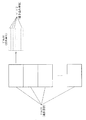
図1は、比較例としての一般的な不揮発性半導体メモリの書き込み単位と消去単位の一例を示している。図2は、比較例としての一般的な不揮発性半導体メモリにおけるデータ消去時の動作例を示している。
<0. Overview and Issues of Nonvolatile Semiconductor Memory as Comparative Example>
FIG. 1 shows an example of a writing unit and an erasing unit of a general nonvolatile semiconductor memory as a comparative example. FIG. 2 shows an operation example at the time of erasing data in a general nonvolatile semiconductor memory as a comparative example.
NAND型フラッシュメモリなどの不揮発性半導体メモリは、図1に示したように、それぞれが複数のページ2で構成された複数のブロック1を備えている。データを記憶するメモリセルは、ワード線とビット線との交点に配置される。1つのワード線上に、1または複数ページ分のデータが記憶される。データの書き込みおよび読み出しは、ページ2単位で一括して行われる。データの消去は、ブロック1単位で一括して行われる。このように、データの書き込みおよび読み出しとデータの消去は、異なる単位で行われる。このため、通常、例えば図2の上段に示したようなブロック1内の一部のページ4のデータのみを消去することはできない。一部のページ4のデータのみを消去する場合、一旦、図2の中段に示すように消去対象以外のページ2のデータをコントローラ上のRAM(Random Access Memory)や、別のブロック3などに退避する。その後、図2の下段に示すように、ブロック1全体を消去することで、一部のページ4のデータを消去する。なお、RAMに消去対象以外のページ2のデータを退避した場合、ブロック1全体を消去した後、ブロック1または別のブロック3に退避したデータを書き込む必要がある。したがって、ブロック1内の一部のデータのみを消去したい場合、有効なデータの読み出し、および書き込みを必要な回数繰り返すことになり、時間がかかる。特にブロック1が多くのページ2で構成されている場合には多くの時間が必要となる。
As shown in FIG. 1, a nonvolatile semiconductor memory such as a NAND flash memory includes a plurality of
これに対して、特許文献1(特開2014−96122号公報)では、2種類の手法が提案されている。1つは、1つのブロックに1つのファイルのみを書くことにより消去時にデータの退避が必要なくなるというものである。この手法では小さいファイルを書いた場合にはブロック内に無駄な領域が多くなるなどの問題がある。もう1つは消去対象ページにデータを上書きすることにより消去対象ページのデータを破壊してしまう方法である。消去操作が必要な不揮発性半導体メモリの書き込みはセル電位が高くなる方向にしか遷移しない。そのため、書き込み済みページにデータを上書きすると、書き込み済みのデータも上書きしたデータも読めなくなる可能性がある。 In contrast, Patent Document 1 (Japanese Patent Application Laid-Open No. 2014-96122) proposes two types of methods. One is that writing only one file in one block eliminates the need to save data during erasure. In this method, there is a problem that when a small file is written, there is a lot of wasted area in the block. The other is a method of destroying data on the page to be erased by overwriting the data on the page to be erased. Writing in a nonvolatile semiconductor memory that requires an erasing operation makes a transition only in the direction in which the cell potential increases. Therefore, if data is overwritten on a written page, there is a possibility that neither the written data nor the overwritten data can be read.
図3は、不揮発性半導体メモリにおけるカップリング現象の一例を示している。
特許文献1では、上書きするデータとしてランダムデータやセル電位が最も高くなるデータが提案されている。しかしながら、NAND型フラッシュメモリでは周辺のメモリセルの影響を受けるカップリングと呼ばれる現象がある。これは、図3に示したように、あるメモリセルと周辺の隣接するメモリセルとの電位差が大きい場合に、読み出し時において、セル電位が変化して見える現象である。例えば、図3に示したように、本来の電位よりも高い読み出し電位に変化して見える。特許文献1で提案されているデータパターンで上書きした場合、上書きしたページのメモリセルの電位が高くなり、周辺のワード線上のページ、特に前後のワード線上のページのセル電位が高く見えることがある。セル電位が高く見えると書き込み済みのデータが正しく読み出せなくなることがあり、意図しないデータ破壊につながる可能性がある。
FIG. 3 shows an example of the coupling phenomenon in the nonvolatile semiconductor memory.
<1.半導体記憶装置の一実施形態>
[1.1 構成]
図4は、本開示の一実施の形態に係る半導体記憶装置11の一例を示している。
<1. Embodiment of Semiconductor Memory Device>
[1.1 Configuration]
FIG. 4 shows an example of the semiconductor memory device 11 according to an embodiment of the present disclosure.
本実施の形態に係る半導体記憶装置11は、不揮発性半導体メモリ12と、コントローラ13と、ホストI/F(インタフェース)14とを備えている。
The semiconductor memory device 11 according to the present embodiment includes a nonvolatile semiconductor memory 12, a
不揮発性半導体メモリ12は、例えばNAND型フラッシュメモリである。不揮発性半導体メモリ12は、図1に示した比較例と略同様に、複数のページ2で構成された複数のブロック1を備えている。不揮発性半導体メモリ12の動作は、コントローラ13によって制御される。ホストI/F14は、コントローラ13とPC(パーソナルコンピュータ)などのホスト機器10とを接続するためのインタフェースである。
The nonvolatile semiconductor memory 12 is, for example, a NAND flash memory. The non-volatile semiconductor memory 12 includes a plurality of
不揮発性半導体メモリ12は、図5のようにワード線(WL)21とビット線(BL)22とが交差するマトリクス状の構成になっている。WL21とBL22との交わる部分がデータを記憶するメモリセル23となっている。選択線24は、書き込み時に各メモリセル23に書き込む値を決めるためにBL22の電圧を決定する。1つのワード線21上に、1または複数ページ分のデータが記憶される。
The nonvolatile semiconductor memory 12 has a matrix configuration in which word lines (WL) 21 and bit lines (BL) 22 intersect as shown in FIG. The intersection of WL21 and BL22 is a
メモリセル23は、例えばMLC(Multi Level Cell)やTLC(Triple Level Cell)の構成となっている。MLCの場合、1つのメモリセル23に2bit分のデータを記憶でき、1つのWL21に2ページ分のデータが記憶される。TLCの場合、1つのメモリセル23に3bit分のデータを記憶でき、1つのWL21に3ページ分のデータが記憶される。
The
[1.2 動作]
ホスト機器10が不揮発性半導体メモリ12にデータを書き込む場合、ホストI/F14を経由してコントローラ13に書き込みデータが送信される。コントローラ13は、隣接するメモリセル23とのカップリングの影響を抑えるため、線形帰還シフトレジスタ(LFSR)の出力などでスクランブルしたデータを不揮発性半導体メモリ12に書き込む。書き込む位置はコントローラ13が決定し、論物変換テーブルと呼ばれる書き込み位置の情報を保持する。
[1.2 Operation]
When the
ホスト機器10が不揮発性半導体メモリ12のデータを読み出す場合、ホストI/F14を経由してコントローラ13に読み出しアドレスが通知される。コントローラ13は論物変換テーブルを用いてデータが書き込まれている位置を取得し、不揮発性半導体メモリ12からデータを読み出し、スクランブルを解除してホストI/F14を経由してホストにデータを送信する。
When the
ホスト機器10が不揮発性半導体メモリ12のデータを消去する場合、ホストI/F14を経由してコントローラ13に消去アドレスが通知される。コントローラ13は論物変換テーブルを用いてデータが書き込まれている位置を取得する。なお、論物変換テーブルのデータを書き替えれば、通常はホスト機器10から不揮発性半導体メモリ12内のデータを読み出すことができなくなる。しかしながら、その場合でも、不揮発性半導体メモリ12内にデータが残っているため不揮発性半導体メモリ12の端子に測定器を繋ぐことによってデータが読み出される可能性がある。このため、セキュアにデータを消去するにはデータが書き込まれているページ2を消去する必要がある。コントローラ13は同じブロック1内の他のページ2に有効なデータが残っていないのを確認した場合には、そのブロック1の消去処理を行う。有効なデータが残っている場合には、消去するデータが書き込まれているページ2を、後述する所定のデータで上書きし、該当のアドレスの論物変換テーブルも削除する。
When the
以下に、データを消去する動作の具体例として、メモリセル23がMLCである場合と、メモリセル23がTLCある場合とを説明する。
Hereinafter, as a specific example of the operation of erasing data, a case where the
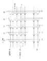
[MLCの場合の消去動作の例]
図9は、MLCのセル電位とステートおよび各ページA,Bのデータの関係の一例を示している。MLCの場合、1つのメモリセル23に2bit分のデータを記憶でき、1つのWL21に2ページ分のデータが記憶される。ここでは1つのWL21上の第1のページをページA、第2のページをページBとする。ページAに対してページBの方が上位のページとする。また、1つのメモリセル23につき、消去ステート、Aステート、Bステート、およびCステートの4段階のステートを取り得るものとする。セル電位が高い方を上位ステート、低い方を下位ステートと呼ぶ。最も下位のステートは消去ステート、最も上位のステートはCステートとなる。消去ステートとAステートとの閾値電圧をA、AステートとBステートとの閾値電圧をB、BステートとCステートとの閾値電圧をCとする。
[Example of erase operation in the case of MLC]
FIG. 9 shows an example of the relationship between the cell potential of the MLC, the state, and the data of each page A and B. In the case of MLC, data for 2 bits can be stored in one
図9のようなセル電位とステートとの関係を考慮して、一部のページ4のみを消去する場合に、コントローラ13は、消去対象の一部のページ4において、各メモリセル23にステートの変化が1段階しか起きないような所定のデータを作成して上書きする。特に、ステートの変化が下位から上位へと1段階しか起きないような所定のデータを作成して上書きする。なお、通常、書き込まれるデータはスクランブルされているため、各電圧レベルにあるメモリセル23の個数は、ブロック単位およびページ単位で大きな差はないものとする。
In consideration of the relationship between the cell potential and the state as shown in FIG. 9, when erasing only a part of the pages 4, the
図6は、MLCにおいて、ページAのみを消去する場合のメモリセル23のステートおよびデータの変化の一例を示している。コントローラ13は、消去対象の一部のページ4を含む複数のページにおける書き込み済みのデータを読み出し、その読み出しデータに基づいて、ページAに上書きする所定のデータを生成する。具体的には、コントローラ13は、ページAを消去する場合、ページAのデータとページBのデータとを読み出し、それぞれの対応するビットのデータの論理積を計算して所定のデータを生成する。その所定のデータをページAに上書きする。書き込みによりそれぞれのメモリセル23のステートは図6のように変化する。図6に示したように、ページAに所定のデータを上書き後にもページBのデータは保持される。これに対して、ページAのデータは約1/4のビットが1から0に反転するため、正しいデータが取得できなくなる。これにより、ページAのデータは実質的に消去される。また、このとき、ページA内の各メモリセル23は、ステートの変化があったとしても、1つ上のステートにしか変化しない。このため、消去対象の一部のページ4が存在するWL21に対して前後のWL21の他のページ2に書かれているデータへの影響を抑えることができる。
FIG. 6 shows an example of changes in the state and data of the
図7は、MLCにおいて、ページBのみを消去した後、ページAのみを消去する場合のメモリセル23のステートおよびデータの変化の一例を示している。ページAを消去する前に、一部のページ4としてページBのみを消去する場合には、コントローラ13は、ページB内のすべてのメモリセル23に対して、所定のデータとして、“1”のデータを上書きする。書き込みによりそれぞれのメモリセル23のステートは図7のように変化する。図7に示したように、Bステートにあったメモリセル23のみがCステートに変化するため、ページBに所定のデータを上書き後にもページAのデータは保持される。これに対して、ページBのデータは約1/4のビットが0から1に反転するため、正しいデータが取得できなくなる。これにより、ページBのデータは実質的に消去される。また、このとき、ページB内の各メモリセル23は、ステートの変化があったとしても、1つ上のステートにしか変化しない。このため、消去対象の一部のページ4が存在するWL21に対して、前後のWL21の他のページ2に書かれているデータへの影響を抑えることができる。
FIG. 7 shows an example of changes in the state and data of the
ページBを消去した後に、一部のページ4としてページAを消去する場合には、上記図6の例と同様に、ページAのデータとページBのデータとを読み出し、それぞれの対応するビットのデータの論理積を計算して所定のデータを生成する。その所定のデータをページAに上書きする。書き込みによりそれぞれのメモリセル23のステートは図7のように変化する。図7に示したように、ページAに所定のデータを上書き後にもページBのデータは保持される。これに対して、ページAのデータは約1/4のビットが1から0に反転するため、正しいデータが取得できなくなる。これにより、ページAのデータは実質的に消去される。また、このとき、ページBの消去前と比較しても、ページA内の各メモリセル23のステートの変化は、最大で1つ上のステートにしか変化しない。このため、消去対象の一部のページ4が存在するWL21に対して前後のWL21の他のページ2に書かれているデータへの影響を抑えることができる。
When erasing page A as a part of page 4 after erasing page B, the data of page A and the data of page B are read out as in the example of FIG. Predetermined data is generated by calculating the logical product of the data. The predetermined data is overwritten on page A. The state of each
図8は、MLCにおいて、ページAのみを消去した後、ページBのみを消去する場合のメモリセル23のステートおよびデータの変化の一例を示している。まず、一部のページ4として、ページAのみを消去する動作は、上記図6の例と同様である。その後、一部のページ4として、さらにページBのみを消去する場合には、コントローラ13は、ページB内のすべてのメモリセル23に対して、所定のデータとして、“0”のデータを上書きする。書き込みによりそれぞれのメモリセル23のステートは図8のように変化する。ページAを消去する前と比べると、消去ステートおよびAステートにあったメモリセル23のみが1つ上のステートに変化し、ページAおよびページBともに約1/4のビットが1から0に反転するため、正しいデータが取得できなくなる。これにより、ページAおよびページBのデータは実質的に消去される。このとき、ページAの消去前と比較しても、ページAおよびページB内の各メモリセル23のステートの変化は、最大で1つ上のステートにしか変化しない。このため、消去対象の一部のページ4が存在するWL21に対して前後のWL21の他のページ2に書かれているデータへの影響を抑えることができる。
FIG. 8 shows an example of changes in the state and data of the
[TLCの場合の消去動作の例]
図10は、TLCのセル電位とステートおよび各ページA,B,Cのデータの関係の一例を示している。TLCの場合、1つのメモリセル23に3bit分のデータを記憶でき、1つのWL21に3ページ分のデータが記憶される。ここでは1つのWL21上の第1のページをページA、第2のページをページB、第3のページをページCとする。ページAに対してページBの方が上位のページ、ページBに対してページCの方が上位のページとする。また、1つのメモリセル23につき、消去ステート、Aステート、Bステート、Cステート、Dステート、Eステート、Fステート、およびGステートの8段階のステートを取り得るものとする。セル電位が高い方を上位ステート、低い方を下位ステートと呼ぶ。最も下位のステートは消去ステート、最も上位のステートはGステートとなる。消去ステートとAステートとの閾値電圧をA、AステートとBステートとの閾値電圧をB、BステートとCステートとの閾値電圧をCとする。また、CステートとDステートとの閾値電圧をD、DステートとEステートとの閾値電圧をE、EステートとFステートとの閾値電圧をF、FステートとGステートとの閾値電圧をGとする。
[Example of erase operation in TLC]
FIG. 10 shows an example of the relationship between the cell potential of TLC, the state, and the data of each page A, B, C. In the case of TLC, data for 3 bits can be stored in one
図10のようなセル電位とステートとの関係を考慮して、一部のページ4のみを消去する場合に、コントローラ13は、消去対象の一部のページ4において、各メモリセル23にステートの変化が1段階しか起きないような所定のデータを作成または選択して上書きする。特に、ステートの変化が下位から上位へと1段階しか起きないような所定のデータを作成または選択して上書きする。上述のMLCの例とは異なり、消去するページの順番や書かれているデータに関係なく、消去対象の一部のページ4として、ページAまたはページBを消去する場合には、ページAまたはページB内のすべてのメモリセル23に対して、所定のデータとして、“1”のデータを上書きする。また、消去対象の一部のページ4として、ページCを消去する場合には、ページC内のすべてのメモリセル23に対して、所定のデータとして、“0”のデータを上書きする。それぞれの場合において、書き込みによりメモリセル23のステートは図図11〜図13のように変化する。
In consideration of the relationship between the cell potential and the state as shown in FIG. 10, when erasing only a part of the pages 4, the
図11は、TLCにおいて、ページAのみを消去する場合のメモリセル23のステートおよびデータの変化の一例を示している。図12は、TLCにおいて、ページBのみを消去する場合のメモリセル23のステートおよびデータの変化の一例を示している。図13は、TLCにおいて、ページCのみを消去する場合のメモリセル23のステートおよびデータの変化の一例を示している。
FIG. 11 shows an example of changes in the state and data of the
図11に示したように、ページAに所定のデータとして“1”のデータを上書きした場合、FステートにあったページAのメモリセル23がGステートに変化する。また、図12に示したように、ページBに所定のデータとして“1”のデータを上書きした場合、CステートにあったページBのメモリセル23がDステートに変化する。また、図13に示したように、ページCに所定のデータとして“0”のデータを上書きした場合、消去ステートにあったページCのメモリセル23がAステートに変化する。
As shown in FIG. 11, when data “1” is overwritten as predetermined data on page A, the
上記した図11〜図13のそれぞれの場合において、所定のデータを上書き後は、消去対象の一部のページ4は正しいデータが取得できなくなり、データは実質的に消去される。これに対して、消去対象以外の他の2つのページ2のデータは保持される。また、いずれの場合も、消去対象の一部のページ4内の各メモリセル23は、ステートの変化があったとしても、1つ上のステートにしか変化しない。このため、消去対象の一部のページ4が存在するWL21に対して前後のWL21の他のページ2に書かれているデータへの影響を抑えることができる。
In each case of FIGS. 11 to 13 described above, after overwriting predetermined data, a part of pages 4 to be erased cannot acquire correct data, and the data is substantially erased. On the other hand, the data of the other two
以上のように、現在のページの状態とデータの状態とにより所定のデータのデータパターンを決定し、その所定のデータを消去対象の一部のページ4に対して上書きする。これにより、高速かつ確実にデータを消去しつつ、消去対象の一部のページ4が存在するWL21に対して前後のWL21上のページ2への影響を抑えることができる。
As described above, a data pattern of predetermined data is determined based on the current page state and data state, and the predetermined data is overwritten on a part of pages 4 to be erased. Thereby, it is possible to suppress the influence on the
[1.3 効果]
以上のように、本実施の形態によれば、一部のページ4のみを消去する場合に、一部のページ4に、ステートの変化が1段階しか起きないような所定のデータを上書きするようにしたので、ブロック1内の一部のページ4のデータを安全、かつ高速に消去できる。これにより、例えば、メモリカード内のデータをセキュアに消去する必要がある場合において、高速、かつ、他のWL21におけるデータに影響を与えないように消去することが可能となる。
[1.3 Effect]
As described above, according to the present embodiment, when only some of the pages 4 are erased, the predetermined data that causes only one stage of state change is overwritten on some of the pages 4. Therefore, data of some pages 4 in the
なお、本明細書に記載された効果はあくまでも例示であって限定されるものではなく、また他の効果があってもよい。 Note that the effects described in the present specification are merely examples and are not limited, and other effects may be obtained.
<2.その他の実施の形態>
本開示による技術は、上記実施の形態の説明に限定されず種々の変形実施が可能である。
<2. Other Embodiments>
The technology according to the present disclosure is not limited to the description of the above embodiment, and various modifications can be made.
例えば、本技術は以下のような構成を取ることができる。
(1)
複数のページを有するブロックと、
データの書き込み、消去および読み出しの制御を行うコントローラと
を備え、
前記各ページは、それぞれが4段階以上のステートのうちのいずれかの段階のステートに変化し得る複数のメモリセルを有し、
前記コントローラは、前記複数のページのうち、一部のページのみを消去する場合に、前記一部のページに、前記ステートの変化が1段階しか起きないような所定のデータを上書きする
半導体記憶装置。
(2)
複数のワード線と複数のビット線とをさらに備え、
前記メモリセルは、前記複数のワード線と前記複数のビット線との交点に配置され、
前記複数のワード線のそれぞれにおいて、1つのワード線上で、複数のページ分のデータの記憶が行われる
上記(1)に記載の半導体記憶装置。
(3)
前記コントローラは、前記一部のページを含む複数のページにおける書き込み済みのデータを読み出し、その読み出しデータに基づいて、前記所定のデータを生成する
上記(1)または(2)に記載の半導体記憶装置。
(4)
前記1つのワード線上の複数のページとして、第1のページと第2のページとを含み、
前記コントローラは、前記一部のページとして前記第1のページを消去する場合には、前記第1のページ内のすべての前記メモリセルに対して、前記所定のデータとして、前記第1のページと前記第2のページとの論理積のデータを上書きする
上記(2)に記載の半導体記憶装置。
(5)
前記複数のページとして、第1のページと第2のページとを含み、
前記コントローラは、
前記第1のページを消去する前に、前記一部のページとして前記第2のページを消去する場合には、前記第2のページ内のすべての前記メモリセルに対して、前記所定のデータとして、“1”のデータを上書きし、
前記第2のページを消去した後に、前記一部のページとして、さらに前記第1のページを消去する場合には、前記第1のページ内のすべての前記メモリセルに対して、前記所定のデータとして、前記第1のページと前記第2のページとの論理積のデータを上書きする
上記(2)に記載の半導体記憶装置。
(6)
前記複数のページとして、第1のページと第2のページとを含み、
前記コントローラは、
前記一部のページとして前記第1のページを消去する場合には、前記第1のページ内のすべての前記メモリセルに対して、前記所定のデータとして、前記第1のページと前記第2のページとの論理積のデータを上書きし、
その後、前記一部のページとして、さらに前記第2のページを消去する場合には、前記第2のページ内のすべての前記メモリセルに対して、前記所定のデータとして、“0”のデータを上書きする
上記(2)に記載の半導体記憶装置。
(7)
前記メモリセルは、4段階のステートに変化し得る
上記(1)ないし(6)のいずれか1つに記載の半導体記憶装置。
(8)
前記1つのワード線上の複数のページとして、第1ないし第3のページを含み、
前記コントローラは、
前記一部のページとして、前記第1のページまたは前記第2のページを消去する場合には、前記第1のページ内のすべてのメモリセルまたは前記第2のページ内のすべての前記メモリセルに対して、前記所定のデータとして、“1”のデータを上書きし、
前記一部のページとして、前記第3のページを消去する場合には、前記第3のページ内のすべての前記メモリセルに対して、前記所定のデータとして、“0”のデータを上書きする
上記(2)に記載の半導体記憶装置。
(9)
前記メモリセルは、8段階のステートに変化し得る
上記(8)に記載の半導体記憶装置。
(10)
複数のページを有するブロックを備え、前記各ページが、それぞれ4段階以上のステートのうちのいずれかの段階のステートになり得る複数のメモリセルを有する半導体記憶装置に対して、
前記複数のページのうち、一部のページのみを消去する場合に、前記一部のページに、前記ステートの変化が1段階しか起きないような所定のデータを上書きする
半導体記憶装置におけるデータ消去方法。
For example, the present technology can take the following configurations.
(1)
A block having a plurality of pages;
And a controller for controlling writing, erasing and reading of data,
Each page includes a plurality of memory cells, each of which can change to any one of four or more states.
The controller, when erasing only a part of the plurality of pages, overwrites the part of the page with predetermined data such that the state change occurs only in one stage. Semiconductor memory device .
(2)
A plurality of word lines and a plurality of bit lines;
The memory cell is disposed at an intersection of the plurality of word lines and the plurality of bit lines,
In each of the plurality of word lines, the data for a plurality of pages is stored on one word line. The semiconductor memory device according to (1) above.
(3)
The semiconductor memory device according to (1) or (2), wherein the controller reads written data in a plurality of pages including the partial page, and generates the predetermined data based on the read data .
(4)
A plurality of pages on the one word line including a first page and a second page;
When erasing the first page as the partial page, the controller sets the first page as the predetermined data for all the memory cells in the first page. The semiconductor memory device according to (2), wherein data of a logical product with the second page is overwritten.
(5)
The plurality of pages includes a first page and a second page,
The controller is
When erasing the second page as the partial page before erasing the first page, the predetermined data is used as the predetermined data for all the memory cells in the second page. , Overwrite the data of “1”,
When the first page is further erased as the partial page after erasing the second page, the predetermined data is stored in all the memory cells in the first page. As described above, the data of the logical product of the first page and the second page is overwritten.
(6)
The plurality of pages includes a first page and a second page,
The controller is
When erasing the first page as the partial page, the first page and the second page are used as the predetermined data for all the memory cells in the first page. Overwrite the logical product with the page,
Thereafter, when erasing the second page as the partial page, data “0” is set as the predetermined data for all the memory cells in the second page. The semiconductor memory device according to (2), which is overwritten.
(7)
The semiconductor memory device according to any one of (1) to (6), wherein the memory cell can change to a four-stage state.
(8)
The plurality of pages on the one word line include first to third pages,
The controller is
When erasing the first page or the second page as the partial page, all the memory cells in the first page or all the memory cells in the second page On the other hand, “1” data is overwritten as the predetermined data,
When erasing the third page as the partial page, data “0” is overwritten as the predetermined data in all the memory cells in the third page. The semiconductor memory device according to (2).
(9)
The semiconductor memory device according to (8), wherein the memory cell can change to eight states.
(10)
A semiconductor memory device comprising a block having a plurality of pages, and each page having a plurality of memory cells each of which can be in any one of four or more stages.
A method of erasing data in a semiconductor memory device, wherein only a part of the plurality of pages is erased by overwriting predetermined data in which the state change occurs only in one stage. .
1…ブロック、2…ページ、3…ブロック、4…ページ、10…ホスト機器、11…半導体記憶装置、12…不揮発性半導体メモリ、13…コントローラ、14…ホストI/F(インタフェース)、21…ワード線(WL)、22…ビット線(BL)、23…メモリセル、24…選択線。
DESCRIPTION OF
Claims (10)
データの書き込み、消去および読み出しの制御を行うコントローラと
を備え、
前記各ページは、それぞれが4段階以上のステートのうちのいずれかの段階のステートに変化し得る複数のメモリセルを有し、
前記コントローラは、前記複数のページのうち、一部のページのみを消去する場合に、前記一部のページに、前記ステートの変化が1段階しか起きないような所定のデータを上書きする
半導体記憶装置。 A block having a plurality of pages;
And a controller for controlling writing, erasing and reading of data,
Each page includes a plurality of memory cells, each of which can change to any one of four or more states.
The controller, when erasing only a part of the plurality of pages, overwrites the part of the page with predetermined data such that the state change occurs only in one stage. Semiconductor memory device .
前記メモリセルは、前記複数のワード線と前記複数のビット線との交点に配置され、
前記複数のワード線のそれぞれにおいて、1つのワード線上で、複数のページ分のデータの記憶が行われる
請求項1に記載の半導体記憶装置。 A plurality of word lines and a plurality of bit lines;
The memory cell is disposed at an intersection of the plurality of word lines and the plurality of bit lines,
The semiconductor memory device according to claim 1, wherein in each of the plurality of word lines, data for a plurality of pages is stored on one word line.
請求項1に記載の半導体記憶装置。 The semiconductor memory device according to claim 1, wherein the controller reads written data in a plurality of pages including the some pages, and generates the predetermined data based on the read data.
前記コントローラは、前記一部のページとして前記第1のページを消去する場合には、前記第1のページ内のすべての前記メモリセルに対して、前記所定のデータとして、前記第1のページと前記第2のページとの論理積のデータを上書きする
請求項2に記載の半導体記憶装置。 A plurality of pages on the one word line including a first page and a second page;
When erasing the first page as the partial page, the controller sets the first page as the predetermined data for all the memory cells in the first page. The semiconductor memory device according to claim 2, wherein data of a logical product with the second page is overwritten.
前記コントローラは、
前記第1のページを消去する前に、前記一部のページとして前記第2のページを消去する場合には、前記第2のページ内のすべての前記メモリセルに対して、前記所定のデータとして、“1”のデータを上書きし、
前記第2のページを消去した後に、前記一部のページとして、さらに前記第1のページを消去する場合には、前記第1のページ内のすべての前記メモリセルに対して、前記所定のデータとして、前記第1のページと前記第2のページとの論理積のデータを上書きする
請求項2に記載の半導体記憶装置。 The plurality of pages includes a first page and a second page,
The controller is
When erasing the second page as the partial page before erasing the first page, the predetermined data is used as the predetermined data for all the memory cells in the second page. , Overwrite the data of “1”,
When the first page is further erased as the partial page after erasing the second page, the predetermined data is stored in all the memory cells in the first page. The semiconductor memory device according to claim 2, wherein data of a logical product of the first page and the second page is overwritten.
前記コントローラは、
前記一部のページとして前記第1のページを消去する場合には、前記第1のページ内のすべての前記メモリセルに対して、前記所定のデータとして、前記第1のページと前記第2のページとの論理積のデータを上書きし、
その後、前記一部のページとして、さらに前記第2のページを消去する場合には、前記第2のページ内のすべての前記メモリセルに対して、前記所定のデータとして、“0”のデータを上書きする
請求項2に記載の半導体記憶装置。 The plurality of pages includes a first page and a second page,
The controller is
When erasing the first page as the partial page, the first page and the second page are used as the predetermined data for all the memory cells in the first page. Overwrite the logical product with the page,
Thereafter, when erasing the second page as the partial page, data “0” is set as the predetermined data for all the memory cells in the second page. The semiconductor memory device according to claim 2, wherein overwriting is performed.
請求項1に記載の半導体記憶装置。 The semiconductor memory device according to claim 1, wherein the memory cell can change into four stages.
前記コントローラは、
前記一部のページとして、前記第1のページまたは前記第2のページを消去する場合には、前記第1のページ内のすべてのメモリセルまたは前記第2のページ内のすべての前記メモリセルに対して、前記所定のデータとして、“1”のデータを上書きし、
前記一部のページとして、前記第3のページを消去する場合には、前記第3のページ内のすべての前記メモリセルに対して、前記所定のデータとして、“0”のデータを上書きする
請求項2に記載の半導体記憶装置。 The plurality of pages on the one word line include first to third pages,
The controller is
When erasing the first page or the second page as the partial page, all the memory cells in the first page or all the memory cells in the second page On the other hand, “1” data is overwritten as the predetermined data,
When erasing the third page as the partial page, data of “0” is overwritten as the predetermined data in all the memory cells in the third page. Item 3. The semiconductor memory device according to Item 2.
請求項8に記載の半導体記憶装置。 The semiconductor memory device according to claim 8, wherein the memory cell can change to an eight-stage state.
前記複数のページのうち、一部のページのみを消去する場合に、前記一部のページに、前記ステートの変化が1段階しか起きないような所定のデータを上書きする
半導体記憶装置におけるデータ消去方法。 A semiconductor memory device comprising a block having a plurality of pages, and each page having a plurality of memory cells each of which can be in any one of four or more stages.
A method of erasing data in a semiconductor memory device, wherein only a part of the plurality of pages is erased by overwriting predetermined data in which the state change occurs only in one stage. .
Priority Applications (3)
| Application Number | Priority Date | Filing Date | Title |
|---|---|---|---|
| JP2015181628A JP2017059281A (en) | 2015-09-15 | 2015-09-15 | Semiconductor storage device and data erasing method for semiconductor storage device |
| US15/758,021 US10658042B2 (en) | 2015-09-15 | 2016-08-04 | Semiconductor memory device and method of erasing data of partial page and overwriting partial page with predetermined data |
| PCT/JP2016/072919 WO2017047272A1 (en) | 2015-09-15 | 2016-08-04 | Semiconductor storage device and data erasure method in semiconductor storage device |
Applications Claiming Priority (1)
| Application Number | Priority Date | Filing Date | Title |
|---|---|---|---|
| JP2015181628A JP2017059281A (en) | 2015-09-15 | 2015-09-15 | Semiconductor storage device and data erasing method for semiconductor storage device |
Publications (2)
| Publication Number | Publication Date |
|---|---|
| JP2017059281A true JP2017059281A (en) | 2017-03-23 |
| JP2017059281A5 JP2017059281A5 (en) | 2018-10-18 |
Family
ID=58288872
Family Applications (1)
| Application Number | Title | Priority Date | Filing Date |
|---|---|---|---|
| JP2015181628A Ceased JP2017059281A (en) | 2015-09-15 | 2015-09-15 | Semiconductor storage device and data erasing method for semiconductor storage device |
Country Status (3)
| Country | Link |
|---|---|
| US (1) | US10658042B2 (en) |
| JP (1) | JP2017059281A (en) |
| WO (1) | WO2017047272A1 (en) |
Cited By (1)
| Publication number | Priority date | Publication date | Assignee | Title |
|---|---|---|---|---|
| US10685713B2 (en) | 2018-04-25 | 2020-06-16 | Samsung Electronics Co., Ltd. | Storage device including nonvolatile memory device and controller |
Families Citing this family (1)
| Publication number | Priority date | Publication date | Assignee | Title |
|---|---|---|---|---|
| GB2620445A (en) * | 2022-07-08 | 2024-01-10 | Kirintec Ltd | Data erasure system |
Family Cites Families (5)
| Publication number | Priority date | Publication date | Assignee | Title |
|---|---|---|---|---|
| US7580151B2 (en) * | 2003-10-01 | 2009-08-25 | Seiko Epson Corporation | Image processing system and method, printing system |
| KR20140021780A (en) * | 2012-08-10 | 2014-02-20 | 삼성전자주식회사 | Nonvolatile memory device and control method thereof |
| JP2014096122A (en) | 2012-11-12 | 2014-05-22 | Genusion:Kk | File recording method for storage medium using nonvolatile semiconductor memory device |
| US9098401B2 (en) * | 2012-11-21 | 2015-08-04 | Apple Inc. | Fast secure erasure schemes for non-volatile memory |
| US20160155495A1 (en) * | 2013-07-08 | 2016-06-02 | Wilus Institute Of Standards And Technology Inc. | Memory system and method for processing data in memory |
-
2015
- 2015-09-15 JP JP2015181628A patent/JP2017059281A/en not_active Ceased
-
2016
- 2016-08-04 US US15/758,021 patent/US10658042B2/en active Active
- 2016-08-04 WO PCT/JP2016/072919 patent/WO2017047272A1/en active Application Filing
Cited By (1)
| Publication number | Priority date | Publication date | Assignee | Title |
|---|---|---|---|---|
| US10685713B2 (en) | 2018-04-25 | 2020-06-16 | Samsung Electronics Co., Ltd. | Storage device including nonvolatile memory device and controller |
Also Published As
| Publication number | Publication date |
|---|---|
| US10658042B2 (en) | 2020-05-19 |
| WO2017047272A1 (en) | 2017-03-23 |
| US20180254088A1 (en) | 2018-09-06 |
Similar Documents
| Publication | Publication Date | Title |
|---|---|---|
| KR102190694B1 (en) | Nonvolatile memory system and operating method thereof | |
| US9575839B2 (en) | Data storage device and operating method thereof | |
| JP5497754B2 (en) | Ad hoc flash memory reference cell | |
| US10168913B2 (en) | Data storage device and data maintenance method thereof | |
| CN106558330B (en) | Semiconductor device, method of operating the same, and data storage apparatus including the same | |
| JP2005108303A (en) | Nonvolatile semiconductor memory | |
| US10241678B2 (en) | Data storage device and data writing method capable of avoiding repeated write operation of a TLC block when interrupted | |
| US9520184B2 (en) | Method for writing in-system programming code into flash memory for better noise margin | |
| US9940058B2 (en) | Data storage device and data maintenance method thereof | |
| US10013210B2 (en) | Data storage device and data maintenance method thereof | |
| KR102592796B1 (en) | Data storage device and operating method thereof | |
| US10168951B2 (en) | Methods for accessing data in a circular block mode and apparatuses using the same | |
| US20080288743A1 (en) | Apparatus and method of managing mapping table of non-volatile memory | |
| CN101796498B (en) | Memory system | |
| KR20200034189A (en) | Memory system, operating method thereof and non-volatile memory device | |
| US20170285953A1 (en) | Data Storage Device and Data Maintenance Method thereof | |
| US20150089119A1 (en) | Command execution using existing address information | |
| WO2017047272A1 (en) | Semiconductor storage device and data erasure method in semiconductor storage device | |
| KR100967026B1 (en) | Non volatile memory device and cache reading method thereof | |
| US20160372169A1 (en) | Memory devices with improved refreshing operation | |
| KR20210080987A (en) | Memory device and operation method thereof | |
| JP2015103093A (en) | Flash memory, bad block management method, and management program | |
| US10902922B2 (en) | Nonvolatile memory device storing data in sub-blocks and operating method thereof | |
| JP2005339438A (en) | Memory controller, flash memory system and control method of flash memory | |
| US20230031193A1 (en) | Memory system and operating method thereof |
Legal Events
| Date | Code | Title | Description |
|---|---|---|---|
| A521 | Written amendment |
Free format text: JAPANESE INTERMEDIATE CODE: A523 Effective date: 20180910 |
|
| A621 | Written request for application examination |
Free format text: JAPANESE INTERMEDIATE CODE: A621 Effective date: 20180910 |
|
| A131 | Notification of reasons for refusal |
Free format text: JAPANESE INTERMEDIATE CODE: A131 Effective date: 20190528 |
|
| A521 | Written amendment |
Free format text: JAPANESE INTERMEDIATE CODE: A523 Effective date: 20190718 |
|
| A131 | Notification of reasons for refusal |
Free format text: JAPANESE INTERMEDIATE CODE: A131 Effective date: 20191015 |
|
| A521 | Written amendment |
Free format text: JAPANESE INTERMEDIATE CODE: A523 Effective date: 20191118 |
|
| A01 | Written decision to grant a patent or to grant a registration (utility model) |
Free format text: JAPANESE INTERMEDIATE CODE: A01 Effective date: 20200428 |
|
| A045 | Written measure of dismissal of application [lapsed due to lack of payment] |
Free format text: JAPANESE INTERMEDIATE CODE: A045 Effective date: 20200929 |