JP2017037699A - Multi-sensor reader, reader, and method of forming multi-sensor reader - Google Patents
Multi-sensor reader, reader, and method of forming multi-sensor reader Download PDFInfo
- Publication number
- JP2017037699A JP2017037699A JP2016105076A JP2016105076A JP2017037699A JP 2017037699 A JP2017037699 A JP 2017037699A JP 2016105076 A JP2016105076 A JP 2016105076A JP 2016105076 A JP2016105076 A JP 2016105076A JP 2017037699 A JP2017037699 A JP 2017037699A
- Authority
- JP
- Japan
- Prior art keywords
- sensor
- reader
- layer
- shielding element
- saf
- Prior art date
- Legal status (The legal status is an assumption and is not a legal conclusion. Google has not performed a legal analysis and makes no representation as to the accuracy of the status listed.)
- Pending
Links
Images


Classifications
-
- G—PHYSICS
- G11—INFORMATION STORAGE
- G11B—INFORMATION STORAGE BASED ON RELATIVE MOVEMENT BETWEEN RECORD CARRIER AND TRANSDUCER
- G11B5/00—Recording by magnetisation or demagnetisation of a record carrier; Reproducing by magnetic means; Record carriers therefor
- G11B5/127—Structure or manufacture of heads, e.g. inductive
- G11B5/33—Structure or manufacture of flux-sensitive heads, i.e. for reproduction only; Combination of such heads with means for recording or erasing only
- G11B5/39—Structure or manufacture of flux-sensitive heads, i.e. for reproduction only; Combination of such heads with means for recording or erasing only using magneto-resistive devices or effects
- G11B5/3903—Structure or manufacture of flux-sensitive heads, i.e. for reproduction only; Combination of such heads with means for recording or erasing only using magneto-resistive devices or effects using magnetic thin film layers or their effects, the films being part of integrated structures
- G11B5/3906—Details related to the use of magnetic thin film layers or to their effects
- G11B5/3912—Arrangements in which the active read-out elements are transducing in association with active magnetic shields, e.g. magnetically coupled shields
-
- G—PHYSICS
- G11—INFORMATION STORAGE
- G11B—INFORMATION STORAGE BASED ON RELATIVE MOVEMENT BETWEEN RECORD CARRIER AND TRANSDUCER
- G11B5/00—Recording by magnetisation or demagnetisation of a record carrier; Reproducing by magnetic means; Record carriers therefor
- G11B5/127—Structure or manufacture of heads, e.g. inductive
- G11B5/33—Structure or manufacture of flux-sensitive heads, i.e. for reproduction only; Combination of such heads with means for recording or erasing only
- G11B5/39—Structure or manufacture of flux-sensitive heads, i.e. for reproduction only; Combination of such heads with means for recording or erasing only using magneto-resistive devices or effects
- G11B5/3903—Structure or manufacture of flux-sensitive heads, i.e. for reproduction only; Combination of such heads with means for recording or erasing only using magneto-resistive devices or effects using magnetic thin film layers or their effects, the films being part of integrated structures
- G11B5/3906—Details related to the use of magnetic thin film layers or to their effects
- G11B5/3945—Heads comprising more than one sensitive element
- G11B5/3948—Heads comprising more than one sensitive element the sensitive elements being active read-out elements
-
- G—PHYSICS
- G11—INFORMATION STORAGE
- G11B—INFORMATION STORAGE BASED ON RELATIVE MOVEMENT BETWEEN RECORD CARRIER AND TRANSDUCER
- G11B5/00—Recording by magnetisation or demagnetisation of a record carrier; Reproducing by magnetic means; Record carriers therefor
- G11B5/127—Structure or manufacture of heads, e.g. inductive
- G11B5/33—Structure or manufacture of flux-sensitive heads, i.e. for reproduction only; Combination of such heads with means for recording or erasing only
- G11B5/39—Structure or manufacture of flux-sensitive heads, i.e. for reproduction only; Combination of such heads with means for recording or erasing only using magneto-resistive devices or effects
- G11B5/3903—Structure or manufacture of flux-sensitive heads, i.e. for reproduction only; Combination of such heads with means for recording or erasing only using magneto-resistive devices or effects using magnetic thin film layers or their effects, the films being part of integrated structures
- G11B5/3967—Composite structural arrangements of transducers, e.g. inductive write and magnetoresistive read
- G11B5/397—Composite structural arrangements of transducers, e.g. inductive write and magnetoresistive read with a plurality of independent magnetoresistive active read-out elements for respectively transducing from selected components
Abstract
Description
背景
データ記憶装置は一般的に、データ記憶媒体から情報を読取る読取トランスデューサと、データ記憶媒体に情報を書込む書込トランスデューサとを含む記録ヘッドを有する。
BACKGROUND Data storage devices typically have a recording head that includes a read transducer that reads information from the data storage medium and a write transducer that writes information to the data storage medium.
ディスクドライブなどの磁気データ記憶装置では、磁気媒体から磁気信号を読取る読取トランスデューサとして、巨大磁気抵抗(GMR)センサまたはトンネル接合磁気抵抗(TMR)センサなどの磁気抵抗(MR)センサを用いることがある。MRセンサは外部磁界に応答して変化する電気抵抗を有する。隣接する磁気媒体から磁気データを読取るために、この電気抵抗の変化を処理回路構成によって検出することができる。 In a magnetic data storage device such as a disk drive, a magnetoresistive (MR) sensor such as a giant magnetoresistive (GMR) sensor or a tunnel junction magnetoresistive (TMR) sensor may be used as a read transducer that reads a magnetic signal from a magnetic medium. . MR sensors have an electrical resistance that changes in response to an external magnetic field. In order to read magnetic data from adjacent magnetic media, this change in electrical resistance can be detected by the processing circuitry.
高くなり続けるディスクドライブ中の記録密度のレベルおよびより速いデータ転送速度に対する必要性とともに、読取トランスデューサは対応してより高いデータ再生能力を有する必要がある。 Along with the need for higher recording density levels in disk drives and higher data transfer rates, read transducers must correspondingly have higher data playback capabilities.
要約
本開示は、センサ同士の間の間隔を縮小する少なくとも1つの特徴を含むことによって、より高いデータ密度要件とデータトラックに対するヘッドスキューとによって提起される課題に対処するマルチセンサ読取器に関する。マルチセンサ読取器は、外部磁界に応じて変化する磁性を有するフリー層(FL)を含むセンサ積層体を有する第1のセンサを含む。第1のセンサは、センサ積層体の上に位置決めされる遮蔽構造も含む。マルチセンサ読取器は、第1のセンサ上に積層される第2のセンサも含む。第2のセンサは、外部磁界に応じて変化する磁性を有するFLを含むセンサ積層体を含む。マルチセンサ読取器はさらに、第1のセンサと第2のセンサとの間の分離層を含む。分離層および遮蔽構造の少なくとも1つの中に、FL−FL間隔縮小特徴が含まれる。
SUMMARY The present disclosure relates to a multi-sensor reader that addresses the challenges posed by higher data density requirements and head skew to data tracks by including at least one feature that reduces the spacing between sensors. The multi-sensor reader includes a first sensor having a sensor stack including a free layer (FL) having magnetism that changes in response to an external magnetic field. The first sensor also includes a shielding structure positioned on the sensor stack. The multi-sensor reader also includes a second sensor stacked on the first sensor. The second sensor includes a sensor stack including a FL having magnetism that changes in response to an external magnetic field. The multi-sensor reader further includes a separation layer between the first sensor and the second sensor. FL-FL spacing reduction features are included in at least one of the separation layer and the shielding structure.
開示の実施形態を特徴付ける他の特徴および利点は、以下の詳細な説明を読みかつ関連の図面を検討することから明らかになるであろう。 Other features and advantages that characterize the disclosed embodiments will be apparent from a reading of the following detailed description and a review of the associated drawings.
例示的な実施形態の詳細な説明
以下に記載する磁気再生装置実施形態は、センサ同士の間の間隔を縮小する少なくとも1つの特徴を含むマルチセンサ読取器に関する。しかしながら、異なる実施形態に関する付加的な詳細を与える前に、例示的な動作環境の説明を以下に提供する。
Detailed Description of Exemplary Embodiments The magnetic regenerator embodiments described below relate to a multi-sensor reader that includes at least one feature that reduces the spacing between sensors. However, prior to providing additional details regarding the different embodiments, a description of an exemplary operating environment is provided below.
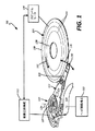
図1は、本明細書中に開示されるある具体的な実施形態を組入れ得る例示的な動作環境を示す。図1に示される動作環境は例示の目的のためのみのものである。本開示の実施形態は図1に示される動作環境などの一切の特定の動作環境に限定されない。本開示の実施形態は任意の数の異なる種類の動作環境内で例示的に実践される。同じ参照番号が同じまたは類似の要素について異なる図中で用いられることに留意すべきである。 FIG. 1 illustrates an exemplary operating environment in which certain specific embodiments disclosed herein may be incorporated. The operating environment shown in FIG. 1 is for illustrative purposes only. Embodiments of the present disclosure are not limited to any particular operating environment, such as the operating environment shown in FIG. Embodiments of the present disclosure are exemplarily practiced in any number of different types of operating environments. It should be noted that the same reference numerals are used in different figures for the same or similar elements.
図1は、データ記憶媒体と、データ記憶媒体からデータを読取るおよび/またはデータ記憶媒体にデータを書込むためのヘッドとを含むデータ記憶装置100の概略図である。データ記憶装置100では、ヘッド102が記憶媒体104の上に位置決めされてデータ記憶媒体104からデータを読取るおよび/またはデータ記憶媒体104にデータを書込む。示される実施形態では、データ記憶媒体104は、1つの磁気記憶層または複数の磁気記憶層を含む回転可能なディスクまたは他の磁気記憶媒体である。読取および書込動作のため、(概略的に図示される)スピンドルモータ106は、矢印107で示されるように媒体104を回転させ、アクチュエータ機構110は、内径108と外径109との間の、回転する媒体104上のデータトラック114に対してヘッド102を位置決めする。スピンドルモータ106およびアクチュエータ機構110の両方ともが(概略的に示される)駆動回路構成112に接続されかつこれによって動作される。ヘッド102は、たとえばスエージ加工接続を通して機構110のアクチュエータアーム122に接続されるロードビーム120を含む懸架アセンブリを通してアクチュエータ機構110に結合される。図1は単一のロードビームがアクチュエータ機構110に結合されているのを示すが、付加的なロードビーム120およびヘッド102をアクチュエータ機構110に結合してディスク積層体の複数のディスクからデータを読取ったりそこにデータを書込んだりすることができる。アクチュエータ機構110は、軸受124を通してフレームまたはデッキ(図示せず)に回転するように結合されて軸126の周りを回転する。アクチュエータ機構110の回転は、矢印130で示されるように、トラック横断方向にヘッド102を移動させる。
FIG. 1 is a schematic diagram of a
ヘッド102は、屈曲回路134を通してヘッド回路構成132に結合される(図1には示さない)1つ以上のトランスデューサ要素を含む。102などのヘッドの要素に関する詳細は、図2に関連して以下に与えられる。
The
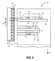
図2は、記録ヘッド200の担持面(たとえば、空気担持面(ABS))202の平面に対して実質的に法線方向の平面に沿った、記録ヘッド200およびデータ記憶媒体250の一部の断面図を示す概略図である。図2に示される記録ヘッド要素は例示的には、図1の記録ヘッド102などの記録ヘッド中に含まれる。媒体250は例示的には図1の媒体104などのデータ記憶媒体である。当業者は、記録ヘッドおよび記録媒体が一般的に他の構成要素を含むことを認識するであろう。本開示の実施形態は一切の特定の記録ヘッドまたは媒体に限定されない。本開示の実施形態を異なる種類の記録ヘッドおよび媒体において実践してもよい。
FIG. 2 illustrates a portion of the
記録ヘッド200は、書込極205、磁化コイル210、帰還極215、頂部シールド218、読取トランスデューサ220、底部シールド222、およびウェハ保護膜224を含む。記憶媒体250は、記録層255および下地層260を含む。記憶媒体250は矢印265で示される方向に回転する。矢印265は例示的に図1の矢印107などの回転の方向である。
The
ある実施形態では、電流がコイル210を通過して磁界を生成する。磁界は、書込極205から記録層255を通って下地層260の中に入り、次に横断して帰還極215へと通っていく。磁界は例示的には、記録層255中の磁化パターン270を記録する。読取トランスデューサ220は、記録層255中の磁化パターンを検知または検出し、先に層255に記録された情報を取出すのに用いられる。
In some embodiments, current passes through
より高いデータ密度要件およびより速いデータ転送速度によって提起される課題に対処するため、読取トランスデューサ220は複数のセンサ226および228を含む。簡略のため、図2に示されるのはセンサ226および228の2つのみであることに留意すべきである。しかしながら、異なるマルチセンサ読取器実施形態では、任意の好適な数のセンサが用いられることがある。異なるマルチセンサ読取器実施形態では、磁気センサは、トラック方向(すなわち、図2のz方向)またはトラック方向に垂直なトラック幅方向(すなわち、図2のx方向であるトラック横断方向)に沿って積層されてもよい。そして図2のy方向は、ストライプ高さ方向である、同時にxおよびzに垂直な方向として定義される。図2に示される実施形態では、センサ226および228はトラック方向に沿って積層される。そのような実施形態では、高いデータ記憶密度を達成するために、またデータトラックに対するヘッドスキューにより、隣接するセンサ226および228の主な検知構成要素同士の間の間隔を小さくすることが望ましい。ヘッドスキューは回転アクチュエータの当然の結果であるが、これは、完全に径方向にトラックを横切るようにヘッドを移動させず、大抵はディスクの内径および外径の近くで顕著である(図1を参照)。図2の実施形態では、読取トランスデューサ220は少なくとも1つの厚み/間隔縮小特徴230を含む。個々のセンサの実施形態の異なる層を図3Aに示し、図3Bは、図3Aに示される種類のセンサを2つ含むマルチセンサ読取器を示す。マルチセンサ読取器中のセンサ間の間隔縮小に関する詳細は、図4−図11に関連して以下にさらに与えられる。
To address the challenges posed by higher data density requirements and higher data rates, read
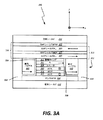
図3Aは、単一の磁気抵抗センサ302を含む例示的な読取ヘッド300を示す概略ブロック図である。磁気抵抗センサ302は、頂部シールド218と底部シールド222との間に位置決めされる。高い透磁性を有する材料から作られ得る頂部および底部シールド218および222は、たとえばデータディスク上の隣接するビットからの磁界などの外部磁界が磁気抵抗センサ302に影響を与えるのを低減するかまたは実質的にブロックして、こうして磁気抵抗センサ302の性能を向上させる。1つの実現例では、頂部および底部シールド218および222は、磁気抵抗センサ302の直下のビットからの磁界が磁気抵抗センサ302に影響を及ぼして読取られるようにする。
FIG. 3A is a schematic block diagram illustrating an
磁気抵抗センサ302は、センサ反強磁性(AFM)層304、センサ積層合成反強磁性(SAF)構造306、スペーサ層308、フリー層または検知層310、積層キャップ312、およびSAF遮蔽構造314を含む複数の層を含む。
The
図3Aに示される実施形態では、センサSAF構造306は、ピンド層316、ある実施形態ではルテニウム(Ru)などの金属を備え得る薄い隔離層318、および参照層320を含む。ピンド層316および参照層320の各々の磁気モーメントは、対象の範囲中の磁界(たとえば、データディスク上に記憶されるデータのビットによって生成される磁界)の下で回転することを許容されない。参照層320およびピンド層316の磁気モーメントは一般的に、図3Aの平面(すなわちy方向)に対して法線方向にかつ互いに逆平行に向けられる。
In the embodiment shown in FIG. 3A, the
1つの実現例では、フリー層310はたとえば反強磁性体に交換結合されない。その結果、フリー層310の磁気モーメントは、対象の範囲中の印加される磁界の影響下で自由に回転する。読取ヘッド300はさらに、側方バイアス磁石または側方シールド322を含み、これらは紙面に平行でありかつほぼ水平に向けられる磁気モーメントでフリー層310をバイアスする磁界を発生する。このバイアスは、読取ヘッド300によって検知されるデータの中にノイズを導入することがあるたとえば熱エネルギによってフリー層310の磁気モーメントがドリフトするのを防止する。バイアスは十分に小さいが、フリー層310の磁気モーメントは、データディスク上に記憶されるデータビットの磁界などの印加磁界に応答して変化する可能性がある。ある実施形態では、側方バイアス磁石または側方シールド322は、軟磁性材料(すなわち、相対的に低い磁界で容易に磁化されかつ消磁されることができる材料)から形成される。軟磁性材料は、NiおよびFeを備える合金であり得る。磁気抵抗センサ302は、たとえば絶縁材料を含む分離層324によって側方バイアス磁石322から隔離されかつ電気的に分離される。図3Aに示されるように、分離層324はヘッド300の他の領域にも存在してもよい。
In one implementation, the
図3Aに示される実施形態では、SAF遮蔽構造は、SAFシールド参照層326、ある実施形態ではRuなどの金属を備え得る薄いSAFシールド隔離層328、SAFシールドピンド層330、およびSAFシールドAFM層332を含む。センサ300は軟磁性側方シールド322を利用するので、側方シールド322の磁化を安定化させるのを助けるには、SAFシールド参照層326は、相対的に固定された磁性を有する必要がある。このように、AFM層332は担持面に実質的に平行な層SAFシールドピンド層330の磁化をピン止めする必要があり、この結果、SAFシールド隔離層328を横切る反強磁性結合によるSAFシールド参照層326の相対的に固定された磁化、およびしたがって担持面に実質的に平行な側方シールド322の磁化の安定も生じさせる。SAFシールド参照層326およびSAFシールドピンド層330は軟磁性材料(たとえば、NiおよびFeを備える合金)から形成されてもよい。ある実施形態では、SAFシールドAFM332と頂部シールド218との間、およびセンサAFM304と底部シールド222との間に非磁性金属インサート(図示せず)が存在してもよいことに留意すべきである。
In the embodiment shown in FIG. 3A, the SAF shielding structure includes a SAF
ある実施形態では、センサ302は、トンネル磁気抵抗(TMR)または巨大磁気抵抗(GMR)効果を利用してもよい。TMR効果を利用する実施形態では、スペーサ層308は、SAF構造306をフリー層310から隔離するトンネルバリア層である。トンネルバリア層308は十分に薄いので、SAF構造306中の参照層320とフリー層310との間に量子力学的電子トンネリングが起こる。電子トンネリングは電子スピンに依存し、磁気抵抗センサ302の磁気応答をSAF構造306およびフリー層310の相対的な向きおよびスピン偏極の関数にする。電子トンネリングの最も高い可能性は、SAF構造306とフリー層310との磁気モーメントが平行であるときに起こり、電子トンネリングの最も低い可能性は、SAF構造306とフリー層310との磁気モーメントが逆平行であるときに起こる。したがって、磁気抵抗センサ302の電気抵抗は、印加される磁界に応答して変化する。ディスクドライブ中のデータディスク上のデータビットは、図3Aの紙面に対して法線方向に、紙面の中または紙面から外のいずれかへ磁化され得る。このように、磁気抵抗センサ302がデータビットの上を通過すると、フリー層310の磁気モーメントは図3Aの紙面の中へまたは図3Aの紙面から外へ回転されて、磁気抵抗センサ302の電気抵抗を変化させる。したがって、磁気抵抗センサ302によって検知されるビットの値(たとえば、1または0)は、第1の電極(図示せず)から磁気抵抗センサ302に接続される第2の電極(図示せず)に流れる電流に基づいて決まり得る。
In some embodiments, the
図3Bは、トラック方向(すなわち図3Bのz方向)に沿って積層される複数の磁気抵抗センサ(たとえば、302Aおよび302B)を含む例示的な読取ヘッド350を示す概略ブロック図である。センサ302Aおよび302Bの各々は図3Aのセンサ302と実質的に同様であり、したがって、個々のセンサ302Aおよび302Bの説明は図3Bに関連しては与えられない。データ記憶媒体の回転の方向およびヘッドの設計に依存して、頂部シールド218および底部シールド222の一方は、350などの読取ヘッド全体の先頭のシールドであり、頂部シールド218および底部シールド222の他方は、350などの読取ヘッド全体の後尾のシールドであることに留意すべきである。センサ302B自身の底部シールドは参照番号305で示される。ある実施形態では、センサ350中のセンサ302Aおよび302Bは、図3Bのセンサ302Aと302Bとの間の領域に存在する分離層324によって互いから分離されることがある。他の実施形態では、個々のセンサ同士の間に分離層を用いないことがある。
FIG. 3B is a schematic block diagram illustrating an
以上で示したように、マルチセンサ構成では、臨界パラメータは(図3B中の)FL−FL間隔であるdspacingであり、センサと遮蔽構造とセンサ同士の間の絶縁体との加算した厚みによって設定される。さらに、以上で注記したように、dspacingを小さくすることにより、より高い線密度のドライブにおいてマルチセンサ読取器を実現できるようになり、かつマルチセンサ読取器がスキュー下で好適に働けるようになる。マルチセンサ読取器中のFL−FL間隔を小さくするためのいくつかの技術を図4−図11に関連して以下に説明する。異なる技術は、遮蔽構造314および/または分離層324に対する変更例に係る。変形例は、遮蔽構造314および/または分離層324の1つ以上の層を、遮蔽構造314および/または分離層324の1つ以上の層の厚みの低減を可能にするように選択される材料で形成することを含み得る。変形例は、遮蔽構造314に対する構造的設計変更(すなわち、遮蔽要素315および/または遮蔽要素315を安定化させる332などの要素に対する変更)も含み得る。
As indicated above, in the multi-sensor configuration, the critical parameter is d spacing , which is the FL-FL spacing (in FIG. 3B), depending on the sum of the thickness of the sensor, the shielding structure, and the insulator between the sensors. Is set. Furthermore, as noted above, reducing d spacing allows a multi-sensor reader to be implemented in higher linear density drives and allows the multi-sensor reader to work well under skew. . Several techniques for reducing the FL-FL spacing in a multi-sensor reader are described below with respect to FIGS. Different techniques relate to modifications to the shielding
図4は、dspacingを小さくするためにSAF遮蔽要素402に高モーメント材料を用いる、(参照番号400で示される)複数センサ読取器の担持面の図である。他の点では、複数センサ読取器400は図3Bのマルチセンサ読取器350と実質的に同様であり、同様の要素の説明を繰返さない。
FIG. 4 is a diagram of a bearing surface of a multi-sensor reader (indicated by reference numeral 400) that uses a high moment material for the
読取器400において、遮蔽要素402は、図3Bに示されるSAF遮蔽要素315と実質的に同様の構造を有する。しかしながら、(図3Bのマルチセンサ読取器350の場合のように)SAFシールド参照層326およびSAFシールドピンド層330の磁気材料として相対的に低モーメントの材料(たとえば、NiFe)を用いる代わりに、SAF遮蔽要素402の磁性層(SAFシールド参照層404およびSAFシールドピンド層406)は、図3Bの層326および330に用いられるものよりもモーメントが高い材料から形成される。ある厚み範囲(たとえば、5ナノメートル(nm)から50nm)では、402などのSAF要素の遮蔽効果は、402などのSAF遮蔽要素の厚みとSAF遮蔽要素402中の磁性層のモーメントとの両方の関数である。したがって、SAFシールド参照層404およびSAFシールドピンド層406のために相対的にモーメントが高い磁性層を用いることによって、(図3の)相対的に厚い遮蔽要素315の遮蔽効果と比較して、SAF要素402の遮蔽効果の対応の低下がないこれらの層の厚みの低減が可能になる。ある実施形態では、SAF遮蔽要素402の磁性層(SAFシールド参照層404およびSAFシールドピンド層406)の相対的に高い磁気モーメントの値はNiFeの磁気モーメントの値よりも大きい。他の実施形態では、SAF遮蔽要素402の磁性層(SAFシールド参照層404およびSAFシールドピンド層406)の相対的に高い磁気モーメントの値は約1.5テスラよりも大きい。そのような実施形態で、磁性層404および406に利用することができる相対的に高いモーメントの材料の例は、CoFeおよびCoNiFeである。当然ながら、dspacingの低減を得るのに他の高モーメントの磁気材料も好適であり得る。
In the
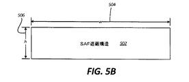
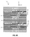
図5Aは、図3Aおよび図3Bの332などのSAFシールドAFM層を排除してdspacingを小さくした(参照番号500で示される)複数センサ読取器の担持面の図である。SAFシールドAFM層を排除できるようにするためには、異なる技術を用いて、SAFシールドAFM層によって与えられるピン止めまたは安定化機能性を達成する/提供する必要がある。1つの実施形態では、SAF遮蔽構造502は、形状(たとえば、SAF502の異なる幅および高さ寸法)によって誘導される一軸異方性によって安定化される。図5Bは、1つの実施形態に従うSAF遮蔽構造502の上面図を示す。図5Bの実施形態では、一軸異方性は、y方向に沿ったSAF遮蔽構造502の(参照番号506で示される)高さhよりも実質的に大きい、x方向に沿ったSAF遮蔽構造502の(参照番号504で示される)幅wを用いることによってSAF遮蔽構造502に与えられる。特定の実施形態では、SAF遮蔽構造502の幅wは、SAF遮蔽構造502の高さhの少なくとも2倍である。形状異方性以外の技術を利用して502などのSAF遮蔽構造における安定化(すなわち自己ピン止め)を与えてもよいことに留意すべきである。当該技術は、好適な整列マグネットよる膜の成長および/または制御された入射角での膜の堆積、好適な熱アニールプロセスなどを含む。
FIG. 5A is a diagram of the bearing surface of a multi-sensor reader (denoted by reference numeral 500) that eliminates the SAF shield AFM layer, such as 332 of FIGS. 3A and 3B, to reduce d spacing . In order to be able to eliminate the SAF shield AFM layer, different techniques must be used to achieve / provide the pinning or stabilization functionality provided by the SAF shield AFM layer. In one embodiment,
図6Aは、dspacingを小さくするために、図3Aおよび図3Bの332などのSAFシールドAFM層が担持面から窪んだ(参照番号600で示される)複数センサ読取器の担持面の図である。図6Bは、(図6Aに示される線A−A′に沿った)センサ積層体の層および担持面に直交する平面を通る、図6Aのマルチセンサ読取器600の断面図である。図6Bで、窪んだSAFシールドAFM層は参照番号602で示される。窪んだSAFシールドAFM層602はdspacingに加わるように寄与しないので、センサ600で得られるdspacingの低減は(図5Aの)センサ500において得られるdspacingの低減と実質的に同様である。センサ600において、SAFシールドAFM602による一方向異方性は、SAFの極性(すなわち、外部ゼロ磁界におけるSAFシールド参照層326およびSAFシールドピンド層330の磁性の向き)が好適に維持されるのを確実にするのを助ける。窪んだSAFシールドAFM層602は、任意の好適な堆積技術を用いて形成されてもよい。異なる実施形態では、SAFシールドAFM層602は、SAFシールドAFM層602がSAFシールド要素315に対する磁気的結合を提供することができる限り、図6Bに示される以外の場所にあってもよいことに留意すべきである。AFMに隣接するSAF磁性層をピンド層(PL)と称し、かつAFMに接していないSAF磁性層を参照層(RL)と称することを一般的に取り決めている。図6Bで、SAFシールドAFM層602は層326の下にありかつ層326に接しているので、層326はPLであり、層330はRLである。SAFシールドAFM層602は、センサのうち1つ(たとえば、センサ302A)のみの中で窪んでいてもよく、他のセンサのSAFシールドAFM層は、図3Bの読取器350中のセンサ302BのSAFシールドAFM層332と同じ場所に位置決めされていてもよいことにも留意すべきである。
FIG. 6A is a view of the support surface of a multi-sensor reader (denoted by reference number 600) with a SAF shield AFM layer, such as 332 in FIGS. 3A and 3B, recessed from the support surface to reduce d spacing . . 6B is a cross-sectional view of the
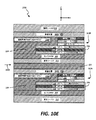
図7Aは、図3Aおよび図3BのSAFシールド参照層326およびSAFシールドスペーサ層328を排除してdspacingを小さくする複数センサ読取器700の担持面の図である。換言すると、(参照番号702で示される)強磁性材料からなる単一の層のみがSAFシールドAFM332によってピン止めされる。層326および328を排除することにより、各々の遮蔽構造314のz方向の厚みが小さくなり得、この結果、センサ全体のdspacingが小さくなり、かつz方向の厚みが小さくなる。ある実施形態では、ピンド層702はNiFeから形成される。他の実施形態では、ピンド層702は、NiFeよりもモーメント値が高い材料から形成されてもよい。相対的に高いモーメントの材料を用いてピンド層702を形成する場合、ピンド層702の厚みは、遮蔽効果の対応する低減なく、NiFeピンド層に対して低減され得る。
FIG. 7A is a diagram of a bearing surface of a
先に示したように、データ記憶媒体あたりのより大きな容量を達成するには、高い線密度を達成することが必須である。パルス幅またはそのピーク振幅の50%での読取パルスの幅であるPW50は潜在的な最大線密度の尺度となる。より広い遷移はより大きなPW50をもたらす。このように、より高い線密度にはより低いPW50が有利である。複数センサ読取器700では、層326、328、および330を含むSAF構造の代わりにピンド層702のみを利用する結果、図7Bに示されるようにPW50が向上し得る。図7Bは、SAF遮蔽構造を有する読取器(たとえば、(図3Aの)読取器300および(図3Bの)350)とピンド層(PL)のみ実施形態とのPW50値の比較を示すグラフである。図7Bで、縦軸704はPW50をnmで表わし、横軸706は厚み(すなわち、ピンド層の厚みおよびSAF構造の厚み)をnmで表わす。プロット708および710(実線)は複数センサ読取器700などのPLのみ実施形態のプロットである。プロット708は、PL702が約1テスラ(T)のモーメント値を有する読取器についてのものであり、プロット710は、PL702が約1.8Tのモーメント値を有する読取器についてのものである。プロット712および714(破線)は、SAF遮蔽構造を有する読取器(たとえば、(図3Aの)読取器300および(図3Bの)350)についてのプロットである。プロット712は、SAFが約1テスラ(T)のモーメント値を有する読取器についてのものであり、プロット714は、SAFが約1.8Tのモーメント値を有する読取器についてのものである。
As indicated above, to achieve greater capacity per data storage medium, it is essential to achieve high linear density. PW50, the width of the read pulse at 50% of the pulse width or its peak amplitude, is a measure of the potential maximum linear density. A wider transition results in a larger PW50. Thus, a lower PW50 is advantageous for higher linear densities. In the
図7Bに見られるように、特定の合計厚みのSAFシールド要素315を含む(図3Aの)300または(図3Bの)350などの読取器の実施形態と比較して、SAFシールド要素315の合計厚みと同じ厚みのPLのみ構造702を有する700などの読取器は、発生するPW50が約3nmだけより小さい。このように、マルチセンサ読取器では、層326、328、および330を含むSAFの代わりにPLのみ構造702を用いることにより、厚みの低減、およびしたがって、dspacingの対応の低減をPW50の劣化なしに得ることができる。たとえば、10nmのPLのみ構造702が生じるPW50は、326などの16nm厚のSAFシールド参照層と330などの16nm厚のSAFシールドピン止め層とを有するSAFシールド要素が生じるPW50と同じである。この例では、SAFシールドをPLのみ構造702と置き換える結果、PW50を劣化させずにdspacingの22nmの縮小が得られる。相対的に高いモーメントの材料を利用して構造702を形成する結果、PW50を劣化させずにdspacingの付加的な縮小(たとえば、約5nmの縮小)を得られる。
As seen in FIG. 7B, the sum of
図7Cは、SAF遮蔽要素315を含む(図3Aの)300または(図3Bの)350などの読取器中のトラック横断磁界伝達曲線714および716を示す。図7Dは、702などのPLのみ構造を含む700などの読取器の実施形態中のトラック横断磁界伝達曲線722および724を示す。図7Cで、縦軸718は、326などのSAFシールド参照層の正規化された磁性(Mx)を表わし、横軸720は、印加される磁界(Hx)をエルステッド(Oe)で表わす。図7Dで、縦軸および横軸は図7Cの軸と同様であるが、図7Dの縦軸は、702などのPLのみ構造の正規化された磁性を表わす。図7Cで、プロット714は、Hxが負の値から正の値に増大するにつれてSAFシールド参照層について得られるMxの値を示す。プロット716は、Hxが正の値から負の値に逆転することから得られるMxの値を示す。プロット722および724はそれぞれプロット714および716と同様であるが、702などのPLのみ構造についてのHxの値の変動に応答したMxの値の変動を示す。図7Cと図7Dとを比較すると、図7C中のゼロMx点726と728との間の距離が図7Dの対応のゼロMx点730と732との間の距離よりも実質的に小さいことが示される。このように、ゼロMx点同士の間の距離の半分である保磁力の幅(または保磁力磁界(H_coercivity))は、図7Cよりも図7Dでより大きい。さらに、Hxがほぼゼロでは、点726と728との間の(参照番号734で示される)平均点は、点730と732との間の(参照番号736で示される)平均点と比較して、左にずれている。このように、平均点でのHxの絶対値(すなわち、ピン止め磁界(H_pinning))は、315などのSAFシールド要素よりも、702などのPLのみ構造についてより低い。PLのみのシールド設計はSAF遮蔽要素と比較してH_pinningがより低いが、H_coercivityがより高く、かつ双方の設計はゼロ磁界で2つの状態を有するので、PLのみの設計は、トラック横断磁界が−700Oeを下回らない限り、SAFシールド設計と同様の安定性を有する。
FIG. 7C shows cross-track magnetic field transfer curves 714 and 716 in a reader such as 300 (of FIG. 3A) or 350 (of FIG. 3B) that includes a
図7Aに示される2センサ読取器700または図7Eに示されるような2つよりも多くのセンサ(302A、302B、および302C)を有する読取器750にPLのみの読取器設計を用いることができる。そのような読取器は、読取器の安定性を保持しながら、PW50、MT10(信号の強度がその最大の10%に低下するデータ記憶媒体上の2つの位置同士の間の距離)/MT50(信号強度がその最大から50%低下するデータ記憶媒体上の2つの位置同士の間の距離)、およびダウントラックdspacingの向上を与えることができる。ヘッドの設計の必要性に依存して、PW50とdspacingとは互いに対して背反となる可能性がある。
A PL-only reader design can be used for the two-
図8Aは、図3Aおよび図3Bの326などのSAFシールド参照層および328などのSAFシールドスペーサ層を排除して、図7A−図7Eに関連して上述した態様でdspacingの縮小が得られる、(参照番号800で示される)複数センサ読取器の担持面の図である。加えて、dspacingのさらなる縮小を得るために、図7Aの332などのSAFシールドAFM層が担持面から窪んでいる。図8Bは、(図8Aに示される線B−B′に沿った)担持面およびセンサ積層体の層に直交する平面を通る、図8Aのマルチセンサ読取器800の断面図である。図8Bで、窪んだSAFシールドAFM層は参照番号802で示される。センサ800において、SAFシールドAFM802による一方向異方性は、PL702の極性(すなわち、外部ゼロ磁界でのPL702の磁化方向)が好適に維持されるのを確実にするのを助ける。窪んだSAFシールドAFM層802は、任意の好適な堆積技術を用いて形成されてもよい。異なる実施形態では、SAFシールドAFM層802は、SAFシールドAFM層802がPL702への磁気的結合を提供することができる限り、図8Bに示されるもの以外の場所にあってもよいことに留意すべきである。SAFシールドAFM層802は、センサのうち1つ(たとえば、センサ302A)のみの中で窪んでいてもよく、他のセンサのSAFシールドAFM層は、図7Aの読取器700中のセンサ302BのSAFシールドAFM層332と同じ場所に位置決めされてもよいことにも留意すべきである。
FIG. 8A eliminates the SAF shield reference layer, such as 326 of FIGS. 3A and 3B, and the SAF shield spacer layer, such as 328, resulting in a reduction in d spacing in the manner described above in connection with FIGS. 7A-7E. , Is a diagram of the bearing surface of a multi-sensor reader (indicated by reference numeral 800). In addition, a SAF shield AFM layer, such as 332 in FIG. 7A, is recessed from the support surface to obtain a further reduction in d spacing . FIG. 8B is a cross-sectional view of the
図9は、図3Aおよび図3Bの326などのSAFシールド参照層および328などのSAFシールドスペーサ層を排除して、たとえば図7Aに関連して上述した態様でdspacingの縮小が得られる、複数センサ読取器900の担持面の図である。加えて、図7Aで用いるAFMシールド層332の代わりに、バイアス硬磁石902が強磁性層904に当接して、強磁性層904の両側から強磁性層904のための必要な安定化を与える。さらに、図9に示される実施形態では、バイアス硬磁石902と軟磁性層906とが側方シールド908の各々で横並びの構成にある。図9のセンサ302Aおよび302Bの各々において、軟磁性層906は、バイアス硬磁石902に静磁的に結合されるかまたは交換結合され、読取られているビットに隣接するビットからの磁束を逸らすように働く。
9 eliminates a SAF shield reference layer, such as 326 in FIGS. 3A and 3B, and a SAF shield spacer layer, such as 328, to obtain a reduction in d spacing , for example, in the manner described above in connection with FIG. 7A. FIG. 6 is a diagram of a carrier surface of a
図10A−図10Eは、図3Bのマルチセンサ読取器350のdspacingに対してdspacingが縮小された、(図10Dおよび図10Eで参照番号1000で示される)マルチセンサ読取器の実施形態をまとめて示す概略図である。図10A−図10Eの実施形態では、x−y平面(すなわち、マルチセンサ読取器の担持面に対して垂直でありかつ読取器の積層体の層に平行な平面)でのSAF遮蔽構造314の形状は、還流磁区を設けるように設計されている。図10A、図10B、および図10Cは、4つの主な磁区(A、B、C、およびD)が形成された例示的な設計の上面図を示す。図10A、図10B、および図10Cに示される頂部は、参照番号1002で示される軟磁性層を含む。永久磁石(PM)またはAFMタブ1004を磁区の1つに結合して、磁区構造のキラル性を制御する。磁区Cは担持面にある。PMタブまたはAFMタブ1004は、磁区A、B、またはDに付けられて、dspacingを増大させることなくキラル性を確実にし得る。PMタブまたはAFMタブ1004は軟磁性層1002の下に位置決めされて担持面から窪んでいてもよいことに留意すべきである。したがって、PMまたはAFMタブ1004は、図10Dのセンサ1000の担持面の図には見えない。しかしながら、PMまたはAFMタブ1004は、(図10Dに示される線C−C′に沿った)担持面およびセンサ積層体の層に直交する平面を通る、図10Dのマルチセンサ読取器1000の断面図である図10Eに示される。PM/AFMタブ1004をBまたはDに付けることの追加の利点は、このタブの向きを(図10Eの参照番号1003で示される)(y方向磁界を有する磁気積層アニールによって設定可能であり、付加的なアニールが必要ないことである。換言すると、PM/AFMタブ1004が磁区BまたはDに付けられる読取器1000の製造の際、センサ積層体302A、302Bおよび安定化特徴(たとえば、PM/AFMタブ1004)の両方のアニールを、担持面に実質的に垂直な軸(たとえばy軸)に沿って1003などの磁界の存在下で単一のアニールステップで行なって、安定化特徴(たとえば、PM/AFMタブ1004)とセンサ積層体AFM SAF層との両方の磁化方向を単一のアニールステップで設定し、これによりセンサ積層体302A、302Bおよび安定化特徴(たとえば、PM/AMFタブ1004)のための別個の磁化方向設定アニールステップを回避し得る。
Figure 10A- FIG. 10E, d spacing is reduced relative to d spacing of the
また別の実施形態では、上述の実施形態の任意のものの中のセンサ302Aとセンサ302Bとの間の絶縁スペーサ層324をアルミナの誘電率値よりも低い誘電率(εr)値(すなわち、約9よりも低いεr値)を有する材料で形成してもよい。厚みが低減された絶縁スペーサ層を形成するのに好適な、εrの値が相対的に低い材料の一例がSiO2であり、これは、約4のεrの値を有する。当然ながら、異なる実施形態では、εrの値が相対的に低い他の誘電材料が好適であってもよい。SiO2のようにεrの値が相対的に低い/小さい場合、たとえば、相対的に厚いアルミナ絶縁スペーサ層のキャパシタンスと比較したキャパシタンスの低下なしに、絶縁スペーサ層324についてより小さな厚みを達成することができる。このように、絶縁スペーサ層324のためにたとえばSiO2を用いる結果、dspacingを縮小し得る。
In yet another embodiment, the insulating
図11A、図11B、および図11Cは、上述の異なるdspacing縮小特徴の組合せを含むマルチ読取器センサ1100の実施形態をまとめて示す。センサ1100において、(遮蔽構造314と同様の)遮蔽構造1102は、(構造315および702と同様の)遮蔽要素1104と、遮蔽要素のための(層またはタブ322、602、802、902、および1004と同様の)安定化機構1106とを一般的に備えて示される。この実施形態では、絶縁スペーサ層324は、SiO2などのεrが相対的に低い材料で形成される。遮蔽要素1104は、NiFeよりも磁気モーメントの値が大きい材料で形成される少なくとも1つの強磁性層を含む。安定化機構1106は、マルチセンサ読取器内の、安定化特徴がdspacingに実質的に付加的に寄与しない位置に位置する遮蔽要素1104とは離れた少なくとも1つの安定化特徴(AFMまたはPMタブ)を含んでもよい(すなわち、少なくとも1つの安定化特徴は、図11B(図11Aの線D−D′に沿った断面図)に示されるように担持面から窪んでいても、または図9に示されるように強磁性層および側方バイアス軟磁性層の側に位置決めされてもよい)。さらに、安定化機構1106の少なくとも一部は、図11Cに示され、かつ図5Aおよび図5Bに関連して上述されたように、形状異方性などのたとえば自己ピン止め技術を用いることによって遮蔽構造1102に組入れられてもよい。先に注記したように、好適であり得る他の自己ピン止め技術は、整列磁石を用いた膜成長および/または制御された入射角での膜の堆積、好適な熱アニールプロセスなどを含む。
11A, 11B, and 11C collectively illustrate an embodiment of a
異なる図は、底部および頂部センサ302Aおよび302Bがz方向に整列されているのを示すが、さまざまな実施形態では、異なるセンサは互いからオフセットされてもよいことに留意すべきである。遮蔽構造の厚みを低減するための技術を単一センサ読取器においても用いて、頂部シールド218と底部シールド222との間の間隔を小さくしてもよいことにも留意すべきである。
It should be noted that although the different views show the bottom and
複数センサ磁気再生装置内のセンサ間の間隔縮小特徴のさまざまな例を出願中に開示するが、実施形態は、出願中に開示される特定の適用例または用例に限定されない。開示のさまざまな実施形態の構造および機能の詳細とともに開示のさまざまな実施形態の数多くの特性および利点を以上の説明で述べたとしても、この開示は例示のみのためのものであり、添付の請求項が表わす用語の広い一般的意味によって示される全範囲までの本開示の原則の範囲内で、特に部品の構造および配置という事項において詳細に変更がなされてもよいことを理解すべきである。たとえば、本開示の範囲および精神から逸脱することなく実質的に同じ機能性を維持しつつセンサ間間隔縮小特徴を有する複数センサ磁気再生装置のための特定の適用例に依存して、特定の要素は異なり得る。さらに、本明細書中に記載の実施形態は、特定のデータ記憶システムで利用される特定の種類の複数センサ磁気再生装置に向けられるが、本開示の範囲および精神から逸脱することなく、本開示の教示を他のデータ記憶装置に適用可能であることが当業者によって認められるであろう。 While various examples of spacing reduction features between sensors in a multi-sensor magnetic regenerator are disclosed in the application, embodiments are not limited to the specific applications or examples disclosed in the application. Although numerous features and advantages of various disclosed embodiments, as well as details of structure and function of various disclosed embodiments, have been set forth in the foregoing description, this disclosure is intended for purposes of illustration only and is subject to the appended claims It should be understood that changes may be made in detail in particular to the structure and arrangement of components within the scope of the principles of the present disclosure to the full extent indicated by the broad general meaning of the terms that the term represents. For example, depending on the particular application for a multi-sensor magnetic regenerator having a reduced sensor spacing feature while maintaining substantially the same functionality without departing from the scope and spirit of the present disclosure, certain elements Can be different. Further, the embodiments described herein are directed to a particular type of multi-sensor magnetic playback device utilized in a particular data storage system, but without departing from the scope and spirit of the present disclosure. It will be appreciated by those skilled in the art that the above teachings can be applied to other data storage devices.
218 頂部シールド、222 底部シールド、300 読取ヘッド、302A,302B センサ、304 センサ反強磁性(AFM)層、305 底部シールド、306 合成反強磁性(SAF)構造、308 スペーサ層、310 フリー層、312 積層キャップ、314 遮蔽構造、315 遮蔽要素、322,906 側方バイアス、324 分離層、350 マルチセンサ読取器、400,500,600,700,750,800,900,1000,1100 センサ読取器、702 ピンド層、802 SAFシールドAFM層、902 硬磁石、1002 軟磁性層、1004 永久磁石またはAFMタブ 218 Top Shield, 222 Bottom Shield, 300 Read Head, 302A, 302B Sensor, 304 Sensor Antiferromagnetic (AFM) Layer, 305 Bottom Shield, 306 Synthetic Antiferromagnetic (SAF) Structure, 308 Spacer Layer, 310 Free Layer, 312 Laminated cap, 314 shielding structure, 315 shielding element, 322,906 lateral bias, 324 separation layer, 350 multi-sensor reader, 400, 500, 600, 700, 750, 800, 900, 1000, 1100 sensor reader, 702 Pinned layer, 802 SAF shield AFM layer, 902 hard magnet, 1002 soft magnetic layer, 1004 permanent magnet or AFM tab
Claims (20)
第1のセンサを備え、前記第1のセンサは、
外部磁界に応じて変化する磁性を有するフリー層(FL)を有するセンサ積層体と、
前記センサ積層体の上に位置決めされる遮蔽構造とを備え、前記遮蔽構造は、遮蔽要素と前記遮蔽要素のための安定化機構とを備え、さらにマルチセンサ読取器は、
前記第1のセンサ上に積層される第2のセンサを備え、前記第2のセンサは、前記外部磁界に応じて変化する磁性を有するFLを有するセンサ積層体を備え、さらにマルチセンサ読取器は、
前記第1のセンサと前記第2のセンサとの間の分離層と、
前記遮蔽構造と前記分離層とのうち少なくとも1つに含まれるFL−FL間隔縮小特徴とを備え、前記FL−FL間隔縮小特徴は、
誘電率値がアルミナよりも低い材料からなる、前記分離層を形成する相対的に薄い層と、
前記遮蔽要素内に組入れられる前記安定化機構と、
前記遮蔽要素とは隔離された、前記マルチセンサ読取器の担持面から窪んだ少なくとも1つの安定化特徴を備える前記安定化機構と、
磁気モーメント値が前記遮蔽要素の少なくとも一部を形成するNiFe以上である材料からなる少なくとも1つの相対的に薄い層と、のうち少なくとも1つを備える、マルチセンサ読取器。 A multi-sensor reader,
A first sensor, the first sensor comprising:
A sensor stack having a free layer (FL) having magnetism that changes in response to an external magnetic field;
A shielding structure positioned on the sensor stack, the shielding structure comprising a shielding element and a stabilization mechanism for the shielding element, and a multi-sensor reader comprising:
A second sensor laminated on the first sensor, the second sensor comprising a sensor laminate having a magnetic FL that changes in response to the external magnetic field, and a multi-sensor reader ,
A separation layer between the first sensor and the second sensor;
FL-FL interval reduction feature included in at least one of the shielding structure and the separation layer, the FL-FL interval reduction feature,
A relatively thin layer forming the separation layer, made of a material having a dielectric constant lower than that of alumina;
The stabilization mechanism incorporated in the shielding element;
The stabilization mechanism comprising at least one stabilization feature recessed from a bearing surface of the multi-sensor reader, isolated from the shielding element;
A multi-sensor reader comprising at least one of at least one relatively thin layer of a material having a magnetic moment value equal to or greater than NiFe forming at least part of the shielding element.
少なくとも1つのセンサを備え、前記少なくとも1つのセンサは、
外部磁界に応じて変化する磁性を有するフリー層を有するセンサ積層体と、
前記センサ積層体の上に位置決めされる遮蔽構造とを備え、前記遮蔽構造は、
磁気モーメント値がNiFe以上である材料からなる少なくとも1つの相対的に薄い層を備える遮蔽要素と、
前記遮蔽要素のための安定化機構とを備える、読取器。 A reader,
Comprising at least one sensor, the at least one sensor comprising:
A sensor stack having a free layer with magnetism that changes in response to an external magnetic field;
A shielding structure positioned on the sensor stack, the shielding structure comprising:
A shielding element comprising at least one relatively thin layer of a material having a magnetic moment value equal to or greater than NiFe;
A reader comprising a stabilization mechanism for the shielding element.
磁気モーメント値がNiFe以上である材料からなる前記少なくとも1つの相対的に薄い層は、合成反強磁性(SAF)構造の相対的に薄いピンド層を備え、前記SAF構造はさらに、磁気モーメント値がNiFe以上である材料から形成される参照層を備える、請求項7に記載の読取器。 The at least one relatively thin layer of material having a magnetic moment value greater than or equal to NiFe comprises a single pinned layer and the shielding element comprises only the single pinned layer, or a magnetic moment value of NiFe The at least one relatively thin layer made of the above material includes a relatively thin pinned layer having a synthetic antiferromagnetic (SAF) structure, and the SAF structure further has a magnetic moment value equal to or greater than NiFe. The reader of claim 7, comprising a reference layer formed from:
外部磁界に応じて変化する磁性を有するフリー層を有するセンサ積層体を形成することと、前記センサ積層体の上に材料の少なくとも1つの相対的に薄い層を備える遮蔽要素を堆積することによって前記センサ積層体の上に遮蔽構造を形成することとによって第1のセンサを形成するステップと、
前記第1のセンサの上に誘電率値がアルミナより低い材料からなる分離層を形成するステップと、
前記分離層の上に第2のセンサを形成するステップとを備える、方法。 A method of forming a multi-sensor reader, comprising:
Forming a sensor stack having a free layer with magnetism that varies in response to an external magnetic field, and depositing a shielding element comprising at least one relatively thin layer of material on the sensor stack. Forming a first sensor by forming a shielding structure on the sensor stack;
Forming a separation layer made of a material having a dielectric constant lower than that of alumina on the first sensor;
Forming a second sensor on the separation layer.
前記センサ積層体の上に材料の前記少なくとも1つの相対的に薄い層を堆積して合成反強磁性(SAF)構造のピンド層を形成することと、
前記ピンド層の上に前記SAF構造の参照層を堆積することとを備える、請求項14に記載の方法。 Depositing the shielding element comprises:
Depositing the at least one relatively thin layer of material on the sensor stack to form a pinned layer of a synthetic antiferromagnetic (SAF) structure;
Depositing a reference layer of the SAF structure on the pinned layer.
前記センサ積層体の第2の側に第2の側方バイアス磁石を形成するステップとをさらに備え、
前記第1の側方バイアス磁石および前記第2の側方バイアス磁石の各々を形成するステップは、少なくとも1つの硬磁性層の一部が前記遮蔽要素の側に位置決めされるように少なくとも1つの硬磁性層を形成して前記遮蔽要素のための前記安定化特徴を設けるステップを備える、請求項14に記載の方法。 Forming a first lateral bias magnet on a first side of the sensor stack;
Forming a second side bias magnet on a second side of the sensor stack,
The step of forming each of the first side bias magnet and the second side bias magnet includes at least one hard magnetic layer such that a portion of at least one hard magnetic layer is positioned on the side of the shielding element. The method of claim 14, comprising forming a magnetic layer to provide the stabilizing feature for the shielding element.
前記還流磁区を設ける複数の磁区のうち選択された1つに前記安定化特徴を装着するステップと、
前記担持面に実質的に垂直な軸に沿った磁界の存在下で単一のアニールステップにおいて前記センサ積層体および前記安定化特徴の両方をアニールして、前記単一のアニールステップにおいて前記安定化特徴とセンサ積層体AFM SAF層との両方の磁化方向を設定し、これにより前記センサ積層体および前記安定化特徴のための別個の磁化方向設定アニールステップを回避するステップとをさらに備える、請求項14に記載の方法。 Shaping the shielding structure to provide a reflux domain in a plane parallel to the layers of the reader stack and perpendicular to the bearing surface of the multi-sensor reader;
Attaching the stabilizing feature to a selected one of a plurality of magnetic domains providing the return magnetic domain;
Annealing both the sensor stack and the stabilizing feature in a single annealing step in the presence of a magnetic field along an axis substantially perpendicular to the bearing surface to stabilize the stabilization in the single annealing step Setting the magnetization direction of both the feature and the sensor stack AFM SAF layer, thereby avoiding a separate magnetizing direction setting annealing step for the sensor stack and the stabilizing feature. 14. The method according to 14.
Applications Claiming Priority (2)
| Application Number | Priority Date | Filing Date | Title |
|---|---|---|---|
| US14/826,798 US9536549B1 (en) | 2015-08-14 | 2015-08-14 | Multiple sensor magnetic reproducing device with reduced inter-sensor spacing |
| US14/826,798 | 2015-08-14 |
Publications (2)
| Publication Number | Publication Date |
|---|---|
| JP2017037699A true JP2017037699A (en) | 2017-02-16 |
| JP2017037699A5 JP2017037699A5 (en) | 2019-05-09 |
Family
ID=57682418
Family Applications (1)
| Application Number | Title | Priority Date | Filing Date |
|---|---|---|---|
| JP2016105076A Pending JP2017037699A (en) | 2015-08-14 | 2016-05-26 | Multi-sensor reader, reader, and method of forming multi-sensor reader |
Country Status (2)
| Country | Link |
|---|---|
| US (1) | US9536549B1 (en) |
| JP (1) | JP2017037699A (en) |
Families Citing this family (10)
| Publication number | Priority date | Publication date | Assignee | Title |
|---|---|---|---|---|
| US9431031B1 (en) | 2015-03-24 | 2016-08-30 | Western Digital (Fremont), Llc | System and method for magnetic transducers having multiple sensors and AFC shields |
| US9870791B1 (en) * | 2016-04-15 | 2018-01-16 | Seagate Technology Llc | Stabilization of one or more upper sensors in multi-sensor readers |
| US9747931B1 (en) | 2016-08-16 | 2017-08-29 | International Business Machines Corporation | Tunnel magnetoresistive sensor having stabilized magnetic shield and dielectric gap sensor |
| US10115418B2 (en) * | 2016-11-21 | 2018-10-30 | Headway Technologies, Inc. | Hard magnet stabilized shield for double (2DMR) or triple (3DMR) dimension magnetic reader structures |
| US10468055B1 (en) | 2017-11-01 | 2019-11-05 | Seagate Technology Llc | Multi-sensor reader having oppositely biased sensing layers |
| US10297279B1 (en) | 2018-04-10 | 2019-05-21 | Seagate Technology Llc | Methods of planarization for device fabrication with head features background |
| US11022511B2 (en) | 2018-04-18 | 2021-06-01 | Aron Kain | Sensor commonality platform using multi-discipline adaptable sensors for customizable applications |
| US10714131B1 (en) * | 2019-02-14 | 2020-07-14 | Headway Technologies, Inc. | Unified dual free layer reader with shared reference layer to enable reduced reader-to-reader separation |
| US11380355B2 (en) | 2020-10-27 | 2022-07-05 | Headway Technologies, Inc. | Adaptive bias control for magnetic recording head |
| US11875828B2 (en) * | 2021-10-14 | 2024-01-16 | Seagate Technology Llc | Magnetic storage reader having a bridge to align magnetic moments |
Citations (6)
| Publication number | Priority date | Publication date | Assignee | Title |
|---|---|---|---|---|
| JPH09147326A (en) * | 1995-09-11 | 1997-06-06 | Internatl Business Mach Corp <Ibm> | Magnetic disk recording apparatus and dual magnetoresistancesensor |
| JP2009289390A (en) * | 2008-05-28 | 2009-12-10 | Tdk Corp | Magnetoresistive device of cpp type, and magnetic disk system |
| JP2014059048A (en) * | 2012-08-21 | 2014-04-03 | Nsk Ltd | Sealing device for bearing and hub unit bearing incorporated with sealing device for bearing |
| JP2015046214A (en) * | 2013-08-28 | 2015-03-12 | シーゲイト テクノロジー エルエルシー | Dual reader structure |
| JP2015049927A (en) * | 2013-08-30 | 2015-03-16 | シーゲイト テクノロジー エルエルシー | Dual reader structure |
| JP2015115088A (en) * | 2013-12-13 | 2015-06-22 | シーゲイト テクノロジー エルエルシー | Magnetoresistive sensor shield |
Family Cites Families (22)
| Publication number | Priority date | Publication date | Assignee | Title |
|---|---|---|---|---|
| JP3234814B2 (en) | 1998-06-30 | 2001-12-04 | 株式会社東芝 | Magnetoresistive element, magnetic head, magnetic head assembly, and magnetic recording device |
| US7656610B1 (en) * | 2006-03-27 | 2010-02-02 | Storage Technology Corporation | Bi-directional magnetic recording head built on a common substrate |
| US8164862B2 (en) | 2008-04-02 | 2012-04-24 | Headway Technologies, Inc. | Seed layer for TMR or CPP-GMR sensor |
| JP5062597B2 (en) * | 2008-08-29 | 2012-10-31 | 独立行政法人産業技術総合研究所 | Tunnel magnetoresistive element |
| US8508880B2 (en) | 2011-02-16 | 2013-08-13 | Seagate Technology Llc | Transducer head with multiple read sensors |
| US20120250189A1 (en) | 2011-03-29 | 2012-10-04 | Tdk Corporation | Magnetic head including side shield layers on both sides of a mr element |
| US8582249B2 (en) * | 2011-04-26 | 2013-11-12 | Seagate Technology Llc | Magnetic element with reduced shield-to-shield spacing |
| US8711517B2 (en) | 2012-04-27 | 2014-04-29 | Seagate Technology Llc | Two dimensional magnetic sensor immune to skew angle misalignment |
| US8786987B2 (en) | 2012-04-27 | 2014-07-22 | Seagate Technology Llc | Biased two dimensional magnetic sensor |
| US20140063644A1 (en) | 2012-08-29 | 2014-03-06 | Seagate Technology Llc | Magnetic Element with Multiple Selective Transducing Elements |
| US8576518B1 (en) | 2012-10-30 | 2013-11-05 | HGST Netherlands B.V. | Current-perpendicular-to-the-plane (CPP) magnetoresistive (MR) sensor with exchange-coupled side shield structure |
| US8638530B1 (en) | 2013-02-20 | 2014-01-28 | HGST Netherlands B.V. | Current-perpendicular-to-the-plane (CPP) magnetoresistive (MR) sensor having a top shield with an antiparallel structure |
| US8824106B1 (en) * | 2013-05-18 | 2014-09-02 | Headway Technologies, Inc. | Two sensor reader for hard disk drive (HDD) |
| US8891207B1 (en) * | 2013-06-07 | 2014-11-18 | Western Digital (Fremont), Llc | Connection schemes for a multiple sensor array usable in two-dimensional magnetic recording |
| US9147431B2 (en) | 2013-08-06 | 2015-09-29 | Seagate Technology Llc | Multi-sensor data transducer |
| US8922935B1 (en) | 2013-08-28 | 2014-12-30 | Seagate Technology Llc | First and second read sensors coupled to a preamplifier via a common signal line |
| US9042058B1 (en) * | 2013-10-17 | 2015-05-26 | Western Digital Technologies, Inc. | Shield designed for middle shields in a multiple sensor array |
| US9087982B2 (en) * | 2013-11-18 | 2015-07-21 | Tdk Corporation | Manufacturing method for pattern multilayer body and mask set |
| US9042059B1 (en) * | 2014-05-15 | 2015-05-26 | HGST Netherlands B.V. | Current-perpendicular-to-the-plane (CPP) magnetoresistive (MR) sensor structure with multiple stacked sensors and improved center shield |
| US8873204B1 (en) * | 2014-07-25 | 2014-10-28 | HGST Netherlands B.V. | Current-perpendicular-to-the-plane (CPP) magnetoresistive (MR) sensor structure with multiple stacked sensors and center shield with CoFeB insertion layer |
| US9099125B1 (en) * | 2014-10-14 | 2015-08-04 | HGST Netherlands B.V. | Current-perpendicular-to-the-plane (CPP) magnetoresistive (MR) sensor structure with stacked sensors for minimization of the effect of head skew |
| US9087527B1 (en) * | 2014-10-28 | 2015-07-21 | Western Digital (Fremont), Llc | Apparatus and method for middle shield connection in magnetic recording transducers |
-
2015
- 2015-08-14 US US14/826,798 patent/US9536549B1/en active Active
-
2016
- 2016-05-26 JP JP2016105076A patent/JP2017037699A/en active Pending
Patent Citations (6)
| Publication number | Priority date | Publication date | Assignee | Title |
|---|---|---|---|---|
| JPH09147326A (en) * | 1995-09-11 | 1997-06-06 | Internatl Business Mach Corp <Ibm> | Magnetic disk recording apparatus and dual magnetoresistancesensor |
| JP2009289390A (en) * | 2008-05-28 | 2009-12-10 | Tdk Corp | Magnetoresistive device of cpp type, and magnetic disk system |
| JP2014059048A (en) * | 2012-08-21 | 2014-04-03 | Nsk Ltd | Sealing device for bearing and hub unit bearing incorporated with sealing device for bearing |
| JP2015046214A (en) * | 2013-08-28 | 2015-03-12 | シーゲイト テクノロジー エルエルシー | Dual reader structure |
| JP2015049927A (en) * | 2013-08-30 | 2015-03-16 | シーゲイト テクノロジー エルエルシー | Dual reader structure |
| JP2015115088A (en) * | 2013-12-13 | 2015-06-22 | シーゲイト テクノロジー エルエルシー | Magnetoresistive sensor shield |
Also Published As
| Publication number | Publication date |
|---|---|
| US9536549B1 (en) | 2017-01-03 |
Similar Documents
| Publication | Publication Date | Title |
|---|---|---|
| US9099125B1 (en) | Current-perpendicular-to-the-plane (CPP) magnetoresistive (MR) sensor structure with stacked sensors for minimization of the effect of head skew | |
| US7599151B2 (en) | Magnetic head with laminated side shields | |
| JP4841112B2 (en) | MTJ sensor and disk drive system | |
| US8873204B1 (en) | Current-perpendicular-to-the-plane (CPP) magnetoresistive (MR) sensor structure with multiple stacked sensors and center shield with CoFeB insertion layer | |
| US9536549B1 (en) | Multiple sensor magnetic reproducing device with reduced inter-sensor spacing | |
| US7035062B1 (en) | Structure to achieve sensitivity and linear density in tunneling GMR heads using orthogonal magnetic alignments | |
| US6667861B2 (en) | Dual/differential GMR head with a single AFM layer | |
| US6947264B2 (en) | Self-pinned in-stack bias structure for magnetoresistive read heads | |
| US9019664B2 (en) | Magnetoresistive sensor with variable shield permeability | |
| US20030235016A1 (en) | Stabilization structures for CPP sensor | |
| US6600184B1 (en) | System and method for improving magnetic tunnel junction sensor magnetoresistance | |
| US6738237B2 (en) | AP-pinned spin valve design using very thin Pt-Mn AFM layer | |
| JP2006157027A (en) | Granular free layer and magnetic head | |
| US9183858B2 (en) | Dual capping layer utilized in a magnetoresistive effect sensor | |
| US9659586B1 (en) | Reader with free layer experiencing opposite phase-shifted media torques | |
| US9685177B2 (en) | Sensor stabilization in a multiple sensor magnetic reproducing device | |
| US9401162B1 (en) | Read sensor with free layers of different widths sandwiching a SAF structure for extremely high resolution | |
| US20040145835A1 (en) | Differential CPP GMR head | |
| US6788502B1 (en) | Co-Fe supermalloy free layer for magnetic tunnel junction heads | |
| US6724586B2 (en) | Bias structure for magnetic tunnel junction magnetoresistive sensor | |
| US9552834B1 (en) | Stabilization of one or more upper sensors in multi-sensor readers | |
| US9870791B1 (en) | Stabilization of one or more upper sensors in multi-sensor readers | |
| US6999285B2 (en) | Spin valve transistor with differential detection and method of making | |
| US9830935B1 (en) | Read sensor capable of providing multiple effective read widths | |
| US9886974B2 (en) | Read head free layer having front and rear portions biased at different levels |
Legal Events
| Date | Code | Title | Description |
|---|---|---|---|
| A521 | Request for written amendment filed |
Free format text: JAPANESE INTERMEDIATE CODE: A523 Effective date: 20190319 |
|
| A621 | Written request for application examination |
Free format text: JAPANESE INTERMEDIATE CODE: A621 Effective date: 20190319 |
|
| A131 | Notification of reasons for refusal |
Free format text: JAPANESE INTERMEDIATE CODE: A131 Effective date: 20190716 |
|
| A601 | Written request for extension of time |
Free format text: JAPANESE INTERMEDIATE CODE: A601 Effective date: 20191015 |
|
| A02 | Decision of refusal |
Free format text: JAPANESE INTERMEDIATE CODE: A02 Effective date: 20200310 |