JP2017011845A - Charger, electric apparatus and charging method - Google Patents
Charger, electric apparatus and charging method Download PDFInfo
- Publication number
- JP2017011845A JP2017011845A JP2015123681A JP2015123681A JP2017011845A JP 2017011845 A JP2017011845 A JP 2017011845A JP 2015123681 A JP2015123681 A JP 2015123681A JP 2015123681 A JP2015123681 A JP 2015123681A JP 2017011845 A JP2017011845 A JP 2017011845A
- Authority
- JP
- Japan
- Prior art keywords
- power storage
- power
- transfer
- unit
- storage unit
- Prior art date
- Legal status (The legal status is an assumption and is not a legal conclusion. Google has not performed a legal analysis and makes no representation as to the accuracy of the status listed.)
- Pending
Links
Images


Classifications
-
- Y—GENERAL TAGGING OF NEW TECHNOLOGICAL DEVELOPMENTS; GENERAL TAGGING OF CROSS-SECTIONAL TECHNOLOGIES SPANNING OVER SEVERAL SECTIONS OF THE IPC; TECHNICAL SUBJECTS COVERED BY FORMER USPC CROSS-REFERENCE ART COLLECTIONS [XRACs] AND DIGESTS
- Y02—TECHNOLOGIES OR APPLICATIONS FOR MITIGATION OR ADAPTATION AGAINST CLIMATE CHANGE
- Y02E—REDUCTION OF GREENHOUSE GAS [GHG] EMISSIONS, RELATED TO ENERGY GENERATION, TRANSMISSION OR DISTRIBUTION
- Y02E60/00—Enabling technologies; Technologies with a potential or indirect contribution to GHG emissions mitigation
- Y02E60/10—Energy storage using batteries
Abstract
Description
この発明は、充電装置、電気機器及び充電方法に関する。 The present invention relates to a charging device, an electric device, and a charging method.
従来、発電手段や外部の電力供給手段から供給された電力を取得して蓄電し、当該蓄電された電力を動作に利用したり、更に外部に電力を供給したりする充電装置や電気機器がある。発電手段としては、太陽光を用いた太陽光発電、太陽熱発電や携帯型機器の振動検知による発電に加え、水力発電や風力発電といった大掛かりなものまで含まれる。また、外部からの電力供給手段としては、電磁誘導を利用した無線充電や、近接場無線通信(Near-Field Communication:NFC)などの通信電波を用いたものがある。 Conventionally, there are charging devices and electrical devices that acquire and store power supplied from power generation means or external power supply means, and use the stored power for operation or supply power to the outside. . The power generation means include not only solar power generation using sunlight, solar thermal power generation, and power generation based on vibration detection of portable devices, but also large-scale devices such as hydroelectric power generation and wind power generation. As an external power supply means, there are those using communication radio waves such as wireless charging using electromagnetic induction and near-field communication (NFC).
電気機器の安定動作、外部への電力の安定供給や容易な管理のため、しばしば、これらの発電手段や電力供給手段が併用されたり、同一のものが複数用いられたりする。特許文献1には、ソーラ発電とNFCの電波による充電とを併用したRFタグにおいて、ソーラ発電により得られた蓄電量が不足した際に、NFCの受信電波から電力を取得することで、内部の蓄電池の残量不足で通信が不可能となる状況を防ぐ技術について開示されている。 For stable operation of electric equipment, stable supply of electric power to the outside, and easy management, these power generation means and power supply means are often used together or a plurality of the same ones are used. In Patent Document 1, in an RF tag that uses both solar power generation and charging by NFC radio waves, when the amount of power stored by solar power generation is insufficient, power is acquired from the received radio waves of NFC, A technique for preventing a situation where communication is impossible due to a shortage of the remaining amount of a storage battery is disclosed.
しかしながら、複数の発電手段や充電手段から同時に電力が供給可能な場合、従来の技術では、供給電圧の最も高い一つの供給元からしか電力を取得することが出来ず、その他の供給元が生かされないので、効率が悪いという課題があった。 However, when power can be supplied simultaneously from a plurality of power generation means and charging means, in the conventional technology, power can be acquired only from one supply source having the highest supply voltage, and other supply sources are not utilized. Therefore, there was a problem that efficiency was bad.
この発明の目的は、より効率良く複数の電力供給手段からの電力を取得して蓄電することの出来る充電装置、電気機器及び充電方法を提供することにある。 An object of the present invention is to provide a charging device, an electric device, and a charging method capable of acquiring and storing power from a plurality of power supply means more efficiently.
上記目的を達成するため、本発明は、
複数の給電元から給電された電力を各々蓄電する複数の第1蓄電手段と、
当該複数の第1蓄電手段に蓄電された電力をまとめて蓄える第2蓄電手段と、
前記複数の第1蓄電手段から前記第2蓄電手段へ各々電力を転送させる転送手段と、
前記転送手段による電力の転送を可能とさせる何れか一つの前記第1蓄電手段を、前記複数の第1蓄電手段の何れか一つの蓄電量に基づいて選択する転送元選択手段と、
を備えることを特徴とする充電装置である。
In order to achieve the above object, the present invention provides:
A plurality of first power storage means for storing power supplied from a plurality of power sources;
Second power storage means for collectively storing the power stored in the plurality of first power storage means;
Transfer means for transferring power respectively from the plurality of first power storage means to the second power storage means;
Transfer source selection means for selecting any one of the first power storage means that enables transfer of power by the transfer means based on any one of the plurality of first power storage means;
It is a charging device characterized by including.
本発明に従うと、より効率良く複数の電力供給手段からの電力を取得して蓄電することが出来るという効果がある。 According to the present invention, there is an effect that power from a plurality of power supply means can be acquired and stored more efficiently.
以下、本発明の実施の形態を図面に基づいて説明する。
[第1実施形態]
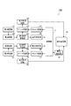
図1は、本発明の充電装置の第1実施形態を示すブロック図である。
充電装置100は、複数の電力の給電元としての第1発電部21及び第2発電部31と、整流回路22、32と、複数の第1蓄電手段としての第1前段蓄電部23及び第2前段蓄電部33と、スイッチ回路24、34と、電力転送回路25、35と、検出手段としての電圧検出部16、26、36と、発振手段としてのチョッパ回路27、37と、転送元選択手段及び転送制御手段としての制御部11と、統合蓄電部12などを備える。
Hereinafter, embodiments of the present invention will be described with reference to the drawings.
[First Embodiment]
FIG. 1 is a block diagram showing a first embodiment of the charging device of the present invention.
The
第1発電部21及び第2発電部31は、それぞれ発電手段として自ら発電動作を行って電力を供給する。第1発電部21及び第2発電部31の発電方法としては、例えば、太陽光発電(太陽電池)、太陽熱発電、風力発電、水力発電や、廃熱などを利用した熱電発電など任意のものが用いられる。第1発電部21の発電方法と第2発電部31の発電方法は、同一であっても異なっていても良い。
The 1st electric
整流回路22、32は、それぞれ、第1発電部21及び第2発電部31から供給される電力を整流する。例えば、整流回路22、32は、第1発電部21や第2発電部31の供給電圧が交流など正負反転する場合に整流すると共に、供給電圧が低下して第1前段蓄電部23や第2前段蓄電部33の電圧よりも低くなった場合における逆流を防止する。
The
第1前段蓄電部23及び第2前段蓄電部33は、それぞれ第1発電部21及び第2発電部31から供給された電力を蓄積する。第1前段蓄電部23及び第2前段蓄電部33の蓄電容量は、統合蓄電部12の蓄電容量よりも十分に小さく、即ち、第1前段蓄電部23及び第2前段蓄電部33の充電時の電圧上昇は、これら第1前段蓄電部23又は第2前段蓄電部33から統合蓄電部12へ電力が転送される場合における統合蓄電部12の電圧上昇よりも早い。また、第1前段蓄電部23及び第2前段蓄電部33の蓄電容量は、第1発電部21及び第2発電部31が供給可能な通常の電力量などを基準として定められれば良い。第1前段蓄電部23の蓄電容量と第2前段蓄電部33の蓄電容量とは、互いに異なっていても良い。
ここでは、第1前段蓄電部23及び第2前段蓄電部33をまとめて前段蓄電部23、33と記す。
The first front-stage
Here, the first pre-stage
スイッチ回路24、34は、第1前段蓄電部23及び第2前段蓄電部33から統合蓄電部12への電力の転送有無をそれぞれ切り替える。スイッチ回路24、34は、制御部11の制御に基づいて電力の転送可否が定められ、電力の転送可能な期間には、制御部11の制御信号に応じて動作するチョッパ回路27、37の出力信号により電力の転送有無が切り替えられる。これらスイッチ回路24、34は、同時に電力の転送を行わないように制御される。スイッチ回路24、34としては、高速な切替動作が可能なアナログスイッチが好ましく用いられる。
The
電力転送回路25、35は、それぞれ、第1前段蓄電部23及び第2前段蓄電部33から統合蓄電部12に電力が転送される際に、当該転送される電力に応じた転送電流が流れる回路である。この電力転送回路25、35は、後述するように、転送電流の損失を抑えつつ短絡電流とならないように電流量を抑える構成を有している。
これらのスイッチ回路24、34及び電力転送回路25、35により転送手段が構成される。
Each of the
These
電圧検出部26、36は、それぞれ、第1前段蓄電部23及び第2前段蓄電部33の出力電圧を検出して制御部11に出力する。電圧検出部26、36は、少なくともこれら出力電圧とスイッチ回路24、34の転送可否に係る基準電圧(蓄電量に係る基準値)とを比較可能であり、例えば、当該基準電圧の検出器や基準電圧との比較器などが用いられる。ここでは、電力の転送を可能とする2種類の基準電圧である高圧側基準電圧VH(動作上限基準値)及び低圧側基準電圧VL(動作下限基準値、選択下限基準値)(高圧側基準電圧VH>低圧側基準電圧VL)が検出される。或いは、これらの電圧検出部26、36は、出力電圧のアナログ値を計測して所定のサンプリング周波数でデジタル変換し、離散多値データとして制御部11に入力させても良い。
The
チョッパ回路27、37は、制御部11から入力される動作制御信号に応じて所定の周波数で発振動作を行い、当該発振動作に応じて生成される駆動信号をスイッチ回路24、34にそれぞれ出力することで、スイッチ回路24、34のオンオフ状態を切り替える。チョッパ回路27、37は、動作制御信号により発振動作を行わない期間には、スイッチ回路24、34をオフ状態(非通電状態)に保つ。
The
制御部11は、電圧検出部26、36から入力された第1前段蓄電部23及び第2前段蓄電部33の出力電圧検出結果に基づいて、スイッチ回路24、34による第1前段蓄電部23及び第2前段蓄電部33から統合蓄電部12への電力転送可否を決定し、電力転送が可能な期間において、チョッパ回路27、37に発振動作を行わせる動作制御信号を出力する。制御部11は、図示略のCPU(Central Processing Unit)、ROM(Read Only Memory)及びRAM(Random Access Memory)などを備えてICチップ上に形成されている。ROMには、スイッチ回路24、34を切替動作させるための制御プログラムが格納されており、CPUは、RAMにより提供される作業用のメモリ空間を用い、この制御プログラムを読み出して実行することでスイッチ回路24、34の切替動作を制御する。制御部11の動作に係る電力は、統合蓄電部12から供給されても良いし、別途外部や図示略の動作用電源部(バッテリ)から供給されても良い。
Based on the output voltage detection results of the first front-stage
統合蓄電部12は、第1前段蓄電部23及び第2前段蓄電部33から転送される電力を蓄積することで、第1発電部21及び第2発電部31により発電された電力を最終的に一括して貯える。統合蓄電部12の蓄電容量は、第1前段蓄電部23及び第2前段蓄電部33の蓄電容量よりも十分大きい。このように蓄電容量の大きいものとして、統合蓄電部12には、例えば、電気二重層コンデンサ(EDLC)や二次電池などが用いられる。統合蓄電部12の蓄電容量は、当該統合蓄電部12に貯えられた電力の使用用途などに応じて適切に定められれば良い。
The integrated
電圧検出部16は、統合蓄電部12の出力電圧を検出して制御部11に出力する。電圧検出部16の構成は、電圧検出部26、36の構成と同様である。制御部11は、第1前段蓄電部23及び第2前段蓄電部33と統合蓄電部12との電圧差に応じて適切な電力転送タイミングや期間を設定することが出来る。
The
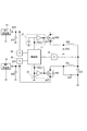
図2は、本実施形態の充電装置100の回路構成を説明する図である。
第1発電部21で発電された電力は、整流回路22のダイオード22Dを介して第1前段蓄電部23のキャパシタ23Cに供給され、蓄電される。ダイオード22Dは、ここでは、キャパシタ23Cから第1発電部21への電流の逆流を防いでいる。
FIG. 2 is a diagram illustrating a circuit configuration of the
The electric power generated by the first
キャパシタ23Cの一端は接地され、他方がダイオード22Dのカソードと接続されている。即ち、当該カソードとの接続側の電圧がキャパシタ23Cの蓄電量に応じて変化する当該キャパシタ23Cの出力電圧となる。キャパシタ23Cの当該出力電圧側は、電圧検出部26及びスイッチ回路24に接続されている。
One end of the
スイッチ回路24は、FET24Tと、当該FET24Tのソース/ドレイン間に接続された還流ダイオード24Dとを備える。FET24Tは、pチャンネル型MOSトランジスタであり、キャパシタ23Cの出力電圧側は、FET24Tのドレイン及び還流ダイオード24Dのカソードに接続される。
The
電圧検出部26による検出結果は、制御部11に入力される。
なお、キャパシタ23Cの蓄電容量などに応じて電圧検出部26とキャパシタ23Cとの間にボルテージフォロワなどを設けて回路を分離しても良い。
A detection result by the
Note that a circuit may be separated by providing a voltage follower or the like between the
チョッパ回路27は、制御部11が出力する動作制御信号と、このチョッパ回路27の出力信号を抵抗素子及びキャパシタにより低域通過させた信号とを比較して、比較結果をスイッチ回路24のFET24Tに出力する。出力信号は、ハイレベルとローレベルの二値であり、ローレベルの出力信号は、制御部11からのローレベル信号より低電圧であり、ハイレベルの出力信号は、制御部11からのハイレベル信号よりも高電圧である。これにより、制御部11からハイレベルの動作制御信号が入力されている間、コンパレータの出力がローレベルからハイレベルに変化した後、抵抗素子の抵抗値とキャパシタの電気容量とにより定まる時定数に応じた時間が経過すると、比較信号が制御部11からのハイレベル信号の電圧以上となってコンパレータの出力がローレベルに切り替わる。また、コンパレータの出力がハイレベルからローレベルに変化した後、上述の時定数に応じた時間が経過すると、比較信号が制御部11からのハイレベル信号の電圧未満となってコンパレータの出力がハイレベルに切り替わる。即ち、チョッパ回路27は発振部を成し、当該発振部の発振動作に応じてスイッチ回路24のFET24Tのオンオフの切り替えが反復して繰り返されることで、スイッチ回路24及び電力転送回路25による電力転送が断続的に行われるチョッピング動作がなされる。
The
なお、制御部11が出力する動作制御信号の電圧値などに応じて、FET24Tがオンされる期間とオフされる期間との比であるデューティ比を変更させることが可能であっても良い。
Note that it may be possible to change the duty ratio, which is the ratio between the period in which the
電力転送回路25は、ダイオード25Dとインダクタ25Lとを備え、FET24Tのソース及び還流ダイオード24Dのアノードは、ダイオード25Dのカソードとインダクタ25Lの一端とに接続されている。インダクタ25Lの他端は、統合蓄電部12のキャパシタ12Cの一端に接続されている。これにより、FET24Tがオンされてソース/ドレイン間に電流が流れる状態では、第1前段蓄電部23から流れる電流が当該インダクタ25Lを通ってキャパシタ12Cに流れ込む。従って、後述するようにFET24Tのオン状態の継続時間がインダクタ25Lのインダクタンスに比して短い場合には、インダクタ25Lにより転送電流の増加が妨げられて第1前段蓄電部23のキャパシタ23Cと統合蓄電部12のキャパシタ12Cとの間の短絡が防止される。
The
ダイオード25Dのアノード側は接地されている。従って、FET24Tのソース/ドレイン間が通電可であるオン期間に、FET24Tのソースから出力される電流は、ダイオード25Dを逆流しない。一方で、FET24Tのソース/ドレイン間が通電不可である期間には、インダクタ25Lに貯えられた磁気エネルギーに応じてダイオード25Dから当該インダクタ25Lを介してキャパシタ12Cへ電流が流れることで、キャパシタ12Cへの充電が継続される。
The anode side of the
キャパシタ12Cのうち、インダクタ25Lに接続された側と反対側は、接地されている。即ち、インダクタ25Lとの接続側の電圧が出力電圧となる。このキャパシタ12Cの出力電圧は、電圧検出部16により検出されて制御部11に入力される。制御部11は、キャパシタ12Cが十分に蓄電されて出力電圧が上昇した場合や、第1発電部21及び第2発電部31の供給電圧が不十分であって電力転送が困難な場合などを判別して、電力転送を中止させることが出来る。
Of the
第2発電部31から統合蓄電部12のキャパシタ12Cまでの回路構成は、上述の第1発電部21からキャパシタ12Cまでの回路構成と同様である。即ち、第2発電部31の供給電圧は、ダイオード32Dを介して第2前段蓄電部33のキャパシタ33Cに貯えられると共に、当該キャパシタ33Cの出力電圧は、電圧検出部36で計測されて制御部11に入力される。制御部11の制御によりチョッパ回路37が動作してスイッチ回路34のFET34Tのゲートにオンオフ信号を入力する。FET34Tのオンオフ状態がインダクタ35Lのインダクタンスに比して短く設定されることで、FET34Tがオン状態では、キャパシタ33Cの出力電圧が電力転送回路35のインダクタ35Lを介して電流を制限されながら統合蓄電部12のキャパシタ12Cに転送される。FET34Tがオフ状態では、インダクタ35Lの磁気エネルギーに応じてダイオード35Dを介して電流が流れ、統合蓄電部12のキャパシタ12Cを充電する。
The circuit configuration from the second
ここで、上述のように、制御部11の制御により、FET24Tのソース/ドレイン間とFET34Tのソース/ドレイン間とが同時に通電可能状態とならないので、第1前段蓄電部23のキャパシタ23Cからの出力電圧と第2前段蓄電部33のキャパシタ33Cからの出力電圧との間に差があっても当該キャパシタ23Cとキャパシタ33Cとの間で電流は流れない。
Here, as described above, the control of the
これらの各構成のうち、電圧検出部16、26、36、制御部11やチョッパ回路27、37など、動作に電力が必要なものについては、適宜統合蓄電部12又は外部電源から電力が供給される。
Among these components, those that require power for operation, such as the
次に、本実施形態の充電装置100における充電制御動作について説明する。
この充電装置100では、複数の発電部である第1発電部21及び第2発電部31の発電が同時に行われている場合に、各々一度第1前段蓄電部23及び第2前段蓄電部33に蓄電し、その後、時分割して各々の電力を統合蓄電部12に転送可能とする。また、電力の転送時には、更に、チョッパ回路27の発振周波数に応じた周期で断続的にFET24T、34Tのオンオフを切り替えるチョッピング動作を行わせる。上述のように、各周期におけるデューティ比が設定可能な場合には、電力の供給元の発電手法や電力転送元と転送先との電圧差などに応じてデューティ比が定められる。
Next, the charging control operation in the
In the
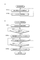
図3は、本実施形態の充電装置100における充電制御処理の制御部11による制御手順を示すフローチャートである。
この充電制御処理は、充電装置100における充電動作が行われる間継続して実行される。
FIG. 3 is a flowchart illustrating a control procedure by the
This charging control process is continuously executed while the charging operation in the
充電制御処理が呼び出されると、制御部11(CPU)は、電力転送元を第1前段蓄電部23に設定する(ステップS101)。それから制御部11は、スイッチング制御処理を呼び出して実行する(ステップS102)。
When the charging control process is called, the control unit 11 (CPU) sets the power transfer source to the first front-stage power storage unit 23 (step S101). Then, the
次いで、制御部11は、電力転送元を第2前段蓄電部33に設定する(ステップS103)。制御部11は、スイッチング制御処理を呼び出して実行する(ステップS104)。それから、制御部11の処理は、ステップS101に戻る。
即ち、本実施形態の充電装置100では、第1前段蓄電部23及び第2前段蓄電部33が交互に(予め設定された順番で)電力転送の対象として選択される。
Next, the
That is, in the
図4は、充電制御処理で呼び出されるスイッチング制御処理の制御部11による制御手順を示すフローチャートである。
FIG. 4 is a flowchart showing a control procedure by the
スイッチング制御処理が呼び出されると、制御部11は、電力転送元の設定を取得する(ステップS201)。制御部11は、電力転送元の出力電圧Vfが高圧側基準電圧VH以上であるか否かを判別する(ステップS202)。高圧側基準電圧VH以上ではないと判別された場合には(ステップS202で“NO”)、制御部11は、ステップS202の処理を繰り返す。或いは、制御部11は、スイッチング制御処理を終了して処理を充電制御処理に戻しても良い。
When the switching control process is called, the
高圧側基準電圧VH以上であると判別された場合には(ステップS202で“YES”)、制御部11は、チョッパ回路27、37に動作制御信号を出力してデューティ比50%で発振動作を開始させる(ステップS203)。これにより、チョッパ回路27又は37から出力される駆動信号に応じてFET24T又はFET34Tが所定の周波数及びデューティ比でチョッピング動作を開始する。
When it is determined that the voltage is equal to or higher than the high-voltage side reference voltage VH (“YES” in step S202), the
制御部11は、電力転送元の出力電圧Vfが低圧側基準電圧VL以上であるか否かを判別する(ステップS204)。低圧側基準電圧VL以上であると判別された場合には(ステップS204で“YES”)、制御部11は、ステップS204の処理を繰り返す。低圧側基準電圧VL以上ではないと判別された場合には(ステップS204で“NO”)、制御部11は、チョッパ回路27、37のうち何れか発振動作中のものによるチョッピング動作を終了させる動作制御信号を出力して、デューティ比を0%とする(ステップS205)。そして、制御部11は、スイッチング制御処理を終了して処理を充電制御処理に戻す。
The
ここで、これら図3、図4で示した制御は、CPUなどを用いずに論理回路などを用いて行うことも出来る。
図5は、充電装置100の変形例の機能構成を示すブロック図である。
この変形例の充電装置100aは、転送元選択手段及び転送制御手段として制御部11の代わりにコントローラ11aが設けられており、その他の構成については上記第1実施形態の充電装置100と同一である。
Here, the control shown in FIGS. 3 and 4 can be performed using a logic circuit or the like without using a CPU or the like.
FIG. 5 is a block diagram illustrating a functional configuration of a modified example of the charging
The
このコントローラ11aは、上述の図3、図4に係る処理を機械的に行う回路を有するLSIなどである。例えば、図3のステップS101、S103の処理は、第1前段蓄電部23と第2前段蓄電部33とを交互に選択するスイッチング素子を備えることでなされる。また、図4におけるステップS202、S204の判別処理の代わりに、それぞれ高圧側基準電圧VH及び低圧側基準電圧VLに係る2つの比較器の出力信号の論理積に応じて発振動作の可否を定めれば良い。この場合、デューティ比は、チョッパ回路27、37の動作により一意に定められる。
The
以上のように、第1実施形態の充電装置100は、複数の発電部(第1発電部21、第2発電部31)から給電された電力を各々蓄電する複数の前段蓄電部23、33(第1前段蓄電部23、第2前段蓄電部33)と、これら前段蓄電部23、33に蓄電された電力をまとめて蓄える統合蓄電部12と、前段蓄電部23、33から統合蓄電部12へ各々電力を転送させるスイッチ回路24、34及び電力転送回路25、35と、この電力の転送を可能とさせる何れか一つの前段蓄電部を、複数の前段蓄電部23、33の何れか一つの蓄電量に基づいて選択する転送元選択手段としての制御部11(或いは、変形例の充電装置100aにおけるコントローラ11a、以下同じ)と、を備える。
このように、複数の前段蓄電部にそれぞれ別個の発電部から充電を行わせつつ、時分割して択一的に前段蓄電部23、33から統合蓄電部12への電力の転送を行うので、複数の発電部のうち、供給電圧が低いものから得られる電力も無駄なく取得することが出来る。従って、より効率良く複数の発電部からの電力を取得して蓄電することが出来る。
As described above, the charging
As described above, since the plurality of previous power storage units are charged from separate power generation units, power is transferred from the previous
また、複数の前段蓄電部23、33の蓄電量を少なくとも予め設定された基準電圧である高圧側基準電圧VH及び低圧側基準電圧VLにより各々検出する電圧検出部26、36を備え、転送制御部としての制御部11は、選択されている前段蓄電部の蓄電量が転送基準値範囲内である下側基準電圧VL以上にあると電圧検出部26、36により検出されている場合に、対応するスイッチ回路及びチョッパ回路によりこの選択されている前段蓄電部の電力を転送させる。従って、前段蓄電部の蓄電量が適切な範囲において効率良く電力の転送を行うことが出来る。
In addition, it includes
また、スイッチ回路24、34がチョッパ回路27、37の動作に応じてチョッピング動作により断続的に電力転送回路25、35を介して電力の転送を行わせるので、一度の電力転送量を抑えつつ細かく合計の転送量を制御することが出来る。
In addition, since the
また、特に、前段蓄電部23、33と統合蓄電部12との間を流れる転送電流の経路となる電力転送回路25、35は、インダクタ25L、35Lを有し、当該インダクタ25L、35Lは、チョッピング動作時において、電力の転送が行われる期間に転送電流を抑えることで前段蓄電部23、33の電圧低下を抑制すると共に、転送が中断された後にダイオード25D、35Dを介して電流を生じさせて統合蓄電部12に蓄電させる。従って、前段蓄電部23、33と統合蓄電部12との間を短絡させず、且つロスなく、電力の転送を行うことが出来る。また、スイッチ回路24、34における通電が中断された期間にも誘導電流を生じさせるので、効率良い電力転送を行わせることが出来る。
Further, in particular, the
また、チョッパ回路27、37を備え、チョッピング動作は、チョッパ回路27、37の発振周波数に応じて行われるので、容易な回路構成で電力転送を断続的に行わせることが出来る。また、発振周波数を適切に維持することが出来るので、インダクタ25L、35Lによる電流抑制と誘導電流の発生を効率良く行わせることが出来る。
Further, since the
また、チョッパ回路27、37は、複数の前段蓄電部23、33に各々対応して設けられ、スイッチ回路24、34は、電力の転送のオンオフを定めるFET24T、34Tを備え、FET24T、34Tは、チョッパ回路27、37が発振周波数に応じて出力する二値信号によりオンオフが切り替えられてチョッピング動作を行う。従って、CPU制御や論理回路などを挟まずに容易な回路構成で直接FET24T、34Tのオンオフの切り替えを行うことが出来る。
The
転送制御手段としての制御部11は、高圧側基準電圧VH以上となったタイミングで選択されている前段蓄電部に対応するチョッパ回路の発振動作を開始させ、低圧側基準電圧VL未満となったタイミングで当該チョッパ回路の発振動作を停止させるので、チョッパ回路の動作に連動してスイッチ回路24、34の動作を容易に制御することが出来、これにより、電力転送回路25、35における電力の転送可否を容易に定めることが出来る。
The
また、転送元選択手段としての制御部11は、予め設定された順番で複数の前段蓄電部23、33のうち一つを選択するので、容易且つバランス良く各発電部21、31からの電力を統合蓄電部12に蓄電させることが出来る。特に、複数の発電部21、31が一定の比で発電可能な場合などには、容易に複数の発電部21、31の供給電力をバランス良く無駄にせずに得ることが出来る。
Further, since the
転送元選択手段としての制御部11は、選択されている前段蓄電部の蓄電量が電圧検出部26、36により低圧側基準電圧VL以下となったことが検出された場合には、前段蓄電部の選択を他に切り替えるので、無駄を省きつつ電力転送可能な前段蓄電部から統合蓄電部12に電力を転送させることが出来る。
The
また、複数の発電部のうち少なくとも2つは、異なる発電手段により電力を発生させることで給電を行うように構成することが出来るので、一方の発電手段が機能し難い環境と、両方の発電手段が同時に発電可能な環境とを問わず、適切に効率良く各発電手段で発電された電力を取得して統合蓄電部12に蓄電させることが出来る。
In addition, since at least two of the plurality of power generation units can be configured to supply power by generating electric power using different power generation means, an environment in which one power generation means is difficult to function and both power generation means Regardless of the environment in which power generation is possible at the same time, the power generated by each power generation means can be acquired appropriately and efficiently and stored in the integrated
また、充電装置において、上述の方法で蓄電を行うことにより、複数の発電部により発電された電力を無駄にせずより効率良く電力を得て統合蓄電部12に蓄電させることが出来る。
Further, in the charging device, by performing power storage by the above-described method, it is possible to efficiently acquire power and store the power in the integrated
[第2実施形態]
次に、第2実施形態の充電装置について説明する。
図6は、本発明の充電装置の第2実施形態の機能構成を示すブロック図である。
この第2実施形態の充電装置100bは、第1実施形態の充電装置100における第2発電部31に代わってアンテナ30a(無線受信部)、RF(Radio Frequency)タグ30及び機能動作部としてのマイコン13(MCU)を備える。また、充電装置100bは、発振手段としてチョッパ回路27、37の代わりに発振部14及び駆動回路28、38を備える。
アンテナ30aは、外部機器50のアンテナ51との無線通信、ここでは、近接場無線通信(Near Field Communication; NFC)が可能なものである。その他の構成は、第1実施形態の充電装置100と同一であり、同一の構成には同一の符号を付して説明を省略する。
[Second Embodiment]
Next, the charging device according to the second embodiment will be described.
FIG. 6 is a block diagram showing a functional configuration of the second embodiment of the charging device of the present invention.
The charging
The
この充電装置100bでは、アンテナ30aにより受信された外部機器50からの送信電波が直接RFタグ30に入力されて信号が復調、解読されると共に、整流回路32により整流された電圧信号により第2前段蓄電部33が充電される。なお、RFタグ30には、統合蓄電部12や外部の動作用電源部などから電力を供給せずに、この第2前段蓄電部33や、図示略の整流回路を介してRFタグ30に入力された電力で直接動作させることとしても良い。
In this
RFタグ30は、NFCによる外部機器50との信号のやりとりに応じた動作を行うICチップである。RFタグ30は、固有識別情報と所定のステータス情報とを記憶する記憶部とを備え、外部機器50からの電波の受信に応じてアンテナ30aから所定の信号が入力されると、外部機器50に対して所定の応答信号を出力する。この応答信号又は応答信号の送信後に更に出力される送信データには、記憶部に記憶された固有識別情報やステータス情報が含まれる。また、外部機器50から新たなステータス情報が入力された場合には、記憶部に記憶されていたステータス情報は、当該新たなステータス情報により上書き更新される。
The
一方、マイコン13は、必要に応じて起動されて統合蓄電部12に蓄電された電力により動作する。マイコン13の動作は、充電装置100bに用途などに応じて適宜設定される。マイコン13とRFタグ30との間は、バスを介して信号の送受信が可能となっており、マイコン13は、RFタグ30のステータス情報などを適宜書き換え更新することが出来る。また、充電装置100bは、マイコン13に加えて種々の用途のCPU、メモリ、記憶部やセンサなどを備えることが出来る。即ち、充電装置100bは、マイコン13を備える電気機器(電子機器を含む)のバッテリとして機能する統合蓄電部12の充電手段を構成する。
On the other hand, the
このように、複数の発電部を有する構成に代えて、1又は複数の発電部と外部から電力の供給を受ける電力受給手段とを備えた充電装置100bにおいて、発電された電力と供給を受けた電力とを並列に蓄電する構成に対しても、上記第1実施形態と同様に時分割を用いた複数の電力転送元からの電力転送及び蓄電が可能である。
Thus, instead of the configuration having a plurality of power generation units, in the
発振部14は、所定の周波数のクロック信号を生成して制御部11に供給する。クロック信号は、制御部11が駆動回路28、38に出力する動作制御信号、即ち、スイッチ回路24、34のオンオフ切替に係るチョッピング動作の制御に用いられる。クロック信号の周波数は、必要に応じて変更可能であっても良いし、固定周波数のクロック信号を生成した後に分周回路を用いて適切な周波数のクロック信号を得ることとしても良い。また、この発振部14は、各駆動回路28、38に対して別個に複数設けられて、異なる位相や周波数の信号を生成しても良い。
The
駆動回路28、38は、制御部11から出力された動作制御信号に応じてスイッチ回路24、34にチョッピング動作を行わせるための駆動信号を出力する。駆動信号は、制御部11から直接スイッチ回路24、34に出力されても良く、この場合には、制御部11が駆動回路28、38として機能する。
The
ここで、本実施形態の充電装置100bでは、電圧検出部26、36、16が電圧値を計測してその計測値のデジタルデータを制御部11に出力することが好ましい。或いは、電圧検出部26、36は、電圧値自体ではなくても統合蓄電部12への電力転送に適した度合いを示す指標となり得る情報を制御部11に出力する。
Here, in the
図7は、第2実施形態の充電装置100bの充電回路に係る回路構成を示す図である。
上述のように、アンテナ30aを介して受信された電波信号は、RFタグ30に入力されると共に、整流回路32のダイオード32Dを介して第2前段蓄電部33のキャパシタ33Cを充電する。
FIG. 7 is a diagram illustrating a circuit configuration according to the charging circuit of the
As described above, the radio wave signal received via the
また、発振部14は、制御部11にクロック信号を出力する。制御部11は、動作制御信号を駆動回路28、38のインバータ28N、38Nに出力して、pMOSトランジスタであるFET24T、34Tのゲート端子に駆動信号を入力させる。
その他の部分については、第1実施形態の充電装置100と同一であり、説明を省略する。
Further, the
About another part, it is the same as the
図8(a)は、本実施形態の充電装置100bで実行される充電制御処理の制御手順を示すフローチャートである。
充電制御処理が開始されると、制御部11は、適切な電力転送元を選択設定する(ステップS101a)。制御部11は、後述のステップS211の処理で既に選択されている場合には、当該選択されている電力転送元に係る情報を取得し、選択されていない場合には、必要に応じて電圧検出部26、36から電圧値の計測値を取得して新たな選択設定を行う。制御部11は、スイッチング制御処理を呼び出して実行する(ステップS102a)。それから、制御部11の処理は、ステップS101aに戻る。
FIG. 8A is a flowchart showing a control procedure of the charging control process executed by the charging
When the charging control process is started, the
図8(b)は、本実施形態の充電装置100bにより実行される充電制御処理で呼び出されるスイッチング制御処理の制御手順を示すフローチャートである。
このスイッチング制御処理は、第1実施形態の充電装置100におけるスイッチング制御処理に対し、ステップS203、S205の処理に代えてステップS203a、S205aの処理が含まれ、また、ステップS211の処理が新たに追加されてその前後で処理の順番が変更された点を除いて同一であり、同一の処理内容には同一の符号を付して説明を省略する。
FIG. 8B is a flowchart showing a control procedure of the switching control process called up in the charging control process executed by the charging
This switching control process includes the processes of steps S203a and S205a instead of the processes of steps S203 and S205 with respect to the switching control process in the
ステップS202の判別処理で“YES”に分岐すると、制御部11は、発振部14に発振動作を開始させると共に、当該発振部14から得られるクロック信号に応じてスイッチ回路24、34にチョッピング動作を行わせる際のデューティ比を50%に設定して、駆動回路28、38へ対応する制御信号を出力する(ステップS203a)。なお、発振部14自体は継続動作させておき、制御部11は、駆動回路28、38への制御信号のみを変更させても良い。制御部11は、第1前段蓄電部23及び第2前段蓄電部33の出力電圧を取得して、所定の条件(選択可能条件)に基づいて現在の電力転送元よりも適切な転送元があるか否かを判別する(ステップS211)。選択可能条件としては、例えば、上述の高圧側基準電圧VHを基準とした所定範囲を設定することが出来る。ないと判別された場合には(ステップS211で“NO”)、制御部11の処理は、ステップS204に移行する。
When branching to “YES” in the determination processing in step S202, the
より適切な転送元があると判別された場合には(ステップS211で“YES”)、制御部11は、発振部14による発振動作を終了させると共に、スイッチ回路24、34のオンオフに係るチョッピング動作のデューティ比を0%とする(ステップS205a)。
When it is determined that there is a more appropriate transfer source (“YES” in step S211), the
ここで、上述のように、電力転送を可能とする電圧範囲を定める高圧側基準電圧VH及び低圧側基準電圧VLは、適宜定められる。これらの値の設定は、各発電部の発電方法や発電能力などに応じて適切に変更させることが出来る。好ましい電圧範囲で電力転送、即ち、第1前段蓄電部23や第2前段蓄電部33からの放電がなされることで、当該放電や充電に係る電力消費をより効率良く抑えることが出来る。このような好ましい電圧範囲は、従来、主に実験的及び又は数値的な取り扱いなどによって知られている。
Here, as described above, the high-voltage side reference voltage VH and the low-voltage side reference voltage VL that define a voltage range in which power transfer is possible are appropriately determined. The setting of these values can be changed appropriately according to the power generation method and power generation capacity of each power generation unit. By transferring power in a preferable voltage range, that is, by discharging from the first pre-stage
図9は、転送範囲設定処理の制御手順を示すフローチャートである。
ここでは、ソーラパネルを用いた太陽光発電と、NFCによる電力受給とを併用した場合を想定した例を示すが、これに限られず、他の発電方法や電力受給方法が用いられる場合には、適宜数値が変更されれば良い。
FIG. 9 is a flowchart showing the control procedure of the transfer range setting process.
Here, an example assuming the case where solar power generation using a solar panel and power reception by NFC are used together is shown, but not limited to this, when other power generation methods and power reception methods are used, The numerical value may be changed as appropriate.
この転送範囲設定処理は、充電装置100bを含む電子機器の出荷前検査や初期設定時に予め実行されて、得られた設定を保持しておくものであっても良いし、充電制御処理とは独立して所定の頻度で実行されても良い。或いは、スイッチング制御処理でステップS201の処理が実行される際に毎回実行されても良い。
This transfer range setting process may be performed in advance during pre-shipment inspection or initial setting of the electronic device including the
転送範囲設定処理が開始されると、制御部11は、発振部14の発振動作を停止して、スイッチ回路24、34の通電に係るデューティ比を「0」に設定する(ステップS301)。制御部11は、対象の電力供給部又は発電部の開放電圧Vopを検出する(ステップS302)。制御部11は、電力供給元がソーラパネル(シリコン型)であるか否かを判別する(ステップS303)。
When the transfer range setting process is started, the
ソーラパネルであると判別された場合には(ステップS303で“YES”)、制御部11は、高圧側基準電圧VHを開放電圧Vopの0.8倍に設定し、また、低圧側基準電圧VLをこの高圧側基準電圧VHの0.9倍に設定した後(ステップS304)。転送範囲設定処理を終了する。
If it is determined that the panel is a solar panel (“YES” in step S303), the
ソーラパネルではないと判別された場合には(ステップS303で“NO”)、制御部11は、高圧側基準電圧VHを開放電圧Vopの0.7倍に設定し、また、低圧側基準電圧VLを開放電圧Vopの0.5倍に設定した後(ステップS305)、転送範囲設定処理を終了する。
If it is determined that the panel is not a solar panel (“NO” in step S303), the
以上のように、第2実施形態の充電装置100bでは、転送制御手段としての制御部11は、転送手段を構成する駆動回路28及びスイッチ回路24によるチョッピング動作のデューティ比を変更可能である。従って、第1発電部21による発電量、アンテナ30aを介して取得される電力量や、前段蓄電部23、33と統合蓄電部12との電圧差などに応じて電力の転送速度を調整したい場合に都合良く設定することが出来る。
As described above, in the
また、高圧側基準電圧VHと低圧側基準電圧VLは、前段蓄電部23、33に対する発電部21、31に応じて各々定められる。これにより、発電手段や電力供給手段に応じて最も効率の良い電圧範囲でそれぞれ電力の転送を行わせることが出来るので、より一層効率良く統合蓄電部12に電力を蓄電させることが出来る。
Further, the high-voltage side reference voltage VH and the low-voltage side reference voltage VL are respectively determined according to the
また、転送元選択手段としての制御部11は、複数の前段蓄電部23、33の出力電圧がそれぞれ高圧側基準電圧VH以上となるか否かを随時又は所定の間隔で監視して、新たに高圧側基準電圧VH以上となった前段蓄電部を選択するので、一の前段蓄電部からの電力の転送中であっても他の前段蓄電部から電力転送をさせると効率が良い場合には、適宜電力を転送させる前段蓄電部を切り替えることが出来るので、更に統合蓄電部12の蓄電を効率良く行わせることが出来る。
In addition, the
また、特に、転送元選択手段としての制御部11は、電圧検出部26、36により、選択されるのに好ましい電圧値以上の前段蓄電部23、33を選択して電力の転送を行わせるので、最適なタイミングで各前段蓄電部23、33から電力の転送を行わせやすい。
In particular, the
また、給電元には、外部からのNFCを用いた送信電波を受信するアンテナ30aが含まれるので、自ら発電する場合だけではなく、外部から供給された電力も適宜混合して統合蓄電部12に蓄電させることが出来る。
In addition, since the power supply source includes an
また、統合蓄電部12に蓄えられた電力を利用して所定の動作を行うマイコン13を備える電気機器としての充電装置100bにより、より効率良く蓄電された電力によってより安定して電気機器としての動作を行うことが可能となる。
In addition, the charging
[第3実施形態]
次に、第3実施形態の充電装置について説明する。
本実施形態の充電装置100cは、4つの発電部を備える。
図10は、第3実施形態の充電装置100cの機能構成を示すブロック図である。
[Third Embodiment]
Next, a charging device according to a third embodiment will be described.
The charging
FIG. 10 is a block diagram illustrating a functional configuration of the
この充電装置100cは、蓄電が3段階に亘って行われる構成となっており、第1発電部21の代わりに第1a発電部21aと第1b発電部21bとを備え、第1実施形態における第2発電部31の代わりに第2a発電部31aと第2b発電部31bとを備える。また、整流回路22a、22b、32a、32bと、第1a前々段蓄電部23aと、第1b前々段蓄電部23bと、第2a前々段蓄電部33aと、第2b前々段蓄電部33bと、スイッチ回路24a、24b、34a、34bと、電力転送回路25a、25b、35a、35bと、電圧検出部26a、26b、36a、36bと、駆動回路28a、28b、38a、38bなどを更に備える。その他の構成については、第2実施形態の充電装置100bと同様であり、同一の構成には同一の符号を付して説明を省略する。
第1a前々段蓄電部23a、第1b前々段蓄電部23b、第2a前々段蓄電部33a及び第2b前々段蓄電部33bが複数の第3蓄電手段をなし、ここでは、まとめて前々段蓄電部23a〜33b等とも記す。
The charging
The 1a pre-stage
第1a発電部21aにより発電された電力は、整流回路22aで整流されて第1a前々段蓄電部23aに蓄電される。第1b発電部21bにより発電された電力は、整流回路22bで整流されて第1b前々段蓄電部23bに蓄電される。第2a発電部31aにより発電された電力は、整流回路32aで整流されて第2a前々段蓄電部33aに蓄電される。第2b発電部31bにより発電された電力は、整流回路32bで整流されて第2b前々段蓄電部33bに蓄電される。
The electric power generated by the 1a
第1a前々段蓄電部23a、第1b前々段蓄電部23b、第2a前々段蓄電部33a、及び第2b前々段蓄電部33bの出力電圧は、それぞれ電圧検出部26a、26b、36a、36bで検出されて検出結果が制御部11に入力される。制御部11は、これらの検出結果に基づいて駆動回路28a、28b、38a、38bに制御信号を出力し、スイッチ回路24a、24b、34a、34bをそれぞれ動作させて、第1a前々段蓄電部23a又は第1b前々段蓄電部23bから第1前段蓄電部23に電力を転送可能とすることが出来、また、第2a前々段蓄電部33a又は第2b前々段蓄電部33bから第2前段蓄電部33に電力を転送可能とすることが出来る。
The output voltages of the first-a pre-stage
第1a発電部21a、第1b発電部21b、第2a発電部31a、及び第2b発電部31bは、それぞれ適宜な発電手段が用いられて良く、これらの発電方法は、同一であっても別個であっても良い。
The 1a
整流回路22a、22b、32a、32bは、それぞれ、適宜な周知の構成を有する。
スイッチ回路24a、24b、34a、34bは、スイッチ回路24、34と同様の構成を有し、電力転送回路25a、25b、35a、35bは、電力転送回路25、35と同様の構成を有する。
同様に、電圧検出部26a、26b、36a、36bは、電圧検出部26、36と同様の構成を有し、駆動回路28a、28b、38a、38bは、駆動回路28、38と同様の構成を有する。
The
The
Similarly, the
第1a前々段蓄電部23a及び第1b前々段蓄電部23bの蓄電容量は、それぞれ、第1前段蓄電部23の蓄電容量よりも十分に小さく、第1a前々段蓄電部23a及び第1b前々段蓄電部23bからそれぞれ一度の電力転送が行われても、第1前段蓄電部23はフルに充電されない。同様に、第2a前々段蓄電部33a及び第2b前々段蓄電部33bの蓄電容量は、それぞれ、第2前段蓄電部33の蓄電容量よりも十分に小さく、第2a前々段蓄電部33a及び第2b前々段蓄電部33bからそれぞれ一度の電力転送が行われても、第2前段蓄電部33はフルに充電されない。
また、第1a前々段蓄電部23aの蓄電容量と第1b前々段蓄電部23bの蓄電容量は、互いに異なっていても良く、第2a前々段蓄電部33aの蓄電容量と第2b前々段蓄電部33bの蓄電容量は、互いに異なっていても良い。
The storage capacities of the 1a pre-stage
In addition, the storage capacity of the 1a pre-stage
次に、第3実施形態の充電装置100cにおける充電制御動作について説明する。
本実施形態の充電装置100cでは、前段蓄電部23、33から統合蓄電部12への電力転送の制御手順は、第1実施形態の充電装置100における制御動作と同一であり、説明を省略する。
Next, the charging control operation in the
In the
第1a前々段蓄電部23a及び第1b前々段蓄電部23bから第1前段蓄電部23への電力転送と、第2a前々段蓄電部33a及び第2b前々段蓄電部33bから第2前段蓄電部33への電力転送とは、独立に行わせることが出来る。電力転送の制御動作は、上記第1実施形態における第1前段蓄電部23及び第2前段蓄電部33から統合蓄電部12への電力転送に係る制御動作と同様に行われるが、第1前段蓄電部23から統合蓄電部12への電力転送が行われている間には、スイッチ回路24a、24bを何れもオフに保たせることとしても良く、また、第2前段蓄電部33から統合蓄電部12への電力転送が行われている間には、スイッチ回路34a、34bを何れもオフに保たせることとしても良い。
Power transfer from the 1a pre-stage
以上のように、第3実施形態の充電装置100cは、複数の前段蓄電部23、33に対してそれぞれ複数ずつ対応付けられて電力を各々蓄電する複数の前々段蓄電部23a〜33bを備え、スイッチ回路24a、24b、34a、34b及び電力転送回路25a、25b、35a、35bにより、複数の前々段蓄電部23a〜33bからこれら前々段蓄電部がそれぞれ対応付けられている前段蓄電部23、33へ各々電力を転送させ、転送元選択手段としての制御部11は、複数の前段蓄電部23、33の各々に電力を転送させる前々段蓄電部23a〜33bを前段蓄電部23、33に対してそれぞれ一つずつ選択する。
このように3段以上の階層状に蓄電部を配置して順次電力を転送させていくことで、電力供給部に接続された各蓄電部からの電力転送の頻度を下げずに効率良く電力を集約することが出来る。また、階層間の蓄電容量の差を極端に大きくしなくて良いので、各蓄電部の蓄電率や蓄電に応じた電圧変化を把握しやすく、電力転送を制御しやすい。
As described above, the charging
By arranging power storage units in three or more layers in this way and sequentially transferring power, power can be efficiently transferred without reducing the frequency of power transfer from each power storage unit connected to the power supply unit. It can be aggregated. Moreover, since the difference in the storage capacity between the tiers does not have to be extremely large, it is easy to grasp the storage rate of each storage unit and the voltage change according to the storage, and it is easy to control the power transfer.
また、転送元選択手段としての制御部11は、異なる前段蓄電部に対して電力を転送させる前々段蓄電部を各々独立に選択する。従って、各蓄電部で入れ替わりで充電と放電とを行わせることで、より効率良く電力の転送を行わせることが出来る。
In addition, the
なお、本発明は、上記実施の形態に限られるものではなく、様々な変更が可能である。
例えば、上記第1実施形態では、統合蓄電部12に転送される電圧の供給元は、第1前段蓄電部23と第2前段蓄電部33の2つとして説明し、第3実施形態では、4つの蓄電部からの電力を2段階に2つずつ統合して最終的に統合蓄電部12集めたが、一度に3つ以上の蓄電部からの電力を統合蓄電部12に集めても良い。
この場合、図11に示したスイッチング制御処理の変形例のように、第1実施形態のスイッチング制御処理におけるステップS202の判別処理で、電力転送元の出力電圧Vfが高圧側基準電圧VH以上ではないと判別された場合には(ステップS202で“NO”)、そのままスイッチング制御処理を終了して当該蓄電部からの電力転送をスキップし、次の順番の蓄電部を選択しても良い。
The present invention is not limited to the above-described embodiment, and various modifications can be made.
For example, in the said 1st Embodiment, the supply source of the voltage transferred to the integrated
In this case, as in the modification example of the switching control process shown in FIG. 11, the output voltage Vf of the power transfer source is not equal to or higher than the high-voltage side reference voltage VH in the determination process in step S202 in the switching control process of the first embodiment. ("NO" in step S202), the switching control process may be terminated as it is, power transfer from the power storage unit may be skipped, and the next power storage unit may be selected.
このように、転送元選択手段としての制御部11は、選択される順番となった前段蓄電部23、33の出力電圧が電圧検出部26、36により低圧側基準電圧VL以上ではないことが検出された場合には、当該選択される順番の前段蓄電部の選択を省略する。従って、夜間の太陽光発電など、発電が暫く見込まれない発電部に係る前段蓄電部への蓄電を待つことなく、現在充電されている前段蓄電部からのみ電力の転送を行わせることが出来るので、より効率良く統合蓄電部12に蓄電させることが出来る。
As described above, the
また、上記実施形態1、2において、順番に複数の前段蓄電部23、33から選択する例と、電力転送をさせるのが好ましい前段蓄電部23、33を随時選択する例を挙げて説明したが、これらに限られない。上記実施の形態を組み合わせて、基本的には順番に選択しつつ、必要に応じて好ましい前段蓄電部からの電力転送を割り込ませても良い。或いは、前段蓄電部23、33からの電力転送が適切に行われる範囲においてランダムに選択されても良い。
In the first and second embodiments, the example in which the plurality of first-stage
また、上記実施の形態では、チョッパ回路27、37又は発振部14の生成する信号を用いてスイッチ回路24、34及び電力転送回路25、35による電力転送時にチョッピング動作を行わせたが、これに限られるものではない。例えば、3段階以上の電力転送が行われる場合で、転送元と転送先の蓄電部の蓄電容量が何れも小さく、転送電流が回路素子にとって問題がない範囲内の場合などでは、チョッピング動作を行わせなくても良い。
Further, in the above embodiment, the chopping operation is performed at the time of power transfer by the
また、チョッピング動作を行わせる場合でも、必ずしもインダクタを用いる必要はない。或いは、インダクタの代わりに大電流を防ぐための構成、例えば、小さな抵抗値を有する抵抗素子を用いても良い。
また、前段蓄電部23、33の選択に係る基準電圧と、前段蓄電部23、33から統合蓄電部12への電力転送可能な電圧範囲とは、別個に設定されても良く、値が異なっていても良い。
Even when a chopping operation is performed, it is not always necessary to use an inductor. Alternatively, a configuration for preventing a large current, for example, a resistance element having a small resistance value may be used instead of the inductor.
In addition, the reference voltage related to the selection of the previous
また、上記実施の形態では、外部からの給電方法としてNFCを用いる例を挙げたが、給電方式は無線に限られず、有線により供給されるものであっても良い。
その他、上記実施の形態で示した具体的な構成や制御手順など細部は、本発明の趣旨を逸脱しない範囲において適宜変更可能である。
In the above embodiment, an example of using NFC as an external power supply method has been described. However, the power supply method is not limited to wireless, and may be supplied by wire.
In addition, details such as the specific configuration and control procedure shown in the above embodiment can be changed as appropriate without departing from the spirit of the present invention.
本発明のいくつかの実施形態を説明したが、本発明の範囲は、上述の実施の形態に限定されるものではなく、特許請求の範囲に記載された発明の範囲とその均等の範囲を含む。
以下に、この出願の願書に最初に添付した特許請求の範囲に記載した発明を付記する。付記に記載した請求項の項番は、この出願の願書に最初に添付した特許請求の範囲の通りである。
Although several embodiments of the present invention have been described, the scope of the present invention is not limited to the above-described embodiments, and includes the scope of the invention described in the claims and equivalents thereof. .
The invention described in the scope of claims attached to the application of this application will be added below. The item numbers of the claims described in the appendix are as set forth in the claims attached to the application of this application.
[付記]
<請求項1>
複数の給電元から給電された電力を各々蓄電する複数の第1蓄電手段と、
当該複数の第1蓄電手段に蓄電された電力をまとめて蓄える第2蓄電手段と、
前記複数の第1蓄電手段から前記第2蓄電手段へ各々電力を転送させる転送手段と、
前記転送手段による電力の転送を可能とさせる何れか一つの前記第1蓄電手段を、前記複数の第1蓄電手段の何れか一つの蓄電量に基づいて選択する転送元選択手段と、
を備えることを特徴とする充電装置。
<請求項2>
前記複数の第1蓄電手段の蓄電量を少なくとも予め設定された基準値で各々検出する検出手段と、
前記選択されている前記第1蓄電手段の蓄電量が所定の転送基準値範囲内にあると前記検出手段により検出されている場合に、前記転送手段により前記選択されている前記第1蓄電手段の電力を転送させる転送制御手段と、
を備えることを特徴とする請求項1記載の充電装置。
<請求項3>
前記転送手段は、断続的に前記転送を行わせるチョッピング動作を行うことを特徴とする請求項1又は2記載の充電装置。
<請求項4>
前記転送手段は、前記第1蓄電手段と前記第2蓄電手段との間を流れる転送電流の経路中にインダクタを有し、当該インダクタは、前記チョッピング動作時において、前記転送が行われる期間に前記転送電流を抑えることで前記第1蓄電手段の電圧低下を抑制すると共に、前記転送が中断された後に電流を生じさせて前記第2蓄電手段に蓄電させることを特徴とする請求項3記載の充電装置。
<請求項5>
前記転送制御手段は、前記転送手段による前記チョッピング動作のデューティ比を変更可能であることを特徴とする請求項3又は4記載の充電装置。
<請求項6>
発振手段を備え、前記チョッピング動作は、前記発振手段の発振周波数に応じて行われることを特徴とする請求項3〜5の何れか一項に記載の充電装置。
<請求項7>
前記発振手段は、前記複数の第1蓄電手段に各々対応して設けられ、
前記転送手段は、前記電力の転送のオンオフを定めるスイッチ回路を備え、
当該スイッチ回路は、前記発振手段が前記発振周波数に応じて出力する二値信号によりオンオフが切り替えられて前記チョッピング動作を行う
ことを特徴とする請求項6記載の充電装置。
<請求項8>
前記複数の第1蓄電手段の蓄電量を少なくとも予め設定された基準値で各々検出する検出手段と、
前記選択されている前記第1蓄電手段の蓄電量が所定の転送基準値範囲内にあると前記検出手段により検出されている場合に、前記転送手段により前記選択されている前記第1蓄電手段の電力を転送させる転送制御手段と、
を備え、
前記転送制御手段は、前記所定の転送基準値範囲の上限である動作上限基準値以上となったタイミングで前記選択されている第1蓄電手段に対応する前記発振手段の発振動作を開始させ、前記所定の転送基準値範囲の下限である動作下限基準値未満となったタイミングで当該発振手段の発振動作を停止させる
ことを特徴とする請求項7記載の充電装置。
<請求項9>
前記所定の転送基準値範囲は、前記第1蓄電手段に対する前記給電元に応じて各々定められることを特徴とする請求項2又は8記載の充電装置。
<請求項10>
前記転送元選択手段は、予め設定された順番で前記複数の第1蓄電手段のうち一つを選択することを特徴とする請求項1〜9の何れか一項に記載の充電装置。
<請求項11>
前記複数の第1蓄電手段の蓄電量を少なくとも予め設定された基準値で各々検出する検出手段を備え、
前記転送元選択手段は、選択される順番となった前記第1蓄電手段の蓄電量が前記検出手段により所定の選択下限基準値以上ではないことが検出された場合には、当該選択される順番の前記第1蓄電手段の選択を省略することを特徴とする請求項10記載の充電装置。
<請求項12>
前記転送元選択手段は、前記複数の第1蓄電手段がそれぞれ所定の選択可能条件を満たすか否かを随時又は所定の間隔で監視して、新たに前記選択可能条件を満たした前記第1蓄電手段を選択することを特徴とする請求項1〜9の何れか一項に記載の充電装置。
<請求項13>
前記複数の第1蓄電手段の蓄電量を少なくとも予め設定された基準値で各々検出する検出手段を備え、
前記転送元選択手段は、前記検出手段により蓄電量が所定の選択可能基準値以上であることが検出されている前記第1蓄電手段を選択することを特徴とする請求項12記載の充電装置。
<請求項14>
前記複数の第1蓄電手段の蓄電量を少なくとも予め設定された基準値で各々検出する検出手段を備え、
前記転送元選択手段は、選択されている前記第1蓄電手段の蓄電量が前記検出手段により所定の選択下限基準値以下となったことが検出された場合には、他の前記第1蓄電手段に選択を切り替えることを特徴とする請求項10〜13の何れか一項に記載の充電装置。
<請求項15>
前記複数の第1蓄電手段に対してそれぞれ複数ずつ対応付けられて電力を各々蓄電する複数の第3蓄電手段を備え、
前記転送手段は、前記複数の第3蓄電手段から当該第3蓄電手段がそれぞれ対応付けられている前記第1蓄電手段へ各々電力を転送させ、
前記転送元選択手段は、前記複数の第1蓄電手段の各々に電力を転送させる前記第3蓄電手段を当該第1蓄電手段に対してそれぞれ一つずつ選択する
ことを特徴とする請求項1〜14の何れか一項に記載の充電装置。
<請求項16>
前記転送元選択手段は、異なる前記1蓄電手段に対して電力を転送させる前記第3蓄電手段を各々独立に選択する
ことを特徴とする請求項15記載の充電装置。
<請求項17>
前記複数の給電元のうち少なくとも2つは、異なる発電手段により電力を発生させることで給電を行うことを特徴とする請求項1〜16の何れか一項に記載の充電装置。
<請求項18>
前記給電元には、外部からの無線充電に係る電磁場変動を取得する無線受信部が含まれることを特徴とする請求項1〜17の何れか一項に記載の充電装置。
<請求項19>
請求項1〜18の何れか一項に記載の充電装置と、
前記第2蓄電手段に蓄えられた電力を利用して所定の動作を行う機能動作部と、
を備えることを特徴とする電気機器。
<請求項20>
複数の第1蓄電手段と、第2蓄電手段とを備える充電装置の充電方法であって、
複数の給電元から給電された電力を複数の第1蓄電手段に各々蓄電させる第1蓄電ステップ、
前記第1蓄電手段から前記第2蓄電手段への電力の転送を可能とさせる何れか一つの前記第1蓄電手段を、前記複数の第1蓄電手段の何れか一つの蓄電量に基づいて選択する転送元選択ステップ
選択された前記第1蓄電手段から第2蓄電手段へ電力を転送させる転送ステップ、
を含むことを特徴とする充電方法。
[Appendix]
<Claim 1>
A plurality of first power storage means for storing power supplied from a plurality of power sources;
Second power storage means for collectively storing the power stored in the plurality of first power storage means;
Transfer means for transferring power respectively from the plurality of first power storage means to the second power storage means;
Transfer source selection means for selecting any one of the first power storage means that enables transfer of power by the transfer means based on any one of the plurality of first power storage means;
A charging device comprising:
<Claim 2>
Detecting means for detecting the amount of electricity stored in the plurality of first power storage means by at least a preset reference value;
When the detection unit detects that the storage amount of the selected first storage unit is within a predetermined transfer reference value range, the first storage unit selected by the transfer unit Transfer control means for transferring power;
The charging device according to claim 1, further comprising:
<Claim 3>
The charging device according to claim 1, wherein the transfer unit performs a chopping operation for intermittently performing the transfer.
<Claim 4>
The transfer means includes an inductor in a path of a transfer current flowing between the first power storage means and the second power storage means, and the inductor is in the period during which the transfer is performed during the chopping operation. 4. The charging according to claim 3, wherein a voltage drop of the first power storage unit is suppressed by suppressing a transfer current, and a current is generated after the transfer is interrupted to store the second power storage unit. apparatus.
<Claim 5>
5. The charging device according to claim 3, wherein the transfer control unit is capable of changing a duty ratio of the chopping operation performed by the transfer unit.
<Claim 6>
6. The charging device according to claim 3, further comprising an oscillating unit, wherein the chopping operation is performed according to an oscillation frequency of the oscillating unit.
<Claim 7>
The oscillation means is provided corresponding to each of the plurality of first power storage means,
The transfer means includes a switch circuit that determines ON / OFF of the transfer of the power,
The charging device according to claim 6, wherein the switch circuit performs the chopping operation by being switched on and off by a binary signal output from the oscillation unit according to the oscillation frequency.
<Claim 8>
Detecting means for detecting the amount of electricity stored in the plurality of first power storage means by at least a preset reference value;
When the detection unit detects that the storage amount of the selected first storage unit is within a predetermined transfer reference value range, the first storage unit selected by the transfer unit Transfer control means for transferring power;
With
The transfer control means starts the oscillation operation of the oscillation means corresponding to the selected first power storage means at a timing when the operation upper limit reference value that is the upper limit of the predetermined transfer reference value range is reached, 8. The charging device according to claim 7, wherein the oscillation operation of the oscillating means is stopped at a timing less than an operation lower limit reference value that is a lower limit of a predetermined transfer reference value range.
<Claim 9>
9. The charging device according to claim 2, wherein the predetermined transfer reference value range is determined according to the power supply source for the first power storage unit.
<Claim 10>
10. The charging device according to claim 1, wherein the transfer source selection unit selects one of the plurality of first power storage units in a preset order.
<Claim 11>
Detecting means for detecting each of the power storage amounts of the plurality of first power storage means with at least a preset reference value;
The transfer source selection unit selects the order of selection when the detection unit detects that the storage amount of the first power storage unit in the order of selection is not greater than or equal to a predetermined selection lower limit reference value. The charging device according to claim 10, wherein selection of the first power storage unit is omitted.
<Claim 12>
The transfer source selection unit monitors whether or not each of the plurality of first power storage units satisfies a predetermined selectable condition at any time or at a predetermined interval, and the first power storage unit newly satisfies the selectable condition. The charging device according to any one of claims 1 to 9, wherein means is selected.
<Claim 13>
Detecting means for detecting each of the power storage amounts of the plurality of first power storage means with at least a preset reference value;
13. The charging device according to
<Claim 14>
Detecting means for detecting each of the power storage amounts of the plurality of first power storage means with at least a preset reference value;
The transfer source selection means, when it is detected by the detection means that the amount of electricity stored in the selected first power storage means is equal to or less than a predetermined selection lower limit reference value, the other first power storage means The charging device according to any one of claims 10 to 13, wherein the selection is switched.
<Claim 15>
A plurality of third power storage means each storing power in association with each of the plurality of first power storage means;
The transfer means causes power to be transferred from the plurality of third power storage means to the first power storage means associated with the third power storage means, respectively.
The transfer source selection unit selects one of the third power storage units that transfer power to each of the plurality of first power storage units, one for each of the first power storage units. The charging device according to any one of 14.
<Claim 16>
The charging device according to claim 15, wherein the transfer source selection unit independently selects the third power storage unit that transfers power to the different one power storage unit.
<Claim 17>
The charging device according to claim 1, wherein at least two of the plurality of power supply sources perform power supply by generating electric power using different power generation means.
<Claim 18>
The charging apparatus according to claim 1, wherein the power supply source includes a wireless reception unit that acquires electromagnetic field fluctuations related to wireless charging from outside.
<Claim 19>
The charging device according to any one of claims 1 to 18,
A functional operation unit that performs a predetermined operation using the electric power stored in the second power storage unit;
An electrical apparatus comprising:
<Claim 20>
A charging method for a charging device comprising a plurality of first power storage means and second power storage means,
A first power storage step of storing power supplied from a plurality of power supply sources in each of a plurality of first power storage means;
One of the first power storage units that enables transfer of electric power from the first power storage unit to the second power storage unit is selected based on one of the plurality of first power storage units. Transfer source selection step Transfer step of transferring power from the selected first power storage means to the second power storage means,
The charging method characterized by including.
11 制御部
11a コントローラ
12 統合蓄電部
12C キャパシタ
13 マイコン
14 発振部
16 電圧検出部
21 第1発電部
21a 第1a発電部
21b 第1b発電部
22、32 整流回路
22D、32D ダイオード
22a、22b、32a、32b 整流回路
23 第1前段蓄電部
23C、33C キャパシタ
23a 第1a前々段蓄電部
23b 第1b前々段蓄電部
24、34 スイッチ回路
24D、34D 還流ダイオード
24a、24b、34a、34b スイッチ回路
25、35 電力転送回路
25D、35D ダイオード
25L、35L インダクタ
25a、25b、35a、35b 電力転送回路
26、36 電圧検出部
26a、26b、36a、36b 電圧検出部
27、37 チョッパ回路
28、38 駆動回路
28N、38N インバータ
28a、28b、38a、38b 駆動回路
30 RFタグ
30a アンテナ
31 第2発電部
31a 第2a発電部
31b 第2b発電部
33 第2前段蓄電部
33a 第2a前々段蓄電部
33b 第2b前々段蓄電部
50 外部機器
51 アンテナ
100 充電装置
100a 充電装置
100b 充電装置
100c 充電装置
DESCRIPTION OF
Claims (20)
当該複数の第1蓄電手段に蓄電された電力をまとめて蓄える第2蓄電手段と、
前記複数の第1蓄電手段から前記第2蓄電手段へ各々電力を転送させる転送手段と、
前記転送手段による電力の転送を可能とさせる何れか一つの前記第1蓄電手段を、前記複数の第1蓄電手段の何れか一つの蓄電量に基づいて選択する転送元選択手段と、
を備えることを特徴とする充電装置。 A plurality of first power storage means for storing power supplied from a plurality of power sources;
Second power storage means for collectively storing the power stored in the plurality of first power storage means;
Transfer means for transferring power respectively from the plurality of first power storage means to the second power storage means;
Transfer source selection means for selecting any one of the first power storage means that enables transfer of power by the transfer means based on any one of the plurality of first power storage means;
A charging device comprising:
前記選択されている前記第1蓄電手段の蓄電量が所定の転送基準値範囲内にあると前記検出手段により検出されている場合に、前記転送手段により前記選択されている前記第1蓄電手段の電力を転送させる転送制御手段と、
を備えることを特徴とする請求項1記載の充電装置。 Detecting means for detecting the amount of electricity stored in the plurality of first power storage means by at least a preset reference value;
When the detection unit detects that the storage amount of the selected first storage unit is within a predetermined transfer reference value range, the first storage unit selected by the transfer unit Transfer control means for transferring power;
The charging device according to claim 1, further comprising:
前記転送手段は、前記電力の転送のオンオフを定めるスイッチ回路を備え、
当該スイッチ回路は、前記発振手段が前記発振周波数に応じて出力する二値信号によりオンオフが切り替えられて前記チョッピング動作を行う
ことを特徴とする請求項6記載の充電装置。 The oscillation means is provided corresponding to each of the plurality of first power storage means,
The transfer means includes a switch circuit that determines ON / OFF of the transfer of the power,
The charging device according to claim 6, wherein the switch circuit performs the chopping operation by being switched on and off by a binary signal output from the oscillation unit according to the oscillation frequency.
前記選択されている前記第1蓄電手段の蓄電量が所定の転送基準値範囲内にあると前記検出手段により検出されている場合に、前記転送手段により前記選択されている前記第1蓄電手段の電力を転送させる転送制御手段と、
を備え、
前記転送制御手段は、前記所定の転送基準値範囲の上限である動作上限基準値以上となったタイミングで前記選択されている第1蓄電手段に対応する前記発振手段の発振動作を開始させ、前記所定の転送基準値範囲の下限である動作下限基準値未満となったタイミングで当該発振手段の発振動作を停止させる
ことを特徴とする請求項7記載の充電装置。 Detecting means for detecting the amount of electricity stored in the plurality of first power storage means by at least a preset reference value;
When the detection unit detects that the storage amount of the selected first storage unit is within a predetermined transfer reference value range, the first storage unit selected by the transfer unit Transfer control means for transferring power;
With
The transfer control means starts the oscillation operation of the oscillation means corresponding to the selected first power storage means at a timing when the operation upper limit reference value that is the upper limit of the predetermined transfer reference value range is reached, 8. The charging device according to claim 7, wherein the oscillation operation of the oscillating means is stopped at a timing less than an operation lower limit reference value that is a lower limit of a predetermined transfer reference value range.
前記転送元選択手段は、選択される順番となった前記第1蓄電手段の蓄電量が前記検出手段により所定の選択下限基準値以上ではないことが検出された場合には、当該選択される順番の前記第1蓄電手段の選択を省略することを特徴とする請求項10記載の充電装置。 Detecting means for detecting each of the power storage amounts of the plurality of first power storage means with at least a preset reference value;
The transfer source selection unit selects the order of selection when the detection unit detects that the storage amount of the first power storage unit in the order of selection is not greater than or equal to a predetermined selection lower limit reference value. The charging device according to claim 10, wherein selection of the first power storage unit is omitted.
前記転送元選択手段は、前記検出手段により蓄電量が所定の選択可能基準値以上であることが検出されている前記第1蓄電手段を選択することを特徴とする請求項12記載の充電装置。 Detecting means for detecting each of the power storage amounts of the plurality of first power storage means with at least a preset reference value;
13. The charging device according to claim 12, wherein the transfer source selection unit selects the first power storage unit that has been detected by the detection unit to have a storage amount equal to or greater than a predetermined selectable reference value.
前記転送元選択手段は、選択されている前記第1蓄電手段の蓄電量が前記検出手段により所定の選択下限基準値以下となったことが検出された場合には、他の前記第1蓄電手段に選択を切り替えることを特徴とする請求項10〜13の何れか一項に記載の充電装置。 Detecting means for detecting each of the power storage amounts of the plurality of first power storage means with at least a preset reference value;
The transfer source selection means, when it is detected by the detection means that the amount of electricity stored in the selected first power storage means is equal to or less than a predetermined selection lower limit reference value, the other first power storage means The charging device according to any one of claims 10 to 13, wherein the selection is switched.
前記転送手段は、前記複数の第3蓄電手段から当該第3蓄電手段がそれぞれ対応付けられている前記第1蓄電手段へ各々電力を転送させ、
前記転送元選択手段は、前記複数の第1蓄電手段の各々に電力を転送させる前記第3蓄電手段を当該第1蓄電手段に対してそれぞれ一つずつ選択する
ことを特徴とする請求項1〜14の何れか一項に記載の充電装置。 A plurality of third power storage means each storing power in association with each of the plurality of first power storage means;
The transfer means causes power to be transferred from the plurality of third power storage means to the first power storage means associated with the third power storage means, respectively.
The transfer source selection unit selects one of the third power storage units that transfer power to each of the plurality of first power storage units, one for each of the first power storage units. The charging device according to any one of 14.
ことを特徴とする請求項15記載の充電装置。 The charging device according to claim 15, wherein the transfer source selection unit independently selects the third power storage unit that transfers power to the different one power storage unit.
前記第2蓄電手段に蓄えられた電力を利用して所定の動作を行う機能動作部と、
を備えることを特徴とする電気機器。 The charging device according to any one of claims 1 to 18,
A functional operation unit that performs a predetermined operation using the electric power stored in the second power storage unit;
An electrical apparatus comprising:
複数の給電元から給電された電力を複数の第1蓄電手段に各々蓄電させる第1蓄電ステップ、
前記第1蓄電手段から前記第2蓄電手段への電力の転送を可能とさせる何れか一つの前記第1蓄電手段を、前記複数の第1蓄電手段の何れか一つの蓄電量に基づいて選択する転送元選択ステップ
選択された前記第1蓄電手段から第2蓄電手段へ電力を転送させる転送ステップ、
を含むことを特徴とする充電方法。 A charging method for a charging device comprising a plurality of first power storage means and second power storage means,
A first power storage step of storing power supplied from a plurality of power supply sources in each of a plurality of first power storage means;
One of the first power storage units that enables transfer of electric power from the first power storage unit to the second power storage unit is selected based on one of the plurality of first power storage units. Transfer source selection step Transfer step of transferring power from the selected first power storage means to the second power storage means,
The charging method characterized by including.
Priority Applications (1)
| Application Number | Priority Date | Filing Date | Title |
|---|---|---|---|
| JP2015123681A JP2017011845A (en) | 2015-06-19 | 2015-06-19 | Charger, electric apparatus and charging method |
Applications Claiming Priority (1)
| Application Number | Priority Date | Filing Date | Title |
|---|---|---|---|
| JP2015123681A JP2017011845A (en) | 2015-06-19 | 2015-06-19 | Charger, electric apparatus and charging method |
Publications (1)
| Publication Number | Publication Date |
|---|---|
| JP2017011845A true JP2017011845A (en) | 2017-01-12 |
Family
ID=57761961
Family Applications (1)
| Application Number | Title | Priority Date | Filing Date |
|---|---|---|---|
| JP2015123681A Pending JP2017011845A (en) | 2015-06-19 | 2015-06-19 | Charger, electric apparatus and charging method |
Country Status (1)
| Country | Link |
|---|---|
| JP (1) | JP2017011845A (en) |
Citations (12)
| Publication number | Priority date | Publication date | Assignee | Title |
|---|---|---|---|---|
| JP2005160290A (en) * | 2003-10-30 | 2005-06-16 | Sharp Corp | Independent source system |
| WO2007086472A1 (en) * | 2006-01-27 | 2007-08-02 | Sharp Kabushiki Kaisha | Power supply system |
| JP2008182810A (en) * | 2007-01-24 | 2008-08-07 | Matsushita Electric Ind Co Ltd | Electronic equipment system and battery pack |
| JP2010142044A (en) * | 2008-12-12 | 2010-06-24 | Nec Tokin Corp | Weak power converter |
| JP2010165314A (en) * | 2009-01-19 | 2010-07-29 | Panasonic Electric Works Co Ltd | Entrance/exit management system |
| JP2010272219A (en) * | 2009-05-19 | 2010-12-02 | Ntt Facilities Inc | Charge control device for lithium ion battery pack, and lithium ion battery pack system |
| JP2010288393A (en) * | 2009-06-12 | 2010-12-24 | Sharp Corp | Power operation system, power operation method, photovoltaic power generator, and controller |
| JP2012019675A (en) * | 2010-07-11 | 2012-01-26 | Triune Ip Llc | Dynamic energy harvesting control |
| JP2012244846A (en) * | 2011-05-23 | 2012-12-10 | Mitsubishi Electric Engineering Co Ltd | Environmental power generation apparatus, environmental power generation system and sensor device |
| JP2013201795A (en) * | 2012-03-23 | 2013-10-03 | Sharp Corp | Photovoltaic power generation system with power storage device |
| JP2014016729A (en) * | 2012-07-06 | 2014-01-30 | Rohm Co Ltd | Power management circuit, electronic apparatus, and radio sensor |
| JP2014239559A (en) * | 2011-09-28 | 2014-12-18 | 三洋電機株式会社 | Power storage system |
-
2015
- 2015-06-19 JP JP2015123681A patent/JP2017011845A/en active Pending
Patent Citations (12)
| Publication number | Priority date | Publication date | Assignee | Title |
|---|---|---|---|---|
| JP2005160290A (en) * | 2003-10-30 | 2005-06-16 | Sharp Corp | Independent source system |
| WO2007086472A1 (en) * | 2006-01-27 | 2007-08-02 | Sharp Kabushiki Kaisha | Power supply system |
| JP2008182810A (en) * | 2007-01-24 | 2008-08-07 | Matsushita Electric Ind Co Ltd | Electronic equipment system and battery pack |
| JP2010142044A (en) * | 2008-12-12 | 2010-06-24 | Nec Tokin Corp | Weak power converter |
| JP2010165314A (en) * | 2009-01-19 | 2010-07-29 | Panasonic Electric Works Co Ltd | Entrance/exit management system |
| JP2010272219A (en) * | 2009-05-19 | 2010-12-02 | Ntt Facilities Inc | Charge control device for lithium ion battery pack, and lithium ion battery pack system |
| JP2010288393A (en) * | 2009-06-12 | 2010-12-24 | Sharp Corp | Power operation system, power operation method, photovoltaic power generator, and controller |
| JP2012019675A (en) * | 2010-07-11 | 2012-01-26 | Triune Ip Llc | Dynamic energy harvesting control |
| JP2012244846A (en) * | 2011-05-23 | 2012-12-10 | Mitsubishi Electric Engineering Co Ltd | Environmental power generation apparatus, environmental power generation system and sensor device |
| JP2014239559A (en) * | 2011-09-28 | 2014-12-18 | 三洋電機株式会社 | Power storage system |
| JP2013201795A (en) * | 2012-03-23 | 2013-10-03 | Sharp Corp | Photovoltaic power generation system with power storage device |
| JP2014016729A (en) * | 2012-07-06 | 2014-01-30 | Rohm Co Ltd | Power management circuit, electronic apparatus, and radio sensor |
Similar Documents
| Publication | Publication Date | Title |
|---|---|---|
| US8786247B2 (en) | Charging circuit | |
| US10389274B2 (en) | Boosted output inverter for electronic devices | |
| US9998003B2 (en) | DC-DC converter, power receiving device, and power feeding system | |
| CN101640476A (en) | Power regulator and control method thereof | |
| TW202118214A (en) | Quasi-resonant valley lockout without feedback reference | |
| CN113342154A (en) | Multiple power management integrated circuits and devices with dual pin interface | |
| US20170179831A1 (en) | Zero voltage switching flyback converter | |
| CN104795997A (en) | Forward converter and secondary side switch controller | |
| US7796405B2 (en) | Phase shifted DC-DC converter with improved efficiency at light load | |
| US8471404B2 (en) | System and method for supporting high burst current in a current limited system | |
| TW201822423A (en) | Energy harvest system and control method thereof | |
| US10587126B2 (en) | Power storage device, power storage control device, and power storage control method | |
| CN104578780B (en) | DC-DC converter | |
| US8723485B2 (en) | Power supply system | |
| Syed et al. | RF energy harvesting chip powered sensor node | |
| US9407099B2 (en) | Two-way direct balance circuit for series cells | |
| JP5398629B2 (en) | Charge / discharge inspection equipment | |
| US11108327B2 (en) | Selected-parameter adaptive switching for power converters | |
| Lee et al. | A rectifier-reusing bias-flip energy harvesting interface circuit with adaptively reconfigurable SC converter for wind-driven triboelectric nanogenerator | |
| JP6565339B2 (en) | Charging device, electronic device, and charging method | |
| JP2015171280A (en) | Voltage equalization device and power storage device | |
| JP2017011845A (en) | Charger, electric apparatus and charging method | |
| CN207926553U (en) | A kind of multifunction switch controller | |
| JP6268357B1 (en) | Power storage device and control method thereof | |
| KR101483517B1 (en) | Apparatus for controlling charging and discharging of batterry in step down converter for dc power grid |
Legal Events
| Date | Code | Title | Description |
|---|---|---|---|
| A621 | Written request for application examination |
Free format text: JAPANESE INTERMEDIATE CODE: A621 Effective date: 20180523 |
|
| A977 | Report on retrieval |
Free format text: JAPANESE INTERMEDIATE CODE: A971007 Effective date: 20190222 |
|
| A131 | Notification of reasons for refusal |
Free format text: JAPANESE INTERMEDIATE CODE: A131 Effective date: 20190319 |
|
| A521 | Request for written amendment filed |
Free format text: JAPANESE INTERMEDIATE CODE: A523 Effective date: 20190403 |
|
| A131 | Notification of reasons for refusal |
Free format text: JAPANESE INTERMEDIATE CODE: A131 Effective date: 20191001 |
|
| A521 | Request for written amendment filed |
Free format text: JAPANESE INTERMEDIATE CODE: A523 Effective date: 20191121 |
|
| A131 | Notification of reasons for refusal |
Free format text: JAPANESE INTERMEDIATE CODE: A131 Effective date: 20200428 |
|
| A02 | Decision of refusal |
Free format text: JAPANESE INTERMEDIATE CODE: A02 Effective date: 20201027 |