JP2017005656A - Phase abnormality detection device and array antenna system - Google Patents

Phase abnormality detection device and array antenna system Download PDF

Info

Publication number
JP2017005656A
JP2017005656A JP2015121056A JP2015121056A JP2017005656A JP 2017005656 A JP2017005656 A JP 2017005656A JP 2015121056 A JP2015121056 A JP 2015121056A JP 2015121056 A JP2015121056 A JP 2015121056A JP 2017005656 A JP2017005656 A JP 2017005656A
Authority
JP
Japan
Prior art keywords
signal
phase
unit
antenna element
extraction unit
Prior art date
Legal status (The legal status is an assumption and is not a legal conclusion. Google has not performed a legal analysis and makes no representation as to the accuracy of the status listed.)
Pending
Application number
JP2015121056A
Other languages
Japanese (ja)
Inventor
前畠 貴
Takashi Maehata
貴 前畠
Current Assignee (The listed assignees may be inaccurate. Google has not performed a legal analysis and makes no representation or warranty as to the accuracy of the list.)
Sumitomo Electric Industries Ltd
Original Assignee
Sumitomo Electric Industries Ltd
Priority date (The priority date is an assumption and is not a legal conclusion. Google has not performed a legal analysis and makes no representation as to the accuracy of the date listed.)
Filing date
Publication date
Application filed by Sumitomo Electric Industries Ltd filed Critical Sumitomo Electric Industries Ltd
Priority to JP2015121056A priority Critical patent/JP2017005656A/en
Publication of JP2017005656A publication Critical patent/JP2017005656A/en
Pending legal-status Critical Current

Links

Images

Abstract

PROBLEM TO BE SOLVED: To provide a phase abnormality detection device and an array antenna system capable of detecting phase abnormalities of a signal transmitted from an antenna element in communication.SOLUTION: A phase abnormality detection device that detects phase abnormalities at the time when a signal whose phase is adjusted by a phase shifter is transmitted from an antenna element, comprises: a reflection signal extraction unit that extracts a reflection signal from the antenna element in a path from the phase shifter to the antenna element; and a determination unit that determines presence or absence of the phase abnormalities on the basis of the reflection signal extracted by the reflection signal extraction unit.SELECTED DRAWING: Figure 3

Description

本発明は、無線通信システムの基地局装置等に用いられる位相異常検出装置及びアレーアンテナシステムに関する。   The present invention relates to a phase abnormality detection device and an array antenna system used in a base station device or the like of a wireless communication system.

近年、携帯電話等に用いられる無線通信システムにおいては、スマートフォン等の普及により、通信エリアの拡大や通信容量の拡張に対する要求が高まっている。そこで、高周波送受信機の機能を内蔵したアクティブアンテナシステムの基地局装置への利用が検討されている。
アクティブアンテナシステムは、複数のアンテナ素子と、複数のアンテナ素子それぞれに対応して設けられた複数の送受信部とを備えている。このため、アンテナ素子ごとに送受信される無線信号を制御することができ制御性に優れており、この優れた制御性を利用して通信環境を向上し得る新たなサービスの提供が可能となる(例えば、特許文献1参照)。
In recent years, in wireless communication systems used for mobile phones and the like, demands for expansion of communication areas and expansion of communication capacity are increasing due to the spread of smartphones and the like. Then, utilization of the active antenna system incorporating the function of a high frequency transmitter / receiver to the base station apparatus is examined.
The active antenna system includes a plurality of antenna elements and a plurality of transmission / reception units provided corresponding to the plurality of antenna elements. For this reason, the radio signal transmitted / received for each antenna element can be controlled, and the controllability is excellent, and it is possible to provide a new service that can improve the communication environment by using this excellent controllability ( For example, see Patent Document 1).

特表2009−544205号公報Special table 2009-544205 gazette

上記アクティブアンテナシステムでは、各アンテナ素子から送信される無線周波数信号(RF信号)が所望の方向に送信されるように、工場出荷時に各無線周波数信号の位相が適正な値となるように予め設定されている。
しかし、工場から出荷されて設置現場にアンテナ素子が設置されるまでの間に、例えば運搬中のアンテナ素子が他部材と干渉して変形することが想定される。このような場合には、設置場所において実際に通信するときに、変形したアンテナ素子から送信される無線周波数信号の位相が変化することで、所望の方向に無線周波数信号を送信することができなくなるおそれがある。
In the above active antenna system, the phase of each radio frequency signal is set in advance at the factory so that the radio frequency signal (RF signal) transmitted from each antenna element is transmitted in a desired direction. Has been.
However, it is assumed that, for example, the antenna element being transported interferes with other members and is deformed before the antenna element is installed at the installation site after being shipped from the factory. In such a case, when actually communicating at the installation location, the phase of the radio frequency signal transmitted from the deformed antenna element changes, so that the radio frequency signal cannot be transmitted in a desired direction. There is a fear.

本発明はこのような事情に鑑みてなされたものであり、通信中においてアンテナ素子から送信される信号の位相異常を検出することができる位相異常検出装置及びアレーアンテナシステムを提供することを目的とする。   The present invention has been made in view of such circumstances, and an object thereof is to provide a phase abnormality detection device and an array antenna system capable of detecting a phase abnormality of a signal transmitted from an antenna element during communication. To do.

本発明の一態様に係る位相異常検出装置は、移相器により位相が調整された信号をアンテナ素子から送信するときの位相異常を検出する位相異常検出装置であって、前記移相器から前記アンテナ素子に至る経路において当該アンテナ素子からの反射信号を取り出す反射信号取出部と、前記反射信号取出部により取り出された前記反射信号に基づいて前記位相異常の有無を判定する判定部と、を備える位相異常検出装置である。   A phase abnormality detection apparatus according to an aspect of the present invention is a phase abnormality detection apparatus that detects a phase abnormality when a signal whose phase is adjusted by a phase shifter is transmitted from an antenna element. A reflection signal extraction unit that extracts a reflection signal from the antenna element in a path to the antenna element; and a determination unit that determines the presence or absence of the phase abnormality based on the reflection signal extracted by the reflection signal extraction unit. It is a phase abnormality detection device.

本発明の一態様に係るアレーアンテナシステムは、複数のアンテナ素子と、これらの各アンテナ素子から送信される信号の位相を個別に調整する複数の移相器と、前記各移相器から対応する前記アンテナ素子に至る経路において当該アンテナ素子からの反射信号を取り出す複数の反射信号取出部と、前記各反射信号取出部により取り出された前記反射信号に基づいて、対応する前記アンテナ素子から送信される信号の位相異常の有無を判定する判定部と、を備えるアレーアンテナシステムである。   An array antenna system according to an aspect of the present invention corresponds to a plurality of antenna elements, a plurality of phase shifters that individually adjust the phases of signals transmitted from the antenna elements, and the phase shifters. A plurality of reflected signal extraction units that extract reflected signals from the antenna element in a path to the antenna element, and the reflected signals extracted by the reflected signal extraction units are transmitted from the corresponding antenna elements. An array antenna system comprising: a determination unit that determines presence / absence of a signal phase abnormality.

本発明によれば、通信中においてアンテナ素子から送信される信号の位相異常を検出することができる。   ADVANTAGE OF THE INVENTION According to this invention, the phase abnormality of the signal transmitted from an antenna element can be detected during communication.

本発明の一実施形態に係るアレーアンテナシステムを備えた基地局装置の一部を示すブロック図である。It is a block diagram which shows a part of base station apparatus provided with the array antenna system which concerns on one Embodiment of this invention. アンテナシステムの送信側の構成を示すブロック図である。It is a block diagram which shows the structure of the transmission side of an antenna system. アンテナシステムの制御構成を示すブロック図である。It is a block diagram which shows the control structure of an antenna system. 制御部が出力信号の経路調整の確認工程を実行するときのブロック図である。It is a block diagram when a control part performs the confirmation process of the path | route adjustment of an output signal. 位相とこれに対応する利得及び通過ロスとの関係を示すルックアップテーブルの一例である。It is an example of the look-up table which shows the relationship between a phase, the gain corresponding to this, and a passage loss. 制御部が移相器の制御工程を実行するときのブロック図である。It is a block diagram when a control part performs the control process of a phase shifter. (A)は移相器を制御する前の初期状態における合成信号の電圧波形、(B)は移相器の制御電圧を変化させたときの合成信号の電圧波形、(C)及び(D)は移相器の制御電圧を変化させたときの合成信号の他の電圧波形である。(A) is the voltage waveform of the synthesized signal in the initial state before controlling the phase shifter, (B) is the voltage waveform of the synthesized signal when the control voltage of the phase shifter is changed, (C) and (D). Is another voltage waveform of the synthesized signal when the control voltage of the phase shifter is changed. 制御部が反射信号の状態確認工程を実行するときのブロック図である。It is a block diagram when a control part performs the state confirmation process of a reflected signal.

[本発明の実施形態の説明]
最初に本発明の実施形態の内容を列記して説明する。
(1)本発明の実施形態に係る位相異常検出装置は、移相器により位相が調整された信号をアンテナ素子から送信するときの位相異常を検出する位相異常検出装置であって、前記移相器から前記アンテナ素子に至る経路において当該アンテナ素子からの反射信号を取り出す反射信号取出部と、前記反射信号取出部により取り出された前記反射信号に基づいて前記位相異常の有無を判定する判定部と、を備える。
[Description of Embodiment of the Present Invention]
First, the contents of the embodiment of the present invention will be listed and described.
(1) A phase abnormality detection device according to an embodiment of the present invention is a phase abnormality detection device that detects a phase abnormality when a signal whose phase is adjusted by a phase shifter is transmitted from an antenna element. A reflection signal extraction unit that extracts a reflection signal from the antenna element in a path from the device to the antenna element; and a determination unit that determines presence or absence of the phase abnormality based on the reflection signal extracted by the reflection signal extraction unit; .

上記位相異常検出装置によれば、反射信号取出部により取り出されたアンテナ素子からの反射信号に基づいて位相異常の有無を判定する判定部を備えているので、アンテナ素子から送信される信号に位相異常が生じたときに、そのアンテナ素子の反射信号に変化が生じれば、当該アンテナ素子から送信される信号に位相異常が有ると判定し、その異常を検出することができる。このため、通信中であってもアンテナ素子から送信される信号の位相異常を検出することができる。   According to the phase abnormality detection device, since the determination unit that determines the presence / absence of phase abnormality based on the reflected signal from the antenna element extracted by the reflected signal extraction unit is provided, the phase transmitted to the signal transmitted from the antenna element If a change occurs in the reflected signal of the antenna element when an abnormality occurs, it can be determined that the signal transmitted from the antenna element has a phase abnormality, and the abnormality can be detected. For this reason, even during communication, it is possible to detect the phase abnormality of the signal transmitted from the antenna element.

(2)前記位相異常検出装置において、前記反射信号取出部が過去に取り出した前記反射信号に基づく情報を記憶するための記憶部をさらに備え、前記判定部は、過去の前記反射信号に基づく情報と、現在の前記反射信号に基づく情報とに基づいて、前記位相異常の有無を判定するのが好ましい。
この場合、例えば、工場出荷時に前記反射信号取出部が取り出した反射信号に基づく情報と、現時点で前記反射信号取出部が取り出した反射信号に基づく情報とを比較することで、判定部は経時的な判定を行うことができ、位相異常の有無をより精度良く検出することができる。
(2) In the phase abnormality detection device, the reflection signal extraction unit further includes a storage unit for storing information based on the reflection signal extracted in the past, and the determination unit includes information based on the past reflection signal. It is preferable to determine the presence or absence of the phase abnormality based on the current information based on the reflected signal.
In this case, for example, by comparing the information based on the reflection signal extracted by the reflection signal extraction unit at the time of shipment from the factory with the information based on the reflection signal extracted by the reflection signal extraction unit at the present time, the determination unit Determination can be made, and the presence or absence of phase abnormality can be detected with higher accuracy.

(3)前記位相異常検出装置において、前記判定部は、前記位相異常が有ると判定した場合、その判定結果を報知する指令を出力するのが好ましい。
この場合、判定部が位相異常が有ることを報知する指令を出力することで、アンテナ素子から送信される信号に位相異常が生じたことを容易に把握することができる。
(3) In the phase abnormality detection device, when the determination unit determines that the phase abnormality is present, it preferably outputs a command for informing the determination result.
In this case, it is possible to easily grasp that the phase abnormality has occurred in the signal transmitted from the antenna element by outputting a command for notifying that the determination unit has the phase abnormality.

(4)本発明の実施形態に係るアレーアンテナシステムは、複数のアンテナ素子と、これらの各アンテナ素子から送信される信号の位相を個別に調整する複数の移相器と、前記各移相器から対応する前記アンテナ素子に至る経路において当該アンテナ素子からの反射信号を取り出す複数の反射信号取出部と、前記各反射信号取出部により取り出された前記反射信号に基づいて、対応する前記アンテナ素子から送信される信号の位相異常の有無を判定する判定部と、を備える。   (4) An array antenna system according to an embodiment of the present invention includes a plurality of antenna elements, a plurality of phase shifters that individually adjust the phases of signals transmitted from the antenna elements, and the phase shifters. A plurality of reflected signal extraction units that extract a reflected signal from the antenna element in a path from the corresponding antenna element to the corresponding antenna element, and based on the reflected signal extracted by each of the reflected signal extraction units, from the corresponding antenna element And a determination unit that determines the presence / absence of a phase abnormality in the transmitted signal.

上記アレーアンテナシステムによれば、各反射信号取出部により取り出されたアンテナ素子からの反射信号に基づいて位相異常の有無を判定する判定部を備えているので、アンテナ素子から送信される信号に位相異常が生じたときに、そのアンテナ素子の反射信号の状態に変化が生じれば、当該アンテナ素子から送信される信号に位相異常が有ると判定し、その異常を検出することができる。このため、通信中であっても複数のアンテナ素子から送信される信号の位相異常をそれぞれ検出することができる。   According to the array antenna system, since the determination unit that determines the presence / absence of a phase abnormality based on the reflected signal from the antenna element extracted by each reflected signal extraction unit is provided, the phase transmitted to the signal transmitted from the antenna element If a change occurs in the state of the reflected signal of the antenna element when an abnormality occurs, it can be determined that the signal transmitted from the antenna element has a phase abnormality, and the abnormality can be detected. For this reason, even during communication, it is possible to detect phase anomalies of signals transmitted from a plurality of antenna elements.

[本発明の実施形態の詳細]
以下、本発明の実施形態について添付図面に基づき詳細に説明する。
<基地局装置について>
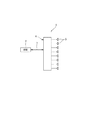
図1は、本発明の一実施形態に係るアレーアンテナシステムを備えた基地局装置の一部を示すブロック図である。図中、基地局装置1は、他の通信装置との間で無線通信を行う通信装置としての機能を有しており、ベースバンドユニット(BBU)2と、ベースバンドユニット2に信号伝送路(光伝送路または電気伝送路)3を介して接続されたアレーアンテナシステムとしてアクティブアンテナシステム4とを備えている。
[Details of the embodiment of the present invention]
Hereinafter, embodiments of the present invention will be described in detail with reference to the accompanying drawings.
<About base station equipment>
FIG. 1 is a block diagram showing a part of a base station apparatus provided with an array antenna system according to an embodiment of the present invention. In the figure, a base station apparatus 1 has a function as a communication apparatus that performs wireless communication with other communication apparatuses. A baseband unit (BBU) 2 and a signal transmission path ( An active antenna system 4 is provided as an array antenna system connected via an optical transmission path or an electrical transmission path 3.

ベースバンドユニット2は、無線通信によって送受信されるデータを含むベースバンド信号に対してデジタル変復調処理等の処理を行う機能を有しており、送信データを含むデジタルのベースバンド信号(I/Q信号)を信号伝送路3を介してアンテナシステム4に与える。
また、ベースバンドユニット2は、アンテナシステム4から信号伝送路3を介して与えられる、受信データを含んだデジタルのベースバンド信号(I/Q信号)を取得する。
The baseband unit 2 has a function of performing processing such as digital modulation / demodulation processing on a baseband signal including data transmitted and received by wireless communication, and a digital baseband signal (I / Q signal including transmission data). ) To the antenna system 4 via the signal transmission path 3.
Further, the baseband unit 2 acquires a digital baseband signal (I / Q signal) including received data, which is given from the antenna system 4 via the signal transmission path 3.

アクティブアンテナシステム4(以下、単にアンテナシステム4ともいう)は、無線周波数の信号を送受信するためのアンテナ素子5を複数(ここでは8個)備えており、基地局装置1が他の通信装置との間で無線通信を行う際に、当該無線通信に係る無線信号を送受信する機能を有している。
アンテナシステム4は、ベースバンドユニット2から与えられるデジタルのベースバンド信号に対して各種信号処理を行うことでアナログの無線周波数の信号に変換し、複数のアンテナ素子5から無線信号として送信する。
The active antenna system 4 (hereinafter also simply referred to as the antenna system 4) includes a plurality of (here, eight) antenna elements 5 for transmitting and receiving radio frequency signals, and the base station apparatus 1 is connected to other communication apparatuses. Have a function of transmitting and receiving a radio signal related to the wireless communication.
The antenna system 4 performs various signal processing on the digital baseband signal given from the baseband unit 2 to convert it into an analog radio frequency signal, and transmits it from the plurality of antenna elements 5 as a radio signal.

また、アンテナシステム4は、複数のアンテナ素子5が無線信号として受信する無線周波数の信号に対して各種信号処理を行うことでデジタルのベースバンド信号に変換し、変換したベースバンド信号をベースバンドユニット2に与える。   The antenna system 4 converts various radio frequency signals received as radio signals by the plurality of antenna elements 5 into digital baseband signals, and converts the converted baseband signals into baseband units. Give to 2.

このように、基地局装置1は、送信データを含んだベースバンド信号を無線周波数の信号に変換して他の通信装置に送信するとともに、他の通信装置が送信した無線周波数の信号を受信し、他の通信装置からの受信データを含んだベースバンド信号を取得する。   In this way, the base station apparatus 1 converts the baseband signal including the transmission data into a radio frequency signal and transmits it to another communication apparatus, and receives the radio frequency signal transmitted by the other communication apparatus. A baseband signal including received data from another communication device is acquired.

<アンテナシステムの構成について>
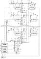
図2は、アンテナシステム4の送信側の構成を示すブロック図である。
アンテナシステム4は、デジタル信号処理部8と、アナログ信号処理部9とを備えている。
ベースバンドユニット2から無線通信のための送信信号としてアンテナシステム4に与えられるベースバンド信号は、デジタル信号処理部8によってデジタル信号処理された後、アナログ信号処理部9に与えられ、アナログの無線周波数の信号に変換されて各アンテナ素子5A〜5Hに与えられる。各アンテナ素子5A〜5Hに与えられたアナログの無線周波数の信号は、各アンテナ素子5A〜5Hから空間に放射され、無線信号として送信される。
<About the antenna system configuration>
FIG. 2 is a block diagram showing the configuration of the antenna system 4 on the transmission side.
The antenna system 4 includes a digital signal processing unit 8 and an analog signal processing unit 9.
The baseband signal given to the antenna system 4 as a transmission signal for wireless communication from the baseband unit 2 is subjected to digital signal processing by the digital signal processing unit 8 and then given to the analog signal processing unit 9 to obtain an analog radio frequency. And is given to each of the antenna elements 5A to 5H. Analog radio frequency signals given to the antenna elements 5A to 5H are radiated from the antenna elements 5A to 5H to the space and transmitted as radio signals.

デジタル信号処理部8は、CPUや、記憶部等を含んでいるコンピュータによって構成されており、記憶部に記憶されたプログラム等を読み出して以下に説明する当該デジタル信号処理部8が有する各機能部を実現するとともに各種処理を実行する機能を有している。
デジタル信号処理部8は、ベースバンドユニット2から与えられるベースバンド信号をアナログ信号処理部9に与える送信側の処理と、アナログ信号処理部9から与えられるベースバンド信号をベースバンドユニット2に与える受信側の処理とを行う機能を有している。
The digital signal processing unit 8 is configured by a computer including a CPU, a storage unit, and the like. Each functional unit included in the digital signal processing unit 8 described below by reading a program stored in the storage unit and the like is described below. And a function of executing various processes.
The digital signal processing unit 8 performs processing on the transmission side that gives the baseband signal given from the baseband unit 2 to the analog signal processing unit 9 and reception that gives the baseband signal given from the analog signal processing unit 9 to the baseband unit 2 Side processing.

アナログ信号処理部9は、デジタル信号処理部8から与えられるデジタルのベースバンド信号をアナログ信号に変換し、無線信号として送信するために必要なアナログ信号処理を行い、アナログ信号処理によって得られる無線周波数の信号をアンテナ素子5に与える機能を有している。
アナログ信号処理部9は、デジタル信号処理部8から与えられるデジタルのベースバンド信号をアナログに変換するデジタルアナログ変換器(DAC:Digital to Analog Converter)11を備えている。
また、アナログ信号処理部9は、デジタルアナログ変換器11からアンテナ素子5までの間に、アップコンバータ12と、電力分配器14と、複数の可変減衰器15と、複数の移相器16と、複数の電力増幅器(PA:Power Amplifier)17とを備えている。
The analog signal processing unit 9 converts the digital baseband signal given from the digital signal processing unit 8 into an analog signal, performs analog signal processing necessary for transmission as a radio signal, and obtains a radio frequency obtained by analog signal processing The signal is given to the antenna element 5.
The analog signal processing unit 9 includes a digital to analog converter (DAC) 11 that converts a digital baseband signal supplied from the digital signal processing unit 8 into analog.
The analog signal processing unit 9 includes an up-converter 12, a power distributor 14, a plurality of variable attenuators 15, a plurality of phase shifters 16, between the digital-analog converter 11 and the antenna element 5. A plurality of power amplifiers (PA) 17 are provided.

デジタルアナログ変換器11は、アナログに変換したベースバンド信号を後述するアップコンバータ12に与える。
アップコンバータ12は、発振器13が生成する無線周波数の局部発振信号をベースバンド信号に乗算することで、当該ベースバンド信号を無線周波数の信号に変換(アップコンバート)する機能を有している。アップコンバータ12は、ベースバンド信号を周波数変換することにより得た無線周波数信号を、後述する入力信号取出部18を通過して電力分配器14に与える。
電力分配器14は、無線周波数信号を複数のアンテナ素子5A〜5Hそれぞれに対応して複数に分配する。
The digital-analog converter 11 supplies the baseband signal converted into analog to an up-converter 12 described later.
The up-converter 12 has a function of converting (up-converting) the baseband signal into a radio frequency signal by multiplying the baseband signal by a radio frequency local oscillation signal generated by the oscillator 13. The up-converter 12 passes a radio frequency signal obtained by frequency-converting the baseband signal to the power distributor 14 through an input signal extraction unit 18 described later.
The power distributor 14 distributes the radio frequency signal into a plurality of pieces corresponding to the plurality of antenna elements 5A to 5H.

可変減衰器15には、電力分配器14によって分配された無線周波数信号が与えられる。可変減衰器15は、電力分配器14によって分配された無線周波数信号それぞれに対して利得を調整する。
移相器16には、可変減衰器15によって利得が調整された無線周波数信号が与えられる。複数の移相器16は、各可変減衰器15によって利得が調整された無線周波数信号それぞれに対して位相を個別に調整する。これによって、複数の移相器16は、複数のアンテナ素子5A〜5Hのそれぞれから送信される無線周波数信号のチルト角(指向性)を制御することができる。
The variable attenuator 15 is given the radio frequency signal distributed by the power distributor 14. The variable attenuator 15 adjusts the gain for each radio frequency signal distributed by the power distributor 14.
A radio frequency signal whose gain is adjusted by the variable attenuator 15 is given to the phase shifter 16. The plurality of phase shifters 16 individually adjust the phase for each radio frequency signal whose gain is adjusted by each variable attenuator 15. Accordingly, the plurality of phase shifters 16 can control the tilt angle (directivity) of the radio frequency signal transmitted from each of the plurality of antenna elements 5A to 5H.

電力増幅器17は、移相器16で位相が調整された無線周波数信号の電力を増幅する機能を有している。電力増幅器17は、増幅した無線周波数信号を、後述する出力信号取出部23及び反射信号取出部27を通過してアンテナ素子5に与える。電力増幅器17からアンテナ素子5に与えられた無線周波数信号は、アンテナ素子5から空間に放射され、無線信号として送信される。   The power amplifier 17 has a function of amplifying the power of the radio frequency signal whose phase is adjusted by the phase shifter 16. The power amplifier 17 passes the amplified radio frequency signal to the antenna element 5 through an output signal extraction unit 23 and a reflection signal extraction unit 27 described later. The radio frequency signal given from the power amplifier 17 to the antenna element 5 is radiated from the antenna element 5 to the space and transmitted as a radio signal.

可変減衰器15、移相器16、および電力増幅器17は、アンテナ素子5A〜5Hごとに設けられており、電力分配器14から各アンテナ素子5A〜5Hそれぞれに対応するように分配される無線周波数の送信信号に必要なアナログ処理を行う。   The variable attenuator 15, the phase shifter 16, and the power amplifier 17 are provided for each of the antenna elements 5A to 5H, and are distributed from the power distributor 14 so as to correspond to each of the antenna elements 5A to 5H. The analog processing necessary for the transmission signal is performed.

<アンテナシステムの制御構成について>
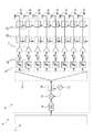
図3は、アンテナシステム4の制御構成を示すブロック図である。
アンテナシステム4は、主要な制御構成として、入力信号取出部18、基準移相器21、複数の出力信号取出部23、複数の反射信号取出部27、経路切替部29、合成器32、制御部40を備えている。
<Control configuration of antenna system>
FIG. 3 is a block diagram showing a control configuration of the antenna system 4.
The antenna system 4 includes an input signal extraction unit 18, a reference phase shifter 21, a plurality of output signal extraction units 23, a plurality of reflected signal extraction units 27, a path switching unit 29, a combiner 32, and a control unit as main control configurations. 40.

入力信号取出部18は、各移相器16への入力信号(無線周波数信号)を取り出す機能を有している。本実施形態における入力信号取出部18は、アップコンバータ12と電力分配器14との間に設けられており(図2参照)、アップコンバータ12で周波数変換された無線周波数信号を取り出すようになっている。   The input signal extraction unit 18 has a function of extracting an input signal (radio frequency signal) to each phase shifter 16. The input signal extraction unit 18 in the present embodiment is provided between the up converter 12 and the power distributor 14 (see FIG. 2), and extracts a radio frequency signal that has been frequency converted by the up converter 12. Yes.

入力信号取出部18から分岐した第1分岐線路51の途中には、さらに信号取出部20が設けられており、第1分岐線路51から信号取出部20により取り出された入力信号は基準移相器21に与えられる。   A signal extraction unit 20 is further provided in the middle of the first branch line 51 branched from the input signal extraction unit 18, and the input signal extracted from the first branch line 51 by the signal extraction unit 20 is a reference phase shifter. 21.

基準移相器21は、信号取出部20から分岐した第2分岐線路52の途中に設けられており、信号取出部20により取り出された入力信号の位相を設定する。基準移相器21により位相が設定された入力信号は、可変減衰器22に与えられ、この可変減衰器22によって利得が調整される。可変減衰器22により利得が調整された入力信号は合成器32(後述)に与えられる。なお、基準移相器21による具体的な位相の設定方法、及び可変減衰器22による具体的な利得の調整方法については後述する。   The reference phase shifter 21 is provided in the middle of the second branch line 52 branched from the signal extraction unit 20, and sets the phase of the input signal extracted by the signal extraction unit 20. The input signal whose phase is set by the reference phase shifter 21 is supplied to the variable attenuator 22, and the gain is adjusted by the variable attenuator 22. The input signal whose gain is adjusted by the variable attenuator 22 is supplied to a synthesizer 32 (described later). A specific phase setting method by the reference phase shifter 21 and a specific gain adjustment method by the variable attenuator 22 will be described later.

入力信号取出部18と信号取出部20との間には入力信号経路調整部19が設けられている。この入力信号経路調整部19は、入力信号取出部18から信号取出部20を介して合成器32に至るまでの経路長を調整するものである。
具体的には、入力信号経路調整部19は、合成器32における、入力信号の入力タイミングと、出力信号取出部23により取り出された出力信号の入力タイミングとを一致又は近似させるように前記経路長を調整するものである。
An input signal path adjustment unit 19 is provided between the input signal extraction unit 18 and the signal extraction unit 20. The input signal path adjustment unit 19 adjusts the path length from the input signal extraction unit 18 to the combiner 32 via the signal extraction unit 20.
Specifically, the input signal path adjustment unit 19 matches the path length so as to match or approximate the input timing of the input signal in the synthesizer 32 and the input timing of the output signal extracted by the output signal extraction unit 23. Is to adjust.

出力信号取出部23は、各移相器16から出力されて対応するアンテナ素子5に入力される出力信号(無線周波数信号)を取り出す機能を有している。本実施形態における複数の出力信号取出部23は、各電力増幅器17の後段であって、かつ対応するアンテナ素子5から一定距離だけ離れた位置に設けられている。
出力信号取出部23から分岐した第3分岐線路53には、第1切替部24、出力信号経路調整部25、信号取出部26がこの順に設けられている。第1切替部24、出力信号経路調整部25及び信号取出部26は、アンテナ素子5ごとに設けられている。
The output signal extraction unit 23 has a function of extracting an output signal (radio frequency signal) output from each phase shifter 16 and input to the corresponding antenna element 5. The plurality of output signal extraction units 23 in the present embodiment are provided in the subsequent stage of each power amplifier 17 and at a position away from the corresponding antenna element 5 by a certain distance.
The third branch line 53 branched from the output signal extraction unit 23 is provided with a first switching unit 24, an output signal path adjustment unit 25, and a signal extraction unit 26 in this order. The first switching unit 24, the output signal path adjustment unit 25, and the signal extraction unit 26 are provided for each antenna element 5.

第1切替部24は、例えばa接点、b接点及びc接点を有する3ポートスイッチよりなり、c接点をa接点及びb接点のいずれか一方の接点と接続するように切り替えるものである。
第1切替部24のc接点は出力信号取出部23に接続されている。また、第1切替部24のa接点は、抵抗24a及び平滑用のコンデンサ24bを介してグランドに接続されており、第1切替部24のb接点には出力信号経路調整部25が接続されている。
The first switching unit 24 includes, for example, a 3-port switch having an a contact, a b contact, and a c contact, and switches the c contact so as to be connected to one of the a contact and the b contact.
The contact c of the first switching unit 24 is connected to the output signal extraction unit 23. Further, the contact a of the first switching unit 24 is connected to the ground via a resistor 24a and a smoothing capacitor 24b, and the output signal path adjusting unit 25 is connected to the contact b of the first switching unit 24. Yes.

信号取出部26は、第3分岐線路53から出力信号を取り出す機能を有している。信号取出部26は、当該信号取出部26から分岐した第4分岐線路54を介して経路切替部29に接続されている。   The signal extraction unit 26 has a function of extracting an output signal from the third branch line 53. The signal extraction unit 26 is connected to the path switching unit 29 via a fourth branch line 54 branched from the signal extraction unit 26.

出力信号経路調整部25は、各出力信号取出部23から信号取出部26、第4分岐線路54、経路切替部29、後述するサーキュレータ30及び第6分岐線路56を介して合成器32に至る経路長を調整するものである。
具体的には、出力信号経路調整部25は、各出力信号取出部23から合成器32までの複数の前記経路長同士の差分が、使用周波数の波長の整数倍の長さとなるように、前記各経路長を個別に調整するものである。
The output signal path adjustment unit 25 is a path from each output signal extraction unit 23 to the combiner 32 via the signal extraction unit 26, the fourth branch line 54, the path switching unit 29, a circulator 30 and a sixth branch line 56 described later. The length is adjusted.
Specifically, the output signal path adjustment unit 25 is configured so that the difference between the plurality of path lengths from each output signal extraction unit 23 to the synthesizer 32 is an integral multiple of the wavelength of the used frequency. Each path length is adjusted individually.

反射信号取出部27は、各移相器16から対応するアンテナ素子5に至る経路において当該アンテナ素子5からの反射信号を取り出す機能を有している。本実施形態における反射信号取出部27は、反射波(反射信号)を取り出す方向性結合器によって構成されており、各アンテナ素子5の手前に設けられている。
反射信号取出部27から分岐した第5分岐線路55の途中には、第2切替部28が設けられている。この第2切替部28はアンテナ素子5ごとに設けられている。
The reflected signal extraction unit 27 has a function of extracting a reflected signal from the antenna element 5 in a path from each phase shifter 16 to the corresponding antenna element 5. The reflected signal extraction unit 27 in the present embodiment is configured by a directional coupler that extracts a reflected wave (reflected signal), and is provided in front of each antenna element 5.
A second switching unit 28 is provided in the middle of the fifth branch line 55 branched from the reflected signal extraction unit 27. The second switching unit 28 is provided for each antenna element 5.

第2切替部28は、例えばa接点、b接点及びc接点を有する3ポートスイッチよりなり、c接点をa接点及びb接点のいずれか一方の接点と接続するように切り替えるものである。
第2切替部28のc接点は反射信号取出部27に接続されている。また、第2切替部28のa接点は、抵抗28a及び平滑用のコンデンサ28bを介してグランドに接続されており、第2切替部28のb接点は第5分岐線路55を介して経路切替部29に接続されている。
The 2nd switching part 28 consists of 3 port switches which have a contact, b contact, and c contact, for example, and switches c contact so that either a contact or a contact may be connected.
The c contact point of the second switching unit 28 is connected to the reflected signal extraction unit 27. The contact a of the second switching unit 28 is connected to the ground via the resistor 28a and the smoothing capacitor 28b, and the contact b of the second switching unit 28 is connected to the path switching unit via the fifth branch line 55. 29.

経路切替部29は、下記の第1経路〜第3経路のうちのいずれかの経路に切り替えるものである。
第1経路:出力信号取出部23と合成器32とを電気的に接続するための経路
第2経路:反射信号取出部27と合成器32とを電気的に接続するための経路
第3経路:入力信号取出部18と複数の出力信号経路調整部25とを電気的に接続するための経路
The route switching unit 29 switches to any one of the following first route to third route.
First path: path for electrically connecting the output signal extraction unit 23 and the synthesizer 32 Second path: path for electrically connecting the reflected signal extraction unit 27 and the synthesizer 32 Third path: A path for electrically connecting the input signal extraction unit 18 and the plurality of output signal path adjustment units 25

本実施形態の経路切替部29は、例えばa接点、b接点、c接点及びd接点を有する4ポートスイッチよりなり、d接点をa接点〜c接点のいずれかの接点と接続するように切り替えるものである。
経路切替部29のa接点は、第3分岐線路53上の図中最下部に配置された信号取出部26に接続されている。また、経路切替部29のb接点には第4分岐線路54が接続され、経路切替部29のc接点には第5分岐線路55が接続されている。
The path switching unit 29 of the present embodiment includes, for example, a 4-port switch having an a contact, a b contact, a c contact, and a d contact, and switches so that the d contact is connected to any one of the contacts a to c. It is.
The contact a of the path switching unit 29 is connected to the signal extraction unit 26 disposed at the bottom of the third branch line 53 in the drawing. The fourth branch line 54 is connected to the b contact of the path switching unit 29, and the fifth branch line 55 is connected to the c contact of the path switching unit 29.

経路切替部29のd接点は、サーキュレータ30に接続されている。このサーキュレータ30は、第1分岐線路51上において信号取出部20の後段に設けられている。
サーキュレータ30は、第1分岐線路51側から入力された信号を経路切替部29のd接点側に出力し、経路切替部29のd接点側から入力された信号を第6分岐線路56に出力する。
The contact d of the path switching unit 29 is connected to the circulator 30. The circulator 30 is provided on the first branch line 51 after the signal extraction unit 20.
The circulator 30 outputs a signal input from the first branch line 51 side to the d contact side of the path switching unit 29, and outputs a signal input from the d contact side of the path switching unit 29 to the sixth branch line 56. .

第6分岐線路56は、サーキュレータ30と合成器32とを電気的に接続している。第6分岐線路56の途中には可変減衰器31が設けられている。可変減衰器31は、サーキュレータ30から第6分岐線路56に出力された信号(出力信号又は反射信号)の利得を調整する。可変減衰器31により利得が調整された信号は合成器32に与えられる。   The sixth branch line 56 electrically connects the circulator 30 and the synthesizer 32. A variable attenuator 31 is provided in the middle of the sixth branch line 56. The variable attenuator 31 adjusts the gain of the signal (output signal or reflected signal) output from the circulator 30 to the sixth branch line 56. The signal whose gain is adjusted by the variable attenuator 31 is supplied to the synthesizer 32.

以上の構成により、経路切替部29がb接点に接続された場合は、出力信号取出部23と合成器32とを接続可能な上記第1経路となる。また、経路切替部29がc接点に接続された場合は、反射信号取出部27と合成器32とを電気的に接続可能な上記第2経路となる。さらに、経路切替部29がa接点に接続された場合は、入力信号取出部18と複数の出力信号経路調整部25とを電気的に接続可能な上記第3経路となる。   With the above configuration, when the path switching unit 29 is connected to the b-contact, the first path can be connected to the output signal extraction unit 23 and the combiner 32. Further, when the path switching unit 29 is connected to the c contact, the second path can be electrically connected to the reflected signal extraction unit 27 and the combiner 32. Further, when the path switching unit 29 is connected to the contact a, the third path can be electrically connected to the input signal extraction unit 18 and the plurality of output signal path adjustment units 25.

合成器32は、経路切替部29がb接点に接続されている場合には、基準移相器21により位相が設定された入力信号と、出力信号取出部23により取り出された出力信号とを合成する。
また、合成器32は、経路切替部29がc接点に接続されている場合には、基準移相器21により位相が設定された入力信号と、反射信号取出部27により取り出された反射信号とを合成する。
The synthesizer 32 synthesizes the input signal whose phase is set by the reference phase shifter 21 and the output signal extracted by the output signal extraction unit 23 when the path switching unit 29 is connected to the b-contact. To do.
In addition, when the path switching unit 29 is connected to the c contact, the synthesizer 32 includes the input signal whose phase is set by the reference phase shifter 21 and the reflected signal extracted by the reflected signal extracting unit 27. Is synthesized.

合成器32の後段には、当該合成器32により2つの信号を合成したときの合成信号の状態を検出する信号状態検出部33が設けられている。
本実施形態における信号状態検出部33は、例えば検波ダイオードよりなり、入力された合成信号の電圧を検出するものである。なお、信号状態検出部33は、検波ダイオード以外に、スペクトラムアナライザなど、上記合成信号の状態を検出できるものであれば他の検出器を用いても良い。
A signal state detection unit 33 that detects the state of the combined signal when the two signals are combined by the combiner 32 is provided at the subsequent stage of the combiner 32.
The signal state detection unit 33 in the present embodiment is made up of, for example, a detection diode, and detects the voltage of the input composite signal. In addition to the detection diode, the signal state detection unit 33 may use another detector, such as a spectrum analyzer, as long as it can detect the state of the synthesized signal.

制御部40は、CPU及び記憶部43等を含んでいるコンピュータによって構成されており、記憶部43に記憶されたコンピュータプログラム等を読み出して以下に説明する当該制御部40が有する各機能部を実現するとともに各種処理を実行する機能を有している。   The control unit 40 is configured by a computer including a CPU and a storage unit 43. The control unit 40 reads out a computer program or the like stored in the storage unit 43 and realizes each functional unit included in the control unit 40 described below. And has a function of executing various processes.

制御部40は、ベースバンドユニット2に接続されており、ベースバンドユニット2からアンテナ素子5から送信する信号のチルト角を設定する制御命令や搬送波周波数を含む制御情報を受ける。
制御部40は、上記コンピュータプログラムを実行することで達成される機能部として、位相制御部41と判定部42とを有する。
The control unit 40 is connected to the baseband unit 2 and receives control information including a control command for setting a tilt angle of a signal transmitted from the antenna element 5 from the baseband unit 2 and a carrier frequency.
The control unit 40 includes a phase control unit 41 and a determination unit 42 as functional units achieved by executing the computer program.

位相制御部41は、各アンテナ素子5に入力される出力信号の位相が所望の位相となるように基準移相器21及び対応する移相器16等を制御するものである。
具体的には、位相制御部41は、取り出された入力信号の位相が所望の位相の逆位相となるように基準移相器21を制御する。そして、位相制御部41は、基準移相器21により位相が設定された入力信号と、出力信号取出部23から取り出された出力信号とを合成器32により合成するときに、これらの両信号が互いに相殺されるように、検波ダイオード33が検出する電圧値に応じて、対応する移相器16を制御する。
The phase control unit 41 controls the reference phase shifter 21 and the corresponding phase shifter 16 so that the phase of the output signal input to each antenna element 5 becomes a desired phase.
Specifically, the phase control unit 41 controls the reference phase shifter 21 so that the phase of the extracted input signal is opposite to the desired phase. Then, when the phase control unit 41 combines the input signal whose phase is set by the reference phase shifter 21 and the output signal extracted from the output signal extraction unit 23 by the combiner 32, both these signals are The corresponding phase shifter 16 is controlled in accordance with the voltage value detected by the detection diode 33 so as to cancel each other.

また、位相制御部41は、各移相器16に対応する可変減衰器15、他の可変減衰器22,31、第1切替部24、第2切替部28、及び経路切替部29も個別に制御する。これらの具体的な制御については後述する。
本実施形態では、移相器16、入力信号取出部18、出力信号取出部23、基準移相器21、合成器32、及び位相制御部41を主要な構成要素として位相制御装置が構成されている。
The phase control unit 41 also includes the variable attenuator 15 corresponding to each phase shifter 16, the other variable attenuators 22, 31, the first switching unit 24, the second switching unit 28, and the path switching unit 29 individually. Control. These specific controls will be described later.
In this embodiment, the phase control device is configured with the phase shifter 16, the input signal extraction unit 18, the output signal extraction unit 23, the reference phase shifter 21, the synthesizer 32, and the phase control unit 41 as main components. Yes.

判定部42は、位相制御部41が移相器16等を制御した後に、当該移相器16に対応するアンテナ素子5から送信される信号の位相異常の有無を判定するものである。
その際、判定部42は、反射信号取出部27により取り出された各アンテナ素子5からの反射信号に基づいて前記位相異常の有無を判定する。
The determination unit 42 determines whether or not there is a phase abnormality in a signal transmitted from the antenna element 5 corresponding to the phase shifter 16 after the phase control unit 41 controls the phase shifter 16 or the like.
At that time, the determination unit 42 determines the presence / absence of the phase abnormality based on the reflection signal from each antenna element 5 extracted by the reflection signal extraction unit 27.

本実施形態における判定部42は、過去の反射信号に基づく情報と、現在の反射信号に基づく情報とに基づいて、前記位相異常の有無を判定する。
具体的には、判定部42は、工場出荷時において合成器32が入力信号と反射信号とを合成した合成信号の電圧値と、現時点において合成器32により入力信号と反射信号とを合成した合成信号の電圧値とのずれ量に応じて、前記位相異常の有無を判定する。なお、工場出荷時における上記合成信号の電圧値は、記憶部43に記憶されている。
The determination unit 42 in the present embodiment determines the presence / absence of the phase abnormality based on information based on past reflected signals and information based on current reflected signals.
Specifically, the determination unit 42 combines the voltage value of the combined signal obtained by combining the input signal and the reflected signal by the combiner 32 at the time of factory shipment, and the combined signal obtained by combining the input signal and the reflected signal at the present time. The presence / absence of the phase abnormality is determined according to the amount of deviation from the voltage value of the signal. Note that the voltage value of the combined signal at the time of factory shipment is stored in the storage unit 43.

判定部42は、前記位相異常が有ると判定した場合、その判定結果を報知する指令を出力する。この報知指令が判定部42から出力されると、例えばアンテナ素子5の設置現場又は基地局に設けられた警告ランプ等を点灯させることで、位相異常が生じたことをオペレータ等に報知することができる。   If it is determined that the phase abnormality is present, the determination unit 42 outputs a command for informing the determination result. When this notification command is output from the determination unit 42, for example, an alarm lamp or the like provided at the installation site of the antenna element 5 or the base station is turned on to notify the operator or the like that a phase abnormality has occurred. it can.

なお、判定部42は、上記ずれ量の程度に応じて、位相異常の度合いを判定しても良い。例えば、判定部42は、上記ずれ量が小さい場合には、位相異常の度合いは低いと判定して上記報知指令の出力を行わずに判定を終了し、上記ずれ量が大きい場合には、位相異常の度合いが高いと判定して上記報知指令の出力を行うようにしても良い。
本実施形態では、反射信号取出部27及び判定部42を主要な構成要素として、アンテナ素子5から送信される信号の位相異常を検出する位相異常検出装置が構成されている。
Note that the determination unit 42 may determine the degree of phase abnormality in accordance with the degree of deviation. For example, when the deviation amount is small, the determination unit 42 determines that the degree of phase abnormality is low and ends the determination without outputting the notification command. When the deviation amount is large, the determination unit 42 It may be determined that the degree of abnormality is high and the notification command is output.
In the present embodiment, a phase abnormality detection device that detects a phase abnormality of a signal transmitted from the antenna element 5 is configured with the reflected signal extraction unit 27 and the determination unit 42 as main components.

<制御部が実行する制御について>
次に、制御部40が実行する制御について、図4〜図8を参照しながら説明する。なお、ここでは、アンテナシステム4の工場出荷時に行う制御から説明する。
<出力信号の経路調整の確認工程>
まず、工場出荷時において、制御部40は、各出力信号取出部23から合成器32までの複数の経路長同士の差分が、使用周波数の波長の整数倍の長さとなるように、各出力信号経路調整部25が適切に調整されているか否かを確認する。具体的には、図4に示すように、制御部40は、複数の第1切替部24をすべてb接点に接続するように切り替えるとともに、経路切替部29をa接点に接続させた第3経路に切り替える。これにより、入力信号取出部18と複数の出力信号経路調整部25とが直列に接続された状態となる。
<Control executed by the control unit>
Next, control executed by the control unit 40 will be described with reference to FIGS. Here, the control performed at the time of factory shipment of the antenna system 4 will be described.
<Output signal path adjustment confirmation process>
First, at the time of factory shipment, the control unit 40 sets each output signal so that a difference between a plurality of path lengths from each output signal extraction unit 23 to the synthesizer 32 is an integral multiple of the wavelength of the used frequency. It is confirmed whether or not the route adjustment unit 25 is appropriately adjusted. Specifically, as shown in FIG. 4, the control unit 40 switches the plurality of first switching units 24 so as to connect all the first switching units 24 to the b contact, and also connects the path switching unit 29 to the a contact. Switch to. As a result, the input signal extraction unit 18 and the plurality of output signal path adjustment units 25 are connected in series.

次に、制御部40は、図中の最も上側に配置された第1切替部24をa接点に切り替える。これにより、入力信号取出部18により取り出された入力信号の一部は、第1分岐線路51及び経路切替部29を経て第3分岐線路53上において図中の最も上側に配置された第1切替部24のb接点で反射して折り返す。この折り返し信号は、第3分岐線路53上の全ての出力信号経路調整部25を通過した後、経路切替部29、サーキュレータ30、及び第6分岐線路56を経て合成器32に入力される。
また、入力信号取出部18により取り出された入力信号の他部は、第3分岐線路53上の信号取出部20及び第2分岐線路52を経て合成器32に入力される。
Next, the control part 40 switches the 1st switching part 24 arrange | positioned at the uppermost side in a figure to a contact. Thereby, a part of the input signal extracted by the input signal extraction unit 18 passes through the first branch line 51 and the path switching unit 29, and the first switching is arranged on the uppermost side in the drawing on the third branch line 53. Reflected at the b-contact of the part 24 and folded. The folded signal passes through all output signal path adjustment units 25 on the third branch line 53, and then is input to the synthesizer 32 through the path switching unit 29, the circulator 30, and the sixth branch line 56.
The other part of the input signal extracted by the input signal extraction unit 18 is input to the combiner 32 via the signal extraction unit 20 and the second branch line 52 on the third branch line 53.

次に、制御部40は、合成器32により上記折り返し信号と入力信号の他部とを合成した信号の電圧値を検波ダイオード33から取得し、その電圧値に応じて合成器32に入力される両信号を相殺するように基準移相器21を制御する。そして、制御部40は、その両信号が相殺されたときの基準移相器21の制御電圧値を第1相殺条件として記憶部に43に記憶する。   Next, the control unit 40 acquires the voltage value of the signal obtained by synthesizing the folded signal and the other part of the input signal from the synthesizer 32 from the detection diode 33 and inputs the voltage value to the synthesizer 32 according to the voltage value. The reference phase shifter 21 is controlled so as to cancel both signals. And the control part 40 memorize | stores in the memory | storage part 43 the control voltage value of the reference | standard phase shifter 21 when the both signals are canceled as 1st cancellation conditions.

次に、制御部40は、図中の上から2番目の第1切替部24をa接点に切り替える。これにより、入力信号取出部18により取り出された入力信号の一部は、第1分岐線路51及び経路切替部29を経て第3分岐線路53上において図中の上から2番目の第1切替部24のb接点で反射して折り返す。この折り返し信号は、第3分岐線路53上において図中の最も上側に配置された出力信号経路調整部25を除く全ての出力信号経路調整部25を通過した後、経路切替部29、サーキュレータ30及び第6分岐線路56を経て合成器32に入力される。
また、入力信号取出部18により取り出された入力信号の他部は、第3分岐線路53上の信号取出部20、第2分岐線路52を経て合成器32に入力される。
Next, the control part 40 switches the 2nd 1st switching part 24 from the top in a figure to a contact. As a result, a part of the input signal extracted by the input signal extraction unit 18 passes through the first branch line 51 and the path switching unit 29, and then the second first switching unit from the top in the figure on the third branch line 53. Reflected at b contact of 24 and folded. The folded signal passes through all the output signal path adjustment units 25 except for the output signal path adjustment unit 25 arranged on the uppermost side in the drawing on the third branch line 53, and then the path switching unit 29, the circulator 30 and the The signal is input to the synthesizer 32 via the sixth branch line 56.
The other part of the input signal extracted by the input signal extraction unit 18 is input to the synthesizer 32 via the signal extraction unit 20 and the second branch line 52 on the third branch line 53.

次に、制御部40は、合成器32により上記折り返し信号と入力信号の他部とを合成した信号の電圧値を検波ダイオード33から取得し、その電圧値に応じて合成器32に入力される両信号を相殺するように基準移相器21を制御する。そして、制御部40は、その両信号が相殺されたときの基準移相器21の制御電圧値を第2相殺条件として記憶部に43に記憶する。   Next, the control unit 40 acquires the voltage value of the signal obtained by synthesizing the folded signal and the other part of the input signal from the synthesizer 32 from the detection diode 33 and inputs the voltage value to the synthesizer 32 according to the voltage value. The reference phase shifter 21 is controlled so as to cancel both signals. And the control part 40 memorize | stores in the memory | storage part 43 the control voltage value of the reference | standard phase shifter 21 when the both signals are canceled as 2nd cancellation conditions.

次に、制御部40は、記憶部43に記憶した上記第1相殺条件の制御電圧値と上記第2相殺条件の制御電圧値とに基づいて、両相殺条件における基準移相器21の位相が360度ずれた関係にあるか否かを判定する。この判定は、例えば、予め記憶部43に記憶された、制御電圧値と位相との関係を示すルックアップテーブルを用いて行うことができる。
このようにして、制御部40は、残りの第1切替部24についても、順にa接点に切り替えることによって、上記と同様の判定を行う。なお、制御部40は、上記いずれかの判定結果が否定的である場合には、その判定結果を報知する指令を出力するようにすれば良い。
Next, based on the control voltage value of the first cancellation condition and the control voltage value of the second cancellation condition stored in the storage unit 43, the control unit 40 determines the phase of the reference phase shifter 21 in both cancellation conditions. It is determined whether or not the relationship is shifted by 360 degrees. This determination can be performed using, for example, a lookup table that is stored in advance in the storage unit 43 and indicates the relationship between the control voltage value and the phase.
In this way, the control unit 40 performs the same determination as described above by sequentially switching the remaining first switching unit 24 to the a contact. In addition, what is necessary is just to make it the control part 40 output the instruction | command which alert | reports the determination result, when one of the said determination results is negative.

<各アンテナ素子に対応する移相器の制御工程>
上記の各出力信号の経路調整の確認工程が終了すると、続いて制御部40は、複数のアンテナ素子5A〜5Hに入力される出力信号の位相が所望の位相となるように、対応する移相器16等を制御する。
例えば、制御部40は、ベースバンドユニット2からアンテナ素子5Aに入力される出力信号の位相を10°に設定する制御命令を受けた場合、まず、入力信号取出部18から取り出された入力信号の位相が上記制御命令の位相(10°)の逆位相である190°又は−170°となるように、基準移相器21の制御電圧を制御する。その際、制御部40は、制御電圧値と位相との関係を示す上記ルックアップテーブルを用いて基準移相器21の制御電圧を制御する。
<Control process of phase shifter corresponding to each antenna element>
When the above-described process of confirming the path adjustment of each output signal is completed, the control unit 40 subsequently shifts the corresponding phase shift so that the phase of the output signal input to the plurality of antenna elements 5A to 5H becomes a desired phase. The device 16 is controlled.
For example, when the control unit 40 receives a control command for setting the phase of the output signal input to the antenna element 5A from the baseband unit 2 to 10 °, first, the control unit 40 first extracts the input signal extracted from the input signal extraction unit 18. The control voltage of the reference phase shifter 21 is controlled so that the phase becomes 190 ° or −170 ° which is the opposite phase of the phase (10 °) of the control command. At that time, the control unit 40 controls the control voltage of the reference phase shifter 21 using the lookup table indicating the relationship between the control voltage value and the phase.

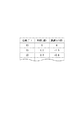
また、上記制御命令の位相に応じて基準移相器21による入力信号の通過ロスが変化するので、制御部40は、その通過ロスが一定となるように可変減衰器22を制御する。この制御は、例えば、図5に示すように、各位相とこれに対応する利得及び通過ロスとの関係を示すルックアップテーブルを用いて行うことができる。
ここでは、上記制御命令の位相は10°なので、制御部40は、図5のルックアップテーブルを参照して、位相が10°の場合における通過ロス(−1.5dB)を相殺するように、入力信号の利得が1.5dBとなるように可変減衰器22を制御する。
Further, since the passage loss of the input signal by the reference phase shifter 21 changes according to the phase of the control command, the control unit 40 controls the variable attenuator 22 so that the passage loss becomes constant. For example, as shown in FIG. 5, this control can be performed using a look-up table indicating the relationship between each phase and the corresponding gain and pass loss.
Here, since the phase of the control command is 10 °, the control unit 40 refers to the lookup table of FIG. 5 so as to cancel out the passage loss (−1.5 dB) when the phase is 10 °. The variable attenuator 22 is controlled so that the gain of the input signal is 1.5 dB.

次に、図6において、制御部40は、アンテナ5Aに対応する、図中の最も上側に配置された移相器16及び可変減衰器15を制御する。具体的には、制御部40は、経路切替部29をb接点に接続させた第1経路に切り替えるとともに、図中の最も上側に配置された第1切替部24をb接点に接続するように切り替える。なお、他の第1切替部24は全てa接点に接続されている。   Next, in FIG. 6, the control unit 40 controls the phase shifter 16 and the variable attenuator 15 disposed on the uppermost side in the figure corresponding to the antenna 5 </ b> A. Specifically, the control unit 40 switches the path switching unit 29 to the first path connected to the b contact, and connects the first switching unit 24 arranged on the uppermost side in the drawing to the b contact. Switch. The other first switching units 24 are all connected to the a contact.

これにより、図中の最も上側に配置された出力信号取出部23から取り出された出力信号は、その後段直後に配置された第1切替部24、出力信号経路調整部25及び信号取出部26を経て第4分岐線路54に取り出される。そして、第4分岐線路54に取り出された出力信号は、経路切替部29、サーキュレータ30及び第6分岐線路56を経て合成器32に入力される。
したがって、合成器32では、基準移相器21により位相が設定された入力信号と、図中の最も上側に配置された出力信号取出部23から取り出された出力信号とが合成される。
As a result, the output signal taken out from the output signal take-out unit 23 arranged at the uppermost position in the figure is passed through the first switching unit 24, the output signal path adjusting unit 25 and the signal take-out unit 26 arranged immediately after the subsequent stage. Then, it is taken out to the fourth branch line 54. Then, the output signal extracted to the fourth branch line 54 is input to the combiner 32 via the path switching unit 29, the circulator 30 and the sixth branch line 56.
Therefore, the synthesizer 32 synthesizes the input signal whose phase is set by the reference phase shifter 21 and the output signal extracted from the output signal extraction unit 23 arranged on the uppermost side in the drawing.

次に、制御部40は、合成器32に入力された入力信号と出力信号とが合成されるときに、これらの両信号が互いに相殺されるように、検波ダイオード33が検出する電圧値に応じて、図中の最も上側に配置された移相器16を制御する。その際、移相器16により出力信号の位相が変化することで、当該移相器16を通過する出力信号の利得も変化するので、制御部40は、当該移相器16の前段に配置された可変減衰器15も制御する。   Next, when the input signal input to the combiner 32 and the output signal are combined, the control unit 40 responds to the voltage value detected by the detection diode 33 so that these two signals cancel each other. Thus, the phase shifter 16 arranged on the uppermost side in the figure is controlled. At this time, since the phase of the output signal is changed by the phase shifter 16, the gain of the output signal passing through the phase shifter 16 is also changed. Therefore, the control unit 40 is arranged in the previous stage of the phase shifter 16. The variable attenuator 15 is also controlled.

具体的には、制御部40は、まず、移相器16及び可変減衰器15を制御する前の初期状態において検波ダイオード33で検出される合成信号の電圧値V(図7(A)参照)を記憶部43に記憶する。
次に、制御部40は、検波ダイオード33で検出される電圧値を最小化させるように移相器16及び可変減衰器15の制御電圧をそれぞれ少しずつ変化させ、その制御電圧を変化させたときに検波ダイオード33が検出した電圧値V(図7(B)参照)を取得する。
Specifically, the control unit 40 firstly determines the voltage value V 0 of the combined signal detected by the detection diode 33 in the initial state before controlling the phase shifter 16 and the variable attenuator 15 (see FIG. 7A). ) Is stored in the storage unit 43.
Next, when the control unit 40 changes the control voltage of the phase shifter 16 and the variable attenuator 15 little by little so as to minimize the voltage value detected by the detection diode 33, the control voltage is changed. The voltage value V 1 (see FIG. 7B) detected by the detection diode 33 is acquired.

そして、制御部40は、取得した電圧値V1が初期状態の電圧値Vに対して閾値以上低減しているか否かを判定する。本実施形態では、例えば使用周波数を3.5GHzとした場合、取得した電圧値が初期状態の電圧値に対して25dB以上低減しているか否かを判定する。25dB以上低減していることは、合成器32により合成される両信号は、位相の誤差が±5°以内であって且つ通過利得の誤差が±0.5dB以内の同じ大きさの信号となって、両信号が互いに逆位相で相殺されることを意味する。 Then, the control unit 40 determines whether the acquired voltage value V 1 is being reduced threshold above the voltage value V 0 which initial state. In this embodiment, for example, when the use frequency is 3.5 GHz, it is determined whether or not the acquired voltage value is reduced by 25 dB or more with respect to the voltage value in the initial state. The reduction of 25 dB or more means that both signals synthesized by the synthesizer 32 are signals of the same magnitude with a phase error within ± 5 ° and a passing gain error within ± 0.5 dB. This means that both signals cancel each other out of phase.

したがって、制御部40は、上記判定結果が肯定的である場合には、合成器32により合成される両信号は相殺されるので、図6中の最も上側に配置された移相器16及び可変減衰器15の制御を終了する。そして、制御部40は、対応する第1切替部24をa接点に接続するように切り替える。
一方、制御部40は、上記判定結果が否定的である場合には、上記判定結果が肯定的になるまで、移相器16及び可変減衰器15の制御電圧を変化させる制御と上記判定とを繰り返し行う。
Therefore, when the determination result is affirmative, the control unit 40 cancels both signals synthesized by the synthesizer 32, so that the phase shifter 16 arranged on the uppermost side in FIG. The control of the attenuator 15 is finished. And the control part 40 switches so that the corresponding 1st switching part 24 may be connected to a contact.
On the other hand, if the determination result is negative, the control unit 40 performs control for changing the control voltage of the phase shifter 16 and the variable attenuator 15 and the determination until the determination result becomes positive. Repeat.

上記制御により、合成器32によって合成される出力信号は、当該出力信号と合成される入力信号に対して逆位相、すなわち上記制御命令の位相と同位相となるように調整される。その結果、上記移相器16から出力された出力信号は、その位相が上記制御命令の位相(ここでは10°)となってアンテナ素子5Aから送信される。したがって、通信中においてアンテナ素子5から送信される信号の位相を所望の位相に調整することができる。
また、制御部40は、移相器16と共に可変減衰器15を制御するので、通信中においてアンテナ素子5Aから送信される信号の利得も調整することができる。
By the above control, the output signal synthesized by the synthesizer 32 is adjusted so as to have an opposite phase to the input signal synthesized with the output signal, that is, the same phase as the phase of the control command. As a result, the output signal output from the phase shifter 16 is transmitted from the antenna element 5A with the phase thereof being the phase of the control command (here, 10 °). Therefore, the phase of the signal transmitted from the antenna element 5 during communication can be adjusted to a desired phase.
Moreover, since the control part 40 controls the variable attenuator 15 with the phase shifter 16, it can also adjust the gain of the signal transmitted from the antenna element 5A during communication.

上記のようにアンテナ素子5Aに対応する移相器16等の制御が終了すると、制御部40は、他のアンテナ素子5B〜5Hに入力される出力信号の位相についても、それぞれ所望の位相となるように、上記と同様の方法により基準移相器21及び対応する移相器16等を用いて順次設定する。
その際、各アンテナ素子5B〜5Hに対応する出力信号取出部23から取り出された出力信号が合成器32に入力されるときの位相がばらばらであると、図7(B)〜図7(D)に示すように、合成器32に入力された入力信号と出力信号とを相殺するときの電圧波形もばらばらとなる。
When the control of the phase shifter 16 and the like corresponding to the antenna element 5A is completed as described above, the control unit 40 also sets the phases of the output signals input to the other antenna elements 5B to 5H to desired phases, respectively. As described above, the reference phase shifter 21 and the corresponding phase shifter 16 are sequentially set by the same method as described above.
At this time, if the output signals extracted from the output signal extraction units 23 corresponding to the antenna elements 5B to 5H are input to the synthesizer 32, the phases vary, as shown in FIGS. 7B to 7D. ), The voltage waveform when the input signal input to the synthesizer 32 and the output signal are offset also varies.

これに対して、本実施形態では、各アンテナ素子5A〜5Hに対応する上記の経路長同士の差分は、各出力信号経路調整部25により使用周波数の波長の整数倍の長さとなるように調整されている。このため、各アンテナ素子5A〜5Hに対応する移相器16等を制御する際に、合成器32に入力された入力信号と出力信号とを相殺するときの電圧波形を例えば図7(B)に示す電圧波形に近似させることができる。したがって、両信号を相殺する条件を近似させることができるので、各アンテナ素子5A〜5Hに対応する移相器16等を容易に調整することができる。   On the other hand, in the present embodiment, the difference between the path lengths corresponding to each of the antenna elements 5A to 5H is adjusted by each output signal path adjustment unit 25 to be a length that is an integral multiple of the wavelength of the operating frequency. Has been. For this reason, when controlling the phase shifter 16 etc. corresponding to each antenna element 5A-5H, the voltage waveform when the input signal input into the combiner 32 and an output signal are canceled is shown in FIG. Can be approximated to the voltage waveform shown in FIG. Therefore, since the conditions for canceling both signals can be approximated, the phase shifter 16 and the like corresponding to each of the antenna elements 5A to 5H can be easily adjusted.

また、入力信号取出部18を通過して各出力信号取出部23により取り出される出力信号は、その出力信号取出部23の前段に設けられた電力増幅器17等を通過するため、合成器32に入力される出力信号の入力タイミングは、入力信号の入力タイミングよりも遅くなる。
これに対して、本実施形態では、合成器32における入力信号の入力タイミングと出力信号の入力タイミングとを一致又は近似させるように、入力信号取出部18から合成器32までの経路長を調整する入力信号経路調整部19を第1分岐線路51に設けている。このため、入力信号経路調整部19により、合成器32における入力信号の入力タイミングと出力信号の入力タイミングとを一致又は近似させることができるので、各アンテナ素子5A〜5Hに対応する移相器16等をさらに容易に調整することができる。
Further, the output signals that pass through the input signal extraction unit 18 and are extracted by the output signal extraction units 23 pass through the power amplifier 17 and the like provided in the preceding stage of the output signal extraction unit 23, and are thus input to the combiner 32. The input timing of the output signal is later than the input timing of the input signal.
In contrast, in the present embodiment, the path length from the input signal extraction unit 18 to the synthesizer 32 is adjusted so that the input timing of the input signal and the input timing of the output signal in the synthesizer 32 match or approximate. The input signal path adjustment unit 19 is provided in the first branch line 51. For this reason, the input signal path adjustment unit 19 can match or approximate the input timing of the input signal and the input timing of the output signal in the synthesizer 32, so the phase shifters 16 corresponding to the antenna elements 5 </ b> A to 5 </ b> H. Etc. can be adjusted more easily.

<各アンテナ素子からの反射信号の状態確認工程>
上記の各アンテナ素子5A〜5Hに対応する移相器16の制御工程が終了すると、続いて制御部40は、各アンテナ素子5A〜5Hからの反射信号の状態を確認する。
具体的には、図8に示すように、制御部40は、経路切替部29をc接点に接続させた第2経路に切り替えるとともに、図中の最も上側に配置された第2切替部28をb接点に接続するように切り替える。なお、他の第2切替部28は全てa接点に接続されている。
<Confirmation process of reflected signal from each antenna element>
When the control process of the phase shifter 16 corresponding to each of the antenna elements 5A to 5H is completed, the control unit 40 confirms the state of the reflected signal from each of the antenna elements 5A to 5H.
Specifically, as shown in FIG. 8, the control unit 40 switches the path switching unit 29 to the second path connected to the c contact, and the second switching unit 28 arranged on the uppermost side in the figure. Switch to connect to b contact. The other second switching units 28 are all connected to the a contact.

これにより、図中の最も上側に配置された反射信号取出部27により取り出された反射信号は、第5分岐線路55、経路切替部29、サーキュレータ30及び第6分岐線路56を経て合成器32に入力される。
したがって、合成器32では、基準移相器21により位相が設定された入力信号と、図中の最も上側に配置された反射信号取出部27から取り出された反射信号とが合成される。
As a result, the reflected signal extracted by the reflected signal extraction unit 27 arranged on the uppermost side in the drawing passes through the fifth branch line 55, the path switching unit 29, the circulator 30, and the sixth branch line 56 to the combiner 32. Entered.
Therefore, the synthesizer 32 synthesizes the input signal whose phase is set by the reference phase shifter 21 and the reflected signal extracted from the reflected signal extracting unit 27 arranged on the uppermost side in the drawing.

次に、制御部40は、入力信号取出部18により取り出された入力信号の位相を、アンテナ素子5Aに対する上記制御命令の位相の逆位相となるように、基準移相器21の制御電圧を制御する。
そして、制御部40は、基準移相器21により上記入力信号の位相を設定した状態において、検波ダイオード33で検出される当該入力信号と上記反射信号との合成信号の電圧値Vを取得し、その電圧値Vを反射信号に基づく情報として記憶部43に記憶する。
Next, the control unit 40 controls the control voltage of the reference phase shifter 21 so that the phase of the input signal extracted by the input signal extraction unit 18 is opposite to the phase of the control command for the antenna element 5A. To do.
Then, the control unit 40, the reference phase shifter 21 in a state of setting the phase of the input signal to obtain a voltage value V 2 of the composite signal with the input signal and the reflected signal detected by the detection diode 33 in the storage unit 43 and the voltage value V 2 as the information based on the reflected signal.

上記のようにアンテナ素子5Aからの反射信号に基づく情報を記憶部43に記憶すると、制御部40は、他のアンテナ素子5B〜5Hからの反射信号に基づく情報についても、それぞれ上記と同様の方法により記憶部43に記憶する。   When the information based on the reflected signal from the antenna element 5A is stored in the storage unit 43 as described above, the control unit 40 also performs the same method as described above for the information based on the reflected signal from the other antenna elements 5B to 5H. Is stored in the storage unit 43.

<位相異常の判定工程>
上記の各アンテナ素子5A〜5Hからの反射信号の状態確認工程が終了すると、アンテナシステム4は工場から出荷され、設置現場にアンテナ素子5が設置される。アンテナ素子5の設置後、制御部40(判定部42)は、各アンテナ素子5A〜5Hから送信される信号について位相異常の有無を判定する。
具体的には、制御部40は、各アンテナ素子5A〜5Hに対応する移相器16の制御工程(図6参照)を行い、基準移相器21及び各移相器16等の工場出荷時の状態を再現する。
<Phase abnormality determination process>
When the reflected signal state confirmation process from each of the antenna elements 5A to 5H is completed, the antenna system 4 is shipped from the factory, and the antenna element 5 is installed at the installation site. After installation of the antenna element 5, the control unit 40 (determination unit 42) determines the presence / absence of phase abnormality in the signals transmitted from the antenna elements 5A to 5H.
Specifically, the control unit 40 performs a control process (see FIG. 6) of the phase shifter 16 corresponding to each of the antenna elements 5A to 5H, and when the reference phase shifter 21 and each phase shifter 16 are shipped from the factory. Reproduce the state.

この状態において、制御部40は、上記の各アンテナ素子5A〜5Hからの反射信号の状態確認工程(図8参照)を行い、検波ダイオード33で検出される電圧値V2’を取得して記憶部43に記憶する。
次に、制御部40は、記憶部43に記憶されている、工場出荷時の電圧値Vと、アンテナ素子5設置後の電圧値V’とを比較し、その両電圧値のずれ量が閾値以上であるか否かを判定する。
In this state, the control unit 40 performs the reflected signal state confirmation step (see FIG. 8) from each of the antenna elements 5A to 5H, and acquires and stores the voltage value V 2 ′ detected by the detection diode 33. Store in the unit 43.
Next, the control unit 40 compares the voltage value V 2 at the time of factory shipment stored in the storage unit 43 with the voltage value V 2 ′ after installation of the antenna element 5, and the amount of deviation between the two voltage values. Is determined to be greater than or equal to a threshold value.

上記判定結果が否定的である場合、制御部40は、対応するアンテナ素子5から送信される信号に位相異常は無いと判定し、判定工程を終了する。
一方、上記判定結果が肯定的である場合、制御部40は、対応するアンテナ素子5から送信される信号に位相異常が有ると判定し、その判定結果を、例えば基地局のオペレータ等に報知する指令を出力して判定工程を終了する。
なお、上記の位相異常の判定工程は、メンテナンス作業として定期的に行うことができる。
When the determination result is negative, the control unit 40 determines that the signal transmitted from the corresponding antenna element 5 has no phase abnormality, and ends the determination process.
On the other hand, when the determination result is affirmative, the control unit 40 determines that the signal transmitted from the corresponding antenna element 5 has a phase abnormality, and notifies the determination result to, for example, an operator of the base station. A command is output and the determination process ends.
The phase abnormality determination step can be periodically performed as a maintenance operation.

以上のように、本実施形態では、各反射信号取出部27により取り出されたアンテナ素子5からの反射信号に基づいて位相異常の有無を判定する判定部42を備えているので、アンテナ素子5から送信される信号に位相異常が生じたときに、そのアンテナ素子5の反射信号に変化が生じれば、当該アンテナ素子5から送信される信号に位相異常が有ると判定し、その異常を検出することができる。このため、通信中であってもアンテナ素子5から送信される信号の位相異常を検出することができる。   As described above, in the present embodiment, the determination unit 42 that determines the presence / absence of phase abnormality based on the reflected signal from the antenna element 5 extracted by each reflected signal extraction unit 27 is provided. When a phase abnormality occurs in the transmitted signal, if a change occurs in the reflected signal of the antenna element 5, it is determined that the signal transmitted from the antenna element 5 has a phase abnormality, and the abnormality is detected. be able to. For this reason, even during communication, the phase abnormality of the signal transmitted from the antenna element 5 can be detected.

また、判定部42は、基準移相器21により位相が設定された入力信号と、反射信号取出部27により取り出された反射信号とを合成した合成信号に基づいて、位相異常の有無を判定する。このため、例えば、合成器32により入力信号と反射信号とを合成するときに、その合成信号の電圧等が変化することで、判定部42は位相異常の有無を判定することができる。   The determination unit 42 determines the presence / absence of a phase abnormality based on a combined signal obtained by combining the input signal whose phase is set by the reference phase shifter 21 and the reflected signal extracted by the reflected signal extracting unit 27. . Therefore, for example, when the input signal and the reflected signal are combined by the combiner 32, the determination unit 42 can determine whether there is a phase abnormality by changing the voltage of the combined signal.

また、判定部42は、工場出荷時の反射信号に基づく情報と、アンテナ素子5の現時点の反射信号に基づく情報とに基づいて位相異常の有無を判定するので、判定部42は経時的な判定を行うことができ、位相異常の有無をより精度良く検出することができる。
また、判定部42は、位相異常が有ると判定した場合、その判定結果を報知する指令を出力するので、アンテナ素子5から送信される信号に位相異常が生じたことを容易に把握することができる。
Further, the determination unit 42 determines the presence / absence of phase abnormality based on information based on the reflected signal at the time of shipment from the factory and information based on the current reflected signal of the antenna element 5, so the determination unit 42 determines over time. And the presence / absence of phase abnormality can be detected with higher accuracy.
Moreover, since the determination part 42 outputs the instruction | command which alert | reports the determination result, when it determines with having a phase abnormality, it can grasp | ascertain easily that the phase abnormality generate | occur | produced in the signal transmitted from the antenna element 5. it can.

また、経路切替部29により、出力信号取出部23と合成器32とを電気的に接続するための第1経路と、反射信号取出部27と合成器32とを電気的に接続するための第2経路とに切り替えることができるので、合成器32を、入力信号と出力信号との合成、及び入力信号と反射信号との合成を行う合成器として共用することができる。   Further, the path switching unit 29 uses a first path for electrically connecting the output signal extraction unit 23 and the combiner 32, and a first path for electrically connecting the reflected signal extraction unit 27 and the combiner 32. Since switching to two paths is possible, the synthesizer 32 can be shared as a synthesizer that synthesizes an input signal and an output signal and synthesizes an input signal and a reflected signal.

なお、今回開示された実施形態はすべての点で例示であって制限的なものではないと考えられるべきである。本発明の範囲は、上記した意味ではなく、特許請求の範囲によって示され、特許請求の範囲と均等の意味、及び範囲内でのすべての変更が含まれることが意図される。   The embodiment disclosed this time should be considered as illustrative in all points and not restrictive. The scope of the present invention is defined by the terms of the claims, rather than the meanings described above, and is intended to include any modifications within the scope and meaning equivalent to the terms of the claims.

例えば、本実施形態のアレーアンテナシステム4は、アクティブアンテナシステム以外のアンテナシステムにも適用することができる。
また、本実施形態の制御部40は、アンテナ素子5に入力される出力信号の位相が所望の位相となるように基準移相器21及び移相器16等を制御する位相制御部41を備えているが、この基準移相器21及び位相制御部41を備えていなくても良い。この場合、制御部40(判定部42)は、反射信号取出部27により取り出された反射信号の電圧値を検波ダイオード等により検出し、その電圧値の変化に基づいて位相異常の有無を判定すればよい。
For example, the array antenna system 4 of the present embodiment can be applied to antenna systems other than the active antenna system.
Further, the control unit 40 of the present embodiment includes a phase control unit 41 that controls the reference phase shifter 21 and the phase shifter 16 so that the phase of the output signal input to the antenna element 5 becomes a desired phase. However, the reference phase shifter 21 and the phase control unit 41 may not be provided. In this case, the control unit 40 (determination unit 42) detects the voltage value of the reflected signal extracted by the reflected signal extraction unit 27 with a detection diode or the like, and determines the presence or absence of phase abnormality based on the change in the voltage value. That's fine.

1 基地局装置
2 ベースバンドユニット
3 信号伝送路
4 アクティブアンテナシステム(アレーアンテナシステム)
5 アンテナ素子
8 デジタル信号処理部
9 アナログ信号処理部
11 デジタルアナログ変換器
12 アップコンバータ
13 発振器
14 電力分配器
15 可変減衰器
16 移相器
17 電力増幅器(増幅器)
18 入力信号取出部
19 入力信号径路調整部
20 信号取出部
21 基準移相器
22 可変減衰器
23 出力信号取出部
24 第1切替部
24a 抵抗
24b コンデンサ
25 出力信号経路調整部
26 信号取出部
27 反射信号取出部
28 第2切替部
28a 抵抗
28b コンデンサ
29 経路切替部
30 サーキュレータ
31 可変減衰器
32 合成器
33 検波ダイオード(信号状態検出部)
40 制御部
41 位相制御部
42 判定部
43 記憶部
51 第1分岐線路
52 第2分岐線路
53 第3分岐線路
54 第4分岐線路
55 第5分岐線路
56 第6分岐線路
DESCRIPTION OF SYMBOLS 1 Base station apparatus 2 Baseband unit 3 Signal transmission path 4 Active antenna system (array antenna system)
DESCRIPTION OF SYMBOLS 5 Antenna element 8 Digital signal processing part 9 Analog signal processing part 11 Digital analog converter 12 Up converter 13 Oscillator 14 Power divider 15 Variable attenuator 16 Phase shifter 17 Power amplifier (amplifier)
18 Input signal extraction unit 19 Input signal path adjustment unit 20 Signal extraction unit 21 Reference phase shifter 22 Variable attenuator 23 Output signal extraction unit 24 First switching unit 24a Resistor 24b Capacitor 25 Output signal path adjustment unit 26 Signal extraction unit 27 Reflection Signal extraction unit 28 Second switching unit 28a Resistor 28b Capacitor 29 Path switching unit 30 Circulator 31 Variable attenuator 32 Synthesizer 33 Detection diode (signal state detection unit)
40 control unit 41 phase control unit 42 determination unit 43 storage unit 51 first branch line 52 second branch line 53 third branch line 54 fourth branch line 55 fifth branch line 56 sixth branch line

Claims (4)

移相器により位相が調整された信号をアンテナ素子から送信するときの位相異常を検出する位相異常検出装置であって、
前記移相器から前記アンテナ素子に至る経路において当該アンテナ素子からの反射信号を取り出す反射信号取出部と、
前記反射信号取出部により取り出された前記反射信号に基づいて前記位相異常の有無を判定する判定部と、を備える位相異常検出装置。
A phase abnormality detection device for detecting a phase abnormality when transmitting a signal whose phase is adjusted by a phase shifter from an antenna element,
A reflected signal extraction unit that extracts a reflected signal from the antenna element in a path from the phase shifter to the antenna element;
A phase abnormality detection device comprising: a determination unit that determines presence / absence of the phase abnormality based on the reflection signal extracted by the reflection signal extraction unit.
前記反射信号取出部が過去に取り出した前記反射信号に基づく情報を記憶するための記憶部をさらに備え、
前記判定部は、過去の前記反射信号に基づく情報と、現在の前記反射信号に基づく情報とに基づいて、前記位相異常の有無を判定する、請求項1に記載の位相異常検出装置。
A storage unit for storing information based on the reflection signal extracted by the reflection signal extraction unit in the past;
The phase abnormality detection device according to claim 1, wherein the determination unit determines the presence / absence of the phase abnormality based on information based on the past reflection signal and information based on the current reflection signal.
前記判定部は、前記位相異常が有ると判定した場合、その判定結果を報知する指令を出力する、請求項1又は請求項2に記載の位相異常検出装置。   The phase abnormality detection device according to claim 1 or 2, wherein when the determination unit determines that the phase abnormality is present, the determination unit outputs a command for informing the determination result. 複数のアンテナ素子と、
これらの各アンテナ素子から送信される信号の位相を個別に調整する複数の移相器と、
前記各移相器から対応する前記アンテナ素子に至る経路において当該アンテナ素子からの反射信号を取り出す複数の反射信号取出部と、
前記各反射信号取出部により取り出された前記反射信号に基づいて、対応する前記アンテナ素子から送信される信号の位相異常の有無を判定する判定部と、を備えるアレーアンテナシステム。
A plurality of antenna elements;
A plurality of phase shifters that individually adjust the phase of the signal transmitted from each of these antenna elements;
A plurality of reflected signal extraction units that extract a reflected signal from the antenna element in a path from each phase shifter to the corresponding antenna element;
An array antenna system comprising: a determination unit that determines whether there is a phase abnormality in a signal transmitted from the corresponding antenna element based on the reflected signal extracted by each reflected signal extraction unit.
JP2015121056A 2015-06-16 2015-06-16 Phase abnormality detection device and array antenna system Pending JP2017005656A (en)

Priority Applications (1)

Application Number Priority Date Filing Date Title
JP2015121056A JP2017005656A (en) 2015-06-16 2015-06-16 Phase abnormality detection device and array antenna system

Applications Claiming Priority (1)

Application Number Priority Date Filing Date Title
JP2015121056A JP2017005656A (en) 2015-06-16 2015-06-16 Phase abnormality detection device and array antenna system

Publications (1)

Publication Number Publication Date
JP2017005656A true JP2017005656A (en) 2017-01-05

Family

ID=57752717

Family Applications (1)

Application Number Title Priority Date Filing Date
JP2015121056A Pending JP2017005656A (en) 2015-06-16 2015-06-16 Phase abnormality detection device and array antenna system

Country Status (1)

Country Link
JP (1) JP2017005656A (en)

Cited By (1)

* Cited by examiner, † Cited by third party
Publication number Priority date Publication date Assignee Title
WO2019198192A1 (en) * 2018-04-12 2019-10-17 富士通株式会社 Antenna device and calibration method

Cited By (4)

* Cited by examiner, † Cited by third party
Publication number Priority date Publication date Assignee Title
WO2019198192A1 (en) * 2018-04-12 2019-10-17 富士通株式会社 Antenna device and calibration method
JPWO2019198192A1 (en) * 2018-04-12 2021-05-13 富士通株式会社 Antenna device and calibration method
JP7054029B2 (en) 2018-04-12 2022-04-13 富士通株式会社 Antenna device and calibration method
US11367953B2 (en) 2018-04-12 2022-06-21 Fujitsu Limited Antenna device and calibration method

Similar Documents

Publication Publication Date Title
US11158943B2 (en) Wireless communication terminal
EP2975781B1 (en) Phased array transmission device
JP4755849B2 (en) Signal arrival direction estimation device
US9112697B2 (en) Systems and methods of transmitter protection for wireless communications
JP5966419B2 (en) Antenna scanning device and wireless device using the same
US10330775B2 (en) Transmitter, transmission method, phase adjustment device, and phase adjustment method
JP4980094B2 (en) Displacement measuring device
WO2016084650A1 (en) Active antenna system
US20110050245A1 (en) Radio device and fault position specifying method
US20190363744A1 (en) Apparatus, control method, and non-transitory computer readable medium storing program
JP2017005647A (en) Phase control device and array antenna system
JP2017005656A (en) Phase abnormality detection device and array antenna system
WO2021157456A1 (en) Wireless power supply device and wireless power supply system
KR102232377B1 (en) Wireless transmitting/receiving apparatus based on feedforward and operating method thereof
JP6207365B2 (en) Phased array antenna apparatus and communication system
KR20180041470A (en) Wireless power transfer apparatus based on adaptive phase reversal using cancellation loop and method thereof
WO2019198192A1 (en) Antenna device and calibration method
WO2017216988A1 (en) Phase control apparatus and array antenna system
JP2016092635A (en) Active antenna system
KR20110023541A (en) Reader of rfid
JP7417520B2 (en) Array communication device and its control method
JP2023183259A (en) Wireless power supply device and method
JP6728955B2 (en) Antenna phase difference detection circuit, base station radio apparatus, and antenna phase difference detection method
JP2016152508A (en) Transmitter
KR100418251B1 (en) Beacon