JP2017003699A - Liquid crystal display - Google Patents
Liquid crystal display Download PDFInfo
- Publication number
- JP2017003699A JP2017003699A JP2015115820A JP2015115820A JP2017003699A JP 2017003699 A JP2017003699 A JP 2017003699A JP 2015115820 A JP2015115820 A JP 2015115820A JP 2015115820 A JP2015115820 A JP 2015115820A JP 2017003699 A JP2017003699 A JP 2017003699A
- Authority
- JP
- Japan
- Prior art keywords
- liquid crystal
- crystal display
- light
- control circuit
- red
- Prior art date
- Legal status (The legal status is an assumption and is not a legal conclusion. Google has not performed a legal analysis and makes no representation as to the accuracy of the status listed.)
- Granted
Links
Images


Classifications
-
- G—PHYSICS
- G02—OPTICS
- G02F—OPTICAL DEVICES OR ARRANGEMENTS FOR THE CONTROL OF LIGHT BY MODIFICATION OF THE OPTICAL PROPERTIES OF THE MEDIA OF THE ELEMENTS INVOLVED THEREIN; NON-LINEAR OPTICS; FREQUENCY-CHANGING OF LIGHT; OPTICAL LOGIC ELEMENTS; OPTICAL ANALOGUE/DIGITAL CONVERTERS
- G02F1/00—Devices or arrangements for the control of the intensity, colour, phase, polarisation or direction of light arriving from an independent light source, e.g. switching, gating or modulating; Non-linear optics
- G02F1/01—Devices or arrangements for the control of the intensity, colour, phase, polarisation or direction of light arriving from an independent light source, e.g. switching, gating or modulating; Non-linear optics for the control of the intensity, phase, polarisation or colour
- G02F1/13—Devices or arrangements for the control of the intensity, colour, phase, polarisation or direction of light arriving from an independent light source, e.g. switching, gating or modulating; Non-linear optics for the control of the intensity, phase, polarisation or colour based on liquid crystals, e.g. single liquid crystal display cells
- G02F1/133—Constructional arrangements; Operation of liquid crystal cells; Circuit arrangements
- G02F1/1333—Constructional arrangements; Manufacturing methods
- G02F1/1335—Structural association of cells with optical devices, e.g. polarisers or reflectors
- G02F1/1336—Illuminating devices
- G02F1/133602—Direct backlight
- G02F1/133603—Direct backlight with LEDs
-
- G—PHYSICS
- G09—EDUCATION; CRYPTOGRAPHY; DISPLAY; ADVERTISING; SEALS
- G09G—ARRANGEMENTS OR CIRCUITS FOR CONTROL OF INDICATING DEVICES USING STATIC MEANS TO PRESENT VARIABLE INFORMATION
- G09G3/00—Control arrangements or circuits, of interest only in connection with visual indicators other than cathode-ray tubes
- G09G3/20—Control arrangements or circuits, of interest only in connection with visual indicators other than cathode-ray tubes for presentation of an assembly of a number of characters, e.g. a page, by composing the assembly by combination of individual elements arranged in a matrix no fixed position being assigned to or needed to be assigned to the individual characters or partial characters
- G09G3/34—Control arrangements or circuits, of interest only in connection with visual indicators other than cathode-ray tubes for presentation of an assembly of a number of characters, e.g. a page, by composing the assembly by combination of individual elements arranged in a matrix no fixed position being assigned to or needed to be assigned to the individual characters or partial characters by control of light from an independent source
- G09G3/3406—Control of illumination source
- G09G3/3413—Details of control of colour illumination sources
-
- G—PHYSICS
- G02—OPTICS
- G02F—OPTICAL DEVICES OR ARRANGEMENTS FOR THE CONTROL OF LIGHT BY MODIFICATION OF THE OPTICAL PROPERTIES OF THE MEDIA OF THE ELEMENTS INVOLVED THEREIN; NON-LINEAR OPTICS; FREQUENCY-CHANGING OF LIGHT; OPTICAL LOGIC ELEMENTS; OPTICAL ANALOGUE/DIGITAL CONVERTERS
- G02F1/00—Devices or arrangements for the control of the intensity, colour, phase, polarisation or direction of light arriving from an independent light source, e.g. switching, gating or modulating; Non-linear optics
- G02F1/01—Devices or arrangements for the control of the intensity, colour, phase, polarisation or direction of light arriving from an independent light source, e.g. switching, gating or modulating; Non-linear optics for the control of the intensity, phase, polarisation or colour
- G02F1/13—Devices or arrangements for the control of the intensity, colour, phase, polarisation or direction of light arriving from an independent light source, e.g. switching, gating or modulating; Non-linear optics for the control of the intensity, phase, polarisation or colour based on liquid crystals, e.g. single liquid crystal display cells
- G02F1/133—Constructional arrangements; Operation of liquid crystal cells; Circuit arrangements
- G02F1/1333—Constructional arrangements; Manufacturing methods
- G02F1/1335—Structural association of cells with optical devices, e.g. polarisers or reflectors
- G02F1/1336—Illuminating devices
- G02F1/133602—Direct backlight
- G02F1/133609—Direct backlight including means for improving the color mixing, e.g. white
-
- G—PHYSICS
- G09—EDUCATION; CRYPTOGRAPHY; DISPLAY; ADVERTISING; SEALS
- G09G—ARRANGEMENTS OR CIRCUITS FOR CONTROL OF INDICATING DEVICES USING STATIC MEANS TO PRESENT VARIABLE INFORMATION
- G09G3/00—Control arrangements or circuits, of interest only in connection with visual indicators other than cathode-ray tubes
- G09G3/20—Control arrangements or circuits, of interest only in connection with visual indicators other than cathode-ray tubes for presentation of an assembly of a number of characters, e.g. a page, by composing the assembly by combination of individual elements arranged in a matrix no fixed position being assigned to or needed to be assigned to the individual characters or partial characters
- G09G3/34—Control arrangements or circuits, of interest only in connection with visual indicators other than cathode-ray tubes for presentation of an assembly of a number of characters, e.g. a page, by composing the assembly by combination of individual elements arranged in a matrix no fixed position being assigned to or needed to be assigned to the individual characters or partial characters by control of light from an independent source
- G09G3/3406—Control of illumination source
-
- G—PHYSICS
- G09—EDUCATION; CRYPTOGRAPHY; DISPLAY; ADVERTISING; SEALS
- G09G—ARRANGEMENTS OR CIRCUITS FOR CONTROL OF INDICATING DEVICES USING STATIC MEANS TO PRESENT VARIABLE INFORMATION
- G09G5/00—Control arrangements or circuits for visual indicators common to cathode-ray tube indicators and other visual indicators
- G09G5/02—Control arrangements or circuits for visual indicators common to cathode-ray tube indicators and other visual indicators characterised by the way in which colour is displayed
- G09G5/026—Control of mixing and/or overlay of colours in general
-
- G—PHYSICS
- G02—OPTICS
- G02F—OPTICAL DEVICES OR ARRANGEMENTS FOR THE CONTROL OF LIGHT BY MODIFICATION OF THE OPTICAL PROPERTIES OF THE MEDIA OF THE ELEMENTS INVOLVED THEREIN; NON-LINEAR OPTICS; FREQUENCY-CHANGING OF LIGHT; OPTICAL LOGIC ELEMENTS; OPTICAL ANALOGUE/DIGITAL CONVERTERS
- G02F1/00—Devices or arrangements for the control of the intensity, colour, phase, polarisation or direction of light arriving from an independent light source, e.g. switching, gating or modulating; Non-linear optics
- G02F1/01—Devices or arrangements for the control of the intensity, colour, phase, polarisation or direction of light arriving from an independent light source, e.g. switching, gating or modulating; Non-linear optics for the control of the intensity, phase, polarisation or colour
- G02F1/13—Devices or arrangements for the control of the intensity, colour, phase, polarisation or direction of light arriving from an independent light source, e.g. switching, gating or modulating; Non-linear optics for the control of the intensity, phase, polarisation or colour based on liquid crystals, e.g. single liquid crystal display cells
- G02F1/133—Constructional arrangements; Operation of liquid crystal cells; Circuit arrangements
- G02F1/1333—Constructional arrangements; Manufacturing methods
- G02F1/1335—Structural association of cells with optical devices, e.g. polarisers or reflectors
- G02F1/1336—Illuminating devices
- G02F1/133614—Illuminating devices using photoluminescence, e.g. phosphors illuminated by UV or blue light
-
- G—PHYSICS
- G09—EDUCATION; CRYPTOGRAPHY; DISPLAY; ADVERTISING; SEALS
- G09G—ARRANGEMENTS OR CIRCUITS FOR CONTROL OF INDICATING DEVICES USING STATIC MEANS TO PRESENT VARIABLE INFORMATION
- G09G2320/00—Control of display operating conditions
- G09G2320/02—Improving the quality of display appearance
- G09G2320/0242—Compensation of deficiencies in the appearance of colours
-
- G—PHYSICS
- G09—EDUCATION; CRYPTOGRAPHY; DISPLAY; ADVERTISING; SEALS
- G09G—ARRANGEMENTS OR CIRCUITS FOR CONTROL OF INDICATING DEVICES USING STATIC MEANS TO PRESENT VARIABLE INFORMATION
- G09G2320/00—Control of display operating conditions
- G09G2320/06—Adjustment of display parameters
- G09G2320/0626—Adjustment of display parameters for control of overall brightness
- G09G2320/064—Adjustment of display parameters for control of overall brightness by time modulation of the brightness of the illumination source
-
- G—PHYSICS
- G09—EDUCATION; CRYPTOGRAPHY; DISPLAY; ADVERTISING; SEALS
- G09G—ARRANGEMENTS OR CIRCUITS FOR CONTROL OF INDICATING DEVICES USING STATIC MEANS TO PRESENT VARIABLE INFORMATION
- G09G2320/00—Control of display operating conditions
- G09G2320/06—Adjustment of display parameters
- G09G2320/0626—Adjustment of display parameters for control of overall brightness
- G09G2320/0646—Modulation of illumination source brightness and image signal correlated to each other
-
- G—PHYSICS
- G09—EDUCATION; CRYPTOGRAPHY; DISPLAY; ADVERTISING; SEALS
- G09G—ARRANGEMENTS OR CIRCUITS FOR CONTROL OF INDICATING DEVICES USING STATIC MEANS TO PRESENT VARIABLE INFORMATION
- G09G2320/00—Control of display operating conditions
- G09G2320/06—Adjustment of display parameters
- G09G2320/0666—Adjustment of display parameters for control of colour parameters, e.g. colour temperature
-
- G—PHYSICS
- G09—EDUCATION; CRYPTOGRAPHY; DISPLAY; ADVERTISING; SEALS
- G09G—ARRANGEMENTS OR CIRCUITS FOR CONTROL OF INDICATING DEVICES USING STATIC MEANS TO PRESENT VARIABLE INFORMATION
- G09G2360/00—Aspects of the architecture of display systems
- G09G2360/16—Calculation or use of calculated indices related to luminance levels in display data
Abstract
Description
本発明は、液晶表示装置に関するものであり、特に光源として白色発光ダイオードを採用したバックライトを備えた液晶表示装置に好適に使用することができる。 The present invention relates to a liquid crystal display device, and can be suitably used for a liquid crystal display device including a backlight that employs a white light emitting diode as a light source.
近年の情報電子機器の普及に伴い、薄型、軽量の液晶表示装置は、携帯電話やパソコン用のディスプレイ、産業用途で使用される各種の装置、車載の表示器、ハンディ端末や広告表示機として使用され、さらに券売機やATM(現金自動預け払い機)の表示装置、携帯電話やタブレットPC等のモバイル端末のように、液晶表示パネルの前面にタッチパネルなどの入力装置や、画面保護用の透明板を組み合わせた液晶表示装置も広く普及してきている。 With the spread of information electronic equipment in recent years, thin and lightweight liquid crystal display devices are used as displays for mobile phones and personal computers, various devices used in industrial applications, in-vehicle displays, handy terminals, and advertising displays. In addition, like a ticket vending machine, ATM (automated teller machine) display device, mobile terminals such as mobile phones and tablet PCs, an input device such as a touch panel on the front of the liquid crystal display panel, and a transparent plate for screen protection Liquid crystal display devices that combine these are also widely used.
それらの液晶表示装置の多くは、表示素子として、画素ごとにRGB(Red:赤、Green:緑、青:Blue、光の3原色)のカラーフィルタを配置した透過型の液晶表示パネルを備え、その背面に配置したバックライトからの光で当該液晶表示パネル照射し、入力信号に応じて液晶へ印加する電圧を制御し、各画素における透過光量を調整することにより、画像の表示を行っている。 Many of these liquid crystal display devices include a transmissive liquid crystal display panel in which color filters of RGB (Red: red, Green: green, blue: blue, and three primary colors of light) are arranged for each pixel as a display element. The image is displayed by irradiating the liquid crystal display panel with light from the backlight arranged on the back, controlling the voltage applied to the liquid crystal according to the input signal, and adjusting the amount of transmitted light in each pixel. .
上記液晶表示パネルを供えた表示装置の一部においては、作業環境の明るさ(昼と夜での使用、事務所照明)や、バッテリーの消耗を抑えるためのモード設定等により、バックライトの輝度を調整する機能が必要とされ、その手段としては、光源素子に印加する電圧を制御し、光源素子に流す電流を調整して光源の発光照度を上下する方法と、光源素子への印加電圧は一定とし、光源素子への電圧印加を一定の周波数で間欠的にオン/オフさせ、その比率(デューティ比:Duty Ratio)により輝度を調整するパルス幅変調(以降、PWMと称す。PWMは、Pulse Width Modulationの略称)による方法が、一般的に用いられている。 In some display devices equipped with the above liquid crystal display panel, the brightness of the backlight depends on the brightness of the work environment (use in day and night, office lighting) and the mode setting to reduce battery consumption. The function is to adjust the voltage applied to the light source element, adjust the current flowing through the light source element to increase or decrease the illuminance of the light source, and the applied voltage to the light source element is as follows: Pulse width modulation (hereinafter referred to as PWM), in which the voltage application to the light source element is intermittently turned on / off intermittently at a constant frequency and the luminance is adjusted by the ratio (duty ratio). A method based on (Width Modulation) is generally used.
バックライトに用いられる光源としては、主に青色発光ダイオード(以降、「発光ダイオード」をLEDと称す。LEDはLight Emitting Diodeの略称)に黄色蛍光体を組み合わせた白色LEDが用いられており、近年このLEDの著しい高輝度化および高発光効率化が実現している。さらに当該白色LEDを採用して液晶表示装置の小型化、高輝度化、低消費電力化が進んでいる。しかし、上記仕様の白色LEDを光源素子として使用する場合、出射される光の波長特性上、特に波長の長い赤の表示において、鮮やかな色を再現することが難しかった。 As a light source used for a backlight, a white LED in which a yellow phosphor is combined with a blue light emitting diode (hereinafter, “light emitting diode” is referred to as an LED. LED is an abbreviation for “Light Emitting Diode”) has been used. This LED has achieved a remarkable increase in brightness and a high luminous efficiency. Furthermore, the white LED is adopted to reduce the size, increase the brightness, and reduce the power consumption of the liquid crystal display device. However, when a white LED having the above specifications is used as a light source element, it has been difficult to reproduce a vivid color due to the wavelength characteristics of emitted light, particularly in the display of red having a long wavelength.
そこで、発光色の異なるRGB−LEDを光源素子として使用することで色再現範囲を広げ、色の異なる光源から出射された光を、表示面を照射する導光板とは別に設けた混色用導光板に入射させ、十分な距離を伝播させることで、RGBの各色をムラ無く混色した上で、表示面を照射する導光板へ入射させる構造が周知である(特許文献1)。 Therefore, by using RGB-LEDs with different emission colors as light source elements, the color reproduction range is expanded, and the light guide plate for color mixing provided separately from the light guide plate that irradiates the display surface with light emitted from light sources with different colors A structure is known in which each color of RGB is mixed evenly by causing the light to enter the light guide plate and propagate to a light guide plate that irradiates the display surface (Patent Document 1).
一方、青色LED光源で励起された際、赤色領域の波長での発光特性を高めた蛍光体と、この蛍光体と青色LEDと組み合わせることにより、色再現範囲を広げたLED素子も周知である(特許文献2)。 On the other hand, when excited by a blue LED light source, a phosphor having enhanced light emission characteristics at a wavelength in the red region and an LED element having a wide color reproduction range by combining this phosphor with a blue LED are also known ( Patent Document 2).
特許文献1に記載された液晶表示装置においては、均一に混色されたバックライトからの出射光を得るために、混色用導光板や混色用導光板からの光を180°折り返すための反射部材が必要となるため、表示装置の寸法や重量が増大することに加え、部品点数が増加し、構造が複雑になるという問題があった。
In the liquid crystal display device described in
また、RGBの各色LEDの温度、寿命特性の違いから、使用条件によらず仕様通りの色度を得るためには、RGBに対応したセンサーを備え、センサーからの信号をフィードバックして、各色のLEDの出力を制御する必要があった。 Also, in order to obtain chromaticity according to the specifications regardless of the usage conditions due to differences in temperature and life characteristics of each RGB LED, it is equipped with a sensor corresponding to RGB, and the signal from the sensor is fed back to each color. It was necessary to control the output of the LED.
また、特許文献2に記載された蛍光体を使用したLEDを光源とした液晶表示装置では、従来の青色LEDと黄色蛍光体を組み合わせたLEDを使用した液晶表示装置と同等の構造、色度均一性で、色再現性を改善することができる。しかしながら、上述のPWMによる輝度制御を行った場合、各色の蛍光体が励起されて発光する時の立ち上がり、立ち下り特性の違いがあり、PWM信号の周波数やデューティ比によっては、白色色度が設定された仕様に対して変化する場合があり、特に赤色蛍光体での残光特性により、PWMを用いて輝度調整を行った場合、白色色度が赤色側に変動し易いと言う課題があった。
In addition, in the liquid crystal display device using the LED using the phosphor described in
この発明は、上記のような問題点を解消するためになされたものであり、発光の応答特性に差異のある蛍光体を使用した白色LEDを光源素子としながら、PWMによる光源輝度の調整時も色度変化少ない液晶表示装置を得ることを目的とする。 The present invention has been made in order to solve the above-described problems. A white LED using phosphors having different light emission response characteristics is used as a light source element, and the light source luminance is adjusted by PWM. An object is to obtain a liquid crystal display device with little change in chromaticity.
本発明の液晶表示装置は、カラーフィルタ基板と、TFT基板とから成る液晶表示素子と、この液晶表示素子の表示を制御する画像信号を生成する表示制御回路と、前記液晶表示素子の背面に配置され、少なくとも1個の白色発光ダイオードを有して、出射面より面状の光を出射するバックライトとを備えた液晶表示装置において、 前記白色発光ダイオードへの出力をPWM信号を用いて制御して前記バックライトの輝度を調整する発光ダイオード制御回路をさらに備え、 前記表示制御回路は、前記PWM信号のデューティ比に応じた色度変化に対する階調補正データが予め準備されており、 前記液晶表示装置へ入力する入力画像データに対し、その入力画像データと前記デューティ比とに応じて前記色度変化を補正するよう前記階調補正データを割り当て、その階調補正データと前記入力画像データとにより算出した出力画像データを前記画像信号として前記液晶表示素子に出力することを特徴とする。 A liquid crystal display device according to the present invention includes a liquid crystal display element comprising a color filter substrate and a TFT substrate, a display control circuit for generating an image signal for controlling the display of the liquid crystal display element, and a back surface of the liquid crystal display element. In a liquid crystal display device having at least one white light emitting diode and having a backlight that emits planar light from the emission surface, the output to the white light emitting diode is controlled using a PWM signal. A light emitting diode control circuit that adjusts the brightness of the backlight, and the display control circuit is provided with gradation correction data for chromaticity changes in accordance with a duty ratio of the PWM signal, and the liquid crystal display For the input image data input to the apparatus, the gradation correction is performed so as to correct the chromaticity change according to the input image data and the duty ratio. Assign data, and outputs the output image data calculated by its gradation correction data and the input image data to the liquid crystal display device as the image signal.
本発明によれば、発光応答特性に差異のある蛍光体を使用した白色LEDを光源素子とし、色再現範囲を広げながら、PWMによる輝度調整時も、設定された色度仕様からの色変化の少ない液晶装置を得ることができる。 According to the present invention, a white LED using phosphors having different light emission response characteristics is used as a light source element, and the color change from the set chromaticity specification is also performed during luminance adjustment by PWM while expanding the color reproduction range. A few liquid crystal devices can be obtained.
以下、本発明の実施の形態について図面を参照しながら説明する。なお、説明が重複して冗長になるのを避けるため、各図において同一または相当する機能を有する要素には同一の符号を付してある。 Hereinafter, embodiments of the present invention will be described with reference to the drawings. In order to avoid redundant descriptions, the same reference numerals are given to elements having the same or corresponding functions in each drawing.
実施の形態1.
以下、この発明の実施の形態を図に基づいて説明する。図1は本発明の実施の形態1における液晶表示装置の構成を説明する分解斜視図である。図2は、図1の液晶表示装置を組み立てた状態でA−A方向から見た断面図である。
Embodiments of the present invention will be described below with reference to the drawings. FIG. 1 is an exploded perspective view illustrating the configuration of the liquid crystal display device according to
<全体構成>
図1および図2に示すように、本発明の液晶表示装置100は、液晶表示素子1と、この液晶表示素子1を背面より照射するためのバックライト2と、前記液晶表示素子1およびバックライト2を内部に配置し、表示用開口部3aを有するフロントフレーム3と、画像入力信号に応じ液晶表示素子1の各画素の透過率を制御する表示制御回路5(後述)を搭載した制御回路基板4とから構成されている。
<Overall configuration>
As shown in FIGS. 1 and 2, a liquid
次に、本発明における液晶表示装置100を構成する上記各部材に関し、詳細に説明する。
<液晶表示素子の構成>
液晶表示素子1は、透過型または半透過型の液晶表示パネルであり、ガラスなどの絶縁性基板上にカラーフィルタ、遮光層、対向電極等が形成されたカラーフィルタ基板11(第1の基板)と、ガラスなどの絶縁性基板上にスイッチング素子となる薄膜トランジスタ(以後、TFTと称す。TFTはThin Film Transistorの略称。)や画素電極等が形成されたTFT基板12(第2の基板)とを備えている。
Next, the respective members constituting the liquid
<Configuration of liquid crystal display element>
The liquid
さらに、液晶表示素子1のカラーフィルタ基板11とTFT基板12との間には、この2枚の基板間を所定の間隙に保持するためのスペーサ(非図示)、前記カラーフィルタ基板11とTFT基板12とを、その間に液晶を挟持すように貼り合わせるシール材(非図示)、その液晶を注入する注入口の封止材(非図示)、液晶を配光させる配向膜(非図示)が配置されている。また、前記両基板の外側面上には、偏光板(非図示)も配置されている。
Further, between the
また、TFT基板12の外周部には上記液晶の駆動信号を出力するドライバIC13がCOG(Chip On Glassの略称)実装されている。さらにTFT基板12の端部には、ドライバIC13と表示制御基板4を接続する図示しないFPC(Flexible Printed Circuitsの略称)が実装されている。
A driver IC 13 for outputting the liquid crystal drive signal is mounted on the outer periphery of the
<バックライトの構成>
バックライト2は光を出射する光源部2e、その光源部2eから出射された光を伝播する導光板2c、この導光板2cから出射された光の分布や広がりを制御するために導光板2cの出射面2c1に配置された光学シート2b、導光板2cの反出射面2c2へ抜けた光を導光板2cへ向かわせる反射シート2d、およびそれらの部材を保持するリヤフレーム2f等によって構成されている。
<Backlight configuration>
The
また、前記バックライト2は、液晶表示素子1を、その表示面と反対側であるTFT基板12側に配置され、液晶表示素子1を背面側から照射している。
The
さらに、本実施の形態では、光源部2eとして、青色LEDに青色の光で励起される蛍光体を組み合わせ、青色LED自体からの光と蛍光体を通して出射される光の混色により、白色の光を発する白色LED2e1を採用している。そして、この白色LED2e1が光源基板2e2上に複数配置されている。
Furthermore, in the present embodiment, as the
ここで、白色LED2e1を実装する光源基板2e2として一般的なガラスエポキシ樹脂をベースにするものや、フレキシブルなフラットケーブルを使用してもよく、また放熱性を高めるために、アルミ等の金属やセラミックをベースとしたものを使用してもよい。 Here, as the light source substrate 2e2 on which the white LED 2e1 is mounted, a general glass epoxy resin base or a flexible flat cable may be used. In order to improve heat dissipation, a metal such as aluminum or ceramic You may use what was based on.
導光板2cは、透明なアクリル樹脂やポリカーボネート樹脂、ガラスなどで構成され、導光板2cの反出射面2c2または/および出射面2c1には、光を出射させるとともに、表示面内の光の強度分布や出射方向を調整するための、散乱用ドットパターンやプリズム形状を備える。 The light guide plate 2c is made of transparent acrylic resin, polycarbonate resin, glass, and the like. The light exiting surface 2c2 and / or the exit surface 2c1 of the light guide plate 2c emits light and the intensity distribution of light in the display surface. And a scattering dot pattern and a prism shape for adjusting the emission direction.
さらに導光板2c上には、出射光の強度分布や出射角度、均一性を調整するために、光学シート2bが配置されている。光学シート2bとしては、集光を目的としたレンズシート、光の均一化を目的とした拡散シート、視野角方向で輝度を調整する視野角調整シート等が、目的に応じて必要な枚数配置される。
Further, an
ミドルフレーム2aは、導光板2cの出射面2c1からの光を出射させるための開口部を有し、上面側周辺には液晶表示素子1が搭載、位置決めされて保持される。ミドルフレーム2aの材質としては、アルミニウム、ステンレス、鉄等の金属や、PC(Polycarbonate:ポリカーボネート)、ABS(Acrylonitrile Butadiene Styrene:アクリロニトリルブタジエンスチレン)等の樹脂材料を用いることができる。
The middle frame 2a has an opening for emitting light from the emission surface 2c1 of the light guide plate 2c, and the liquid
リヤフレーム2fは、上記ミドルフレーム2aと嵌合するように構成され、勘合された内部に上記光源部2e、導光板2cおよび反射シート2dが所定の順番で保持されている。
さらに、リヤフレーム2fには、光源部2eが位置決め、保持されている。そのため光源部2eから放出される熱を伝導させるために、リヤフレーム2fは熱伝導性が高い金属を使用することが望ましい。特に熱伝導性が高いアルミまたはアルミ合金筐体を用いることで、効率よく光源部2eからの熱を放熱して、バックライト2に熱がこもるのを防止することができる。
The
Further, the
ただし、液晶表示装置100の大きさや構造上の制約によっては、光源部2eは、リヤフレーム2f以外の部材、例えばミドルフレーム2aや導光板2cなどに取り付けても良い。
However, depending on the size and structure of the liquid
上記ミドルフレーム2a及びリヤフレーム2fは、一般にツメによる引っ掛け構造やネジ止めにより互いに嵌合するよう固定され、他のバックライト部材や液晶表示素子1、制御回路基板4等を保持するが、両者を一体化した構造としてもよい。
The middle frame 2a and the
<フロントフレームの構成>
フロントフレーム3は、液晶表示素子1、バックライト2、保護部材等(非図示)を保持する枠状の部材であり、アルミニウム、ステンレス、鉄等の薄板の金属あるいはPC(Polycarbonate:ポリカーボネート)、ABS(Acrylonitrile Butadiene Styrene:アクリロニトリルブタジエンスチレン)等の樹脂成型品等により構成され、ツメ状の固定構造あるいはネジ止め等により、バックライト2と嵌合するように固定される。フロントフレーム3は、一体で形成してもよいし、複数の部材を組み合わせることにより構成してもよく、側面、正面、背面、あるいは周辺部等に、当該液晶表示装置100を取り付ける表示機器本体(非図示)への取り付け部(ネジ、取付穴等)を設けてもよい。
<Configuration of front frame>
The
<制御回路基板の構成>
制御回路基板4は、表示制御回路5(後述)が搭載されており、液晶表示素子1や光源部2eを電気信号により制御するもので、通常ガラスエポキシ基板等に銅パターンが形成され、表面に電子部品がハンダ実装されている。図1、図2で示したように、制御回路基板4は、液晶表示装置100の裏面側(光が出射されない側)に配置、固定されている。また、制御回路基板4を外部からの圧力や静電気から保護するために、アルミニウムやステンレス、亜鉛めっき鋼板等の金属、あるいはPET(polyethylene terephthalate)等フィルム状の薄い樹脂から成る保護カバーを取り付けてもよい(非図示)。金属製の保護カバーを使用する場合は、制御回路基板4側には制御回路基板4や制御回路基板4上の電子部品との電気的接触を避けるためにPET等の樹脂製シートを貼り付け、絶縁対策を行うことが望ましい(非図示)。
<Configuration of control circuit board>
The
なお、上記制御回路基板4の液晶表示素子1を制御する回路部と、光源部2eを制御する回路部は、同一の基板上に設けてもよく、分割された異なる基板上に設けてもよい。さらに制御回路基板4は、上述の液晶表示素子1の端部に実装されたFPC上に所要の電子部品を実装した構成しても良い。
The circuit unit for controlling the liquid
<光源部の構成>
上述したように、本実施の形態では、光源部2eの白色LED2e1として、青色LEDに青色の光で励起される蛍光体を組み合わせ、青色LED自体からの光と蛍光体を通して出射される光の混色により、白色の光を発する白色LED2e1を採用している。
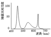
特に本実施の形態では、白色LED2e1として、青色LEDと緑および赤の波長領域に発光のピークを持つ蛍光体を組み合わせて色再現性を改善したLEDを採用している。図4に、本実施の形態で採用した白色LED2e1の発光スペクトル分布図を示す。図4に示した白色LEDでは、図3に示した従来の白色LEDの発光スペクトル分布図と比較し、緑および赤の波長領域に明確なピークを有するため、より広い範囲の色域を再現することが可能となり、特に図3に示した黄色蛍光体を用いた従来の白色LEDでは不利であった赤色の再現性においての改善効果が大きい。
<Configuration of light source unit>
As described above, in the present embodiment, as the white LED 2e1 of the
In particular, in the present embodiment, as the white LED 2e1, an LED having improved color reproducibility by combining a blue LED and a phosphor having emission peaks in the green and red wavelength regions is employed. FIG. 4 shows an emission spectrum distribution diagram of the white LED 2e1 employed in the present embodiment. The white LED shown in FIG. 4 has a clear peak in the green and red wavelength regions compared to the emission spectrum distribution diagram of the conventional white LED shown in FIG. 3, and thus reproduces a wider color gamut. In particular, the effect of improving red reproducibility, which was disadvantageous in the conventional white LED using the yellow phosphor shown in FIG. 3, is great.
<表示制御回路の構成>
図10は、液晶表示装置100に入力画像信号6を供給する表示機器から入力画像信号6および輝度調整信号71を入力して、液晶表示素子1に画像出力データを出力する(出力画像データ)と共に、バックライト2にLED駆動信号54を出力する制御回路基板4のブロック図である。さらに詳しくは、制御回路基板4は、図中破線で示した表示制御回路5とLED駆動回路7から構成され、前記制御回路基板4には前記入力画像信号6と前記輝度調整信号71が入力する。すなわち前記輝度調整信号71は、制御回路基板4内の配線を介してLED駆動回路7に入力する。ここで、前記輝度調整信号71は、上述したようにバックライト2の輝度を所望の値に調整するために、輝度に対応したデューティ比を持つPWM信号であり、そのPWM値の情報はLED駆動回路7から出力し、制御回路基板4内の配線を介して色度演算処理部51に入力する。
<Configuration of display control circuit>
FIG. 10 shows an
<白色LEDの特性>
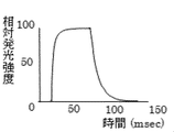
図5は、本実施の形態にて使用する白色LED2e1に、LED駆動信号54が印加された場合の赤色蛍光体による相対的な発光強度と時間の応答特性図である。青色LED自身、および青色LEDの光に対して応答性のよい緑色蛍光体が励起されて光が発せられる場合、LED駆動信号54に対する発光強度の応答性には、顕著な遅れは生じない。しかし、青色LEDの光に対して赤色蛍光体が励起されて光が発せられる場合、発光強度の時間的特性は図5に示したように、入力信号に対する遅れが生じる。この遅れは、赤色蛍光体として使用される蛍光体の材料特性に起因している。
<Characteristics of white LED>
FIG. 5 is a response characteristic diagram of relative light emission intensity and time by the red phosphor when the
<輝度調整動作>
図6は、白色LED2e1を光源として使用するバックライト2の輝度を、PWMにより調整する場合の白色LED2e1へのLED駆動信号54の波形図である。
<Brightness adjustment operation>
FIG. 6 is a waveform diagram of the
白色LEDを光源として使用したバックライト2の輝度を調整する場合、一般的には100Hzから1000Hzの範囲の一定の周波数を持つ矩形波の、出力オンとオフの比率(=デューティ比)を変えることにより、所望の輝度に調整するPWMを用いた輝度調整方法が採用される。本実施の形態でも当該PWMを用いた輝度調整を採用しており、図6に例示した波形は、周波数200Hz、デューティ比50%(=輝度50%)時のLED駆動信号54の波形図である。さらに図7は、図6に示したLED駆動信号54で、図4に示した白色LED2e1を連続点灯させた場合の、赤色蛍光体が励起されて発せられる光の強度と時間との応答特性図である。
When adjusting the luminance of the
デューティ比100%で白色LED2e1を点灯させた場合は、蛍光体が励起されて発光する際の応答性の違いの影響は生じず、液晶表示装置100としての設定された仕様通りの色度が得られる。しかし、白色LED2e1のPWM駆動による光源部2eの輝度調整を行った場合は、応答性の悪い蛍光体の発光色に関しては、LED駆動信号54の波形と、実際の発光強度の応答波形に違いが生じ、図5および図7に示したように、LED駆動信号54がオフ(Off)時にも、発光が残る特性が強い場合は、デューティ比100%時を基準に設定された色度に対して、赤色が相対的に強く表示され、バックライト2の白色色度のずれが生じてしまう。その白色色度ずれの結果、液晶表示装置100の色度ずれが生じる。
When the white LED 2e1 is turned on at a duty ratio of 100%, there is no influence of the difference in responsiveness when the phosphor is excited to emit light, and the chromaticity according to the set specification as the liquid
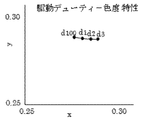
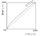
図8は、LED駆動信号54のデューティ比を変えて輝度調整を行った場合の、白色LEDの色度の変化を表した色度図である。図9は、LED駆動信号54に対応する入力デューティ比と、赤色蛍光体の相対発光強度として得られる実行デューティ比の関係を表す相関図である。
FIG. 8 is a chromaticity diagram showing a change in chromaticity of the white LED when luminance adjustment is performed by changing the duty ratio of the
図8は、図4に示した発光スペクトル分布特性と、図5に示した赤色蛍光体の応答特性を持つ白色LED2e1を光源とした液晶表示装置100において、LED駆動信号54のデューティ比を変えて輝度調整を行った場合の、白色LEDの色度の変化を表した色度図である。図8において、d100はデューティ比100%時の色度であり、さらにd100>d1>d2>d3へとデューティ比を減少させた場合(図9中の矢印方向)、デューティ比が小さくなるほど、当初の色度からのずれが大きくなる。
FIG. 8 shows a liquid
上記白色LEDの色度ずれ現象は、図9に示したように、0%から100%までの入力デューティ比で当該白色LED2e1を駆動した場合、実施に赤色蛍光体の相対発光強度として得られる実行デューティ比が、0%,100%の両端部を除く中央部で盛り上がっていることに起因している。この現象は、図5、図7に示したように、赤色蛍光体の応答特性がオン(On)応答に比べて、オフ応答が悪いことに起因している。なお、図9中に一点鎖線で示した直線が、白色LED2e1の赤色蛍光体の応答遅れが無い場合の理想的なLEDの場合の実行デューティ比である。(一対一のリニアな相関関係を表す。) As shown in FIG. 9, the white LED chromaticity shift phenomenon is obtained as the relative emission intensity of the red phosphor when the white LED 2e1 is driven at an input duty ratio of 0% to 100%. This is due to the fact that the duty ratio rises at the central portion excluding both end portions of 0% and 100%. As shown in FIGS. 5 and 7, this phenomenon is caused by the fact that the response characteristic of the red phosphor is poorer than the on (On) response. In addition, the straight line shown with the dashed-dotted line in FIG. 9 is the execution duty ratio in the case of an ideal LED when there is no response delay of the red phosphor of the white LED 2e1. (Represents a one-to-one linear correlation.)
図8に示したように、駆動デューティ比が100%から小さくなると色度が赤色方向にずれるため、そのずれ量に相当するデューティ比が駆動デューティ比に加わったことになる。図9中、実線が入力する駆動デューティ比と、赤色の実行デューティ比との関係を表す(ノンリニアな曲線)相関図であり、特定の駆動デューティ比時における前記一点鎖線と実線の差分が、何らかの補正が必要な値となる。 As shown in FIG. 8, when the drive duty ratio decreases from 100%, the chromaticity shifts in the red direction, so that the duty ratio corresponding to the shift amount is added to the drive duty ratio. FIG. 9 is a (nonlinear curve) correlation diagram showing the relationship between the drive duty ratio inputted by the solid line and the red duty ratio (nonlinear curve), and the difference between the one-dot chain line and the solid line at a specific drive duty ratio is The value needs to be corrected.
従って、液晶表示装置100の白色表示時において、白色LEDをPWM駆動して輝度調整を行った場合、駆動デューティ比に応じて、白色表示の色度変化が生じる。ここで白色表示時とは、液晶表示素子1の、RGB各画素の透過率を最大とした場合である。本実施の形態では、表示機器本体から入力する入力画像信号6がRGB各8ビットのデータ構成となっており、0〜255階調を取り得る。
Accordingly, when the brightness is adjusted by PWM driving the white LED during white display of the liquid
<白色色度補正の方法>
これら白色表示時(=RGB各色の階調が255階調の時)の色度変化の現象の対策として、本実施の形態においては、予め蛍光体が励起され発光する際の応答性を把握したうえで、液晶表示素子1の画素へ入力される本来の入力画像信号6に対し、補正データを加えて電圧を入力することで色度変化を抑える。
<White chromaticity correction method>
As a countermeasure against the phenomenon of chromaticity change at the time of white display (= when each RGB gradation is 255 gradations), in the present embodiment, the responsiveness when the phosphor is excited and emits light is grasped in advance. In addition, the chromaticity change is suppressed by adding correction data to the original
本実施の形態における例示では、白色表示時の上記色度の変化が、主に白色LEDの赤色蛍光体の応答遅れに起因しているので、RGBの3色から成る入力画像信号6の内、赤(Red)の画像信号にのみ補正を行う。
In the exemplification in the present embodiment, the change in chromaticity at the time of white display is mainly caused by the response delay of the red phosphor of the white LED. Therefore, among the
具体的には、まず第1ステップとして、白色表示時において、白色LEDをPWM駆動での各デューティ比に対する色度変化の内、赤色成分の誤差データを測定あるいはシミュレーションにより把握する。 Specifically, as a first step, during white display, error data of the red component is grasped by measurement or simulation in the chromaticity change with respect to each duty ratio when the white LED is PWM driven.
具体的には、上述の各デューティ比において、前記赤色成分の誤差データに対して、前記色度変化の要因となっている発光色(本実施の形態においては、赤色)の入力画像信号6の各階調に応じた補正データ(階調補正データ)を求める。
Specifically, at each of the above-described duty ratios, the
本実施の形態では、補正データを測定するデューティ比を10%刻みとした。従ってデューティ比0%(常に白色LEDが点灯しない状態)と100%(白色LEDが連続点灯状態)を除く、10〜90%まで9種類の補正データを測定する。具体的には、デューティ比を測定する値の固定して、液晶表示装置100に白色表示を表示し(RGBとも最大階調値すなわち255階調時)、赤の画像信号の階調値を最大階調値から減少させて行き、デューティ比100%時の色度値に最も近似するよう減少幅を測定し、補正データとして記録する。以後、同様にデューティ比を10%刻みで変えながら上記減少幅を測定、記録し、合計9種類の補正データを得る。 In the present embodiment, the duty ratio for measuring the correction data is set in increments of 10%. Accordingly, nine types of correction data are measured from 10% to 90% excluding the duty ratio of 0% (the white LED is not always lit) and 100% (the white LED is continuously lit). Specifically, the value for measuring the duty ratio is fixed and white display is displayed on the liquid crystal display device 100 (maximum gradation value for RGB, that is, 255 gradations), and the gradation value of the red image signal is maximized. Decreasing from the gradation value, the reduction width is measured so as to approximate the chromaticity value when the duty ratio is 100%, and recorded as correction data. Thereafter, similarly, the reduction width is measured and recorded while changing the duty ratio in increments of 10% to obtain a total of nine types of correction data.
同様に、白色表示時のRGBの各色の階調を一斉に1ビット減少させて254階調とし、上述の第1ステップを実施して、254階調表示時の10%〜90%のデューティ比にて白色LED駆動時の赤の補データを得る。以降、同様に253階調〜1階調まで繰り返して、9種類のデューティ比に対応した256の赤の階調補正データを得る(0階調すなわち全黒時は補正不要なので255個でも良いが補正データを0として保持しておく。)。 Similarly, the gradation of each color of RGB at the time of white display is reduced by 1 bit at a time to 254 gradations, and the first step described above is performed, and a duty ratio of 10% to 90% at the time of 254 gradations display. To obtain the complementary red data when the white LED is driven. Thereafter, 256 gradations to 1 gradation are similarly repeated, and 256 red gradation correction data corresponding to nine types of duty ratios are obtained. The correction data is held as 0).
次に第2ステップとして、上記9種類のデューティ比に対応して、入力画像信号の階調に応じた補正値を保持する9個の番号を持つデータテーブル10を準備し、デューティ比をテーブル番号と対応付けて256個の補正値を保持しておく。すなわち、特定のデューティ比を指定すれば、入力画像信号6の0〜255の階調値に応じた赤色画像信号の補正値を読み出すことが可能となる。
Next, as a second step, a data table 10 having nine numbers for holding correction values corresponding to the gradations of the input image signal corresponding to the nine types of duty ratios is prepared, and the duty ratio is set to the table number. The 256 correction values are stored in association with each other. That is, if a specific duty ratio is designated, it is possible to read out the correction value of the red image signal corresponding to the gradation value of 0 to 255 of the
図11に、上記データテーブル10の一例を図示する。同図に示したように、デューティ比10%〜90%毎に分かれて256個の階調値に対応した補正値が保存されている(20%、30%、70%、80%デューティ比は図示を省略した。)。すなわち、特定のデューティ比を指定すれば、入力画像信号6の0〜255の階調値に応じた赤色画像信号の階調補正データを読み出すことが可能となる。
FIG. 11 illustrates an example of the data table 10. As shown in the figure, correction values corresponding to 256 gradation values are stored for each duty ratio of 10% to 90% (20%, 30%, 70%, 80% duty ratio is (The illustration is omitted.) That is, if a specific duty ratio is specified, it is possible to read out the gradation correction data of the red image signal corresponding to the gradation values of 0 to 255 of the
次の第3ステップが実際に液晶表示素子1に画像表示を行うためのステップとなる。このステップでは、バックライト2の輝度調整値の情報、すなわちPWM信号に関する情報(デューティ比に関する情報)に応じ、画像入力に対する補正を行う。
The next third step is a step for actually displaying an image on the liquid
<表示制御回路の動作>
表示制御回路5は、表示機器からの入力画像信号6に対して、色度演算処理部51において、LED駆動回路7(輝度制御部)から出力されるPWM信号のデューティ比に関する情報に応じて、予め書き込まれた階調補正データに基づき、PWMで色度変化の生じる色に関し演算処理を行い、補正された画像信号を生成し、表示素子駆動部53へ映像データとして出力する。
<Operation of display control circuit>
The
具体的には、本実施の形態では、赤色蛍光体の応答遅れを補正しており、入力した赤色の入力画像信号6から、その階調値に応じて、前記デューティ比をパラメータとして上記データテーブル10に保持された階調補正データを読み出し、前記入力階調値から階調補正データ分を減算して表示素子駆動部53へ赤の映像データとして出力する。
Specifically, in the present embodiment, the response delay of the red phosphor is corrected, and the data table described above is used with the duty ratio as a parameter from the input red
次に、該映像データを受けた表示素子駆動部53は、当該赤の階調補正済みの画像出力データと他の補正しない青や緑の画像データや、他のタイミング信号等(非図示)を用いて液晶表示素子1を駆動する。
Next, the display
こうして蛍光体の励起、発光時の応答特性、PWM信号のデューティ比によらず、一定の色度の表示を得ることが出来る。 In this way, a display with a constant chromaticity can be obtained regardless of the excitation of the phosphor, the response characteristics during light emission, and the duty ratio of the PWM signal.
<作用>
上記階調補正された液晶表示素子への出力データにより、実際に表示される画像においては、PWMによる輝度調整で生じるバックライトの白色LED光源の色度変化が、当該色の画素の階調補正により相殺され、輝度によらず一定の色度を維持することが可能となる。
<Action>
In the image actually displayed by the output data to the liquid crystal display element subjected to the gradation correction, the chromaticity change of the white LED light source of the backlight generated by the luminance adjustment by PWM is the gradation correction of the pixel of the color. Therefore, a constant chromaticity can be maintained regardless of the luminance.
上記説明したとおり、本発明の液晶表示装置100によれば、青色LEDと、緑色および赤色の波長領域に発光のピークを持つ蛍光体を組み合わせた広色再現範囲対応の白色LEDを使用し、バックライト2の輝度をPWMにより調整した場合においても、LED蛍光体の応答特性に起因する色度変化を、画像入力データに対する階調補正を行うことにより、表示の明るさ設定によらず本来の製品仕様としての色度を維持することが出来る。
As described above, according to the liquid
なお、上述の実施の形態1においては、白色LED2e1は光源基板2e2上に複数配置されているとしたが、特に白色LEDは複数である必要はなく、光量が十分であれば、1個だけでもよい。 In the first embodiment described above, a plurality of white LEDs 2e1 are arranged on the light source substrate 2e2. However, the number of white LEDs does not have to be particularly plural, and if the amount of light is sufficient, only one LED can be used. Good.
<変形例>
上述の実施の形態1においては、図1に示したように導光板2cの側面2c3に光源部2eを配置した、エッジ入光タイプのバックライトについて例示したが、導光板2cを備えず、液晶表示素子1の裏面と対向するリヤフレーム2fの底面の概ね全面に光源を一定の間隔で配置した、いわゆる直下型バックライトに対しても、同様の効果を得ることができる。
<Modification>
In the above-described first embodiment, as illustrated in FIG. 1, an edge light incident type backlight in which the
実施の形態2.
上述の実施の形態1では、上記階調補正データは、白色LEDを駆動する信号のPWMの各デューティ比に対応して、定量化された数値データをデータテーブル化して、表示制御回路5に保持していたが、本実施の形態2では、図12に示したように、実施の形態1における構成に加えて、バックライト2内または近傍に色度センサー8をさらに設置し、該色度センサー8での色度測定値を色成分分析回路9で赤色成分を抽出し(赤色を通過させるフィルタ処理)、表示制御回路5へ赤色強度情報(赤色強度データ)をフィードバック信号として入力する。表示制御回路5内の色度演算処理部51にて、その赤色強度情報を取り込み、本来の色度仕様と比較し階調補正値を演算処理により求めることで、液晶表示素子1への出力を求める。
In the first embodiment, the gradation correction data is stored in the
その際、上述の実施の形態1にて説明したPWM情報は、上記演算時に数値演算の階調補正データの初期値を決めることに使用される。色度演算処理部51において、LED駆動回路7から入力したPWM情報に基づいて、数値演算時の階調補正データ初期値を決定し、さらに前記赤色強度情報に基づいて、所定の白色色度に合わせこんで行く。 At that time, the PWM information described in the first embodiment is used to determine an initial value of gradation correction data for numerical calculation during the calculation. In the chromaticity calculation processing unit 51, the gradation correction data initial value at the time of numerical calculation is determined based on the PWM information input from the LED drive circuit 7, and further, the predetermined white chromaticity is determined based on the red intensity information. Go together.
具体的には、色度演算処理部51にて赤色強度情報を、表示素子駆動部53から出力する画像出力データの赤の階調補正にフィードバックする。すなわちPWM信号のデューティ比および入力階調値をパラメータとした上記データテーブル10のメモリ値を階調補正データの初期値とし、前記赤色強度情報と仕様により求められる所定の赤色強度とを比較して、前記赤色強度情報が大きい場合は前記初期の階調補正データ値を1階調増加させる処理(=赤色表示階調値を1減ずる)を行い、逆に前記赤色強度情報が小さい場合は前記初期の階調補正データ値を1階調減ずる処理(=赤色表示階調値を1増やす)を行う。この補正動作(補正データの増減動作)を繰り返し行うことにより前記赤色強度情報が前記所定の赤色強度と合致する。
Specifically, the chromaticity calculation processing unit 51 feeds back red intensity information to the red tone correction of the image output data output from the display
このように、バックライト2内または近傍に色度センサー8および色成分分析回路9を具備し、色度演算処理部51において、PWM情報と赤色強度情報を演算処理に用いることにより、液晶表示装置100の白色色度を所定の値に素早く、またバラつきが少なく、正確に合わせこむことができる。
As described above, the chromaticity sensor 8 and the color component analysis circuit 9 are provided in or near the
なお、上述の実施の形態2では、バックライト2の赤色成分の強度を測定するために、色度センサー8および色成分分析回路9を用いたが、赤色の波長成分のみを通過させる光学フィルタ(赤色フィルタ)と、その波長に反応するフォトレジスタや、受光センサ(光学センサに該当する)の組み合わせでも同様の効果を奏することができる。
In the second embodiment described above, the chromaticity sensor 8 and the color component analysis circuit 9 are used to measure the intensity of the red component of the
実施の形態3.
さらに上述の実施の形態1における構成に加えて、液晶表示素子1の前面に、外部より画面に対する位置信号入力を行うためのタッチパネルおよびタッチパネルを保護するための概ね透明の保護部材(共に非図示)、後面には制御回路基板4を保護するためのカバー(非図示)を備えてもよい。
Further, in addition to the configuration in the first embodiment described above, a touch panel for inputting a position signal to the screen from the outside and a generally transparent protective member for protecting the touch panel on the front surface of the liquid crystal display element 1 (both not shown). The rear surface may be provided with a cover (not shown) for protecting the
<タッチパネル>
タッチパネル(非図示)は、透明な基板上に形成された透明電極による回路により外部(使用者)から入力された位置座標に関する情報を電気信号に変換し、端部に接続された出力配線部を介して最終製品の制御回路へ伝達する。出力配線部としては、薄さと柔軟性による接続の自由度から、フィルム上の基材に配線を形成したFPCが用いられるが、同等の機能、特性を有するものであれば、異なる材料、構造から成るものでもよい。
<Touch panel>
A touch panel (not shown) converts information related to position coordinates input from the outside (user) into an electrical signal by a circuit using a transparent electrode formed on a transparent substrate, and outputs an output wiring unit connected to an end. To the control circuit of the final product. As the output wiring part, FPC in which wiring is formed on the base material on the film is used from the degree of freedom of connection due to thinness and flexibility. However, as long as it has the same function and characteristics, different materials and structures can be used. It may consist of.
また、タッチパネルは、入力面側からの加圧や接触による損傷、変形、磨耗、汚れ等を防止するために、ガラスあるいはプラスチック等の透明材料からなる保護部材(非図示)を、前面側に備えてもよく、保護部材の表面あるいは裏面の周辺部へは、遮光あるいは意匠上の目的により、印刷を付加することもできる。 In addition, the touch panel is provided with a protective member (not shown) made of a transparent material such as glass or plastic on the front side in order to prevent damage, deformation, wear, dirt, etc. due to pressure or contact from the input side. In addition, printing may be added to the periphery of the front surface or the back surface of the protective member for light shielding or design purposes.
上記実施の形態1ないし3に係る説明では、白色LEDに使用された応答の悪い蛍光体により、設定された色度仕様から変化する成分として赤色と仮定して説明したが、応答の悪い蛍光体は、赤色に限定する必要はなく、他の色を発する蛍光体であってもよく、さらには、一色に限定する必要はなく複数の色に対応した階調補正データを準備可能であれば、複数の色に蛍光体でも対応可能である。 In the description of the first to third embodiments described above, it is assumed that red is used as the component that changes from the set chromaticity specification due to the poor response phosphor used in the white LED, but the poor response phosphor. Is not limited to red, and may be a phosphor that emits other colors. Further, if it is possible to prepare gradation correction data corresponding to a plurality of colors without being limited to one color, A plurality of colors can also be handled by a phosphor.
1 液晶表示素子
11 カラーフィルタ基板
12 TFT基板
13 ドライバIC
2 バックライト
2a ミドルフレーム
2b 光学シート
2c 導光板
2c1 出射面
2c2 反出射面
2d 反射シート
2e 光源部
2e1 白色LED
2e2 光源基板
2f リヤフレーム
3 フロントフレーム
3a 表示用開口部
4 制御回路基板
5 表示制御回路
51 色度演算処理部
53 表示素子駆動部
54 LED駆動信号
6 入力画像信号
7 LED駆動回路
8 色度センサー
9 色度分析回路
10 データテーブル
71 輝度調整信号
100 液晶表示装置
DESCRIPTION OF
2 Backlight 2a
2e2
Claims (3)
前記白色発光ダイオードへの出力をパルス幅変調信号を用いて前記バックライトの輝度を調整する発光ダイオード制御回路をさらに備え、
前記表示制御回路は、前記パルス幅変調信号のデューティ比に応じた色度変化に対する階調補正データが予め準備されており、
前記液晶表示装置へ入力する入力画像データに対し、該入力画像データと前記デューティ比とに応じて前記色度変化を補正するよう前記階調補正データを割り当て、
該階調補正データと前記入力画像データとにより算出した出力画像データを前記画像信号として前記液晶表示素子に出力することを特徴とする液晶表示装置。 A liquid crystal display element comprising a color filter substrate and a TFT substrate, a display control circuit for generating an image signal for controlling the display of the liquid crystal display element, and at least one white light emitting diode disposed on the back surface of the liquid crystal display element And a backlight that emits planar light from the exit surface, and a liquid crystal display device comprising:
A light emitting diode control circuit for adjusting the brightness of the backlight using a pulse width modulation signal to the white light emitting diode;
In the display control circuit, gradation correction data for chromaticity change according to the duty ratio of the pulse width modulation signal is prepared in advance,
Assigning the gradation correction data to the input image data to be input to the liquid crystal display device so as to correct the chromaticity change according to the input image data and the duty ratio;
A liquid crystal display device, wherein output image data calculated from the gradation correction data and the input image data is output to the liquid crystal display element as the image signal.
該赤色強度データにより、前記階調補正データを増減することを特徴とする請求項1または2に記載の液晶表示装置。 A red intensity data is generated by combining an optical sensor that measures the intensity of light emitted from the backlight and a filter that extracts red,
3. The liquid crystal display device according to claim 1, wherein the gradation correction data is increased or decreased according to the red intensity data.
Priority Applications (3)
| Application Number | Priority Date | Filing Date | Title |
|---|---|---|---|
| JP2015115820A JP6524807B2 (en) | 2015-06-08 | 2015-06-08 | Liquid crystal display |
| US15/171,424 US10078985B2 (en) | 2015-06-08 | 2016-06-02 | Liquid crystal display |
| CN201610397775.6A CN106249473B (en) | 2015-06-08 | 2016-06-07 | Liquid crystal display device |
Applications Claiming Priority (1)
| Application Number | Priority Date | Filing Date | Title |
|---|---|---|---|
| JP2015115820A JP6524807B2 (en) | 2015-06-08 | 2015-06-08 | Liquid crystal display |
Publications (3)
| Publication Number | Publication Date |
|---|---|
| JP2017003699A true JP2017003699A (en) | 2017-01-05 |
| JP2017003699A5 JP2017003699A5 (en) | 2018-06-21 |
| JP6524807B2 JP6524807B2 (en) | 2019-06-05 |
Family
ID=57450988
Family Applications (1)
| Application Number | Title | Priority Date | Filing Date |
|---|---|---|---|
| JP2015115820A Active JP6524807B2 (en) | 2015-06-08 | 2015-06-08 | Liquid crystal display |
Country Status (3)
| Country | Link |
|---|---|
| US (1) | US10078985B2 (en) |
| JP (1) | JP6524807B2 (en) |
| CN (1) | CN106249473B (en) |
Cited By (5)
| Publication number | Priority date | Publication date | Assignee | Title |
|---|---|---|---|---|
| JP2018145603A (en) * | 2017-03-01 | 2018-09-20 | 株式会社荏原製作所 | A feed water equipment and a monitoring system |
| WO2019189028A1 (en) * | 2018-03-29 | 2019-10-03 | パナソニックIpマネジメント株式会社 | Display control device and display control method |
| US10545374B2 (en) | 2018-02-20 | 2020-01-28 | Qingdao Hisense Electronics Co., Ltd. | Light source control apparatus, light source control method and display device |
| US11837181B2 (en) | 2021-02-26 | 2023-12-05 | Nichia Corporation | Color balancing in display of multiple images |
| WO2024038997A1 (en) * | 2022-08-17 | 2024-02-22 | 삼성전자주식회사 | Display device comprising led driving circuit, and driving method |
Families Citing this family (11)
| Publication number | Priority date | Publication date | Assignee | Title |
|---|---|---|---|---|
| US10600213B2 (en) * | 2016-02-27 | 2020-03-24 | Focal Sharp, Inc. | Method and apparatus for color-preserving spectrum reshape |
| US10398002B2 (en) | 2017-05-05 | 2019-08-27 | Wuhan China Star Optoelectronics Technology Co., Ltd | Backlight module, LCD and backlight module driving control method |
| CN106935210A (en) * | 2017-05-05 | 2017-07-07 | 武汉华星光电技术有限公司 | Backlight module, liquid crystal display and backlight module drive control method |
| CN106940993B (en) * | 2017-05-23 | 2019-02-05 | 京东方科技集团股份有限公司 | A kind of display bearing calibration and system |
| JP6443867B1 (en) * | 2017-06-15 | 2018-12-26 | キヤノン株式会社 | Light emitting device, display device, and control method |
| KR102470567B1 (en) * | 2017-07-10 | 2022-11-24 | 엘지디스플레이 주식회사 | Display Device Having Optical Sensor |
| CN109285508A (en) * | 2018-11-27 | 2019-01-29 | 合肥惠科金扬科技有限公司 | A kind of driving method of display device, drive system and display device |
| TWI721375B (en) * | 2019-02-22 | 2021-03-11 | 友達光電股份有限公司 | Timing controller, display device and screen displaying method |
| CN110111691B (en) * | 2019-04-08 | 2021-03-30 | 苏州佳世达电通有限公司 | Display device |
| JP7322555B2 (en) * | 2019-07-05 | 2023-08-08 | セイコーエプソン株式会社 | Electro-optical devices, electronic devices and moving bodies |
| CN114063349B (en) * | 2021-09-28 | 2023-09-08 | 信阳中部半导体技术有限公司 | Cell-phone backlight unit based on heat transfer independently adjusts accuse temperature |
Citations (7)
| Publication number | Priority date | Publication date | Assignee | Title |
|---|---|---|---|---|
| JP2008083439A (en) * | 2006-09-28 | 2008-04-10 | Sharp Corp | Liquid crystal display device and method for adjusting white balance |
| JP2009086664A (en) * | 2007-09-27 | 2009-04-23 | Toppoly Optoelectronics Corp | Display device with ambient light sensing |
| JP2010039047A (en) * | 2008-08-01 | 2010-02-18 | Seiko Epson Corp | Projector, and control method and control program of projector |
| JP2010128040A (en) * | 2008-11-26 | 2010-06-10 | Panasonic Corp | Display device |
| JP2013186207A (en) * | 2012-03-06 | 2013-09-19 | Sharp Corp | Liquid crystal display device |
| US20140035960A1 (en) * | 2012-07-31 | 2014-02-06 | Apple Inc. | Backlight dimming control for a display utilizing quantum dots |
| JP2014170641A (en) * | 2013-03-01 | 2014-09-18 | Sharp Corp | Lighting device and display device provided with the same |
Family Cites Families (12)
| Publication number | Priority date | Publication date | Assignee | Title |
|---|---|---|---|---|
| JP2001272938A (en) | 2000-03-28 | 2001-10-05 | Sharp Corp | Color tone adjusting circuit and back light module and light emitting diode display device provided with the same circuit |
| KR100757785B1 (en) * | 2001-07-12 | 2007-09-11 | 삼성전자주식회사 | Method for illuminating light of liquid crystal display device and liquid crystal display device using the same |
| JP4156919B2 (en) | 2002-12-18 | 2008-09-24 | 三菱電機株式会社 | Planar light source device, liquid crystal display device, and display device |
| JP2004311635A (en) | 2003-04-04 | 2004-11-04 | Olympus Corp | Driving device, lighting device using the same, and indicating device using the lighting device |
| JP4438722B2 (en) | 2004-11-19 | 2010-03-24 | ソニー株式会社 | Backlight driving device, backlight driving method, and liquid crystal display device |
| KR101550347B1 (en) | 2007-12-04 | 2015-09-08 | 삼성디스플레이 주식회사 | Light assembly liquid crystal display and method of driving the light assembly |
| JP2010078802A (en) * | 2008-09-25 | 2010-04-08 | Sony Corp | Liquid crystal display |
| TWI406589B (en) | 2008-10-28 | 2013-08-21 | Ind Tech Res Inst | Control circuit and method for backlight sources, and image display apparatus and lighting apparatus using the same |
| JP5367883B2 (en) * | 2011-08-11 | 2013-12-11 | シャープ株式会社 | Illumination device and display device including the same |
| US20140340431A1 (en) * | 2011-11-30 | 2014-11-20 | SHARP KABUSHIKI KAISHA a corporation | Control unit, display device including control unit, and control method |
| JP2014227496A (en) | 2013-05-23 | 2014-12-08 | 三菱化学株式会社 | Phosphor, phosphor-containing composition and light-emitting device using the phosphor, and image display device and illuminating device using the light-emitting device |
| CN104503142A (en) * | 2015-01-26 | 2015-04-08 | 友达光电股份有限公司 | Liquid crystal display device, scanning method and mobile terminal capable of realizing color scanning |
-
2015
- 2015-06-08 JP JP2015115820A patent/JP6524807B2/en active Active
-
2016
- 2016-06-02 US US15/171,424 patent/US10078985B2/en active Active
- 2016-06-07 CN CN201610397775.6A patent/CN106249473B/en active Active
Patent Citations (7)
| Publication number | Priority date | Publication date | Assignee | Title |
|---|---|---|---|---|
| JP2008083439A (en) * | 2006-09-28 | 2008-04-10 | Sharp Corp | Liquid crystal display device and method for adjusting white balance |
| JP2009086664A (en) * | 2007-09-27 | 2009-04-23 | Toppoly Optoelectronics Corp | Display device with ambient light sensing |
| JP2010039047A (en) * | 2008-08-01 | 2010-02-18 | Seiko Epson Corp | Projector, and control method and control program of projector |
| JP2010128040A (en) * | 2008-11-26 | 2010-06-10 | Panasonic Corp | Display device |
| JP2013186207A (en) * | 2012-03-06 | 2013-09-19 | Sharp Corp | Liquid crystal display device |
| US20140035960A1 (en) * | 2012-07-31 | 2014-02-06 | Apple Inc. | Backlight dimming control for a display utilizing quantum dots |
| JP2014170641A (en) * | 2013-03-01 | 2014-09-18 | Sharp Corp | Lighting device and display device provided with the same |
Cited By (5)
| Publication number | Priority date | Publication date | Assignee | Title |
|---|---|---|---|---|
| JP2018145603A (en) * | 2017-03-01 | 2018-09-20 | 株式会社荏原製作所 | A feed water equipment and a monitoring system |
| US10545374B2 (en) | 2018-02-20 | 2020-01-28 | Qingdao Hisense Electronics Co., Ltd. | Light source control apparatus, light source control method and display device |
| WO2019189028A1 (en) * | 2018-03-29 | 2019-10-03 | パナソニックIpマネジメント株式会社 | Display control device and display control method |
| US11837181B2 (en) | 2021-02-26 | 2023-12-05 | Nichia Corporation | Color balancing in display of multiple images |
| WO2024038997A1 (en) * | 2022-08-17 | 2024-02-22 | 삼성전자주식회사 | Display device comprising led driving circuit, and driving method |
Also Published As
| Publication number | Publication date |
|---|---|
| JP6524807B2 (en) | 2019-06-05 |
| CN106249473A (en) | 2016-12-21 |
| US10078985B2 (en) | 2018-09-18 |
| CN106249473B (en) | 2019-06-14 |
| US20160358557A1 (en) | 2016-12-08 |
Similar Documents
| Publication | Publication Date | Title |
|---|---|---|
| JP6524807B2 (en) | Liquid crystal display | |
| WO2010016440A1 (en) | Backlight and display device using the same | |
| JP4264560B2 (en) | Backlight device, backlight control method, and liquid crystal display device | |
| US9322976B2 (en) | Lighting device, display device and television device | |
| EP1750248A2 (en) | Backlight unit, display apparatus comprising the same and control method thereof | |
| JP5600433B2 (en) | Display device with backlight | |
| RU2467366C1 (en) | Liquid crystal display device | |
| KR20060000544A (en) | Back light for display device, light source for display device, and light emitting diode using therefor | |
| US9135869B2 (en) | Display signal generator, display device, and method of image display | |
| KR20070044885A (en) | Apparatus for driving of back light, back light and liquid crystal display device having the same and method of the driving | |
| KR101015299B1 (en) | Liquid crystal display device having good image quality | |
| JP2006164935A (en) | Light generator and display having same | |
| JP2006267780A (en) | Liquid crystal display apparatus | |
| KR20110105298A (en) | Pwm signal generating circuit and method for dc-dc converter using diming signal and led driving circuit for back light having the same | |
| US20150304614A1 (en) | Display device and television device | |
| JPH08211361A (en) | Transmission type display device | |
| JP2007200888A (en) | Backlight assembly and liquid crystal display device having this | |
| US20180286297A1 (en) | Display Device With Color And Luminance Characterization And Compensation Methods | |
| KR20160003971A (en) | Display apparatus | |
| JP2013504089A (en) | Backlight unit, display device, and backlight unit control method | |
| JP2010517071A (en) | Color-controlled backlight display | |
| KR20050002566A (en) | Backlight for liquid crystal display device | |
| WO2010064568A1 (en) | Image display device and surface light source device | |
| US9286835B2 (en) | Driving circuit and driving method for light emitting diode and display apparatus using the same | |
| US10989958B2 (en) | Display device comprising a control substrate configured to control drive of display pixels |
Legal Events
| Date | Code | Title | Description |
|---|---|---|---|
| A521 | Request for written amendment filed |
Free format text: JAPANESE INTERMEDIATE CODE: A523 Effective date: 20180509 |
|
| A621 | Written request for application examination |
Free format text: JAPANESE INTERMEDIATE CODE: A621 Effective date: 20180509 |
|
| A977 | Report on retrieval |
Free format text: JAPANESE INTERMEDIATE CODE: A971007 Effective date: 20190116 |
|
| A131 | Notification of reasons for refusal |
Free format text: JAPANESE INTERMEDIATE CODE: A131 Effective date: 20190122 |
|
| A521 | Request for written amendment filed |
Free format text: JAPANESE INTERMEDIATE CODE: A523 Effective date: 20190315 |
|
| TRDD | Decision of grant or rejection written | ||
| A01 | Written decision to grant a patent or to grant a registration (utility model) |
Free format text: JAPANESE INTERMEDIATE CODE: A01 Effective date: 20190409 |
|
| A61 | First payment of annual fees (during grant procedure) |
Free format text: JAPANESE INTERMEDIATE CODE: A61 Effective date: 20190422 |
|
| R151 | Written notification of patent or utility model registration |
Ref document number: 6524807 Country of ref document: JP Free format text: JAPANESE INTERMEDIATE CODE: R151 |
|
| R250 | Receipt of annual fees |
Free format text: JAPANESE INTERMEDIATE CODE: R250 |
|
| R250 | Receipt of annual fees |
Free format text: JAPANESE INTERMEDIATE CODE: R250 |