JP2016537726A - Vector processing engine with merging circuit between execution unit and vector data memory and associated method - Google Patents
Vector processing engine with merging circuit between execution unit and vector data memory and associated method Download PDFInfo
- Publication number
- JP2016537726A JP2016537726A JP2016531030A JP2016531030A JP2016537726A JP 2016537726 A JP2016537726 A JP 2016537726A JP 2016531030 A JP2016531030 A JP 2016531030A JP 2016531030 A JP2016531030 A JP 2016531030A JP 2016537726 A JP2016537726 A JP 2016537726A
- Authority
- JP
- Japan
- Prior art keywords
- vector data
- data sample
- vector
- input
- sample set
- Prior art date
- Legal status (The legal status is an assumption and is not a legal conclusion. Google has not performed a legal analysis and makes no representation as to the accuracy of the status listed.)
- Granted
Links
Images


Classifications
-
- G—PHYSICS
- G06—COMPUTING OR CALCULATING; COUNTING
- G06F—ELECTRIC DIGITAL DATA PROCESSING
- G06F9/00—Arrangements for program control, e.g. control units
- G06F9/06—Arrangements for program control, e.g. control units using stored programs, i.e. using an internal store of processing equipment to receive or retain programs
- G06F9/30—Arrangements for executing machine instructions, e.g. instruction decode
- G06F9/30003—Arrangements for executing specific machine instructions
- G06F9/30007—Arrangements for executing specific machine instructions to perform operations on data operands
- G06F9/30036—Instructions to perform operations on packed data, e.g. vector, tile or matrix operations
-
- G—PHYSICS
- G06—COMPUTING OR CALCULATING; COUNTING
- G06F—ELECTRIC DIGITAL DATA PROCESSING
- G06F15/00—Digital computers in general; Data processing equipment in general
- G06F15/76—Architectures of general purpose stored program computers
- G06F15/80—Architectures of general purpose stored program computers comprising an array of processing units with common control, e.g. single instruction multiple data processors
- G06F15/8053—Vector processors
-
- G—PHYSICS
- G06—COMPUTING OR CALCULATING; COUNTING
- G06F—ELECTRIC DIGITAL DATA PROCESSING
- G06F9/00—Arrangements for program control, e.g. control units
- G06F9/06—Arrangements for program control, e.g. control units using stored programs, i.e. using an internal store of processing equipment to receive or retain programs
- G06F9/30—Arrangements for executing machine instructions, e.g. instruction decode
- G06F9/30003—Arrangements for executing specific machine instructions
- G06F9/30007—Arrangements for executing specific machine instructions to perform operations on data operands
- G06F9/30021—Compare instructions, e.g. Greater-Than, Equal-To, MINMAX
-
- G—PHYSICS
- G06—COMPUTING OR CALCULATING; COUNTING
- G06F—ELECTRIC DIGITAL DATA PROCESSING
- G06F9/00—Arrangements for program control, e.g. control units
- G06F9/06—Arrangements for program control, e.g. control units using stored programs, i.e. using an internal store of processing equipment to receive or retain programs
- G06F9/30—Arrangements for executing machine instructions, e.g. instruction decode
- G06F9/30003—Arrangements for executing specific machine instructions
- G06F9/30007—Arrangements for executing specific machine instructions to perform operations on data operands
- G06F9/30032—Movement instructions, e.g. MOVE, SHIFT, ROTATE, SHUFFLE
-
- G—PHYSICS
- G06—COMPUTING OR CALCULATING; COUNTING
- G06F—ELECTRIC DIGITAL DATA PROCESSING
- G06F9/00—Arrangements for program control, e.g. control units
- G06F9/06—Arrangements for program control, e.g. control units using stored programs, i.e. using an internal store of processing equipment to receive or retain programs
- G06F9/30—Arrangements for executing machine instructions, e.g. instruction decode
- G06F9/38—Concurrent instruction execution, e.g. pipeline or look ahead
- G06F9/3885—Concurrent instruction execution, e.g. pipeline or look ahead using a plurality of independent parallel functional units
- G06F9/3887—Concurrent instruction execution, e.g. pipeline or look ahead using a plurality of independent parallel functional units controlled by a single instruction for multiple data lanes [SIMD]
-
- G—PHYSICS
- G06—COMPUTING OR CALCULATING; COUNTING
- G06F—ELECTRIC DIGITAL DATA PROCESSING
- G06F9/00—Arrangements for program control, e.g. control units
- G06F9/06—Arrangements for program control, e.g. control units using stored programs, i.e. using an internal store of processing equipment to receive or retain programs
- G06F9/30—Arrangements for executing machine instructions, e.g. instruction decode
- G06F9/38—Concurrent instruction execution, e.g. pipeline or look ahead
- G06F9/3885—Concurrent instruction execution, e.g. pipeline or look ahead using a plurality of independent parallel functional units
- G06F9/3888—Concurrent instruction execution, e.g. pipeline or look ahead using a plurality of independent parallel functional units controlled by a single instruction for multiple threads [SIMT] in parallel
-
- G—PHYSICS
- G06—COMPUTING OR CALCULATING; COUNTING
- G06F—ELECTRIC DIGITAL DATA PROCESSING
- G06F9/00—Arrangements for program control, e.g. control units
- G06F9/06—Arrangements for program control, e.g. control units using stored programs, i.e. using an internal store of processing equipment to receive or retain programs
- G06F9/30—Arrangements for executing machine instructions, e.g. instruction decode
- G06F9/38—Concurrent instruction execution, e.g. pipeline or look ahead
- G06F9/3885—Concurrent instruction execution, e.g. pipeline or look ahead using a plurality of independent parallel functional units
- G06F9/3893—Concurrent instruction execution, e.g. pipeline or look ahead using a plurality of independent parallel functional units controlled in tandem, e.g. multiplier-accumulator
- G06F9/3895—Concurrent instruction execution, e.g. pipeline or look ahead using a plurality of independent parallel functional units controlled in tandem, e.g. multiplier-accumulator for complex operations, e.g. multidimensional or interleaved address generators, macros
- G06F9/3897—Concurrent instruction execution, e.g. pipeline or look ahead using a plurality of independent parallel functional units controlled in tandem, e.g. multiplier-accumulator for complex operations, e.g. multidimensional or interleaved address generators, macros with adaptable data path
Landscapes
- Engineering & Computer Science (AREA)
- Theoretical Computer Science (AREA)
- Software Systems (AREA)
- Physics & Mathematics (AREA)
- General Engineering & Computer Science (AREA)
- General Physics & Mathematics (AREA)
- Computer Hardware Design (AREA)
- Mathematical Physics (AREA)
- Computing Systems (AREA)
- Advance Control (AREA)
- Executing Machine-Instructions (AREA)
- Complex Calculations (AREA)
Abstract
ベクトルデータメモリに記憶される出力ベクトルデータのインフライトマージングを提供するために、実行ユニットとベクトルデータメモリとの間のデータフローパスにおいてマージング回路を利用するベクトル処理エンジン(VPE)が開示される。関連するベクトル処理の命令、システム、および方法も開示される。マージング回路は、VPE内の実行ユニットとベクトルデータメモリとの間のデータフローパス内に設けられる。マージング回路は、出力ベクトルデータサンプルセットが記憶されるために実行ユニットからベクトルデータメモリに出力データフローパスを介して供給されている間のインフライトのベクトル処理動作を実行する結果として、実行ユニットからの出力ベクトルデータサンプルセットをマージするように構成される。マージされた出力ベクトルデータサンプルセットは、実行ユニット内で実行されるべき次のベクトル処理動作を遅延させる可能性がある、さらなる後処理ステップを必要とせずに、ベクトルデータメモリにマージされた形式で記憶される。【選択図】図31A vector processing engine (VPE) is disclosed that utilizes a merging circuit in the data flow path between the execution unit and the vector data memory to provide in-flight merging of output vector data stored in the vector data memory. Related vector processing instructions, systems, and methods are also disclosed. The merging circuit is provided in the data flow path between the execution unit in the VPE and the vector data memory. The merging circuit performs an in-flight vector processing operation while the output vector data sample set is being supplied from the execution unit to the vector data memory via the output data flow path to be stored. It is configured to merge the output vector data sample sets. The merged output vector data sample set is in a form merged into vector data memory without the need for further post-processing steps that may delay the next vector processing operation to be performed within the execution unit. Remembered. [Selection] Figure 31
Description
[0001]本出願は、2013年3月13日に出願され、参照によりその全体が本明細書に組み込まれている、「VECTOR PROCESSING ENGINES HAVING PROGRAMMABLE DATA PATH CONFIGURATIONS FOR PROVIDING MULTI−MODE VECTOR PROCESSING, AND RELATED VECTOR PROCESSORS, SYSTEMS, AND METHODS」、123249と題する、米国特許出願第13/798,641号に関連する。 [0001] This application was filed on March 13, 2013 and is hereby incorporated by reference in its entirety, "VECTOR PROCESSING ENGINES HAVING PROGRAMMABLE DATA PATH CONFIGURATIONS FOR PROVIDING MULTITED ED Related to US patent application Ser. No. 13 / 798,641, entitled “VECTOR PROCESSORS, SYSTEMS, AND METHODS”, 123249.
[0002]本出願は、2013年3月13日に出願され、参照によりその全体が本明細書に組み込まれている、「VECTOR PROCESSING CARRY−SAVE ACCUMULATORS EMPLOYING REDUNDANT CARRY−SAVE FORMAT TO REDUCE CARRY PROPAGATION, AND RELATED VECTOR PROCESSORS, SYSTEMS, AND METHODS」、123248と題する、米国特許出願第13/798,618号に関連する。 [0002] This application was filed on March 13, 2013, and is incorporated herein by reference in its entirety, "VECTOR PROCESSING CARRY-SAVE ACCUMULATORS EMPLOYING REDUNDANT CARRY-SAVE FORMAT TO REDUPRAND CARRY. Related to US patent application Ser. No. 13 / 798,618, entitled RELATED VECTOR PROCESSORS, SYSTEMS, AND METHODS, 123248.
[0003]本出願は、2013年11月15日に出願され、参照によりその全体が本明細書に組み込まれている、「VECTOR PROCESSING ENGINES (VPEs) EMPLOYING A TAPPED−DELAY LINE(S) FOR PROVIDING PRECISION FILTER VECTOR PROCESSING OPERATIONS WITH REDUCED SAMPLE RE−FETCHING AND POWER CONSUMPTION, AND RELATED VECTOR PROCESSOR SYSTEMS AND METHODS」、124362と題する、米国特許出願第14/082,075号にも関連する。 [0003] This application is filed on Nov. 15, 2013, which is incorporated herein by reference in its entirety, "VECTOR PROCESSING ENGINES (VPEs) EMPLOYING A TAPED-DELAY LINE (S) FOR PROVIDING PRECISION" FILTER VECTOR PROCESSING OPERATIONS WITH REDUCED SAMPLE RE-FETCHING AND POWER CONSUMPTION, AND RELATED VECTOR PROCESSOR SYSTEMS AND METHODS "
[0004]本出願は、2013年11月15日に出願され、参照によりその全体が本明細書に組み込まれている、「VECTOR PROCESSING ENGINES (VPEs) EMPLOYING TAPPED−DELAY LINE(S) FOR PROVIDING PRECISION CORRELATION/COVARIANCE VECTOR PROCESSING OPERATIONS WITH REDUCED SAMPLE RE−FETCHING AND POWER CONSUMPTION, AND RELATED VECTOR PROCESSOR SYSTEMS AND METHODS」、124364と題する、米国特許出願第14/082,079号にも関連する。
[0004] This application is filed on November 15, 2013, and is incorporated herein by reference in its entirety, "VECTOR PROCESSING ENGINES (VPEs) EMPLOYING TAPPED-DELAY LINE (S) FOR PROVIDING PRECISION CORRELATION. / COVARIANCE VECTOR PROCESSING OPERATIONS WITH REDUCED SAMPLE RE-FETCHING AND POWER CONSUMPTION, AND RELATED
[0005]本出願は、2013年11月15日に出願され、参照によりその全体が本明細書に組み込まれている、「VECTOR PROCESSING ENGINES (VPEs) EMPLOYING FORMAT CONVERSION CIRCUITRY IN DATA FLOW PATHS BETWEEN VECTOR DATA MEMORY AND EXECUTION UNITS TO PROVIDE IN−FLIGHT FORMAT−CONVERTING OF INPUT VECTOR DATA TO EXECUTION UNITS FOR VECTOR PROCESSING OPERATIONS, AND RELATED VECTOR PROCESSOR SYSTEMS AND METHODS」、124365と題する、米国特許出願第14/082,088号にも関連する。 [0005] This application is filed on November 15, 2013 and is incorporated herein by reference in its entirety, "VECTOR PROCESSING ENGINES (VPEs) EMPLOYING FORMAT CONVERSION CIRCUITRY DATA FLOWOR BETWEME BETWEET AND EXECUTION UNITS TO PROVIDE IN-FLIGHT FORMAT-CONVERTING OF INPUT VECTOR DATA TO EXECUTION UNITS FOR VECTOR PROCESSING OPERATIONS, AND RELATIVES "Entitled 124365 also relates to U.S. Patent Application No. 14 / 082,088.
[0006]本出願は、2013年11月15日に出願され、参照によりその全体が本明細書に組み込まれている、「VECTOR PROCESSING ENGINES (VPEs) EMPLOYING REORDERING CIRCUITRY IN DATA FLOW PATHS BETWEEN EXECUTION UNITS AND VECTOR DATA MEMORY TO PROVIDE IN−FLIGHT REORDERING OF OUTPUT VECTOR DATA STORED TO VECTOR DATA MEMORY, AND RELATED VECTOR PROCESSOR SYSTEMS AND METHODS」、124450と題する、米国特許出願第14/082,081号にも関連する。 [0006] This application was filed on November 15, 2013, and is hereby incorporated by reference in its entirety, "VECTOR PROCESSING ENGINES (VPEs) EMPLOYING REORDERING BETWEEN EXTECUENT EXTECUENT EXECT DATA MEMORY TO PROVIDE IN-FLIGHT REORDERING OF OUTPUT VECTOR DATA STORED TO VECTOR DATA MEMORY, AND RELATED VECTOR PROCESSOR SYSTEMS AND METHODS, US Patent No. 1244500 To.
[0007]本出願は、2013年11月15日に出願され、参照によりその全体が本明細書に組み込まれている、「VECTOR PROCESSING ENGINES (VPEs) EMPLOYING DESPREADING CIRCUITRY IN DATA FLOW PATHS BETWEEN EXECUTION UNITS AND VECTOR DATA MEMORY TO PROVIDE IN−FLIGHT DESPREADING OF SPREAD−SPECTRUM SEQUENCES, AND RELATED VECTOR PROCESSING INSTRUCTIONS, SYSTEMS, AND METHODS」、124363U2と題する、米国特許出願第14/082,067号にも関連する。 [0007] This application was filed on November 15, 2013, and is incorporated herein by reference in its entirety, "VECTOR PROCESSING ENGINES (VPEs) EMPLOYING DESPREADING CIRCUITRY IN DATA FLOW EVENT EXTECUENT EXECT DATA MEMORY TO PROVIDE IN-FLIGHT DESPREADING OF SPREAD-SPECTRUM SEQUENCES, AND RELATED VECTOR PROCESSING INSTRUCTIONS, SYSTEMS, AND METHODS, US Patent No. 124363U2 To do.
[0008]本開示の分野は、単一命令多重データ(SIMD)プロセッサと多重命令多重データ(MIMD)プロセッサとを含む、ベクトル演算とスカラー演算とを処理するためのベクトルプロセッサおよび関連システムに関する。 [0008] The field of this disclosure relates to vector processors and related systems for processing vector operations and scalar operations, including single instruction multiple data (SIMD) processors and multiple instruction multiple data (MIMD) processors.
[0009]ワイヤレスコンピューティングシステムは、デジタル情報領域において最も普及した技術の1つに急速になりつつある。技術における進歩により、ワイヤレス通信デバイスは、より小型でより強力になった。たとえば、ワイヤレスコンピューティングデバイスには、一般に、小型で軽量な、ユーザが容易に持ち運べるポータブルワイヤレス電話、携帯情報端末(PDA)、およびページングデバイスが含まれる。より具体的には、携帯電話およびインターネットプロトコル(IP)電話などのポータブルワイヤレス電話は、ワイヤレスネットワークを介して音声とデータパケットとを通信することができる。さらに、多くのそのようなワイヤレス通信デバイスには、他のタイプのデバイスが含まれる。たとえば、ワイヤレス電話には、デジタルスチルカメラ、デジタルビデオカメラ、デジタルレコーダ、および/またはオーディオファイルプレーヤが含まれ得る。また、ワイヤレス電話は、インターネットにアクセスするために使用され得るウェブインターフェースを含むことができる。さらに、ワイヤレス通信デバイスは、設計されたワイヤレス通信技術規格(たとえば、符号分割多元接続(CDMA)、広帯域CDMA(WCDMA(登録商標))、およびロングタームエボリューション(LTE(登録商標)))に従って高速ワイヤレス通信データを処理するための複合処理リソースを含む場合がある。そのため、これらのワイヤレス通信デバイスはかなりのコンピューティング能力を含む。 [0009] Wireless computing systems are rapidly becoming one of the most popular technologies in the digital information domain. Advances in technology have made wireless communication devices smaller and more powerful. For example, wireless computing devices generally include small, lightweight, portable wireless phones that are easy for the user to carry, personal digital assistants (PDAs), and paging devices. More specifically, portable wireless phones, such as cellular phones and Internet Protocol (IP) phones, can communicate voice and data packets over a wireless network. In addition, many such wireless communication devices include other types of devices. For example, a wireless phone may include a digital still camera, a digital video camera, a digital recorder, and / or an audio file player. The wireless phone can also include a web interface that can be used to access the Internet. In addition, wireless communication devices are capable of high-speed wireless according to designed wireless communication technology standards (eg, code division multiple access (CDMA), wideband CDMA (WCDMA®), and long term evolution (LTE®)). May contain complex processing resources for processing communication data. As such, these wireless communication devices include significant computing capabilities.
[0010]ワイヤレスコンピューティングデバイスは、より小型でより強力になるにつれて、ますますリソースの制約を受けるようになる。たとえば、画面サイズ、利用可能なメモリおよびファイルシステム空間の量、ならびに入出力能力の量は、デバイスの小さいサイズによって制限される場合がある。さらに、バッテリサイズ、バッテリによって供給される電力の量、およびバッテリの寿命も制限される。デバイスのバッテリ寿命を増やすための1つの方法は、より少ない電力を消費するプロセッサを設計することである。 [0010] As wireless computing devices become smaller and more powerful, they become increasingly resource constrained. For example, the screen size, the amount of available memory and file system space, and the amount of input / output capability may be limited by the small size of the device. In addition, battery size, the amount of power supplied by the battery, and battery life are also limited. One way to increase the battery life of a device is to design a processor that consumes less power.
[0011]この関連で、ベクトルプロセッサを含むベースバンドプロセッサが、ワイヤレス通信デバイスに利用され得る。ベクトルプロセッサは、ベクトル、すなわちデータのアレイに働く高水準の演算を提供するベクトルアーキテクチャを有する。ベクトル処理は、1つのデータセットに対してベクトル命令を実行し、次いで、ベクトル内の後続要素のためにベクトル命令を再フェッチし復号することとは対照的に、ベクトル命令を1度フェッチし、次いで、データ要素のアレイ全体にわたってベクトル命令を複数回実行することを伴う。このプロセスにより、他の要因の中でも、各ベクトル命令はより少ない回数しかフェッチされる必要がないので、プログラムを実行するために必要とされるエネルギーの低減が可能になる。ベクトル命令は、同時に複数のクロック周期にわたって長いベクトルに対して動作するので、簡易な順序ベクトル命令ディスパッチを用いて、高度の並列性が達成可能である。 [0011] In this regard, baseband processors, including vector processors, can be utilized for wireless communication devices. Vector processors have a vector architecture that provides high-level operations that operate on vectors, or arrays of data. Vector processing fetches a vector instruction once, as opposed to executing the vector instruction on one data set and then refetching and decoding the vector instruction for subsequent elements in the vector, It then involves executing the vector instruction multiple times across the array of data elements. This process allows a reduction in the energy required to execute the program because, among other factors, each vector instruction needs to be fetched fewer times. Since vector instructions operate on long vectors simultaneously over multiple clock periods, a high degree of parallelism can be achieved using simple ordered vector instruction dispatch.
[0012]図1は、ワイヤレスコンピュータデバイスなどのコンピューティングデバイス内で利用され得る例示的なベースバンドプロセッサ10を示す。ベースバンドプロセッサ10は、特定のアプリケーションのための関数固有ベクトル処理を提供することに各々が専用化された複数の処理エンジン(PE)12を含む。この例では、6つの別個のPE12(0)〜PE12(5)がベースバンドプロセッサ10内に設けられる。PE12(0)〜PE12(5)は各々、共有メモリ16からPE12(0)〜PE12(5)に供給される固定Xビット幅のベクトルデータ14に対してベクトル処理を提供するように構成される。たとえば、ベクトルデータ14は512ビット幅であり得る。ベクトルデータ14は、Xのより小さい倍数のビット幅のベクトルデータサンプルセット18(0)〜18(Y)(たとえば、16ビットおよび32ビットのサンプルセット)内で定義され得る。このようにして、PE12(0)〜PE12(5)は、高度の並列性を達成するために、PE12(0)〜PE12(5)に並列に供給される複数のベクトルデータサンプルセット18に対するベクトル処理を提供することが可能である。各PE12(0)〜PE12(5)は、ベクトルデータ14上で処理されるベクトル命令の結果を記憶するためのベクトルレジスタファイル(VR)を含む場合がある。
[0012] FIG. 1 illustrates an
[0013]図1のベースバンドプロセッサ10内の各PE12(0)〜PE12(5)は、特定のタイプの固定演算を効率的に実行するように特に設計された、特定の専用回路とハードウェアとを含む。たとえば、図1のベースバンドプロセッサ10は、別個のWCDMAのPE12(0)、PE12(1)と、LTEのPE12(4)、PE12(5)とを含むが、これは、WCDMAおよびLTEが異なるタイプの特殊な演算を伴うからである。したがって、別個のWCDMA固有PE12(0)、PE12(1)とLTE固有PE12(4)、PE12(5)とを設けることによって、PE12(0)、PE12(1)、PE12(4)、PE12(5)の各々は、高効率演算のための、WCDMAおよびLTE用の頻繁に実行される関数に固有の特殊な専用回路を含むように設計され得る。この設計は、効率的でない方式ではあるが、より多数の無関係な演算をサポートするために柔軟であるように設計された、より一般的な回路とハードウェアとを含むスカラー処理エンジンとは対照的である。
[0013] Each PE 12 (0) -PE 12 (5) in the
[0014]いくつかのワイヤレスベースバンド動作は、前の処理動作から決定されたデータサンプルのマージングを必要とする。たとえば、実行ユニットのデータパスよりも広い変化幅のベクトルデータサンプルを累算することが望ましい場合がある。別の例として、ベクトル処理動作において出力ベクトルデータのマージングを提供するために、様々な実行ユニットからの出力ベクトルデータサンプルのドット積乗算を提供することが望ましい場合がある。これらのベクトル処理動作におけるベクトルデータサンプルは、ベクトルデータレーンと交差するデータパスを提供する複合ルーティングを含むことができる。しかしながら、様々なベクトルデータレーンと交差してマージされるべき出力ベクトルデータにおける並列化は困難なので、これにより、複雑度が増大し、ベクトル処理エンジン(VPE)の効率が低減する可能性がある。ベクトルプロセッサは、実行ユニットからベクトルデータメモリに記憶された出力ベクトルデータの後処理マージングを実行する回路を含むこともできる。ベクトルデータメモリに記憶された後処理された出力ベクトルデータサンプルは、ベクトルデータメモリからフェッチされ、必要に応じてマージされ、ベクトルデータメモリに戻されて記憶される。しかしながら、この後処理により、VPEの次のベクトル処理動作が遅延し、実行ユニット内のコンピュータ構成要素が過少利用される原因になる可能性がある。 [0014] Some wireless baseband operations require merging of data samples determined from previous processing operations. For example, it may be desirable to accumulate vector data samples with a wider variation than the execution unit data path. As another example, it may be desirable to provide dot product multiplication of output vector data samples from various execution units to provide merging of output vector data in vector processing operations. Vector data samples in these vector processing operations can include complex routing that provides a data path that intersects the vector data lane. However, parallelization in output vector data to be merged across different vector data lanes is difficult, which can increase complexity and reduce the efficiency of the vector processing engine (VPE). The vector processor may also include circuitry that performs post-processing merging of output vector data stored in the vector data memory from the execution unit. The post-processed output vector data samples stored in the vector data memory are fetched from the vector data memory, merged as necessary, and returned to the vector data memory for storage. However, this post-processing may delay the next vector processing operation of the VPE and cause underutilization of computer components in the execution unit.
[0015]本明細書で開示される実施形態は、ベクトルデータメモリに記憶される出力ベクトルデータのインフライトマージングを提供するために、実行ユニットとベクトルデータメモリとの間のデータフローパスにおいてマージング回路を利用するベクトル処理エンジン(VPE)を含む。関連するベクトル処理の命令、システム、および方法も開示される。マージング回路は、VPE内の実行ユニットとベクトルデータメモリとの間のデータフローパス内に設けられる。マージング回路は、出力ベクトルデータサンプルセットが記憶されるために実行ユニットからベクトルデータメモリに出力データフローパスを介して供給されている間のインフライトのベクトル処理動作を実行する結果として、実行ユニットからの出力ベクトルデータサンプルセットをマージするように構成される。出力データサンプルセットのインフライトマージングは、実行ユニットによって供給された出力ベクトルデータサンプルセット内の所望のプログラムされた出力ベクトルデータサンプルが、ベクトルデータメモリに記憶される前にマージされることを意味し、その結果、出力ベクトルデータサンプルセットはマージされたフォーマットでベクトルデータメモリに記憶される。非限定的な例として、出力ベクトルデータのマージングは、マージされた出力ベクトルデータサンプルセットを供給する出力ベクトルデータサンプルセットと、出力スカラーデータサンプルセットとを加算することを含む場合がある。別の非限定的な例として、出力ベクトルデータサンプルセットのマージングは、実行ユニットからの比較された出力ベクトルデータサンプルセット間の最大出力ベクトルデータおよび/または最小出力ベクトルデータを生成することを含む場合がある。マージされた出力ベクトルデータサンプルセットは、実行ユニット内で実行されるべき次のベクトル処理動作を遅延させる可能性がある、さらなる後処理ステップを必要とせずに、ベクトルデータメモリにマージされた形式で記憶される。 [0015] Embodiments disclosed herein include a merging circuit in a data flow path between an execution unit and a vector data memory to provide in-flight merging of output vector data stored in the vector data memory. Includes vector processing engine (VPE) to use. Related vector processing instructions, systems, and methods are also disclosed. The merging circuit is provided in the data flow path between the execution unit in the VPE and the vector data memory. The merging circuit performs an in-flight vector processing operation while the output vector data sample set is being supplied from the execution unit to the vector data memory via the output data flow path to be stored. It is configured to merge the output vector data sample sets. In-flight merging of output data sample sets means that the desired programmed output vector data samples in the output vector data sample set supplied by the execution unit are merged before being stored in the vector data memory. As a result, the output vector data sample set is stored in the vector data memory in the merged format. As a non-limiting example, merging output vector data may include adding an output vector data sample set that provides a merged output vector data sample set and an output scalar data sample set. As another non-limiting example, the merging of output vector data sample sets includes generating maximum output vector data and / or minimum output vector data between the compared output vector data sample sets from the execution unit. There is. The merged output vector data sample set is in a form merged into vector data memory without the need for further post-processing steps that may delay the next vector processing operation to be performed within the execution unit. Remembered.
[0016]したがって、VPE内のデータフローパスの効率は、出力ベクトルデータのマージングによって制限されない。出力ベクトルデータサンプルセットがベクトルデータメモリにマージされた形式で記憶されるべきとき、実行ユニット内の次のベクトル処理は、データフローの制限ではなく、コンピュータリソースのみによって制限される。VPEはまた、実行ユニットのコンピュータ要素の効率に影響を与えることなく、ベクトルデータメモリ内の所望の宛先位置内に、マージされたベクトル内出力ベクトルデータサンプルセットを供給するように構成される。 [0016] Thus, the efficiency of the data flow path within the VPE is not limited by merging of output vector data. When the output vector data sample set is to be stored in merged form in vector data memory, the next vector processing in the execution unit is limited only by computer resources, not data flow limitations. The VPE is also configured to provide a merged in-vector output vector data sample set within a desired destination location in the vector data memory without affecting the efficiency of the execution unit computer elements.
[0017]この関連で、一実施形態では、ベクトル処理動作を実行する少なくとも1つの実行ユニットによって生成された、結果として生じる出力ベクトルデータサンプルセットをインフライトマージするように構成されたVPEが提供される。VPEは、少なくとも1つのベクトルデータファイルを備える。ベクトルデータファイルは、ベクトル処理動作のための少なくとも1つの入力データフローパス内にフェッチされた入力ベクトルデータサンプルセットを供給するように構成される。ベクトルデータファイルはまた、記憶されるべき少なくとも1つの出力データフローパスからの少なくとも1つのマージされた、結果として生じる出力ベクトルデータサンプルセットを受信するように構成される。VPEはまた、少なくとも1つの入力データフローパス内に設けられた少なくとも1つの実行ユニットを備える。実行ユニットは、少なくとも1つの入力データフローパス上で、入力ベクトルデータサンプルセットを受信するように構成される。実行ユニットはまた、少なくとも1つの出力データフローパス上に、結果として生じる出力ベクトルデータサンプルセットを供給するために、入力ベクトルデータサンプルセットに対してベクトル処理動作を実行するように構成される。VPEはまた、少なくとも1つのマージング回路を含む。マージング回路は、結果として生じる出力ベクトルデータサンプルセットを受信するように構成される。マージング回路はまた、結果として生じる出力ベクトルデータサンプルセットが少なくとも1つのベクトルデータファイルに記憶されることなく、少なくとも1つのマージされた、結果として生じる出力ベクトルデータサンプルセットを供給するために、結果として生じる出力ベクトルデータサンプルセットをマージするように構成される。マージング回路はまた、少なくとも1つの出力データフローパス上に少なくとも1つのマージされた、結果として生じる出力ベクトルデータサンプルセットを供給するように構成される。 [0017] In this regard, in one embodiment, a VPE configured to in-flight merge a resulting output vector data sample set generated by at least one execution unit that performs vector processing operations is provided. The The VPE comprises at least one vector data file. The vector data file is configured to provide an input vector data sample set fetched in at least one input data flow path for vector processing operations. The vector data file is also configured to receive at least one merged resulting output vector data sample set from at least one output data flow path to be stored. The VPE also comprises at least one execution unit provided in at least one input data flow path. The execution unit is configured to receive the input vector data sample set on at least one input data flow path. The execution unit is also configured to perform vector processing operations on the input vector data sample set to provide the resulting output vector data sample set on at least one output data flow path. The VPE also includes at least one merging circuit. The merging circuit is configured to receive the resulting output vector data sample set. The merging circuit also results in providing at least one merged resulting output vector data sample set without the resulting output vector data sample set being stored in at least one vector data file. It is configured to merge the resulting output vector data sample sets. The merging circuit is also configured to provide at least one merged resulting output vector data sample set on at least one output data flow path.
[0018]別の実施形態では、ベクトル処理動作を実行する少なくとも1つの実行ユニットによって生成された、結果として生じる出力ベクトルデータサンプルセットをインフライトマージするように構成されたVPEが提供される。VPEは、少なくとも1つのベクトルデータファイル手段を備える。ベクトルデータファイル手段は、ベクトル処理動作のための少なくとも1つの入力データフローパス手段内にフェッチされた入力ベクトルデータサンプルセットを供給するための手段を備える。ベクトルデータファイル手段はまた、記憶されるべき少なくとも1つの出力データフローパス手段からの少なくとも1つのマージされた、結果として生じる出力ベクトルデータサンプルセットを受信するための手段を備える。VPEはまた、少なくとも1つの入力データフローパス手段内に設けられた少なくとも1つの実行ユニット手段を備える。実行ユニット手段は、少なくとも1つの入力データフローパス手段上で、入力ベクトルデータサンプルセットを受信するための手段を備える。実行ユニット手段はまた、少なくとも1つの入力データフローパス手段上に、結果として生じる出力ベクトルデータサンプルセットを供給するために、入力ベクトルデータサンプルセットに対してベクトル処理動作を実行するための実行手段を備える。 [0018] In another embodiment, a VPE configured to in-flight merge a resulting output vector data sample set generated by at least one execution unit that performs vector processing operations is provided. The VPE comprises at least one vector data file means. The vector data file means comprises means for providing a set of input vector data samples fetched into at least one input data flow path means for vector processing operations. The vector data file means also comprises means for receiving at least one merged resulting output vector data sample set from at least one output data flow path means to be stored. The VPE also comprises at least one execution unit means provided in the at least one input data flow path means. The execution unit means comprises means for receiving an input vector data sample set on at least one input data flow path means. The execution unit means also comprises execution means for performing vector processing operations on the input vector data sample set to provide the resulting output vector data sample set on at least one input data flow path means. .
[0019]さらに、VPEはまた、少なくとも1つのマージング回路手段を備える。マージング回路手段は、少なくとも1つの入力データフローパス手段上で、結果として生じる出力ベクトルデータサンプルセットを受信するための手段を備える。マージング回路手段はまた、結果として生じる出力ベクトルデータサンプルセットが少なくとも1つのベクトルデータファイル手段に記憶されることなく、少なくとも1つのマージされた、結果として生じる出力ベクトルデータサンプルセットを供給するために、結果として生じる出力ベクトルデータサンプルセットをコードシーケンスベクトルデータサンプルセットとマージするためのマージング手段を備える。マージング回路手段はまた、少なくとも1つの出力データフローパス手段上に少なくとも1つのマージされた、結果として生じる出力ベクトルデータサンプルセットを供給するための手段を備える。 [0019] Furthermore, the VPE also comprises at least one merging circuit means. The merging circuit means comprises means for receiving the resulting output vector data sample set on at least one input data flow path means. The merging circuit means also provides the at least one merged resulting output vector data sample set without the resulting output vector data sample set being stored in the at least one vector data file means. Merging means are provided for merging the resulting output vector data sample set with the code sequence vector data sample set. The merging circuit means also comprises means for providing at least one merged resulting output vector data sample set on the at least one output data flow path means.
[0020]別の実施形態では、ベクトル処理動作を実行する少なくとも1つの実行ユニットによって生成された、結果として生じる出力ベクトルデータサンプルセットをインフライトマージする方法が提供される。方法は、少なくとも1つのベクトルデータファイルからベクトル処理動作のための少なくとも1つの入力データフローパス内にフェッチされた入力ベクトルデータサンプルセットを供給することを備える。方法はまた、少なくとも1つの入力データフローパス内に設けられた少なくとも1つの実行ユニット内の少なくとも1つの入力データフローパス上で入力ベクトルデータサンプルセットを受信することを備える。方法はまた、少なくとも1つの入力データフローパス上に、結果として生じる出力ベクトルデータサンプルセットを供給するために、入力ベクトルデータサンプルセットに対してベクトル処理動作を実行することを備える。方法はまた、結果として生じる出力ベクトルデータサンプルセットが少なくとも1つのベクトルデータファイルに記憶されることなく、少なくとも1つのマージされた、結果として生じる出力ベクトルデータサンプルセットを供給するために、結果として生じる出力ベクトルデータサンプルセットをマージすることを備える。方法はまた、少なくとも1つのベクトルデータファイル内に少なくとも1つの出力データフローパスからの少なくとも1つのマージされた、結果として生じる出力ベクトルデータサンプルセットを記憶することを備える。 [0020] In another embodiment, a method is provided for in-flight merging a resulting output vector data sample set generated by at least one execution unit that performs vector processing operations. The method comprises providing an input vector data sample set fetched from at least one vector data file into at least one input data flow path for vector processing operations. The method also comprises receiving an input vector data sample set on at least one input data flow path in at least one execution unit provided in the at least one input data flow path. The method also comprises performing a vector processing operation on the input vector data sample set to provide a resulting output vector data sample set on at least one input data flow path. The method also results to provide at least one merged resulting output vector data sample set without the resulting output vector data sample set being stored in at least one vector data file. Merging output vector data sample sets. The method also comprises storing at least one merged resulting output vector data sample set from at least one output data flow path in at least one vector data file.
[0073]ここで図面を参照すると、本開示のいくつかの例示的な実施形態が記載される。「例示的」という単語は、本明細書において、「例、事例、または例示として働くこと」を意味するために使用される。本明細書で「例示的」と記載されたいかなる実施形態も、必ずしも他の実施形態より好ましいか、または有利であると解釈されるべきであるとは限らない。 [0073] Referring now to the drawings, several exemplary embodiments of the disclosure will be described. The word “exemplary” is used herein to mean “serving as an example, instance, or illustration”. Any embodiment described herein as "exemplary" is not necessarily to be construed as preferred or advantageous over other embodiments.
[0074]本明細書で開示される実施形態は、ベクトルデータメモリに記憶される出力ベクトルデータのインフライトマージングを提供するために、実行ユニットとベクトルデータメモリとの間のデータフローパスにおいてマージング回路を利用するベクトル処理エンジン(VPE)も含む。関連するベクトル処理の命令、システム、および方法も開示される。マージング回路は、VPE内の実行ユニットとベクトルデータメモリとの間のデータフローパス内に設けられる。マージング回路は、出力ベクトルデータサンプルセットが記憶されるために実行ユニットからベクトルデータメモリに出力データフローパスを介して供給されている間のインフライトのベクトル処理動作を実行する結果として、実行ユニットからの出力ベクトルデータサンプルセットをマージするように構成される。出力データサンプルセットのインフライトマージングは、実行ユニットによって供給された出力ベクトルデータサンプルセット内の所望のプログラムされた出力ベクトルデータサンプルが、ベクトルデータメモリに記憶される前にマージされることを意味し、その結果、出力ベクトルデータサンプルセットはマージされたフォーマットでベクトルデータメモリに記憶される。非限定的な例として、出力ベクトルデータのマージングは、マージされた出力ベクトルデータサンプルセットを供給する出力ベクトルデータサンプルセットと、出力スカラーデータサンプルセットとを加算することを含む場合がある。別の非限定的な例として、出力ベクトルデータサンプルセットのマージングは、実行ユニットからの比較された出力ベクトルデータサンプルセット間の最大出力ベクトルデータおよび/または最小出力ベクトルデータを生成することを含む場合がある。マージされた出力ベクトルデータサンプルセットは、実行ユニット内で実行されるべき次のベクトル処理動作を遅延させる可能性がある、さらなる後処理ステップを必要とせずに、ベクトルデータメモリにマージされた形式で記憶される。 [0074] Embodiments disclosed herein include a merging circuit in a data flow path between an execution unit and a vector data memory to provide in-flight merging of output vector data stored in the vector data memory. It also includes a vector processing engine (VPE) to be used. Related vector processing instructions, systems, and methods are also disclosed. The merging circuit is provided in the data flow path between the execution unit in the VPE and the vector data memory. The merging circuit performs an in-flight vector processing operation while the output vector data sample set is being supplied from the execution unit to the vector data memory via the output data flow path to be stored. It is configured to merge the output vector data sample sets. In-flight merging of output data sample sets means that the desired programmed output vector data samples in the output vector data sample set supplied by the execution unit are merged before being stored in the vector data memory. As a result, the output vector data sample set is stored in the vector data memory in the merged format. As a non-limiting example, merging output vector data may include adding an output vector data sample set that provides a merged output vector data sample set and an output scalar data sample set. As another non-limiting example, the merging of output vector data sample sets includes generating maximum output vector data and / or minimum output vector data between the compared output vector data sample sets from the execution unit. There is. The merged output vector data sample set is in a form merged into vector data memory without the need for further post-processing steps that may delay the next vector processing operation to be performed within the execution unit. Remembered.
[0075]したがって、VPE内のデータフローパスの効率は、出力ベクトルデータのマージングによって制限されない。出力ベクトルデータサンプルセットがベクトルデータメモリにマージされた形式で記憶されるべきとき、実行ユニット内の次のベクトル処理は、データフローの制限ではなく、コンピュータリソースのみによって制限される。VPEはまた、実行ユニットのコンピュータ要素の効率に影響を与えることなく、ベクトルデータメモリ内の所望の宛先位置内に、マージされたベクトル内出力ベクトルデータサンプルセットを供給するように構成される。 [0075] Thus, the efficiency of the data flow path within the VPE is not limited by merging of output vector data. When the output vector data sample set is to be stored in merged form in vector data memory, the next vector processing in the execution unit is limited only by computer resources, not data flow limitations. The VPE is also configured to provide a merged in-vector output vector data sample set within a desired destination location in the vector data memory without affecting the efficiency of the execution unit computer elements.
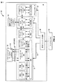
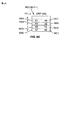
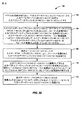
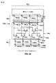
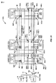
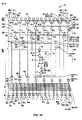
[0076]この関連で、図2は、ベクトル処理エンジン(VPE)22とも呼ばれる例示的なベクトル処理ユニット22を含むベースバンドプロセッサ20の概略図である。下記でより詳細に説明されるように、VPE22は、実行ユニット84と、本明細書で開示される例示的なベクトル処理動作を含むベクトル処理動作を提供する他の特定の例示的な回路および機能とを含む。ベースバンドプロセッサ20およびそのVPE22は、半導体ダイ24内に設けられ得る。この実施形態では、下記でより詳細に説明されるように、ベースバンドプロセッサ20は、様々なプログラム可能なデータパス構成を提供するためにプログラムされ得るプログラム可能なデータパス26を含む共通のVPE22を含む。このようにして、VPE22内の実行ユニット84とベクトルデータファイル82との間のプログラム可能なデータパス26は、ベースバンドプロセッサ20内に別々のVPE22を設ける必要なしに、様々な動作モードで様々な特定のタイプのベクトル処理動作を提供するようにプログラムおよび再プログラムされ得る。
In this regard, FIG. 2 is a schematic diagram of a
[0077]図3で始まる効率的な処理について、この開示におけるVPE22によって提供されるように構成された特定の回路とベクトル処理動作とを説明する前に、図2のベースバンドプロセッサ20の構成要素が最初に記載される。この非限定的な例におけるベースバンドプロセッサ20は、512ビットベクトルプロセッサである。ベースバンドプロセッサ20は、ベースバンドプロセッサ20内のベクトル処理を提供するVPE22をサポートするために、VPE22に加えて構成要素を含む。ベースバンドプロセッサ20は、ベクトルユニットデータメモリ(LMEM)32からベクトルデータ30を受信し記憶するように構成された、ベクトルデータファイル82としても知られる、ベクトルレジスタを含む。たとえば、ベクトルデータ30はXビット幅であり、「X」は設計選択に従って定義される(たとえば、512ビット)。ベクトルデータ30は、ベクトルデータサンプルセット34に分割され得る。非限定的な例として、ベクトルデータ30は256ビット幅であり得るし、より小さいベクトルデータサンプルセット34(Y)〜34(0)を備える場合がある。いくつかのベクトルデータサンプルセット34(Y)〜34(0)は、例として16ビット幅であり得るし、ベクトルデータサンプルセット34(Y)〜34(0)の他は、32ビット幅であり得る。VPE22は、高度の並列性を達成するために、VPE22に並列に供給されるいくつかの選ばれたベクトルデータサンプルセット34(Y)〜34(0)に対するベクトル処理を提供することが可能である。ベクトルデータファイル82はまた、VPE22がベクトルデータ30を処理するときに生成される結果を記憶するように構成される。いくつかの実施形態では、VPE22は、より速いベクトル命令実行時間を提供するようにレジスタ書込みを低減するために、ベクトルデータファイル82内に中間ベクトル処理結果を記憶しないように構成される。この構成は、スカラー処理デジタル信号プロセッサ(DSP)などの、レジスタに中間結果を記憶するスカラー処理エンジンによって実行されるスカラー命令とは反対である。
[0077] Before describing the specific circuitry and vector processing operations configured to be provided by the
[0078]図2のベースバンドプロセッサ20は、ベクトル命令の条件付き実行において使用するためにVPE22に条件を与えるように、およびベクトル命令実行の結果として更新された条件を記憶するように構成された条件レジスタ36も含む。ベースバンドプロセッサ20はまた、累算レジスタ38と、グローバルレジスタを含むグローバルレジスタファイル40と、アドレスレジスタ42とを含む。累算レジスタ38は、ベクトルデータ30に対していくつかの特殊な演算を実行する結果として累算された結果を記憶するために、VPE22によって使用されるように構成される。グローバルレジスタファイル40は、VPE22によってサポートされるいくつかのベクトル命令のためのスカラーオペランドを記憶するように構成される。アドレスレジスタ42は、ベクトルユニットデータメモリ32からベクトルデータ30を取り出し、ベクトルユニットデータメモリ32にベクトル処理結果を記憶するために、ベクトルロードによってアドレス指定可能なアドレスを記憶し、VPE22によってサポートされる命令を記憶するように構成される。
[0078] The
[0079]引き続き図2を参照すると、この実施形態におけるベースバンドプロセッサ20は、VPE22によって提供されるベクトル処理に加えて、ベースバンドプロセッサ20においてスカラー処理を提供する(「整数ユニット」とも呼ばれる)スカラープロセッサ44も含む。高効率演算のために実行される命令のタイプに基づいて、ベクトル命令演算とスカラー命令演算の両方をサポートするように構成された中央処理装置(CPU)を設けることが望ましい場合がある。この実施形態では、スカラープロセッサ44は、非限定的な例として、32ビット縮小命令セットコンピューティング(RISC)スカラープロセッサである。スカラープロセッサ44は、この例では、スカラー命令処理をサポートするための算術論理ユニット(ALU)46を含む。ベースバンドプロセッサ20は、プログラムメモリ50から命令をフェッチし、フェッチされた命令を復号し、命令タイプに基づいて、スカラープロセッサ44に、またはベクトルデータパス53を通ってVPE22に、フェッチされた命令を向けるように構成された命令ディスパッチ回路48を含む。スカラープロセッサ44は、スカラー命令を実行するときにスカラープロセッサ44によって使用される汎用レジスタ54を含む。スカラー命令実行のためにスカラープロセッサ44によるアクセス用に、メインメモリから汎用レジスタ54にデータを供給するように、整数ユニットデータメモリ(DMEM)56がベースバンドプロセッサ20に含まれる。DMEM56は、非限定的な例としてキャッシュメモリであり得る。ベースバンドプロセッサ20は、メモリコントローラデータパス62を通ってメインメモリへのアクセスを求めるベクトル命令をスカラープロセッサ44が実行しているときに汎用レジスタ54からメモリアドレスを受信するように構成されたメモリコントローラレジスタ60を含むメモリコントローラ58も含む。
[0079] With continued reference to FIG. 2, the
[0080]VPE22によるベクトル命令処理によってサポートされることが望ましい場合がある特殊ベクトル処理動作の1つのタイプは、フィルタリングである。フィルタ動作は、サンプリングされた入力時間関数の重畳の量子化時間領域表現と、フィルタの重み付け関数の表現とを計算する。時間領域内の重畳は、周波数領域内の乗算に対応する。このように、デジタルフィルタは、間隔が均一なサンプル間隔で実行される乗算および加算の拡張シーケンスにより、VPE22において実現され得る。たとえば、ディスクリート有限インパルス応答(FIR)フィルタは、フィルタ関数を計算するために、「Y」計算フィルタ係数を有する遅延線上の遅延タップの有限数(Y)を使用して実施され得る。
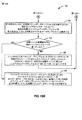
[0080] One type of special vector processing operation that may be desired to be supported by vector instruction processing by the
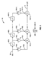
[0081]この関連で、図3は、図2のVPE22におけるフィルタベクトル処理動作を介してサポートされることが望ましい場合がある、例示的なディスクリートFIRフィルタ64の概略図である。デジタル化入力信号66(x[n])は、「フィルタ遅延タップ」68(1)〜68(Y−1)と呼ばれる遅延構造を通ってデジタル化入力信号サンプル(x[0],x[1],...x[n])を渡すことによってフィルタリングされ得る。フィルタ遅延タップ68(1)〜68(Y−1)は、フィルタサンプル被乗数72(0)〜72(Y−1)を供給するために、すべてのデジタル化入力信号サンプル(すなわち、x[0],x[1],...x[n])が各々フィルタ係数(h[0]〜h(Y−1))によって乗算される(すなわち、h(l)*x[n−l])ために、クロックされたデジタル化入力信号サンプル(すなわち、x[0],x[1],...x[n])を乗算器70(0)〜70(Y−1)の中にシフトする。フィルタサンプル被乗数72(0)〜72(Y−1)は、結果として生じるフィルタ処理された出力信号76(すなわち、y[n])を供給するために、加算器(すなわち、アダー)74(1)〜74(Y−1)によって一緒に加算される。このように、図3のディスクリートFIRフィルタ64は以下のように要約され得る。
[0081] In this regard, FIG. 3 is a schematic diagram of an exemplary
![]()
![]()
ここで、
nは入力信号サンプルの数であり、
x[n]はデジタル化入力信号66であり、
y[n]は、結果として生じるフィルタ処理された出力信号76であり、
h(l)はフィルタ係数であり、
Yはフィルタ係数の数である。
フィルタ係数h(l)は複素数であり得る。一態様では、VPE22は、(たとえば、グローバルレジスタファイル40から)フィルタ係数を受信することができる。VPE22は、FIRフィルタ関数を実行するために受信されたフィルタ係数を直接使用することができ、その場合、上記の式におけるフィルタ係数h(l)は、受信されたフィルタ係数を表すことができる。代替として、VPE22は、FIRフィルタ関数を実行するためにそれらを使用する前に、受信されたフィルタ係数の複素共役を計算することができ、その場合、上記の式におけるフィルタ係数h(l)は、受信されたフィルタ係数の共役を表すことができる。
here,
n is the number of input signal samples,
x [n] is the digitized
y [n] is the resulting filtered output signal 76;
h (l) is a filter coefficient,
Y is the number of filter coefficients.
The filter coefficient h (l) can be a complex number. In one aspect,
[0082]図3の上記のディスクリートFIRフィルタ64は、以下のように書き直され得る。
y[n]=x[n]*h0+x[n−1]*h1+...+x[n−7]*h7
[0082] The
y [n] = x [n] * h0 + x [n-1] * h1 +. . . + X [n-7] * h7
[0083]しかしながら、図3のディスクリートFIRフィルタ64などのフィルタリング演算は、ベクトルプロセッサにおいて提供される特殊データフローパスに起因して、ベクトルプロセッサにおいて並列化することは困難であり得る。フィルタリングされるべき入力ベクトルデータサンプルセット(たとえば、ベクトル化されたデジタル化入力信号66)が、フィルタ遅延タップ(たとえば、68(1)〜68(Y−1))の間でシフトされると、入力ベクトルデータサンプルセットはベクトルデータファイルから再フェッチされ、したがって電力消費が増大し、スループットが低減される。ベクトルデータファイルからの入力ベクトルデータサンプルセットの再フェッチを最小化するために、ベクトルプロセッサ内のデータフローパスは、効率的な並列化処理のために、フィルタ遅延タップ(たとえば、68(1)〜68(Y−1))と同じ数の乗算器(たとえば、70(0)〜70(Y−1))を設けるように構成される可能性がある。しかしながら、他のベクトル処理動作は、より少ない乗算器しか必要としない場合があり、それにより、データフローパス内の乗算器の非効率的なスケーリングおよび過少利用がもたらされる。スケーラビリティを提供するために、乗算器の数がフィルタ遅延タップの数よりも少なくなるように削減された場合、フィルタ処理の様々なフェーズに対して同じ入力ベクトルデータサンプルセットを取得するために、メモリにより多くの再フェッチが必要とされることによって、並列化が制限される。
[0083] However, filtering operations such as the
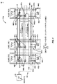
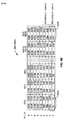
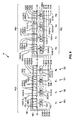
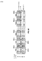
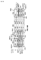
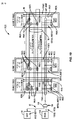
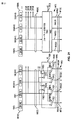
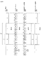
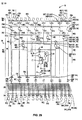
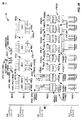
[0084]この関連で、図4は、図2のVPE22として提供され得る例示的なVPE22(1)の概略図である。下記でより詳細に記載されるように、図4のVPE22(1)は、ベクトルデータサンプルの再フェッチが除去または低減され、電力消費が低減される、VPE22(1)内の精度フィルタベクトル処理動作を提供する。精度フィルタベクトル処理動作は、ベクトルデータサンプルの再フェッチを必要とし、それにより結果として電力消費が増大する、中間結果の記憶を必要とするフィルタベクトル処理動作と比較して、VPE22(1)において提供され得る。ベクトルデータファイルからの入力ベクトルデータサンプルの再フェッチを除去または最小化して、電力消費を低減し、処理効率を改善するために、VPE22(1)内のベクトルデータファイル82(0)〜82(X)と(「EU」とも標記される)実行ユニット84(0)〜84(X)との間の入力データフローパス80(0)〜80(X)にタップ付き遅延線78が含まれる。「X」+1は、この例におけるベクトルデータサンプルの処理用にVPE22(1)内に設けられる並列入力データレーンの最大数である。タップ付き遅延線78は、ベクトルデータファイル82(0)〜82(X)の対応するサブセットまたはすべてから入力ベクトルデータサンプルセット86(0)〜86(X)の入力ベクトルデータサンプル86のサブセットまたはすべてとして、タップ付き遅延線入力88(0)〜88(X)上で入力ベクトルデータサンプルセット86(0)〜86(X)を受信するように構成される。入力ベクトルデータサンプルセット86(0)〜86(X)は、この例では86(0)、86(1)、...、および86(X)である、「X+1」個の入力ベクトルデータサンプル86から構成される。
[0084] In this regard, FIG. 4 is a schematic diagram of an exemplary VPE 22 (1) that may be provided as
[0085]引き続き図4を参照すると、タップ付き遅延線78は、フィルタベクトル処理動作のために実行ユニット84(0)〜84(X)によって処理されるべき、ベクトルデータファイル82(0)〜82(X)からフェッチされた入力ベクトルデータサンプルセット86(0)〜86(X)を記憶する。下記の図6および図7に関して下記でより詳細に説明されるように、タップ付き遅延線78は、実行ユニット84(0)〜84(X)にシフトされた入力ベクトルデータサンプルセット86S(0)〜86S(X)を供給するために、VPE22(1)によって実行されるべきフィルタベクトル命令に従うフィルタベクトル処理動作のフィルタ遅延タップ(すなわち、フィルタ処理ステージ)ごとに、入力ベクトルデータサンプルセット86(0)〜86(X)をシフトするように構成される。シフトされた入力ベクトルデータサンプル86Sのすべては、シフトされた入力ベクトルデータサンプルセット86S(0)〜86S(X)を備える。タップ付き遅延線78は、フィルタベクトル処理動作中、実行ユニット84(0)〜84(X)の実行ユニット入力90(0)〜90(X)にシフトされた入力ベクトルデータサンプル86S(0)〜86S(X)を供給する。このようにして、フィルタベクトル処理動作のフィルタタップのためのシフトされた入力ベクトルデータサンプルセット86S(0)〜86S(X)に対して実行される動作に基づく中間フィルタ結果は、VPE22(1)によって実行されるフィルタベクトル処理動作の各処理ステージの間、記憶、シフト、およびベクトルデータファイル82(0)〜82(X)から再フェッチされる必要がない。このように、タップ付き遅延線78は、VPE22(1)によって実行されるフィルタベクトル処理動作についての電力消費を低減し、処理効率を上げることができる。
[0085] With continued reference to FIG. 4, tapped
[0086]「ベクトル処理ステージ」とも呼ばれるVPE22(1)内の処理ステージは、特定のタスクまたは動作を実行するように設計された回路と関連するベクトルデータパスとを備える。ベクトル処理動作は、いくつかの異なる処理ステージにおいて、VPE22(1)によって実行される場合がある。各処理ステージは、VPE22(1)の1つまたは複数のクロックサイクルにわたって実行される場合がある。その結果、VPE22(1)内のベクトル処理動作の実行は、ベクトル処理動作の各処理ステージが各々1つまたは複数のクロックサイクルを消費する可能性があるので、完了するために多くのクロックサイクルを要する可能性がある。たとえば、処理ステージは、図4のVPE22(1)内のタップ付き遅延線78の中に入力ベクトルデータサンプルセット86(0)〜86(X)をフェッチすることを含む場合がある。VPE22(1)内のベクトル処理ステージはパイプライン化され得る。
[0086] A processing stage within VPE 22 (1), also referred to as a "vector processing stage", comprises a vector data path associated with circuitry designed to perform a particular task or operation. Vector processing operations may be performed by VPE 22 (1) at several different processing stages. Each processing stage may be executed over one or more clock cycles of VPE 22 (1). As a result, execution of vector processing operations in VPE 22 (1) may take many clock cycles to complete because each processing stage of the vector processing operations may consume one or more clock cycles each. It may take. For example, the processing stage may include fetching input vector data sample sets 86 (0) -86 (X) into the tapped
[0087]実行ユニット84(0)〜84(X)は、フェッチされた入力ベクトルデータサンプルセット86(0)〜86(X)を処理する1つまたは複数のパイプラインステージを含む場合がある。たとえば、実行ユニット84(0)〜84(X)内の1つのパイプラインステージは、累算演算を実行するように構成された累算器から構成される累算ステージを含む場合がある。別の例として、実行ユニット84(0)〜84(X)内の別のパイプラインステージは、乗算演算を実行するように構成された乗算器から構成される乗算ステージを含む場合がある。 [0087] Execution units 84 (0) -84 (X) may include one or more pipeline stages that process fetched input vector data sample sets 86 (0) -86 (X). For example, one pipeline stage in execution units 84 (0) -84 (X) may include an accumulation stage comprised of accumulators configured to perform accumulation operations. As another example, another pipeline stage in execution units 84 (0) -84 (X) may include a multiplication stage comprised of multipliers configured to perform multiplication operations.
[0088]引き続き図4を参照すると、実行ユニット84(0)〜84(X)は、フィルタベクトル処理動作のための図2のグローバルレジスタファイル40に記憶されたフィルタ係数92(0)〜92(Y−1)の中からフィルタ係数92を受信する、ここで、「Y」はフィルタベクトル処理動作のためのフィルタ係数の数に等しい場合がある。実行ユニット84(0)〜84(X)は、各々、実行ユニット84(0)〜84(X)内に中間フィルタベクトルデータ出力サンプルを供給するために、ベクトルフィルタ処理動作の各処理ステージの間に、受信されたフィルタ係数92(0)、90(1)、...90(Y−1)のうちの1つを、シフトされた入力ベクトルデータサンプルセット86S(0)〜86S(X)のシフトされた入力ベクトルデータサンプル86S(0)、86S(1)、...86S(X)と乗算するように構成される。中間フィルタベクトルデータ出力サンプルセットは、実行ユニット84(0)〜84(X)の各々において累算される(すなわち、前に累算されたフィルタ出力ベクトルデータサンプルが現在の累算されたフィルタ出力ベクトルデータサンプルに加算される)。これにより、シフトされた入力ベクトルデータサンプルセット86S(0)〜86S(X)内のシフトされた入力ベクトルデータサンプル86S(0)、86S(1)、...86S(X)ごとに、それぞれ、出力データフローパス98(0)〜98(X)上の実行ユニット出力96(0)〜96(X)上に実行ユニット84(0)〜84(X)によって供給される、最終的な、結果として生じるフィルタ出力ベクトルデータサンプルセット94(0)〜94(X)がもたらされる。結果として生じるフィルタ出力ベクトルデータサンプルセット94(0)〜94(X)は、この例では94(0)、94(1)、...、および94(X)である、「X+1」個の、結果として生じるフィルタ出力ベクトルデータサンプル94から構成される。実行ユニット84(0)〜84(X)によって生成された中間フィルタベクトルデータ出力サンプルセットを記憶しシフトする必要なしに、結果として生じるフィルタ出力ベクトルデータサンプルセット94(0)〜94(X)は、VPE22(1)によるさらなる使用および/または処理のために、それぞれのベクトルデータファイル82(0)〜82(X)に戻されて記憶される。
[0088] With continued reference to FIG. 4, execution units 84 (0) -84 (X) receive filter coefficients 92 (0) -92 () stored in
[0089]引き続き図4を参照すると、下記でより詳細に説明されるように、タップ付き遅延線78は、処理されているベクトル命令に従って制御されるようにプログラム可能である。フィルタベクトル命令が処理されていない場合、タップ付き遅延線78は、ベクトルデータファイル82(0)〜82(X)と実行ユニット84(0)〜84(X)との間の入力データフローパス80(0)〜80(X)に含まれないようにプログラムされ得る。この実施形態では、タップ付き遅延線78は、フィルタベクトル処理動作のフィルタタップごとにシフトされた入力ベクトルデータサンプルセット86S(0)〜86S(X)を供給するために、ベクトルデータファイル82(0)〜82(X)から受信された入力ベクトルデータサンプルセット86(0)〜86(X)をロードしシフトするように構成される。このように、シフトされた入力ベクトルデータサンプルセット86S(0)〜86S(X)は、フィルタベクトル処理動作のフィルタタップの実行のために、実行ユニット84(0)〜84(X)に供給され得る。タップ付き遅延線78がないと、フィルタベクトル処理動作の次のフィルタタップのために、実行ユニット84(0)〜84(X)にシフトされた中間入力ベクトルデータサンプルセットを再び供給するために、別個のシフティングプロセスが実行される必要があるはずであり、それにより、遅延時間が増大し、さらなる電力が消費される。さらに、フィルタベクトル処理動作中、ベクトルデータファイル82(0)〜82(X)からのシフトされた入力ベクトルデータサンプルセット86S(0)〜86S(X)の再フェッチ遅延によって、VPE22(1)内の入力データフローパス80(0)〜80(X)および出力データフローパス98(0)〜98(X)の効率が制限される。
[0089] With continued reference to FIG. 4, the tapped
[0090]シフトされた入力ベクトルデータサンプルセット86S(0)〜86S(X)は、実行ユニット84(0)〜84(X)に局在するタップ付き遅延線78によって供給される。実行ユニット84(0)〜84(X)におけるベクトル処理は、データフローの制限ではなく、コンピュータリソースのみによって制限される。これは、シフトされた入力ベクトルデータサンプルセット86S(0)〜86S(X)がベクトルデータファイル82(0)〜82(X)からフェッチされるまで待つ必要なしに、実行ユニット84(0)〜84(X)が、ベクトル処理動作を実行するためにシフトされた入力ベクトルデータサンプルセット86S(0)〜86S(X)を受信することに、連続して、または実質的に連続して忙しいことを意味する。
[0090] The shifted input vector data sample sets 86S (0) -86S (X) are provided by a tapped
[0091]さらに、図4のVPE22(1)によって実行されるフィルタベクトル処理動作は、タップ付き遅延線78を利用することによってより精密になり得るが、これは、実行ユニット84(0)〜84(X)内の中間フィルタ処理ステージのための出力累算がベクトルデータファイル82(0)〜82(X)に記憶される必要がないからである。実行ユニット84(0)〜84(X)からベクトルデータファイル82(0)〜82(X)への中間出力ベクトルデータサンプルセットの記憶は、丸めをもたらす可能性がある。したがって、次の中間出力ベクトルデータサンプルセットがベクトル処理動作のために実行ユニット84(0)〜84(X)に供給されるとき、ベクトル処理動作の各乗算フェーズの間に任意の丸め誤差が伝搬および加算される。対照的に、図4のVPE22(1)の例では、実行ユニット84(0)〜84(X)によって計算された中間出力ベクトルデータサンプルセットは、ベクトルデータファイル82(0)〜82(X)に記憶される必要がない。実行ユニット84(0)〜84(X)は、前の中間出力ベクトルデータサンプルセットを次のフィルタ遅延タップのための中間出力ベクトルデータサンプルセットと累算することができるが、これは、タップ付き遅延線78が、処理されるべきベクトル処理動作の間に、実行ユニット84(0)〜84(X)にシフトされた入力ベクトルデータサンプルセット86S(0)〜86S(X)を供給するからであり、結果は前のフィルタ遅延タップのための前のベクトルデータサンプルセットと累算される。
[0091] In addition, the filter vector processing operations performed by VPE 22 (1) of FIG. This is because the output accumulation for the intermediate filtering stage in (X) need not be stored in vector data files 82 (0) -82 (X). Storage of the intermediate output vector data sample sets from execution units 84 (0) -84 (X) to vector data files 82 (0) -82 (X) may result in rounding. Thus, when the next intermediate output vector data sample set is fed to execution units 84 (0) -84 (X) for vector processing operations, any rounding errors are propagated and propagated during each multiplication phase of the vector processing operations. Is added. In contrast, in the VPE 22 (1) example of FIG. 4, the intermediate output vector data sample sets computed by execution units 84 (0) -84 (X) are vector data files 82 (0) -82 (X). Need not be memorized. Execution units 84 (0) -84 (X) may accumulate the previous intermediate output vector data sample set with the intermediate output vector data sample set for the next filter delay tap, which is tapped. Because
[0092]引き続き図4を参照すると、この実施形態におけるVPE22(1)は、並列化処理のための(VLANE0 100(0)〜VLANEX 100(X)と標記された)複数のベクトルデータレーンから構成される。各ベクトルデータレーン100(0)〜100(X)は、この実施形態では、ベクトルデータファイル82と実行ユニット84とを含んでいる。例としてベクトルデータレーン100(0)を取り上げると、その中のベクトルデータファイル82(0)は、フィルタベクトル処理のために実行ユニット84(0)によって受信されるように、入力データフローパス80(0)上に入力ベクトルデータサンプル86(0)を供給するように構成される。上記で説明されたように、タップ付き遅延線78は、フィルタベクトル処理のために、入力ベクトルデータサンプル86(0)をシフトし、シフトされた入力ベクトルデータサンプル86S(0)を実行ユニット84(0)に供給するために、入力データフローパス80(0)内に設けられる。ベクトルデータファイル82(0)はまた、VPE22(1)によって処理されるべき現在または次のベクトル命令に従って、必要または所望に応じて、次のベクトル処理動作のためにベクトルデータファイル82(0)に戻されて記憶されるべき、出力データフローパス98(0)からのフィルタベクトル処理の結果として、実行ユニット84(0)によって供給される、結果として生じるフィルタ出力ベクトルデータサンプル94(0)を受信するように構成される。
[0092] With continued reference to FIG. 4, the VPE 22 (1) in this embodiment is comprised of a plurality of vector data lanes (labeled VLANE0 100 (0) to VLANEX 100 (X)) for parallel processing. Is done. Each vector data lane 100 (0) -100 (X) includes a vector data file 82 and an
[0093]必要に応じて、任意の数のベクトルデータレーン100(0)〜100(X)がVPE22(1)内に設けられる場合がある。VPE22(1)内に設けられるベクトルデータレーン100(0)〜100(X)の数は、効率目的のための並列化ベクトル処理対さらなるベクトルデータレーン100(0)〜100(X)を設けることに伴うさらなる回路、空間、および電力消費についてのトレードオフに基づく場合がある。1つの非限定的な例として、16個のベクトルデータレーン100がVPE22(1)内に設けられる場合があり、各ベクトルデータレーン100は、VPE22(1)内の512ビットまでのベクトルデータの並列化処理を提供するために、32ビットのデータ幅能力を有する。
[0093] Any number of vector data lanes 100 (0) -100 (X) may be provided in VPE 22 (1) as needed. The number of vector data lanes 100 (0) -100 (X) provided in VPE 22 (1) provides parallel vector processing vs. further vector data lanes 100 (0) -100 (X) for efficiency purposes. May be based on additional circuit, space, and power consumption tradeoffs. As one non-limiting example, 16
[0094]引き続き図4を参照すると、すべてのベクトルデータファイル82(0)〜82(X)に適用可能であるが、例としてベクトルデータレーン100(0)内のベクトルデータファイル82(0)を使用して、ベクトルデータファイル82(0)により、入力ベクトルデータサンプル86(0)の1つまたは複数のサンプルがベクトル処理のために記憶されることが可能になる。VPE22(1)によって実行されている特定のベクトル命令に従う入力ベクトルデータサンプル86(0)のプログラミングに応じて、入力ベクトルデータサンプル86(0)の幅が設けられる。入力データフローパス80(0)の幅は、所与のベクトル命令がタップ付き遅延線78および実行ユニット84(0)に様々な幅の入力ベクトルデータサンプル86(0)を供給するために、クロックサイクルごとを含むベクトル命令ごとにプログラム可能および再プログラム可能である。このようにして、ベクトルデータレーン100(0)は、実行されているベクトル命令のタイプに応じて、入力ベクトルデータサンプル86(0)の様々な幅の処理を提供するように、プログラムおよび再プログラムされ得る。
[0094] Continuing to refer to FIG. 4, it is applicable to all vector data files 82 (0) -82 (X), but as an example the vector data file 82 (0) in the vector data lane 100 (0) In use, the vector data file 82 (0) allows one or more samples of the input vector data sample 86 (0) to be stored for vector processing. Depending on the programming of the input vector data sample 86 (0) according to the particular vector instruction being executed by the VPE 22 (1), the width of the input vector data sample 86 (0) is provided. The width of the input data flow path 80 (0) is determined by the number of clock cycles for a given vector instruction to provide input vector data samples 86 (0) of varying widths to the tapped
[0095]たとえば、ベクトルデータファイル82(0)は、32ビット幅であり、同様に32ビットまでの幅である入力ベクトルデータサンプル86を記憶することが可能であり得る。入力ベクトルデータサンプル86(0)は、ベクトルデータファイル82(0)の幅全体(たとえば、32ビット)を消費する場合があるか、またはベクトルデータファイル82(0)の幅のより小さいサンプルサイズで供給される場合がある。入力ベクトルデータサンプル86(0)のサイズは、VPE22(1)によって実行されているベクトル命令に基づく、入力ベクトルデータサンプル86(0)のサイズ向けの入力データフローパス80(0)の構成のプログラミングに基づいて構成され得る。たとえば、入力ベクトルデータサンプル86(0)は、1つのベクトル命令のための2つの別々の16ビットベクトルデータサンプルを備える場合がある。別の例として、入力ベクトルデータサンプル86(0)は、1つの32ビットベクトルデータサンプルとは対照的に、別のベクトル命令のためのベクトルデータファイル82(0)内の4つの8ビットベクトルデータサンプルを備える場合がある。別の例では、入力ベクトルデータサンプル86(0)は、1つの32ビットベクトルデータサンプルを備える場合がある。VPE22(1)はまた、ベクトル命令ごとに、および/または所与のベクトル命令のクロックサイクルごとに、実行ユニット84(0)によりベクトルデータファイル82(0)に供給される様々なサイズの、結果として生じるフィルタ出力ベクトルデータサンプル94(0)を受信するように、ベクトルデータファイル82(0)のための出力データフローパス98(0)をプログラムおよび再プログラムすることが可能である。
[0095] For example, the vector data file 82 (0) is 32 bits wide and may be capable of storing input
[0096]図4のVPE22(1)のさらなる詳細および特徴、ならびにこの実施形態における入力データフローパス80(0)〜80(X)内の実行ユニット84(0)〜84(X)にシフトされた入力ベクトルデータサンプルセット86S(0)〜86S(X)を供給するためのタップ付き遅延線78のさらなる説明が次に記載される。この関連で、図5は、例示的なフィルタベクトル命令に従って、タップ付き遅延線78を利用する図4のVPE22(1)において実行され得る例示的なフィルタベクトル処理動作102を示すフローチャートである。図6A〜図10において提供される例を参照して、図5のフィルタベクトル処理動作102において実行される例示的なタスクが記載される。
[0096] Further details and features of VPE 22 (1) in FIG. 4 and shifted to execution units 84 (0) -84 (X) in input data flow paths 80 (0) -80 (X) in this embodiment. Further description of tapped
[0097]図5を参照すると、フィルタベクトル命令に従ってフィルタベクトル処理動作102において処理されるべき入力ベクトルデータサンプルセット86(0)〜86(X)は、フィルタベクトル処理動作102のために、ベクトルデータファイル82(0)〜82(X)から入力データフローパス80(0)〜80(X)の中にフェッチされる(ブロック104)。図4のVPE22(1)に関して上記で説明されたように、入力ベクトルデータサンプルセット86(0)〜86(X)は、実行ユニット84(0)〜84(X)内のグローバルレジスタファイル40から受信されたフィルタ係数92(0)〜92(Y−1)と乗算される。たとえば、図6Aは、グローバルレジスタファイル40内のフィルタ係数92(0)〜92(Y−1)(すなわち、h7〜h0)を示す。この例では、実行されるべきフィルタベクトル処理動作102において8個のフィルタタップを提供する、グローバルレジスタファイル40に記憶された8個のフィルタ係数92が存在する。この例では、上記で説明された図3のディスクリートFIRフィルタ64の式からのフィルタベクトル処理動作102は、下記の通りであることに留意されたい。
y[n]=x[n]*h0+x[n−1]*h1+...+x[n−7]*h7
[0097] Referring to FIG. 5, the input vector data sample sets 86 (0) -86 (X) to be processed in the filter
y [n] = x [n] * h0 + x [n-1] * h1 +. . . + X [n-7] * h7
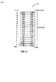
[0098]図6Bは、フィルタベクトル処理動作102によってフィルタリングされるべき入力信号を表す、図4のVPE22(1)内のベクトルデータファイル82(0)〜82(X)に記憶された例示的な入力ベクトルデータサンプルセット86(0)〜86(X)を示す。この例では、サンプルX0は最も古いサンプルであり、サンプルX63はつい最近のサンプルである。言い換えれば、この例では、サンプルX63は、時間的にサンプルX0の後に発生する。ベクトルデータファイル82(0)〜82(X)の各アドレスは16ビット幅であるので、ベクトルデータファイル82(0)〜82(X)に記憶された最初の入力ベクトルデータサンプルセット86(0)〜86(X)は、図6Bに示されたように、ADDRESS0およびADDRESS1にまたがる。これにより、ベクトルデータファイル82(0)〜82(X)が、図4のVPE22(1)の例における実行ユニット84(0)〜84(X)の32ビット幅能力をサポートするために、32ビット幅の入力ベクトルデータサンプル86を供給することが可能になる。この関連で、最初の入力ベクトルデータサンプルセット86(0)〜86(X)を備える、合計512ビットの各々8ビットの幅である64個の合計入力ベクトルデータサンプルサブセット(すなわち、X0〜X63)が存在する。同様に、ADDRESS2およびADDRESS3は、ベクトルデータファイル82(0)〜82(X)に記憶された別の2番目の入力ベクトルデータサンプルセット86(0)〜86(X)を記憶する。図6Bのこの例では、各ベクトルデータファイル82(0)〜82(X)の8個のアドレス(ADDRESS0〜7)が示され、256個の合計入力ベクトルデータサンプル86(すなわち、X0〜X255)を示すが、それは限定的でないことに留意されたい。
[0098] FIG. 6B illustrates an exemplary stored in vector data files 82 (0) -82 (X) in VPE 22 (1) of FIG. 4 that represents the input signal to be filtered by the filter
[0099]フィルタベクトル処理動作102に関与する入力ベクトルデータサンプルセット86(0)〜86(X)の幅に応じて、ベクトル命令のプログラミングに従うフィルタベクトル処理動作102を提供するために、図4のVPE22(1)内のベクトルデータレーン100(0)〜100(X)の1つ、いくつか、またはすべてが利用され得る。ベクトルデータファイル82(0)〜82(X)の幅全体が必要な場合、すべてのベクトルデータレーン100(0)〜100(X)がフィルタベクトル処理動作102に利用され得る。フィルタベクトル処理動作102は、フィルタベクトル処理動作102に利用され得るベクトルデータレーン100(0)〜100(X)のサブセットを必要とするにすぎない場合があることに留意されたい。これは、入力ベクトルデータサンプルセット86(0)〜86(X)の幅がすべてのベクトルデータファイル82(0)〜82(X)の幅よりも小さいからであり得るし、ここで、フィルタベクトル処理動作102と並列に実行されるべき他のベクトル処理動作にさらなるベクトルデータレーン100を利用することが望ましい。現在の例を説明する目的で、フィルタベクトル処理動作102において利用される入力ベクトルデータサンプルセット86(0)〜86(X)が、すべてのベクトルデータレーン100(0)〜100(X)を要すると想定する。
[0099] To provide a filter
[00100]図5に戻って参照すると、現在の入力ベクトルデータサンプルセット86(0)〜86(X)としてタップ付き遅延線78にロードされるために、フェッチされた入力ベクトルデータサンプルセット86(0)〜86(X)が、ベクトルデータファイル82(0)〜82(X)から入力データフローパス80(0)〜80(X)に供給される(ブロック106)。入力ベクトルデータサンプルセット86(0)〜86(X)は、フィルタベクトル処理動作102のために実行ユニット84(0)〜84(X)によって処理されるべき入力ベクトルデータサンプルセット86(0)〜86(X)として、プライマリタップ付き遅延線78(0)の中にロードされる。プライマリタップ付き遅延線78(0)の中にロードされた入力ベクトルデータサンプルセット86(0)〜86(X)は、フィルタベクトル処理動作102の最初のフィルタタップ動作のためにシフトされない。しかしながら、上記で説明され、図7に関して下記でさらに詳細に説明されるように、タップ付き遅延線78の目的は、フィルタベクトル処理動作102の次のフィルタタップ動作のために実行ユニット84(0)〜84(X)にシフトされた入力ベクトルデータサンプルセット86S(0)〜86S(X)を供給するために、入力ベクトルデータサンプルセット86(0)〜86(X)のシフトを提供することである。実行ユニット84(0)〜84(X)によって実行されるフィルタベクトル処理動作102の各処理ステージの間、実行ユニット84(0)〜84(X)にシフトされた入力ベクトルデータサンプルセット86S(0)〜86S(X)を供給するために、入力ベクトルデータサンプル86がプライマリタップ付き遅延線78(0)内でシフトされる。このようにして、入力ベクトルデータサンプルセット86(0)〜86(X)は、フィルタベクトル処理動作102のフィルタタップ動作ごとに、記憶、ベクトルデータファイル82(0)〜82(X)内でシフト、および再フェッチされる必要がない。
[00100] Referring back to FIG. 5, the fetched input vector data sample set 86 () is loaded into the tapped
[00101]オプションのシャドウタップ付き遅延線78(1)がVPE22(1)内に設けられた場合、次の入力ベクトルデータサンプルセット86N(0)〜86N(X)も、ベクトルデータファイル82(0)〜82(X)からシャドウタップ付き遅延線78(1)の中にロードされ得る。図7に関して下記でさらに詳細に説明されるように、次の入力ベクトルデータサンプルセット86N(0)〜86N(X)は、シフトされた入力ベクトルデータサンプルセット86S(0)〜86S(X)の少なくとも一部になるために、フィルタベクトル処理動作102の間にプライマリタップ付き遅延線78(0)の中にシフトされる。このように、プライマリタップ付き遅延線78(0)は、フィルタベクトル処理動作102のために実行されるべき次の入力ベクトルデータサンプルセット86N(0)〜86N(X)が、ベクトルデータファイル82(0)〜82(X)からプライマリタップ付き遅延線78(0)の中にフェッチされるまで、実行ユニット84(0)〜84(X)が待つ必要があった場合、場合によっては被る遅延をフェッチすることなく、フィルタベクトル処理動作102の間に利用可能なシフトされた入力ベクトルデータサンプルセット86S(0)〜86S(X)を有することができる。
[00101] If the optional shadow-tapped delay line 78 (1) is provided in the VPE 22 (1), the next input vector data sample sets 86N (0) -86N (X) are also stored in the vector data file 82 (0). ) -82 (X) can be loaded into the shadow tapped delay line 78 (1). As described in more detail below with respect to FIG. 7, the next input vector data sample set 86N (0) -86N (X) is the same as the shifted input vector data sample set 86S (0) -86S (X). To be at least partly shifted into the primary tapped delay line 78 (0) during the filter
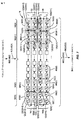
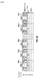
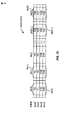
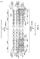
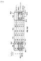
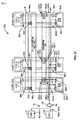
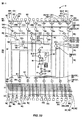
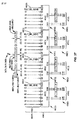
[00102]この関連で、図7は、図4のVPE22(1)内に設けられ得る例示的なタップ付き遅延線78を示す。この実施形態では、タップ付き遅延線78は、シャドウタップ付き遅延線78(1)とプライマリタップ付き遅延線78(0)とを備える。この例におけるプライマリタップ付き遅延線78(0)は、入力ベクトルデータサンプル86の解像度が8ビット長に落ちることを可能にするために、複数の8ビットプライマリパイプラインレジスタ120から構成される。実行ユニット84(0)〜84(X)によって処理される最初の入力ベクトルデータサンプルセット86(0)〜86(X)は、下記の図9Aに関して説明されるように、フィルタベクトル処理動作102の最初のフィルタタップのために、この例ではシフトされない。実行ユニット84(0)〜84(X)がフィルタベクトル処理動作102のために次のフィルタタップを処理するとき、プライマリタップ付き遅延線78(0)に記憶された入力ベクトルデータサンプルセット86(0)〜86(X)の中の入力ベクトルデータサンプル86は、シフトされた入力ベクトルデータサンプルセット86S(0)〜86S(X)になるために、図7の矢印によって示されたように、プライマリパイプラインレジスタ120(0)〜120(4X+3)内でシフトされる。このようにして、実行ユニット84(0)〜84(X)は、入力ベクトルデータサンプルセット86(0)〜86(X)を記憶およびシフトする必要なしに、ならびにベクトルデータファイル82(0)〜82(X)からシフトされた入力ベクトルデータサンプルセット86S(0)〜86S(X)を再フェッチすることなく、シフトされた入力ベクトルデータサンプルセット86S(0)〜86S(X)を受信し、それらのフィルタベクトル処理動作102を実行することによって、十分利用される。
[00102] In this regard, FIG. 7 illustrates an exemplary tapped
[00103]この実施形態では、プライマリパイプラインレジスタ120(0)〜120(4X+3)はまとめて、図4のベクトルデータファイル82(0)〜82(X)の幅である。15に等しい「X」を有する幅が512ビットであるベクトルデータファイル82(0)〜82(X)の例では、512ビット(すなわち、64個のレジスタ×各8ビット)の合計幅を提供するために、各々が8ビット幅である64個の合計プライマリパイプラインレジスタ120(0)〜120(63)が存在する。したがって、この例では、プライマリタップ付き遅延線78(0)は、1つの入力ベクトルデータサンプルセット86(0)〜86(X)の幅全体を記憶することが可能である。この例では、8ビット幅のプライマリパイプラインレジスタ120(0)〜120(4X+3)を設けることによって、入力ベクトルデータサンプルセット86(0)〜86(X)は、プライマリパイプラインレジスタ120(0)〜120(4X+3)において、8ビットフィルタベクトル処理動作のために8ビットのベクトルデータサンプルサイズにシフトダウンされ得る。たとえば、16ビットまたは32ビットのサンプルなどのより大きいサイズの入力ベクトルデータサンプル86のサイズがフィルタベクトル処理動作のために望ましい場合、入力ベクトルデータサンプルセット86(0)〜86(X)は、プライマリパイプラインレジスタ120(0)〜120(4X+3)において、1度に2つのプライマリパイプラインレジスタ120によってシフトされ得る。
[00103] In this embodiment, primary pipeline registers 120 (0) -120 (4X + 3) are collectively the width of vector data files 82 (0) -82 (X) in FIG. In the example of a vector data file 82 (0) -82 (X) having a width of “X” equal to 15 and 512 bits, it provides a total width of 512 bits (ie, 64 registers × 8 bits each) Therefore, there are 64 total primary pipeline registers 120 (0) -120 (63), each 8 bits wide. Accordingly, in this example, the primary tapped delay line 78 (0) can store the entire width of one input vector data sample set 86 (0) -86 (X). In this example, by providing 8-bit wide primary pipeline registers 120 (0) to 120 (4X + 3), the input vector data sample sets 86 (0) to 86 (X) are converted into the primary pipeline registers 120 (0). ~ 120 (4X + 3) may be shifted down to an 8-bit vector data sample size for 8-bit filter vector processing operations. For example, if a larger input
[00104]引き続き図7を参照すると、シャドウタップ付き遅延線78(1)もタップ付き遅延線78内に設けられる。シャドウタップ付き遅延線78(1)は、次のベクトル処理動作のためにベクトルデータファイル82(0)〜82(X)から次の入力ベクトルデータサンプルセット86N(0)〜86N(X)をラッチまたは輸送するために利用され得る。フィルタベクトル処理動作102のための各フィルタタップが実行ユニット84(0)〜84(X)によって実行されるとき、次の入力ベクトルデータサンプルセット86N(0)〜86N(X)からの次の入力ベクトルデータサンプル86Nは、シャドウタップ付き遅延線78(1)からプライマリタップ付き遅延線78(0)の中にシフトされる。シャドウタップ付き遅延線78(1)はまた、入力ベクトルデータサンプル86の解像度が、プライマリタップ付き遅延線78(0)と同様に8ビット長に落ちることを可能にするために、複数の8ビットシャドウパイプラインレジスタ122から構成される。プライマリパイプラインレジスタ120(0)〜120(4X+3)のように、シャドウタップ付き遅延線78(1)内に設けられたシャドウパイプラインレジスタ122(0)〜122(4X+3)はまとめて、この例では512ビットである、ベクトルデータファイル82(0)〜82(X)の幅である。したがって、シャドウタップ付き遅延線78(1)のシャドウパイプラインレジスタ122(0)〜122(4X+3)も、1つの入力ベクトルデータサンプルセット86(0)〜86(X)の幅全体を記憶することが可能である。したがって、この実施形態では、プライマリタップ付き遅延線78(0)に含まれるシャドウパイプラインレジスタ122(0)〜122(4X+3)の数は、この例では合計16である(すなわち、X=15)ベクトルデータレーン100(0)〜100(X)の数の4倍である。したがって、シャドウパイプラインレジスタ122の数も、合計512ビット(すなわち、64個のレジスタ×各8ビット)向けにこの例では合計64である。プライマリタップ付き遅延線78(0)に関して上記で説明されたように、この例では、8ビット幅のシャドウパイプラインレジスタ122(0)〜122(4X+3)を設けることによって、次の入力ベクトルデータサンプルセット86N(0)〜86N(X)は、8ビットフィルタベクトル処理動作のために8ビットのベクトルデータサンプルサイズにシフトダウンされ得る。
[00104] With continued reference to FIG. 7, a shadow tapped delay line 78 (1) is also provided within the tapped
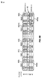
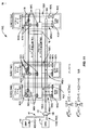
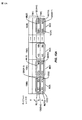
[00105]図8は、図7のプライマリタップ付き遅延線78(0)およびシャドウタップ付き遅延線78(1)の中に存在する選択されたプライマリパイプラインレジスタ120とシャドウパイプラインレジスタ122とを示す概略図である。図8は、プライマリパイプラインレジスタ120とシャドウパイプラインレジスタ122との間の入力ベクトルデータサンプル86のシフトの例を説明することを容易にするために提供される。上記で説明されたように、入力ベクトルデータサンプル86はまた、プライマリタップ付き遅延線78(0)およびシャドウタップ付き遅延線78(1)内で、ならびにシャドウタップ付き遅延線78(1)からプライマリタップ付き遅延線78(0)にシフトされ得る。パイプラインレジスタ120、122は、入力ベクトルデータサンプル86が必要な場合8ビットの解像度でシフトすることを可能にするために、この例では各々8ビット幅である。これは下記でより詳細に説明される。プライマリタップ付き遅延線78(0)およびシャドウタップ付き遅延線78(1)はまた、同様に下記でより詳細に説明されるように、入力ベクトルデータサンプル86の解像度の16ビットシフトと32ビットシフトとを実行することが可能である。
[00105] FIG. 8 shows selected primary pipeline registers 120 and shadow pipeline registers 122 present in primary tapped delay line 78 (0) and shadow tapped delay line 78 (1) of FIG. FIG. FIG. 8 is provided to facilitate describing an example of shifting input
[00106]この関連で、図8は、図7のプライマリタップ付き遅延線78(0)内に入力ベクトルデータサンプル86S(X)のための記憶レジスタを形成する、プライマリパイプラインレジスタ120(4X+3)、120(2X+1)、120(4X+2)、および120(2X)の中への入力ベクトルデータサンプル86のシフトを示す。プライマリパイプラインレジスタ120(4X+3)および120(4X+2)は、それぞれ、図7のプライマリタップ付き遅延線78(0)内のレジスタB31およびB30である。プライマリパイプラインレジスタ120(2X+1)および120(2X)は、それぞれ、図7のプライマリタップ付き遅延線78(0)内のレジスタA31およびA30である。図7に示されたように、レジスタB31およびB30のためのプライマリパイプラインレジスタ120(4X+3)および120(4X+2)は、シャドウタップ付き遅延線78(1)内の隣接するシャドウパイプラインレジスタ122からシフトされた入力ベクトルデータサンプル86を受信するように構成される。したがって、図8の例では、それぞれ、レジスタA’0およびA’1のためのシャドウパイプラインレジスタ122(0)および122(1)は、B31およびB30のためのプライマリパイプラインレジスタ120(4X+3)および120(4X+2)の中に入力ベクトルデータサンプル86をシフトするように構成されるものとして示される。同様に、図8の例では、プライマリタップ付き遅延線78(0)内の、それぞれ、レジスタB1およびB0のためのプライマリパイプラインレジスタ120(2X+3)および120(2X+2)は、レジスタA31およびA30のための隣接するプライマリパイプラインレジスタ120(2X+1)および120(2X)の中に入力ベクトルデータサンプル86をシフトするように構成されるものとして示される。これらのレジスタ間の入力ベクトルデータサンプル86の例示的なシフトが次に記載される。
[00106] In this regard, FIG. 8 illustrates a primary pipeline register 120 (4X + 3) that forms a storage register for input
[00107]引き続き図8を参照すると、図4ならびに入力ベクトルデータサンプル86のシフトにおいて、ベクトルデータファイル82(0)〜82(X)から新しい入力ベクトルデータサンプルセット86(0)〜86(X)をロードするように、プライマリパイプラインレジスタ120とシャドウパイプラインレジスタ122とを構成する柔軟性を提供するために、入力ベクトルデータサンプル選択器がプライマリパイプラインレジスタ120およびシャドウパイプラインレジスタ122の各々に関連付けられる。この関連で、プライマリタップ付き遅延線78(0)において、それぞれ、プライマリパイプラインレジスタ120(0)〜120(4X+3)の中にロードまたはシフトされるベクトルデータに、入力ベクトルデータサンプル選択器124(0)〜124(4X+3)が提供される。シャドウタップ付き遅延線78(1)において、それぞれ、シャドウパイプラインレジスタ122(0)〜122(4X+3)の中にロードまたはシフトされるベクトルデータに、入力ベクトルデータサンプル選択器126(0)〜126(4X+3)が提供される。入力ベクトルデータサンプル選択器124(0)〜124(4X+3)および入力ベクトルデータサンプル選択器126(0)〜126(4X+3)は、この例では各々マルチプレクサである。下記でより詳細に説明されるように、入力ベクトルデータサンプル選択器124(0)〜124(4X+3)、126(0)〜126(4X+3)は、各々、プライマリパイプラインレジスタ120(0)〜120(4X+3)およびシャドウパイプラインレジスタ122(0)〜122(4X+3)の中にロードまたはシフトされるべき入力ベクトルデータを選択するために、データ幅シフト制御入力125によって制御され得る。
[00107] With continued reference to FIG. 8, in the shift of FIG. 4 and the input
[00108]図8では、それぞれ、レジスタB31、B30、A31、およびA30に対応する、それぞれ、プライマリパイプラインレジスタ120(4X+3)、120(4X+2)、120(2X+1)、120(2X)のために、入力ベクトルデータサンプル選択器124(4X+3)、124(4X+2)、124(2X+1)、124(2X)のみが示されていることに留意されたい。図8では、それぞれ、レジスタA’1、A’0、B1、およびB0に対応する、それぞれ、パイプラインレジスタ122(1)、122(0)、120(2X+3)、120(2X+2)のために、入力ベクトルデータサンプル選択器126(1)、126(0)、124(2X+3)、124(2X+2)のみが示されている。 [00108] In Figure 8, respectively, corresponding to the register B 31, B 30, A 31 , and A 30, respectively, the primary pipeline register 120 (4X + 3), 120 (4X + 2), 120 (2X + 1), 120 (2X Note that only the input vector data sample selectors 124 (4X + 3), 124 (4X + 2), 124 (2X + 1), 124 (2X) are shown. In FIG. 8, for pipeline registers 122 (1), 122 (0), 120 (2X + 3), 120 (2X + 2) respectively corresponding to registers A ′ 1 , A ′ 0 , B 1 , and B 0 . Thus, only the input vector data sample selectors 126 (1), 126 (0), 124 (2X + 3), 124 (2X + 2) are shown.
[00109]引き続き図8を参照すると、ベクトル処理動作のために、新しい入力ベクトルデータがプライマリタップ付き遅延線78(0)およびシャドウタップ付き遅延線78(1)の中にロードされるべき場合、データ幅シフト制御入力125は、入力ベクトルデータサンプル選択器124(4X+3)、124(4X+2)、124(2X+1)、124(2X)に、ロードデータフローパス133(4X+3)、133(4X+2)、133(2X+1)、133(2X)を選択させるように、図4のVPE22(1)によって構成され得る。ロードデータフローパス133(4X+3)、133(4X+2)、133(2X+1)、133(2X)を選択すると、ベクトルデータファイル82(0)〜82(X)からの入力ベクトルデータがプライマリパイプラインレジスタ120(4X+3)、120(4X+2)、120(2X+1)、120(2X)に記憶されることが可能になる。ベクトルデータファイル82(0)〜82(X)から入力ベクトルデータをロードすることは、例としてVPE22(1)によって処理されるべき新しいまたは次のベクトル命令上で実行される場合がある。同様に、データ幅シフト制御入力125はまた、入力ベクトルデータサンプル選択器126(1)、124(2X+3)、126(0)、124(2X+2)に、入力データフローパス135(1)、133(2X+3)、135(0)、133(2X+2)を選択させるように、図4のVPE22(1)によって構成され得る。ロードデータフローパス135(1)、133(2X+3)、135(0)、133(2X+2)を選択すると、ベクトルデータファイル82(0)〜82(X)からの入力ベクトルデータがパイプラインレジスタ122(1)、120(2X+3)、124(0)、120(2X+2)に記憶されることが可能になる。
[00109] Referring still to FIG. 8, for vector processing operations, if new input vector data is to be loaded into the primary tapped delay line 78 (0) and the shadow tapped delay line 78 (1), The data width
[00110]引き続き図8を参照すると、ベクトル処理動作のために、プライマリタップ付き遅延線78(0)およびシャドウタップ付き遅延線78(1)に記憶されたベクトルデータがシフトされる必要がある場合、データ幅シフト制御入力125は、入力ベクトルデータサンプル選択器124(4X+3)、124(4X+2)、124(2X+1)、124(2X)に、ベクトルデータサンプルのシフトのための入力データフローパス137(4X+3)、137(4X+2)、137(2X+1)、137(2X)を選択させるように、図4のVPE22(1)によって構成され得る。データ幅シフト制御入力125はまた、入力ベクトルデータサンプル選択器126(1)、124(2X+3)、126(0)、124(2X+2)に、ベクトルデータサンプルのシフトのための入力データフローパス139(1)、137(2X+3)、139(0)、137(2X+2)を選択させる。そこに示されているように、入力ベクトルデータサンプル選択器124(4X+3)、124(4X+2)、124(2X+1)、124(2X)および入力ベクトルデータサンプル選択器126(1)、124(2X+3)、126(0)、124(2X+2)は、各々、ベクトルデータが他のレジスタにシフトされることを可能にする、それぞれ、出力データフローパス141(4X+3)、141(4X+2)、141(2X+1)、141(2X)および143(1)、141(2X+3)、143(0)、124(2X+2)を含む。図8に示された出力データフローパスは、次に全体が示される出力データフローパス141(0)〜141(4X+3)および143(0)〜143(4X+3)の一部であるが、それぞれ、プライマリタップ付き遅延線78(0)内の入力ベクトルデータサンプル選択器124(0)〜124(4X+3)およびシャドウタップ付き遅延線78(1)内の入力ベクトルデータサンプル選択器126(0)〜126(4X+3)のために含まれる。
[00110] Continuing with FIG. 8, when the vector data stored in the primary tapped delay line 78 (0) and the shadow tapped delay line 78 (1) needs to be shifted for vector processing operations. , The data width
[00111]例として、8ビットベクトルデータのシフト中、入力ベクトルデータサンプル選択器124(4X+3)、124(4X+2)、124(2X+1)、124(2X)および入力ベクトルデータサンプル選択器126(1)、124(2X+3)、126(0)、124(2X+2)は、それぞれ、入力データフローパス137(4X+3)、137(4X+2)、137(2X+1)、137(2X)、139(1)、137(2X+3)、139(0)、137(2X+2)を選択するように構成される。この関連で、例として、プライマリパイプラインレジスタ120(2X+1)(すなわち、A31)内のベクトルデータは、図8に示されたように、プライマリパイプラインレジスタ120(2X)(すなわち、A30)に出力データフローパス141(2X+1)上でシフトされる。プライマリパイプラインレジスタ120(4X+3)(すなわち、B31)内のベクトルデータは、図8に示されたように、プライマリパイプラインレジスタ120(4X+2)(すなわち、B30)に出力データフローパス141(4X+3)上でシフトされる。シャドウパイプラインレジスタ122(0)(すなわち、A’0)内のベクトルデータは、図8に示されたように、プライマリパイプラインレジスタ120(4X+3)(すなわち、B31)に出力データフローパス143(0)上でシフトされる。プライマリパイプラインレジスタ120(2X+3)(すなわち、B1)内のベクトルデータは、図8に示されたように、プライマリパイプラインレジスタ120(4X+2)(すなわち、B30)に出力データフローパス141(2X+3)上でシフトされる。シャドウパイプラインレジスタ122(1)(すなわち、A’1)内のベクトルデータは、図8に示されたように、シャドウパイプラインレジスタ122(0)(すなわち、A’0)に出力データフローパス143(1)上でシフトされる。プライマリパイプラインレジスタ120(2X+2)(すなわち、B0)内のベクトルデータは、図8に示されたように、プライマリパイプラインレジスタ120(2X+1)(すなわち、A31)に出力データフローパス141(2X+2)上でシフトされる。 [00111] As an example, during the shifting of 8-bit vector data, input vector data sample selectors 124 (4X + 3), 124 (4X + 2), 124 (2X + 1), 124 (2X) and input vector data sample selector 126 (1) , 124 (2X + 3), 126 (0), 124 (2X + 2) are input data flow paths 137 (4X + 3), 137 (4X + 2), 137 (2X + 1), 137 (2X), 139 (1), 137 (2X + 3), respectively. ) 139 (0), 137 (2X + 2). In this connection, by way of example, the vector data in primary pipeline register 120 (2X + 1) (ie, A 31 ) is represented by primary pipeline register 120 (2X) (ie, A 30 ) as shown in FIG. Shifted on the output data flow path 141 (2X + 1). The vector data in primary pipeline register 120 (4X + 3) (ie, B 31 ) is output to primary pipeline register 120 (4X + 2) (ie, B 30 ) as shown in FIG. 8, and output data flow path 141 (4X + 3). ) Shifted on. The vector data in shadow pipeline register 122 (0) (ie, A ′ 0 ) is output to primary pipeline register 120 (4X + 3) (ie, B 31 ) as shown in FIG. 0) shifted up. The vector data in the primary pipeline register 120 (2X + 3) (ie, B 1 ) is output to the primary pipeline register 120 (4X + 2) (ie, B 30 ) as shown in FIG. 8 in the output data flow path 141 (2X + 3). ) Shifted on. Shadow pipeline register 122 (1) (i.e., A '1) vector data in, as shown in FIG. 8, the shadow pipeline register 122 (0) (i.e., A' 0) output to the data flow path 143 (1) Shifted up. The vector data in primary pipeline register 120 (2X + 2) (ie, B 0 ) is output to primary pipeline register 120 (2X + 1) (ie, A 31 ) as shown in FIG. ) Shifted on.
[00112]引き続き図8を参照すると、16ビットベクトルデータのシフト中、入力ベクトルデータサンプル選択器124(4X+3)、124(4X+2)、124(2X+1)、124(2X)および入力ベクトルデータサンプル選択器126(1)、124(2X+3)、126(0)、124(2X+2)は、それぞれ、入力データフローパス145(4X+3)、145(4X+2)、145(2X+1)、145(2X)、147(1)、145(2X+3)、147(0)、145(2X+2)を選択するように構成される。この関連で、例として、プライマリパイプラインレジスタ120(2X+2)(すなわち、B0)内のベクトルデータは、図8に示されたように、プライマリパイプラインレジスタ120(2X)(すなわち、A30)に出力データフローパス141(2X+2)上でシフトされる。シャドウパイプラインレジスタ122(0)(すなわち、A’0)内のベクトルデータは、図8に示されたように、プライマリパイプラインレジスタ120(4X+2)(すなわち、B30)に出力データフローパス143(0)上でシフトされる。プライマリパイプラインレジスタ120(2X+3)(すなわち、B1)内のベクトルデータは、図8に示されたように、プライマリパイプラインレジスタ120(2X+1)(すなわち、A31)に出力データフローパス141(2X+3)上でシフトされる。シャドウパイプラインレジスタ122(1)(すなわち、A’1)内のベクトルデータは、図8に示されたように、プライマリパイプラインレジスタ120(4X+3)(すなわち、B31)に出力データフローパス143(1)上でシフトされる。 [00112] Still referring to FIG. 8, during the shifting of 16-bit vector data, input vector data sample selectors 124 (4X + 3), 124 (4X + 2), 124 (2X + 1), 124 (2X) and input vector data sample selectors 126 (1), 124 (2X + 3), 126 (0), 124 (2X + 2) are input data flow paths 145 (4X + 3), 145 (4X + 2), 145 (2X + 1), 145 (2X), 147 (1), respectively. 145 (2X + 3), 147 (0), and 145 (2X + 2). In this context, by way of example, the vector data in primary pipeline register 120 (2X + 2) (ie, B 0 ) is represented by primary pipeline register 120 (2X) (ie, A 30 ) as shown in FIG. Shifted on the output data flow path 141 (2X + 2). The vector data in shadow pipeline register 122 (0) (ie, A ′ 0 ) is transferred to primary pipeline register 120 (4X + 2) (ie, B 30 ) as shown in FIG. 0) shifted up. The vector data in primary pipeline register 120 (2X + 3) (ie, B 1 ) is output to primary pipeline register 120 (2X + 1) (ie, A 31 ) as shown in FIG. 8, in output data flow path 141 (2X + 3). ) Shifted on. The vector data in the shadow pipeline register 122 (1) (ie, A ′ 1 ) is transferred to the primary pipeline register 120 (4X + 3) (ie, B 31 ) as shown in FIG. 1) Shifted up.
[00113]プライマリタップ付き遅延線78(0)およびシャドウタップ付き遅延線78(1)において32ビットベクトルデータのシフトが望ましい場合、プライマリパイプラインレジスタ120(0)〜120(4X+3)およびシャドウパイプラインレジスタ122(0)〜122(4X+3)に記憶されたベクトルデータは、必要な場合、2つの16ビットベクトルデータのシフト動作においてシフトされ得る。 [00113] When 32-bit vector data shift is desired in the primary tapped delay line 78 (0) and the shadow tapped delay line 78 (1), the primary pipeline registers 120 (0) -120 (4X + 3) and the shadow pipeline Vector data stored in registers 122 (0) -122 (4X + 3) can be shifted in a shift operation of two 16-bit vector data, if necessary.
[00114]図7では、レジスタB31およびB30のためのプライマリパイプラインレジスタ120(4X+3)および120(4X+2)、ならびにレジスタA31およびA30のためのプライマリパイプラインレジスタ120(2X+1)および120(2X)は、シフトされた入力ベクトルデータサンプル86S(X)に対して互いに論理的に関連付けられるが、図8に示されたように、互いに物理的に隣接していないことに留意されたい。この配置は、図6Bに示されたように、ベクトルデータファイル82(0)〜82(X)内の入力ベクトルデータサンプルセット86(0)〜86(X)の記憶パターンに起因して、この例において提供される。同様に図6Bに示されたように、ベクトルデータファイル82(0)〜82(X)に記憶された入力ベクトルデータサンプルセット86(0)〜86(X)は、ADDRESS0およびADDRESS1をまたぐ。しかしながら、本明細書内の開示は、ベクトルデータファイル82(0)〜82(X)内の入力ベクトルサンプルセット86(0)〜86(X)のこの記憶パターンに限定されないことに留意されたい。
[00114] In Figure 7, the
[00115]さらに、図8に関して、タップ付き遅延線78(0)、78(1)は、実行されるべきベクトル命令に従って、タップ付き遅延線78(0)、78(1)のためのプログラム可能な入力データパス構成に基づいて、ベクトルデータファイル82(0)〜82(X)と実行ユニット84(0)〜84(X)との間の入力データフローパス80(0)〜80(X)内に、選択的に設けられるか、または設けられないように構成可能である。たとえば、ベクトル命令がフィルタベクトル処理命令ではなく、および/または場合によっては入力ベクトルデータサンプルセット86(0)〜86(X)をシフトするためにタップ付き遅延線78(0)、78(1)を必要としない場合、タップ付き遅延線78(0)、78(1)は、入力ベクトルデータサンプルセット86(0)〜86(X)をラッチしないように構成され得る。入力ベクトルデータサンプルセット86(0)〜86(X)は、プライマリタップ付き遅延線78(0)とシャドウタップ付き遅延線78(1)とをバイパスすることによって、それぞれの実行ユニット84(0)〜84(X)にベクトルデータファイル82(0)〜82(X)から供給され得る。このプログラム可能なデータパス構成により、さらに、プライマリタップ付き遅延線78(0)およびシャドウタップ付き遅延線78(1)が入力データフローパス80(0)〜80(X)内に設けられるか、または設けられないことが可能になる。プライマリタップ付き遅延線78(0)およびシャドウタップ付き遅延線78(1)は、必要に応じて、ベクトル命令ごとに、入力データフローパス80(0)〜80(X)内に設けられるか、または設けられないようにプログラムされ得る。 [00115] Further, with respect to FIG. 8, tapped delay lines 78 (0), 78 (1) are programmable for tapped delay lines 78 (0), 78 (1) according to vector instructions to be executed. In the input data flow paths 80 (0) to 80 (X) between the vector data files 82 (0) to 82 (X) and the execution units 84 (0) to 84 (X) based on the various input data path configurations Can be configured to be selectively provided or not provided. For example, the vector instructions are not filter vector processing instructions and / or in some cases tapped delay lines 78 (0), 78 (1) to shift the input vector data sample sets 86 (0) -86 (X). Are not required, the tapped delay lines 78 (0), 78 (1) may be configured not to latch the input vector data sample sets 86 (0) -86 (X). The input vector data sample sets 86 (0) -86 (X) are bypassed from the primary tapped delay line 78 (0) and the shadow tapped delay line 78 (1), respectively, so that each execution unit 84 (0). To 84 (X) may be supplied from the vector data files 82 (0) to 82 (X). This programmable data path configuration further provides a primary tapped delay line 78 (0) and a shadow tapped delay line 78 (1) in the input data flow paths 80 (0) -80 (X), or It becomes possible not to be provided. Primary tapped delay line 78 (0) and shadow tapped delay line 78 (1) are provided in the input data flow paths 80 (0) -80 (X) for each vector instruction as required, or It can be programmed not to be provided.
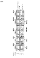
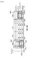
[00116]図9Aは、フィルタベクトル処理命令の第1のクロックサイクル(CYCLE0)の間にプライマリタップ付き遅延線78(0)の中にベクトルデータファイル82(0)〜82(X)からロードされた入力ベクトルデータサンプルセット86(0)〜86(X)を示す。プライマリタップ付き遅延線78(0)およびシャドウタップ付き遅延線78(1)は、図7から簡略化された形式で示されている。グローバルレジスタファイル40も示されている。最初の入力ベクトルデータサンプルセット86(0)〜86(X)が入力ベクトルデータサンプルX0〜X63としてプライマリタップ付き遅延線78(0)の中にロードされる。たとえば、プライマリタップ付き遅延線78(0)の中に(および下記でより詳細に説明されるように、シャドウタップ付き遅延線78(1)の中にも)最初の入力ベクトルデータサンプルセット86(0)〜86(X)をロードするために、特殊ベクトル命令がサポートされる場合がある。この最初の入力ベクトルデータサンプルセット86(0)〜86(X)は、図6Bに示されたように、ベクトルデータファイル82(0)〜82(X)内のADDRESS0およびADDRESS1に記憶された。ひとえにこの例のための図4のVPE22(1)内のベクトルデータファイル82(0)〜82(X)の記憶パターンのせいで、この例では、X0、X1、X32、およびX33が最初の入力ベクトルデータサンプル86(0)を形成することに留意されたい。他の入力ベクトルデータサンプル86は、同様に、図9Aに示されたように形成される(たとえば、86(1)、86(2)、...86(X))。入力ベクトルデータサンプル86を一緒にグループ化して、入力ベクトルデータサンプルセット86(0)〜86(X)を形成するために、他のパターンが提供される可能性がある。
[00116] FIG. 9A is loaded from the vector data files 82 (0) -82 (X) into the primary tapped delay line 78 (0) during the first clock cycle (CYCLE0) of the filter vector processing instruction. The input vector data sample sets 86 (0) to 86 (X) are shown. The primary tapped delay line 78 (0) and the shadow tapped delay line 78 (1) are shown in simplified form from FIG. A
[00117]図9Bは、フィルタベクトル処理命令の第2のクロックサイクル(CYCLE1)の間にシャドウタップ付き遅延線78(1)の中にロードされた次の入力ベクトルデータサンプルセット86N(0)〜86N(X)を示す。フィルタ処理動作の実行をセットアップするために、ベクトルデータファイル82(0)〜82(X)からの最初の入力ベクトルデータサンプルセット86(0)〜86(X)がプライマリタップ付き遅延線78(0)の中にロードされた後に、次の入力ベクトルデータサンプルセット86N(0)〜86N(X)がシャドウタップ付き遅延線78(1)の中にロードされる。この次の入力ベクトルデータサンプルセット86N(0)〜86N(X)は、入力ベクトルデータサンプルX64〜X127としてシャドウタップ付き遅延線78(1)の中にロードされる。この次の入力ベクトルデータサンプルセット86N(0)〜86N(X)は、図6Bに示されたように、ベクトルデータファイル82(0)〜82(X)内のADDRESS2およびADDRESS3に記憶された。ひとえにこの例のための図4のVPE22(1)内のベクトルデータファイル82(0)〜82(X)の記憶パターンのせいで、この例では、X64、X65、X96、およびX97が最初の入力ベクトルデータサンプル86(0)を形成することに留意されたい。入力ベクトルデータサンプル86を一緒にグループ化して、入力ベクトルデータサンプルセット86(0)〜86(X)を形成するために、他のパターンが提供される可能性がある。グローバルレジスタファイル40からの最初のフィルタ係数92(0)も、フィルタベクトル処理動作102において使用するために図9Bの実行ユニット84(0)〜84(X)へのレジスタ(「C」)内に設けられるものとして示される。
[00117] FIG. 9B shows the next input vector data sample set 86N (0)-loaded into the shadow tapped delay line 78 (1) during the second clock cycle (CYCLE1) of the filter vector processing instruction. 86N (X) is shown. To set up the execution of the filtering operation, the first input vector data sample set 86 (0) -86 (X) from the vector data files 82 (0) -82 (X) is represented by the primary tapped delay line 78 (0 ) Is loaded into the shadow tapped delay line 78 (1). The next input vector data sample set 86N (0) -86N (X) is loaded. This next input vector data sample set 86N (0) -86N (X) is loaded into the delay line 78 (1) with shadow tap as input vector data samples X64-X127. This next input vector data sample set 86N (0) -86N (X) was stored in ADDRESS2 and ADDRESS3 in vector data files 82 (0) -82 (X) as shown in FIG. 6B. Due to the storage pattern of vector data files 82 (0) -82 (X) in VPE 22 (1) of FIG. 4 for this example, in this example, X64, X65, X96, and X97 are the first inputs. Note that the vector data sample 86 (0) is formed. Other patterns may be provided to group input
[00118]図7に戻って参照すると、フィルタベクトル処理動作102の各処理ステージの間に入力ベクトルデータサンプル86がプライマリタップ付き遅延線78(0)内でシフトされるとき、シャドウパイプラインレジスタ122に記憶された次の入力ベクトルデータサンプル86Nも、シャドウタップ付き遅延線78(1)のシャドウパイプラインレジスタ122内でシフトされる。図7の最初のシャドウパイプラインレジスタ122(0)に記憶された入力ベクトルデータサンプル86は、各シフトの間にプライマリタップ付き遅延線78(0)の最後のプライマリパイプラインレジスタ120(4X+3)の中にシフトされる。したがって、このようにして、フィルタベクトル処理動作102の処理ステージが実行ユニット84(0)〜84(X)において進行するとき、シャドウタップ付き遅延線78(1)に最初に記憶された次の入力ベクトルデータサンプルセット86N(0)〜86N(X)の少なくとも一部分は、処理のために実行ユニット84(0)〜84(X)に供給されるために、プライマリタップ付き遅延線78(0)の中にシフトされる。シフトの回数は、この例ではフィルタベクトル処理動作102において提供されたフィルタタップの数に依存する。ベクトルデータファイル82(0)〜82(X)からプライマリタップ付き遅延線78(0)およびシャドウタップ付き遅延線78(1)の中にフェッチされた入力ベクトルデータサンプルセット86(0)〜86(X)内の入力ベクトルデータサンプル86の数が、フィルタベクトル処理動作102におけるフィルタタップの数よりも大きい場合、実行ユニット84(0)〜84(X)は、任意のさらなる入力ベクトルデータサンプルセット86(0)〜86(X)がベクトルデータファイル82(0)〜82(X)から再フェッチされることなく、フィルタベクトル処理動作102を実行することができる。しかしながら、フィルタベクトル処理動作102におけるフィルタタップの数が、ベクトルデータファイル82(0)〜82(X)からプライマリタップ付き遅延線78(0)およびシャドウタップ付き遅延線78(1)の中にフェッチされた入力ベクトルデータサンプルセット86(0)〜86(X)内の入力ベクトルデータサンプル86よりも大きい場合、フィルタベクトル処理動作102の一部として、さらなる入力ベクトルデータサンプルセット86(0)〜86(X)がベクトルデータファイル82(0)〜82(X)からフェッチされ得る。フィルタベクトル処理動作102がシフトされた入力ベクトルデータサンプルセット86S(0)〜86S(X)に対して完了した後、タップ付き遅延線78(0)、78(1)内に未処理の入力ベクトルデータサンプル86Sが存在する場合、実行ユニット84(0)〜84(X)は、次いで、次のフィルタベクトル処理動作のためのシフトされた入力ベクトルデータサンプルセット86S(0)〜86S(X)として、プライマリタップ付き遅延線78(0)に記憶された前の次の入力ベクトルデータサンプルセット86N(0)〜86N(X)を供給され得る。
[00118] Referring back to FIG. 7, when the input
[00119]シャドウタップ付き遅延線78(1)を提供するための別の例示的な論理的根拠は以下の通りである。現在のフィルタベクトル処理動作102が、ベクトルデータレーン100(0)〜100(X)の幅で提供され得るよりも多くの入力ベクトルデータサンプル86を要する場合、シャドウタップ付き遅延線78(1)の中にロードされたさらなる入力ベクトルデータサンプルセット86(0)〜86(X)は、遅延がないフィルタベクトル処理動作102の間、実行ユニット84(0)〜84(X)に利用可能である。フィルタベクトル処理動作102が、実行中シフトされた入力ベクトルデータサンプルセット86S(0)〜86S(X)を通じて進行するとき、上記で説明されたように、シャドウタップ付き遅延線78(1)の中にロードされたさらなる次の入力ベクトルデータサンプルセット86N(0)〜86N(X)が、プライマリタップ付き遅延線78(0)の中にシフトされる。したがって、このようにして、実行ユニット84(0)〜84(X)によるベクトル処理において使用するための次の入力ベクトルデータサンプルセット86N(0)〜86N(X)は、遅延なく利用可能である。ベクトルデータファイル82(0)〜82(X)の幅の単一のフェッチされた入力ベクトルデータサンプルセット86(0)〜86(X)が、フィルタベクトル処理動作102全体を実行するのに十分であるかどうかにかかわらず、実行ユニット84(0)〜84(X)は、フィルタベクトル処理動作102の間、十分に利用され続けることができる。
[00119] Another exemplary rationale for providing a shadow tapped delay line 78 (1) is as follows. If the current filter
[00120]最初の入力ベクトルデータサンプルセット86N(0)〜86N(X)および次の入力ベクトルデータサンプルセット86N(0)〜86N(X)が、それぞれ、プライマリタップ付き遅延線78(0)およびシャドウタップ付き遅延線78(1)の中にロードされた後、プライマリタップ付き遅延線78(0)に供給された最初の入力ベクトルデータサンプルセット86(0)〜86(X)は、フィルタベクトル処理動作102の最初の処理ステージにおいて処理されるために、それぞれの実行ユニット84(0)〜84(X)に供給される(図5のブロック108)。最初の入力ベクトルデータサンプルセット86(0)〜86(X)が実行ユニット84(0)〜84(X)によって処理された後、最初の入力ベクトルデータサンプルセット86(0)〜86(X)は、実行ユニット84(0)〜84(X)によって処理されるべきシフトされた入力ベクトルデータサンプルセット86S(0)〜86S(X)になるために、プライマリタップ付き遅延線78(0)内でシフトされる。図4のVPE22(1)において示されたように、シフトされた入力ベクトルデータサンプル86S(0)は実行ユニット84(0)に供給され、シフトされた入力ベクトルデータサンプル86S(1)は実行ユニット84(1)に供給され、以下同様である。
[00120] The first input vector data sample set 86N (0) -86N (X) and the next input vector data sample set 86N (0) -86N (X) are respectively connected to the primary tapped delay line 78 (0) and After loading into the shadow tapped delay line 78 (1), the first input vector data sample set 86 (0) -86 (X) supplied to the primary tapped delay line 78 (0) is the filter vector. To be processed in the first processing stage of
[00121]次に、実行ユニット84(0)〜84(X)は、フィルタベクトル処理動作102を実行する(図5のブロック110)。より詳細には、実行ユニット84(0)〜84(X)は、この例では演算:y[n]=x[n−7]*h7に従って、第1の繰返しにおいて最初の入力ベクトルデータサンプルセット86(0)〜86(X)を現在のフィルタ係数92(0)と乗算し、ここで、x[n−7]は、結果として生じるフィルタ出力ベクトルデータサンプルセット94(0)〜94(X)を供給する最初の入力ベクトルデータサンプルセット86(0)〜86(X)である。フィルタベクトル処理動作102の次の繰返し(図5のブロック110)において、フィルタベクトル処理動作102のための次のシフトされた入力ベクトルデータサンプルセット86S(0)〜86S(X)は、現在のフィルタ係数92(1)〜92(Y−1)と乗算される。実行ユニット84(0)〜84(X)は、新しい前の、結果として生じるフィルタ出力ベクトルデータサンプルセット94(0)〜94(X)を供給するために、結果として生じるフィルタ出力ベクトルデータサンプルセット94(0)〜94(X)を、実行ユニット84(0)〜84(X)によって計算された前の、結果として生じるフィルタ出力ベクトルデータサンプルセット94(0)〜94(X)と累算する(図5のブロック112)。フィルタベクトル処理動作102の最初の処理ステージでは、前の、結果として生じるフィルタ出力ベクトルデータサンプルセットは存在しない。
[00121] Next, execution units 84 (0) -84 (X) perform a filter vector processing operation 102 (block 110 of FIG. 5). More specifically, execution units 84 (0) -84 (X), in this example, follow the operation: y [n] = x [n−7] * h7, the first set of input vector data samples in the first iteration. 86 (0) -86 (X) is multiplied by the current filter coefficient 92 (0), where x [n-7] is the resulting filter output vector data sample set 94 (0) -94 (X ) Is the first input vector data sample set 86 (0) -86 (X). In the next iteration of the filter vector processing operation 102 (block 110 of FIG. 5), the next shifted input vector data sample sets 86S (0) -86S (X) for the filter
[00122]フィルタベクトル処理動作102のすべての処理ステージが完了した場合(図5のブロック114)、ベクトルデータファイル82(0)〜82(X)に供給され記憶されるために、出力データフローパス98(0)〜98(X)内の、結果として生じるフィルタ出力ベクトルデータサンプルセット94(0)〜94(X)として、累算された前の、結果として生じるフィルタ出力ベクトルデータサンプルセット94(0)〜94(X)が供給される(図5のブロック116)。フィルタベクトル処理動作102のすべての処理ステージが完了していない場合(図5のブロック114)、フィルタベクトル処理動作102に次のシフトされた入力ベクトルデータサンプルセット86S(0)〜86S(X)を供給するために、タップ付き遅延線78(0)および78(1)に記憶されたサンプルがタップ付き遅延線78(0)、78(1)内でシフトされる(図5のブロック118)。シフトされた入力ベクトルデータサンプルセット86S(0)〜86S(X)は、フィルタベクトル処理動作102が完了するまで、前の、結果として生じるフィルタ出力ベクトルデータサンプルセットと累算されるために、中間結果として次の、結果として生じるフィルタ出力ベクトルデータサンプルセットを計算するために供給される。タップ付き遅延線78(0)、78(1)内にシフトされた入力ベクトルデータサンプルセット86S(0)〜86S(X)を供給するために入力ベクトルデータサンプル86をシフトすることは、図7に関して詳細に上記で前述された。フィルタベクトル処理動作102に実行ユニット84(0)〜84(X)によって供給された中間結果の最終的な累算は、図4に示されたように、実行ユニット84(0)〜84(X)から、結果として生じるフィルタ出力ベクトルデータサンプルセット94(0)〜94(X)として供給される。
[00122] When all processing stages of the filter
[00123]図9Cは、次のフィルタ処理動作y[n]=x[n−6]*h6のための次のシフトされた入力ベクトルデータサンプルセット86S(0)〜86S(X)になるために、フィルタベクトル処理動作102の2番目の処理ステージにおいて、入力ベクトルデータサンプルセット86(0)〜86(X)がシフトされたときのタップ付き遅延線78のコンテンツを示す。プライマリタップ付き遅延線78(0)内のシフトされた入力ベクトルデータサンプルセット86S(0)〜86S(X)は、実行されているベクトル命令によって規定された入力ベクトルデータサンプルのシフト幅に従って、プライマリパイプラインレジスタ120(0)〜120(4X+3)内でシフトされる。たとえば、図9Cに示されたように、サンプルX2はシフトされた入力ベクトルデータサンプル86S(0)内でシフトされる。新しいシフトされた入力ベクトルデータサンプルセット86S(0)〜86S(X)は、フィルタベクトル処理動作102の次のフィルタタップのための実行のために、実行ユニット84(0)〜84(X)に供給される。実行ユニット84(0)〜84(X)に供給されたフィルタ係数92は、この例では「h6」である次のフィルタ係数92でもある。
[00123] FIG. 9C is the next shifted input vector data sample set 86S (0) -86S (X) for the next filtering operation y [n] = x [n-6] * h6. 6 shows the contents of the tapped
[00124]引き続き図5を参照すると、次のフィルタ係数92と乗算される(図5のブロック110)ために、実行ユニット84(0)〜84(X)にプライマリタップ付き遅延線78(0)からシフトされた入力ベクトルデータサンプルセット86S(0)〜86S(X)を供給する(図5のブロック108)ことによって、プロセスは繰り返す。結果として生じるフィルタ出力ベクトルデータサンプルセット94(0)〜94(X)が前の、結果として生じるフィルタ出力ベクトルデータサンプルセット94(0)〜94(X)と累算される(図5のブロック112)。図9Dは、例示的なフィルタベクトル処理動作102の最後の処理ステージの間、タップ付き遅延線78(0)、78(1)内に存在する入力ベクトルデータサンプル86の状態を示す。図9Dに示されたこの例では、フィルタ係数92「h7」〜「h0」(すなわち、92(0)〜92(Y−1))のせいで、フィルタベクトル処理動作102において8個のフィルタタップ(Y)が存在した。図9Dに示されたように、「h0」はフィルタベクトル処理動作102における最後のフィルタ係数92である。シフトされた入力ベクトルデータサンプルセット86S(0)〜86S(X)は(フィルタタップの数よりも1回少ない)7回シフトされており、その結果、フィルタベクトル処理動作102のための最後の8番目の処理ステージにおいて、入力ベクトルデータサンプルX39がプライマリタップ付き遅延線78(0)内のシフトされた入力ベクトルデータサンプル86S(0)に記憶される。
[00124] With continued reference to FIG. 5, the primary tapped delay line 78 (0) in the execution units 84 (0) -84 (X) to be multiplied by the next filter coefficient 92 (block 110 of FIG. 5). The process repeats by providing input vector data sample sets 86S (0) -86S (X) shifted from (block 108 in FIG. 5). The resulting filter output vector data sample sets 94 (0) -94 (X) are accumulated with the previous resulting filter output vector data sample sets 94 (0) -94 (X) (block of FIG. 5). 112). FIG. 9D shows the state of the input
[00125]上述されたフィルタベクトル処理動作102の例は、フィルタベクトル処理動作102を提供するためにVPE22(1)内のベクトルデータレーン100(0)〜100(X)の各々を利用するが、それは必要でないことに留意されたい。フィルタベクトル処理動作102は、フィルタベクトル処理動作102に利用されるべきベクトルデータレーン100(0)〜100(X)のサブセットを必要とするにすぎない場合がある。たとえば、入力ベクトルデータサンプルセット86(0)〜86(X)の幅がすべてのベクトルデータファイル82(0)〜82(X)の幅よりも小さい場合があり、ここで、フィルタベクトル処理動作102と並列に実行されるべき他のベクトル処理動作にさらなるベクトルデータレーン100を利用することが望ましい。このシナリオでは、図7のタップ付き遅延線78(0)、78(1)は、最後のベクトルデータレーン100(X)に到達するより前に、ベクトルデータレーン100内のシフトされた入力ベクトルデータサンプルセット86S(0)〜86S(X)として、シャドウタップ付き遅延線78(1)からプライマリタップ付き遅延線78(0)に次の入力ベクトルデータサンプルセット86N(0)〜86N(X)をシフトするように、修正される必要があり得る。
[00125] The example of the filter
[00126]図10は、上記の例における例示的な8個のタップフィルタベクトル処理ステージが、y[n]=x[n]*h0+x[n−1]*h1+...+x[n−7]*h7に従って完全に実行された後の、図4のVPE22(1)内の実行ユニット84(0)〜84(X)内の累算器のコンテンツ(すなわち、結果として生じるフィルタ出力ベクトルデータサンプル94)の概略図である。この例では、各実行ユニット84(0)〜84(X)は、ベクトルデータレーン100(0)〜100(X)ごとに並列に配置された4つの累算器を有するので、累算器Acc0〜Acc3が図10に示されている。累算された、結果として生じる出力ベクトルデータサンプルは、さらなる分析および/または処理のためにそこに記憶されるべき全体の、結果として生じるフィルタ出力ベクトルデータサンプルセット94(0)〜94(X)として、ベクトルデータファイル82(0)〜82(X)に出力データフローパス98(0)〜98(X)上で供給され得る。必要な場合、ベクトルデータファイル82(0)〜82(X)から図2のベクトルユニットデータメモリ32に、結果として生じるフィルタ出力ベクトルデータサンプルセット94(0)〜94(X)の行を移動するために、特殊なベクトル命令がVPE22(1)によってサポートされる場合がある。
[00126] FIG. 10 illustrates that the exemplary eight tap filter vector processing stages in the above example are y [n] = x [n] * h0 + x [n-1] * h1 +. . . The contents of the accumulators in execution units 84 (0) -84 (X) in VPE 22 (1) of FIG. 4 after complete execution according to + x [n-7] * h7 (ie, the resulting FIG. 6 is a schematic diagram of a filter output vector data sample 94). In this example, each execution unit 84 (0) -84 (X) has four accumulators arranged in parallel for each of the vector data lanes 100 (0) -100 (X), so the accumulator Acc0 ~ Acc3 is shown in FIG. The accumulated resulting output vector data samples are then stored in the entire resulting filtered output vector data sample set 94 (0) -94 (X) to be stored for further analysis and / or processing. As such, vector data files 82 (0) -82 (X) may be supplied on output data flow paths 98 (0) -98 (X). If necessary, move the resulting row of filter output vector data sample sets 94 (0) -94 (X) from the vector data files 82 (0) -82 (X) to the vector
[00127]フィルタベクトル処理動作102以外の他のタイプのベクトル処理動作も、上記で説明された図4のVPE22(1)内に設けられたタップ付き遅延線78と同じまたは同様のタップ付き遅延線78の使用による、VPEにおける処理効率を享受することができる。たとえば、VPEにおける入力ベクトルデータサンプルセット86のシフトを伴う別の特殊なベクトル処理動作は、(本明細書では「相関ベクトル処理動作」と呼ばれる)相関/共分散ベクトル処理動作である。例として、CDMAシステムにおいてユーザ信号と他のユーザの信号との間の良好な分離を提供するために、CDMAシステムにおいてユーザ信号を復調するための直接スペクトル拡散コード(DSSC)(すなわち、チップシーケンス)を選ぶために相関演算を提供するようにベクトル処理を利用することが望ましい場合がある。信号の分離は、受信された信号を所望のユーザのローカルに生成されたチップシーケンスと相関させることによって行われる。信号が所望のユーザのチップシーケンスと一致する場合、相関関数は高くなり、CDMAシステムはその信号を抽出することができる。所望のユーザのチップシーケンスが信号と共通する部分を少ししか、またはまったく有していない場合、相関は可能な限りゼロに近い(したがって信号を除去する)はずであり、これは相互相関と呼ばれる。チップシーケンスがゼロ以外の任意の時間オフセットで信号と相関される場合、相関は可能な限りゼロに近いはずである。これは自己相関と呼ばれ、マルチパス干渉を拒絶するために使用される。
[00127] Other types of vector processing operations other than the filter
[00128]しかしながら、相関演算は、ベクトルプロセッサにおいて提供される特殊なデータフローパスに起因して、ベクトルプロセッサにおいて並列化することは困難であり得る。相関されるべき信号を表す入力ベクトルデータサンプルセットが遅延タップ間でシフトされると、入力ベクトルデータサンプルセットはベクトルデータファイルから再フェッチされ、したがって電力消費が増大し、スループットが低減される。メモリからの入力ベクトルデータサンプルセットの再フェッチを最小化するために、データフローパスは、効率的な並列化処理のために、遅延タップと同じ数の乗算器を設けるように構成される可能性がある。しかしながら、他のベクトル処理動作は、より少ない乗算器しか必要としない場合があり、それにより、データフローパス内の乗算器の非効率的なスケーリングおよび過少利用がもたらされる。スケーラビリティを提供するために、乗算器の数が遅延タップの数よりも少なくなるように削減された場合、相関処理の様々なフェーズに対して同じ入力ベクトルデータサンプルセットを取得するために、メモリにより多くの再フェッチが必要とされることによって、並列化が制限される。 [00128] However, correlation operations may be difficult to parallelize in a vector processor due to the special data flow path provided in the vector processor. When the input vector data sample set representing the signal to be correlated is shifted between delay taps, the input vector data sample set is refetched from the vector data file, thus increasing power consumption and reducing throughput. In order to minimize refetching of input vector data sample sets from memory, the data flow path may be configured to provide as many multipliers as delay taps for efficient parallel processing. is there. However, other vector processing operations may require fewer multipliers, leading to inefficient scaling and underutilization of the multipliers in the data flow path. In order to provide scalability, if the number of multipliers is reduced to be less than the number of delay taps, the memory can be used to obtain the same set of input vector data samples for the various phases of the correlation process. The need for many refetches limits parallelism.
[00129]この関連で、図11は、図2のVPE22として提供され得る別の例示的なVPE22(2)の概略図である。下記でより詳細に記載されるように、図11のVPE22(2)は、ベクトルデータサンプルの再フェッチが除去または低減され、電力消費が低減される、VPE22(2)内の精度相関ベクトル処理動作を提供するように構成される。精度相関ベクトル処理動作は、ベクトルデータサンプルの再フェッチを必要とし、それにより結果として電力消費が増大する、中間結果の記憶を必要とする相関ベクトル処理動作と比較して、VPE22(2)において提供され得る。ベクトルデータファイルからの入力ベクトルデータサンプルの再フェッチを除去または最小化して、電力消費を低減し、処理効率を改善するために、図4のVPE22(1)に含まれるタップ付き遅延線78も、VPE22(2)内のベクトルデータファイル82(0)〜82(X)と(「EU」とも標記される)実行ユニット84(0)〜84(X)との間の入力データフローパス80(0)〜80(X)に含まれる。「X」+1は、この例におけるベクトルデータサンプルの処理用にVPE22(2)内に設けられる並列入力データレーンの最大数である。上記で前に説明されたように、タップ付き遅延線78は、ベクトルデータファイル82(0)〜82(X)の対応するサブセットまたはすべてから入力ベクトルデータサンプルセット86(0)〜86(X)の入力ベクトルデータサンプル86のサブセットまたはすべてとして、タップ付き遅延線入力88(0)〜88(X)上で入力ベクトルデータサンプルセット86(0)〜86(X)を受信するように構成される。すべての入力ベクトルデータサンプル86は、入力ベクトルデータサンプルセット86(0)〜86(X)を備える。下記でより詳細に説明されるように、ベクトルデータファイル82(0)〜82(X)からの入力ベクトルデータサンプルセット86(0)〜86(X)は、結果として生じる相関出力ベクトルデータサンプルセット132(0)〜132(X)を供給するために、基準ベクトルデータサンプルセット130(0)〜130(X)とVPE22(2)において相関される。基準ベクトルデータサンプルセット130(0)〜130(X)は、この例では130(0)、130(1)、...、および130(X)である、「X+1」個の基準ベクトルデータサンプル130から構成される。結果として生じる相関出力ベクトルデータサンプルセット132(0)〜132(X)は、この例では132(0)、132(1)、...、および132(X)である、「X+1」個の、結果として生じる相関出力ベクトルデータサンプル132から構成される。
[00129] In this regard, FIG. 11 is a schematic diagram of another exemplary VPE 22 (2) that may be provided as the
[00130]引き続き図11を参照すると、タップ付き遅延線78は、シフトされた入力ベクトルデータサンプルセット86S(0)〜86S(X)を供給するために、VPE22(2)によって実行されるべき相関ベクトル命令に従う相関ベクトル処理動作の相関遅延タップ(すなわち、相関処理ステージ)ごとに、入力ベクトルデータサンプルセット86(0)〜86(X)をシフトする。シフトされた入力ベクトルデータサンプル86Sのすべては、シフトされた入力ベクトルデータサンプルセット86S(0)〜86S(X)を備える。タップ付き遅延線78は、相関ベクトル処理動作中、実行ユニット84(0)〜84(X)の実行ユニット入力90(0)〜90(X)にシフトされた入力ベクトルデータサンプルセット86S(0)〜86S(X)を供給するために、入力ベクトルデータサンプルセット86(0)〜86(X)をシフトする。このようにして、シフトされた入力ベクトルデータサンプルセット86S(0)〜86S(X)に対して実行される動作に基づく中間相関結果は、VPE22(2)によって実行される相関ベクトル処理動作の各処理ステージの間に、記憶、シフト、およびベクトルデータファイル82(0)〜82(X)から再フェッチされる必要がない。このように、タップ付き遅延線78は、電力消費を低減し、VPE22(2)によって実行される相関ベクトル処理動作についての処理効率を上げることができる。
[00130] With continued reference to FIG. 11, the tapped
[00131]引き続き図11を参照すると、実行ユニット84(0)〜84(X)は、相関ベクトル処理動作のためのシーケンス番号発生器(SNG)134に記憶された基準ベクトルデータサンプルセット130(0)〜130(X)の中から基準ベクトルデータサンプル130も受信する。実行ユニット84(0)〜84(X)は、相関ベクトル処理動作の一部として、基準ベクトルデータサンプルセット130(0)〜130(X)を入力ベクトルデータサンプルセット86(0)〜86(X)と相関させるように構成される。しかしながら、シーケンス番号発生器(SNG)134はレジスタまたは他のファイルでもあり得ることに留意されたい。この例における相関ベクトル処理動作はCDMA相関ベクトル命令向けなので、シーケンス番号発生器134は、基準ベクトルデータサンプルセット130(0)〜130(X)を供給するために、この実施形態において提供される。基準ベクトルデータサンプルセット130(0)〜130(X)と入力ベクトルデータサンプルセット86(0)〜86(X)との間の相関が高い場合、基準ベクトルデータサンプルセット130(0)〜130(X)は、入力ベクトルデータサンプルセット86(0)〜86(X)からの信号抽出に使用するための生成されたチップシーケンスとして供給される。
[00131] With continued reference to FIG. 11, the execution units 84 (0) -84 (X) have the reference vector data sample set 130 (0) stored in the sequence number generator (SNG) 134 for correlation vector processing operations. ) To 130 (X), the reference
[00132]たとえば、CDMAベクトル相関命令向けの相関ベクトル処理動作は、入力ベクトルデータサンプルセット86(0)〜86(X)内のオンタイム入力ベクトルデータサンプル86と、入力ベクトルデータサンプルセット86(0)〜86(X)内の後発入力ベクトルデータサンプルとの間の相関を提供する可能性がある。たとえば、入力ベクトルデータサンプルセット86(0)〜86(X)内のオンタイム入力ベクトルデータサンプル86は、入力ベクトルデータサンプルセット86(0)〜86(X)内の偶数の入力ベクトルデータサンプル86(たとえば、86(0)、86(2)、86(4)、...86(X−1))であり得る。入力ベクトルデータサンプルセット86(0)〜86(X)内の後発入力ベクトルデータサンプル86は、入力ベクトルデータサンプルセット86(0)〜86(X)内の奇数の入力ベクトルデータサンプル86(たとえば、86(1)、86(3)、86(5)、...86(X))であり得る。代替として、オンタイム入力ベクトルデータサンプル86は奇数の入力ベクトルデータサンプル86であり得るし、後発入力ベクトルデータサンプル86は偶数の入力ベクトルデータサンプル86であり得る。相関ベクトル処理動作の結果、オンタイム入力ベクトルデータサンプル86のための、結果として生じる相関出力ベクトルデータサンプルセット132(0)〜132(X)、および後発入力ベクトルデータサンプル86は、信号抽出に入力ベクトルデータサンプルセット86(0)〜86(X)からのオンタイム入力ベクトルデータサンプルを使用するべきか、または後発入力ベクトルデータサンプルを使用するべきかを決定するために使用され得る。たとえば、オンタイム相関ベクトル処理動作は、以下の式に従って供給される場合がある、
[00132] For example, correlation vector processing operations for CDMA vector correlation instructions include on-time input
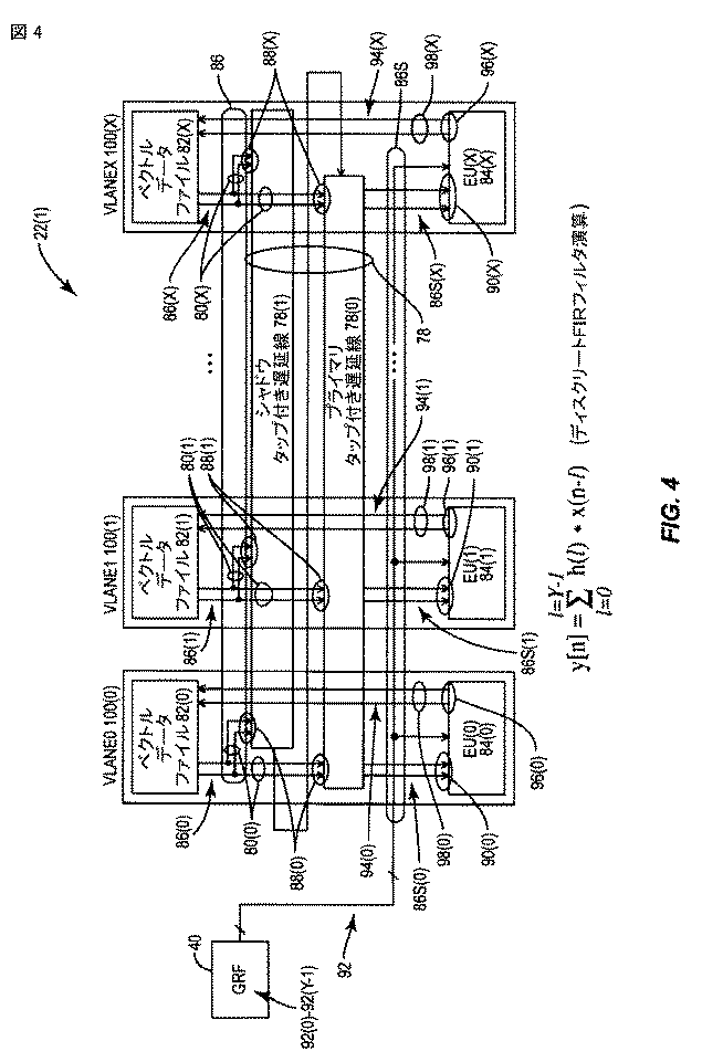
ここで、
nは入力信号サンプルの数であり、
x[n]はデジタル化入力信号66であり、
y[n]は基準信号であり、
lはサンプル数である。
here,
n is the number of input signal samples,
x [n] is the digitized
y [n] is a reference signal,
l is the number of samples.
[00133]後発相関ベクトル処理動作は、以下の式に従って提供される場合がある、 [00133] The late correlation vector processing operation may be provided according to the following equation:
ここで、
nは入力信号サンプルの数であり、
x[n]はデジタル化入力信号66であり、
y[n]は基準信号であり、
lはサンプル数である。
基準信号y[n](すなわち、基準ベクトルデータサンプル)は複素数であり得る。一態様では、VPE22(2)は、(たとえば、シーケンス番号発生器134から)基準信号を受信する場合がある。VPE22(2)は、オンタイム相関演算と後発相関演算とを実行するために受信された基準信号を直接使用する場合があり、その場合、上記の式における基準信号y[n]は、受信された基準信号を表す場合がある。代替として、VPE22(2)は、オンタイム相関演算と後発相関演算とを実行するために基準信号を使用する前に、受信された基準信号の複素共役を計算する場合があり、その場合、上記の式における基準信号y[n]は、受信された基準信号の共役を表す場合がある。
here,
n is the number of input signal samples,
x [n] is the digitized
y [n] is a reference signal,
l is the number of samples.
The reference signal y [n] (ie, the reference vector data sample) can be a complex number. In one aspect, VPE 22 (2) may receive a reference signal (eg, from sequence number generator 134). VPE 22 (2) may directly use the received reference signal to perform on-time correlation calculations and late correlation calculations, in which case the reference signal y [n] in the above equation is received. May represent a reference signal. Alternatively, VPE 22 (2) may calculate the complex conjugate of the received reference signal before using the reference signal to perform on-time correlation operations and late correlation operations, in which case The reference signal y [n] in the equation (1) may represent the conjugate of the received reference signal.
[00134]引き続き図11を参照すると、実行ユニット84(0)〜84(X)は、各々、実行ユニット84(0)〜84(X)内の中間相関出力ベクトルデータサンプルを供給するために、相関ベクトル処理動作の各処理ステージの間に、基準ベクトルデータサンプルセット130(0)〜130(X)を、シフトされた入力ベクトルデータサンプルセット86S(0)〜86S(X)のシフトされた入力ベクトルデータサンプル86S(0)、86S(1)、...86S(X)と乗算するように構成される。中間相関出力ベクトルデータサンプルセットは、実行ユニット84(0)〜84(X)の各々において累算される(すなわち、前に累算された相関出力ベクトルデータサンプルが現在の相関出力ベクトルデータサンプルに加算される)。これにより、実行ユニット84(0)〜84(X)によって生成された中間相関出力ベクトルデータサンプルセットを記憶しシフトする必要なしに、VPE22(2)によるさらなる使用および/または処理のためにそれぞれのベクトルデータファイル82(0)〜82(X)に戻して記憶されるべき入力ベクトルデータサンプルセット86(0)、86(1)、...86(X)ごとに、それぞれ、出力データフローパス98(0)〜98(X)上の実行ユニット出力96(0)〜96(X)上に実行ユニット84(0)〜84(X)によって供給される、最終的な、結果として生じる相関出力ベクトルデータサンプルセット132(0)〜132(X)がもたらされる。
[00134] With continued reference to FIG. 11, execution units 84 (0) -84 (X) each provide intermediate correlation output vector data samples in execution units 84 (0) -84 (X). During each processing stage of the correlation vector processing operation, the reference vector data sample sets 130 (0) to 130 (X) are shifted to the shifted input vector data sample sets 86S (0) to 86S (X).
[00135]さらに、図11のVPE22(2)内に設けられた同じ構成要素およびアーキテクチャが、図4のVPE22(1)内に設けられることに留意されたい。シーケンス番号発生器134は、フィルタ係数92(0)〜92(Y−1)または基準ベクトルデータサンプルセット130(0)〜130(X)と処理されるべき他のデータを供給することができるグローバルレジスタファイル40と、マルチプレクサ136によって加算および多重化される。したがって、図11のVPE22(2)は、前述のフィルタベクトル処理動作と、マルチプレクサ136の制御による、ここで説明され、下記でさらに詳細に説明される相関ベクトル処理動作の両方を提供することができる。マルチプレクサ136は、VPE22(2)によって実行されているベクトル命令に基づいて制御される選択器信号138によって制御され得る。フィルタベクトル命令の場合、選択器信号138は、実行ユニット84(0)〜84(X)に供給されるべきグローバルレジスタファイル40からのフィルタ係数92(0)〜92(Y−1)を供給するように構成され得る。相関ベクトル命令の場合、選択器信号138は、実行ユニット84(0)〜84(X)に供給されるべきシーケンス番号発生器134からの基準ベクトルデータサンプルセット130(0)〜130(X)を選択するように構成され得る。
[00135] Furthermore, it should be noted that the same components and architecture provided in VPE 22 (2) of FIG. 11 are provided in VPE 22 (1) of FIG. The
[00136]引き続き図11を参照すると、下記でより詳細に説明されるように、タップ付き遅延線78(0)、78(1)は、処理されているベクトル命令に従って制御されるようにプログラム可能である。相関ベクトル命令またはタップ付き遅延線78を利用しない他の命令が処理されていない場合、タップ付き遅延線78は、ベクトルデータファイル82(0)〜82(X)と実行ユニット84(0)〜84(X)との間の入力データフローパス80(0)〜80(X)に含まれないようにプログラムされ得る。この実施形態では、前に説明されたように、2つのタップ付き遅延線78、プライマリタップ付き遅延線78(0)およびシャドウタップ付き遅延線78(1)が設けられ、シャドウタップ付き遅延線78(1)はこの実施形態ではオプションである。前に説明されたように、タップ付き遅延線78がないと、実行ユニット84(0)〜84(X)にシフトされた中間入力ベクトルデータサンプルセットを再び供給するために、別個のシフティングプロセスが実行される必要があるはずであり、それにより、遅延時間が増大し、さらなる電力が消費される。さらに、相関ベクトル処理動作中、ベクトルデータファイル82(0)〜82(X)からのシフトされた入力ベクトルデータサンプルセット86S(0)〜86S(X)の再フェッチ遅延によって、VPE22(2)内の入力データフローパス80(0)〜80(X)および出力データフローパス98(0)〜98(X)の効率が制限されない。シフトされた入力ベクトルデータサンプルセット86S(0)〜86S(X)は、実行ユニット84(0)〜84(X)に局在するタップ付き遅延線78によって供給される。実行ユニット84(0)〜84(X)におけるベクトル処理は、データフローの制限ではなく、コンピュータリソースのみによって制限される。
[00136] With continued reference to FIG. 11, tapped delay lines 78 (0), 78 (1) are programmable to be controlled in accordance with the vector instruction being processed, as described in more detail below. It is. If no correlated vector instructions or other instructions that do not utilize the tapped
[00137]さらに、図11のVPE22(2)によって実行される相関ベクトル処理動作は、タップ付き遅延線78を利用することによってより精密にされ得るが、これは、実行ユニット84(0)〜84(X)内の中間相関処理ステージのための出力累算がベクトルデータファイル82(0)〜82(X)に記憶される必要がないからである。実行ユニット84(0)〜84(X)からベクトルデータファイル82(0)〜82(X)への中間ベクトルデータサンプルセットの記憶は、丸めをもたらす可能性がある。したがって、次の中間ベクトルデータサンプルセットがベクトル処理動作のために実行ユニット84(0)〜84(X)に供給されるとき、ベクトル処理動作の各乗算フェーズの間に任意の丸め誤差が伝搬および加算される。対照的に、図11のVPE22(2)の例では、実行ユニット84(0)〜84(X)によって計算された中間相関出力ベクトルデータサンプルセットは、ベクトルデータファイル82(0)〜82(X)に記憶される必要がない。前の中間相関出力ベクトルデータサンプルセットは、次の相関出力ベクトルデータサンプルセットのための中間相関出力ベクトルデータサンプルセットと累算され得るが、これは、タップ付き遅延線78が、処理されるべきベクトル処理動作の間に、実行ユニット84(0)〜84(X)にシフトされた入力ベクトルデータサンプルセット86S(0)〜86S(X)を供給するからであり、結果は前の相関出力ベクトルデータサンプルセットのための前のベクトルデータサンプルセットと累算される。
[00137] Furthermore, the correlation vector processing operations performed by VPE 22 (2) of FIG. 11 may be made more precise by utilizing tapped
[00138]上記図4のVPE22(1)内に設けられた構成要素の前の説明は、図11のVPE22(2)に等しく適用可能であり、したがって再び記載されない。 [00138] The previous description of the components provided in VPE 22 (1) of FIG. 4 above is equally applicable to VPE 22 (2) of FIG. 11, and therefore will not be described again.
[00139]図11のVPE22(2)のさらなる詳細および特徴、ならびにこの実施形態における入力データフローパス80(0)〜80(X)内の実行ユニット84(0)〜84(X)にシフトされた入力ベクトルデータサンプルセット86S(0)〜86S(X)を供給するためのタップ付き遅延線78のさらなる説明が次に記載される。この関連で、図12Aおよび図12Bは、例示的な相関ベクトル命令に従って、タップ付き遅延線78を利用する図11のVPE22(2)において実行され得る例示的な相関ベクトル処理動作140を示すフローチャートである。図12Aおよび図12Bは、例示的な相関/共分散ベクトル処理動作に従って、インターリーブされたオンタイムおよび後発の入力ベクトルデータサンプルセットがフェッチされる、図11のVPE22(2)において並列に実行され得る例示的な相関/共分散ベクトル処理動作を示すフローチャートである。
[00139] Further details and features of VPE 22 (2) of FIG. 11 and shifted to execution units 84 (0) -84 (X) in input data flow paths 80 (0) -80 (X) in this embodiment. Further description of tapped
[00140]図13〜図17Bにおいて提供される例を参照して、図12Aおよび図12Bの相関ベクトル処理動作140において実行される例示的なタスクが記載される。図12Aを参照すると、相関ベクトル命令に従って相関ベクトル処理動作140において処理されるべき入力ベクトルデータサンプルセット86(0)〜86(X)が、相関ベクトル処理動作140のために、ベクトルデータファイル82(0)〜82(X)から入力データフローパス80(0)〜80(X)の中にフェッチされる(ブロック142)。図11のVPE22(2)に関して上記で説明されたように、入力ベクトルデータサンプルセット86(0)〜86(X)は、実行ユニット84(0)〜84(X)内のシーケンス番号発生器134から受信された基準ベクトルデータサンプルセット130(0)〜130(X)と乗算される。たとえば、図13は、シーケンス番号発生器134内の基準ベクトルデータサンプルセット130(0)〜130(X)を示す。この例では、入力ベクトルデータサンプルセット86(0)〜86(X)内の16個の入力ベクトルデータサンプル86(0)、86(1)、...86(15)と相関されるべき、グローバルレジスタファイル40に記憶された16個の基準ベクトルデータサンプル130(0)、130(1)、...130(15)が存在する。上記で前に説明された図6Bは、ベクトルデータファイル82(0)〜82(X)に記憶された例示的な入力ベクトルデータサンプルセット86(0)〜86(X)を示したが、それはこの例においても適用可能であり、したがって、ここでは再び記載されない。
[00140] With reference to the examples provided in FIGS. 13-17B, exemplary tasks performed in the correlation
[00141]相関ベクトル処理動作140において相関されるべき入力ベクトルデータサンプルセット86(0)〜86(X)および基準ベクトルデータサンプルセット130(0)〜130(X)の幅に応じて、ベクトル命令のプログラミングに従う相関ベクトル処理動作140を提供するために、図11のVPE22(2)内のベクトルデータレーン100(0)〜100(X)の1つ、いくつか、またはすべてが利用され得る。ベクトルデータファイル82(0)〜82(X)の幅全体が必要な場合、すべてのベクトルデータレーン100(0)〜100(X)が相関ベクトル処理動作140に利用され得る。相関ベクトル処理動作140は、相関ベクトル処理動作140に利用され得るベクトルデータレーン100(0)〜100(X)のサブセットを必要とするにすぎない場合があることに留意されたい。これは、入力ベクトルデータサンプルセット86(0)〜86(X)の幅がすべてのベクトルデータファイル82(0)〜82(X)の幅よりも小さいからであり得るし、ここで、相関ベクトル処理動作140と並列に実行されるべき他のベクトル処理動作にさらなるベクトルデータレーン100を利用することが望ましい。現在の例を説明する目的で、相関ベクトル処理動作140において利用される入力ベクトルデータサンプルセット86(0)〜86(X)および基準ベクトルデータサンプルセット130(0)〜130(X)が、VPE22(2)内のすべてのベクトルデータレーン100(0)〜100(X)を要すると想定する。
[00141] Vector instructions depending on the width of the input vector data sample sets 86 (0) -86 (X) and the reference vector data sample sets 130 (0) -130 (X) to be correlated in the correlation
[00142]図12Aに戻って参照すると、相関ベクトル処理動作140のための第1の入力ベクトルデータサンプルセット86S(0)〜86(X)としてタップ付き遅延線78にロードされるために、フェッチされた入力ベクトルデータサンプルセット86(0)〜86(X)が、ベクトルデータファイル82(0)〜82(X)から入力データフローパス80(0)〜80(X)に供給される(ブロック144)。入力ベクトルデータサンプルセット86(0)〜86(X)は、相関ベクトル処理動作140のために実行ユニット84(0)〜84(X)によって処理されるべき入力ベクトルデータサンプルセット86(0)〜86(X)として、プライマリタップ付き遅延線78(0)の中にロードされる。プライマリタップ付き遅延線78(0)の中にロードされた入力ベクトルデータサンプルセット86(0)〜86(X)は、相関ベクトル処理動作140の最初の動作のためにシフトされない。次の入力ベクトルデータサンプルセット86N(0)〜86N(X)も、実行ユニット84(1)〜84(X)によって処理されるべき次の入力ベクトルデータサンプルセット86N(0)〜86N(X)として、シャドウタップ付き遅延線78(1)の中にロードされ得る。上記で前に説明され、下記でさらに詳細に説明されるように、タップ付き遅延線78の目的は、相関ベクトル処理動作140の動作の間に、次の相関演算のために実行ユニット84(0)〜84(X)にシフトされた入力ベクトルデータサンプルセット86S(0)〜86S(X)を供給するために、入力ベクトルデータサンプルセット86(0)〜86(X)のシフトを提供することである。実行ユニット84(0)〜84(X)によって実行される相関ベクトル処理動作140の各処理ステージの間に、実行ユニット84(0)〜84(X)にシフトされた入力ベクトルデータサンプルセット86S(0)〜86S(X)を供給するために、入力ベクトルデータサンプル86はプライマリタップ付き遅延線78(0)内でシフトされる。このようにして、入力ベクトルデータサンプルセット86(0)〜86(X)は、相関ベクトル処理動作140の相関演算ごとに、記憶、ベクトルデータファイル82(0)〜82(X)内でシフト、および再フェッチされる必要がない。
[00142] Referring back to FIG. 12A, fetch to be loaded into the tapped
[00143]この関連で、図14は、図11のVPE22(2)内に設けられ得る例示的なタップ付き遅延線78を示す。この実施形態では、タップ付き遅延線78は、シャドウタップ付き遅延線78(1)とプライマリタップ付き遅延線78(0)とを備える。上記で前に説明されたように、この例におけるプライマリタップ付き遅延線78(0)は、入力ベクトルデータサンプル86の解像度が8ビット長に落ちることを可能にするために、複数の8ビットプライマリパイプラインレジスタ120から構成される。実行ユニット84(0)〜84(X)によって処理される最初の入力ベクトルデータサンプルセット86(0)〜86(X)は、相関ベクトル処理動作140の最初の相関演算のためにこの例ではシフトされない。実行ユニット84(0)〜84(X)が相関ベクトル処理動作140のために次の相関演算を処理するとき、プライマリタップ付き遅延線78(0)に記憶された入力ベクトルデータサンプルセット86(0)〜86(X)内の入力ベクトルデータサンプル86は、シフトされた入力ベクトルデータサンプルセット86S(0)〜86S(X)になるために、図14の矢印によって示されたように、プライマリパイプラインレジスタ120(0)〜120(4X+3)内でシフトされる。このようにして、実行ユニット84(0)〜84(X)は、ベクトルデータファイル82(0)〜82(X)から入力ベクトルデータサンプルセット86(0)〜86(X)を記憶、シフト、および再フェッチする必要なしに、シフトされた入力ベクトルデータサンプルセット86S(0)〜86S(X)を受信し、それらの相関ベクトル処理動作140を実行することによって、十分利用される。
[00143] In this regard, FIG. 14 illustrates an exemplary tapped
[00144]相関ベクトル処理動作140のためにプライマリタップ付き遅延線78(0)およびシャドウタップ付き遅延線78(1)において実行されるシフトの回数は、相関されるべきサンプルの数に依存する。ベクトルデータファイル82(0)〜82(X)からプライマリタップ付き遅延線78(0)およびシャドウタップ付き遅延線78(1)の中にフェッチされた入力ベクトルデータサンプルセット86(0)〜86(X)内の入力ベクトルデータサンプル86の数が、相関ベクトル処理動作140における相関演算の数よりも大きい場合、実行ユニット84(0)〜84(X)は、任意のさらなる入力ベクトルデータサンプルセット86(0)〜86(X)がベクトルデータファイル82(0)〜82(X)から再フェッチされることなく、相関ベクトル処理動作140を実行することができる。しかしながら、相関ベクトル処理動作140における相関演算の数が、ベクトルデータファイル82(0)〜82(X)からプライマリタップ付き遅延線78(0)およびシャドウタップ付き遅延線78(1)の中にフェッチされた入力ベクトルデータサンプルセット86(0)〜86(X)内の入力ベクトルデータサンプル86の数よりも大きい場合、相関ベクトル処理動作140の一部として、さらなる入力ベクトルデータサンプルセット86(0)〜86(X)がベクトルデータファイル82(0)〜82(X)からフェッチされ得る。
[00144] The number of shifts performed in primary tapped delay line 78 (0) and shadow tapped delay line 78 (1) for correlation
[00145]この実施形態では、プライマリパイプラインレジスタ120(0)〜120(4X+3)はまとめて、ベクトルデータファイル82(0)〜82(X)の幅である。15に等しい「X」を有する幅が512ビットであるベクトルデータファイル82(0)〜82(X)の例では、512ビット(すなわち、64個のレジスタ×各8ビット)の合計幅を提供するために、各々が8ビットの幅である64個の合計プライマリパイプラインレジスタ120(0)〜120(63)が存在する。したがって、この例では、プライマリタップ付き遅延線78(0)は、1つの入力ベクトルデータサンプルセット86(0)〜86(X)の幅全体を記憶することが可能である。この例では、8ビット幅のプライマリパイプラインレジスタ120(0)〜120(4X+3)を設けることによって、入力ベクトルデータサンプルセット86(0)〜86(X)は、8ビット相関ベクトル処理動作のために8ビットベクトルデータサンプルサイズにシフトダウンされ得る。たとえば、16ビットまたは32ビットのサンプルなどのより大きい入力ベクトルデータサンプル86のサイズが相関ベクトル処理動作140に望ましい場合、入力ベクトルデータサンプルセット86(0)〜86(X)は、プライマリパイプラインレジスタ120(0)〜120(4X+3)において、1度に2つのプライマリパイプラインレジスタ120によってシフトされ得る。
[00145] In this embodiment, primary pipeline registers 120 (0) -120 (4X + 3) are collectively the width of vector data files 82 (0) -82 (X). In the example of a vector data file 82 (0) -82 (X) having a width of “X” equal to 15 and 512 bits, it provides a total width of 512 bits (ie, 64 registers × 8 bits each) Therefore, there are 64 total primary pipeline registers 120 (0) -120 (63), each 8 bits wide. Accordingly, in this example, the primary tapped delay line 78 (0) can store the entire width of one input vector data sample set 86 (0) -86 (X). In this example, by providing 8-bit wide primary pipeline registers 120 (0) to 120 (4X + 3), the input vector data sample sets 86 (0) to 86 (X) are for 8-bit correlation vector processing operations. Can be shifted down to 8-bit vector data sample size. For example, if a larger input
[00146]図15Aは、相関ベクトル処理命令140の第1のクロックサイクル(CYCLE0)の間に、ベクトルデータファイル82(0)〜82(X)からプライマリタップ付き遅延線78(0)の中にロードされた入力ベクトルデータサンプルセット86(0)〜86(X)を示す。最初の入力ベクトルデータサンプルセット86(0)〜86(X)が入力ベクトルデータサンプルX1〜X32としてプライマリタップ付き遅延線78(0)の中にロードされるが、64個の入力ベクトルデータサンプルが供給される。プライマリパイプラインレジスタ120(0)〜120(2X+1)(図14も参照)は、入力ベクトルデータサンプルセット86(0)〜86(X)からオンタイム入力ベクトルデータサンプルおよび後発入力ベクトルデータサンプルをロードされる。たとえば、プライマリタップ付き遅延線78(0)の中に(および下記で後により詳細に説明されるように、シャドウタップ付き遅延線78(1)の中にも)、入力ベクトルデータサンプルセット86(0)〜86(X)のオンタイム入力ベクトルデータサンプルと後発入力ベクトルデータサンプルとをロードするために、特殊なベクトル命令がサポートされる場合がある。たとえば、プライマリパイプラインレジスタ122(0)、122(1)、122(2X+2)、および122(2X+3)はまとめて、入力ベクトルデータサンプル86(0)を含んでいる。プライマリパイプラインレジスタ122(0)、122(1)は、X(0)およびX(1)であるオンタイム入力ベクトルデータサンプル86OT(0)を含んでおり、ここで「OT」は「オンタイム」を意味する。プライマリパイプラインレジスタ122(2X+2)、122(2X+3)は、X(1)およびX(2)である後発入力ベクトルデータサンプル86L(0)を含んでおり、ここで「L」は「後発」を意味する。プライマリタップ付き遅延線78(0)内のこの入力ベクトルデータサンプル86の記憶パターンは、他のプライマリパイプラインレジスタ122(2)〜122(2X+1)および122(2X+4)〜122(4X+3)について繰り返される(図14参照)。
[00146] FIG. 15A illustrates that during the first clock cycle (CYCLE0) of the correlation
[00147]図14に戻って参照すると、シャドウタップ付き遅延線78(1)もタップ付き遅延線78内に設けられる。シャドウタップ付き遅延線78(1)は、次のベクトル処理動作のためにベクトルデータファイル82(0)〜82(X)から次の入力ベクトルデータサンプルセット86N(0)〜86N(X)をラッチまたは輸送するために利用され得る。シャドウタップ付き遅延線78(1)はまた、入力ベクトルデータサンプルの解像度が、プライマリタップ付き遅延線78(0)と同様に8ビット長に落ちることを可能にするために、複数の8ビットシャドウパイプラインレジスタ122から構成される。シャドウパイプラインレジスタ122はまとめて、この例では512ビットであるベクトルデータファイル82(0)〜82(X)の幅であり、その結果、シャドウタップ付き遅延線78(1)も、プライマリタップ付き遅延線78(0)のように、1つの入力ベクトルデータサンプルセット86(0)〜86(X)の幅全体を記憶することが可能である。したがって、この実施形態では、プライマリタップ付き遅延線78(0)に含まれるシャドウパイプラインレジスタ122(0)〜122(4X+3)の数は、合計16であるベクトルデータレーン100(0)〜100(X)の数の4倍であり、この例では各ベクトルデータレーン100(0)〜100(X)が各々32ビットをサポートすることが可能である。したがって、プライマリパイプラインレジスタ120の数も、この例では合計512ビット(すなわち、64個のレジスタ×各8ビット)用に合計64である。
[00147] Referring back to FIG. 14, a shadow tapped delay line 78 (1) is also provided in the tapped
[00148]図15Bは、相関ベクトル処理命令140の第2のクロックサイクル(CYCLE1)の間に、シャドウタップ付き遅延線78(1)の中にロードされた次の入力ベクトルデータサンプルセット86N(0)〜86N(X)を示す。相関ベクトル処理動作140の実行をセットアップするために、ベクトルデータファイル82(0)〜82(X)からの最初の入力ベクトルデータサンプルセット86(0)〜86(X)がプライマリタップ付き遅延線78(0)の中にロードされた後に、次の入力ベクトルデータサンプルセット86N(0)〜86N(1)がシャドウタップ付き遅延線78(1)の中にロードされる。この次の入力ベクトルデータサンプルセット86N(0)〜86N(X)が、オンタイム入力ベクトルデータサンプル86OTと後発入力ベクトルデータサンプル86Lの両方とともに、入力ベクトルデータサンプルX(32)〜X(63)としてシャドウタップ付き遅延線78(1)の中にロードされる。この例では、上記で説明されたプライマリタップ付き遅延線78(0)において提供される記憶パターンのように、X(32)およびX(33)が入力ベクトルデータサンプル86(0)のオンタイム入力ベクトルデータサンプル86OTを形成し、X(33)およびX(34)が入力ベクトルデータサンプル86(0)の後発入力ベクトルデータサンプル86Lを形成することに留意されたい。入力ベクトルデータサンプル86を一緒にグループ化して、入力ベクトルデータサンプルセット86(0)〜86(X)を形成するために、他のパターンが提供される可能性がある。シーケンス番号発生器134からの基準ベクトルデータサンプルセット130(0)〜130(X)から、相関ベクトル処理動作140の第1の処理ステージの間に相関された基準ベクトルデータサンプル130(すなわち、Y(0)およびY(1))はまた、相関ベクトル処理動作140において使用するための図15Bの実行ユニット84(0)〜84(X)へのレジスタ(「C」)内で供給されるものとして示される。
[00148] FIG. 15B illustrates the next input vector data sample set 86N (0) loaded into the shadow tapped delay line 78 (1) during the second clock cycle (CYCLE1) of the correlation vector processing instruction 140. ) To 86N (X). To set up the execution of the correlation
[00149]図14に戻って参照すると、相関ベクトル処理動作140の各処理ステージの間に、入力ベクトルデータサンプルセット86(0)〜86(X)内の入力ベクトルデータサンプル86がプライマリタップ付き遅延線78(0)内でシフトされるとき、シャドウパイプラインレジスタ122に記憶された次の入力ベクトルデータサンプル86Nも、シャドウタップ付き遅延線78(1)のシャドウパイプラインレジスタ122内でシフトされる。この例では、入力ベクトルデータサンプルセット86(0)〜86(X)の入力ベクトルデータサンプル86は、オンタイムバージョンおよび後発バージョンとして記憶されるので、図14のタップ付き遅延線78(0)と78(1)との間で提供されるシフトパターンは、図7のタップ付き遅延線78(0)と78(1)との間で提供されるシフトパターンとは異なる。図14に示されたように、オンタイム入力ベクトルデータサンプル86OTは、シャドウタップ付き遅延線78(1)内のシャドウパイプラインレジスタ122(0)から、プライマリタップ付き遅延線78(0)内のプライマリパイプラインレジスタ120(2X+1)にシフトされる。同じく、後発入力ベクトルデータサンプル86Lは、シャドウタップ付き遅延線78(1)内のシャドウパイプラインレジスタ122(2X+2)から、プライマリタップ付き遅延線78(0)内のプライマリパイプラインレジスタ120(4X+3)にシフトされる。このようにして、入力ベクトルデータサンプル86のシフトが相関ベクトル処理動作140の間に発生するとき、オンタイム入力ベクトルデータサンプル86OTおよび後発入力ベクトルデータサンプル86OTは、タップ付き遅延線78(0)、78(1)内で互いから隔離され続ける。
[00149] Referring back to FIG. 14, during each processing stage of the correlation
[00150]相関ベクトル処理動作140の処理ステージが実行ユニット84(0)〜84(X)において進行し、最終的に、シャドウタップ付き遅延線78(1)に最初に記憶された次の入力ベクトルデータサンプルセット86N(0)〜86N(X)全体は、処理のために実行ユニット84(0)〜84(X)に供給されるために、プライマリタップ付き遅延線78(0)の中に完全にシフトされる。このようにして、相関ベクトル処理動作140が現在の入力ベクトルデータサンプルセット86(0)〜86(X)に対して完了した後、実行ユニット84(0)〜84(X)は、次いで、必要な場合、遅延なく、次の相関ベクトル処理動作140のための現在の入力ベクトルデータサンプルセット86(0)〜86(X)として、プライマリタップ付き遅延線78(0)に記憶された前の次の入力ベクトルデータサンプルセット86N(0)〜86N(X)を供給され得る。
[00150] The processing stage of correlation
[00151]最初の入力ベクトルデータサンプルセット86(0)〜86(X)および次の入力ベクトルデータサンプルセット86N(0)〜86N(X)が、それぞれ、プライマリタップ付き遅延線78(0)およびシャドウタップ付き遅延線78(1)の中にロードされた後、図15Bに示されたように、プライマリタップ付き遅延線78(0)内に供給された最初の入力ベクトルデータサンプルセット86(0)〜86(X)は、相関ベクトル処理動作140の最初の処理ステージにおいて処理されるために、それぞれの実行ユニット84(0)〜84(X)に供給される(図12Aのブロック146)。最初の入力ベクトルデータサンプルセット86(0)〜86(X)は、実行ユニット84(0)〜84(X)によって処理されている現在の入力ベクトルデータサンプルセット86(0)〜86(X)になる。図11のVPE22(2)において示されたように、現在の入力ベクトルデータサンプル86(0)は実行ユニット84(0)に供給され、現在の入力ベクトルデータサンプル86(1)は実行ユニット84(1)に供給され、以下同様である。相関ベクトル処理動作140の現在の処理ステージにおいて、入力ベクトルデータサンプルセット86(0)〜86(X)と相関されるべき基準ベクトルデータ入力サンプル130(0)〜130(X)が実行ユニット84(0)〜84(X)に供給される(図12Aのブロック148)。
[00151] The first input vector data sample set 86 (0) -86 (X) and the next input vector data sample set 86N (0) -86N (X) are respectively the primary tapped delay line 78 (0) and After loading into the shadow tapped delay line 78 (1), the first input vector data sample set 86 (0) supplied in the primary tapped delay line 78 (0) as shown in FIG. 15B. ) -86 (X) are provided to respective execution units 84 (0) -84 (X) for processing in the first processing stage of the correlation vector processing operation 140 (block 146 of FIG. 12A). The first input vector data sample sets 86 (0) -86 (X) are the current input vector data sample sets 86 (0) -86 (X) being processed by execution units 84 (0) -84 (X). become. As shown in VPE 22 (2) of FIG. 11, the current input vector data sample 86 (0) is provided to execution unit 84 (0), and the current input vector data sample 86 (1) is provided to execution unit 84 (0). 1), and so on. At the current processing stage of correlation
[00152]次に、実行ユニット84(0)〜84(X)が、相関ベクトル処理動作140(図12Aのブロック150)を実行する。より詳細には、実行ユニット84(0)〜84(X)は、演算:オンタイム入力ベクトルデータサンプル86OTのためのR(OT)[n]=y[0]*x[n]および後発入力ベクトルデータサンプル86LのためのR(L)[n]=y[1]*x[1+n]に従って、最初の処理ステージの間に現在の入力ベクトルデータサンプルセット86(0)〜86(X)を基準ベクトルデータサンプル130と乗算し、ここで、y[]は指定された基準ベクトルデータサンプル130であり、x[n]は現在の入力ベクトルデータサンプルセット86(0)〜86(X)である。相関の結果は、現在のオンタイム相関出力ベクトルデータサンプルセットR(OT)[n]および現在の後発相関出力ベクトルデータサンプルセットR(L)[n]である。次いで、実行ユニット84(0)〜84(X)が、新しい前の入力ベクトルデータサンプルセット86(0)〜86(X)を供給するために、各現在の、結果として生じる相関ベクトルデータサンプルセットを、実行ユニット84(0)〜84(X)によって計算された前の、結果として生じる相関ベクトルデータサンプルセットと累算する(図12Bのブロック152)。相関ベクトル処理動作140の最初の処理ステージでは、前の、結果として生じる相関出力ベクトルデータサンプルセット132(0)〜132(X)は存在しない。したがって、相関ベクトル処理動作140の2番目の次の処理ステージのために、最初/現在の、結果として生じる相関出力ベクトルデータサンプルセット132(0)〜132(X)が前の入力ベクトルデータサンプルセット86(0)〜86(X)になるにすぎない。
[00152] Next, execution units 84 (0) -84 (X) perform a correlation vector processing operation 140 (block 150 of FIG. 12A). More specifically, execution units 84 (0) -84 (X) are operated on: R (OT) [n] = y [0] * x [n] and late input for on-time input vector data sample 86OT. According to R (L) [n] = y [1] * x [1 + n] for the
[00153]相関ベクトル処理動作140のすべての処理ステージが完了した場合(図12Bのブロック154)、ベクトルデータファイル82(0)〜82(X)に供給され記憶されるために、出力データフローパス98(0)〜98(X)内の、結果として生じる相関出力ベクトルデータサンプルセット132(0)〜132(X)として、累算された前の、結果として生じる相関出力ベクトルデータサンプルセット132(0)〜132(X)が供給される(図12Bのブロック157)。相関ベクトル処理動作140のすべての処理ステージが完了していなかった場合(図12Aのブロック154)、シフトされた入力ベクトルデータサンプルセット86S(0)〜86S(X)を供給するために、シフトされた入力ベクトルデータサンプルセット86S(0)〜86S(X)が、相関ベクトル処理動作140のための次の場所にタップ付き遅延線78(0)、78(1)内でシフトされる(図12Bのブロック156)。シフトされた入力ベクトルデータサンプルセット86S(0)〜86S(X)は、前の、結果として生じる相関出力ベクトルデータサンプルセット132(0)〜132(X)と累算されるように、次の、結果として生じる相関出力ベクトルデータサンプルセット132(0)〜132(X)を計算するために供給される。タップ付き遅延線78(0)、78(1)内で入力ベクトルデータサンプル86をシフトすることは、図14に関して詳細に上記で前述された。
[00153] When all processing stages of the correlation
[00154]図15Cは、次の相関処理動作140、オンタイム入力ベクトルデータサンプル86SOTのためのR(OT)[n]=y[2]*x[2+n]および後発入力ベクトルデータサンプル86SLのためのR(L)[n]=y[3]*x[3+n]のための新たなシフトされた入力ベクトルデータサンプルセット86S(0)〜86S(X)になるために、相関ベクトル処理動作140の2番目の処理ステージにおいて、入力ベクトルデータサンプルセット86(0)〜86(X)がシフトされたときのタップ付き遅延線78のコンテンツを示す。プライマリタップ付き遅延線78(0)内の入力ベクトルデータサンプルセット86(0)〜86(X)が、2つの入力ベクトルデータサンプル86によってシフトされる。たとえば、x(2)およびX(3)の図15Bの入力ベクトルデータサンプル86OT(1)が、次に図15Cの入力ベクトルデータサンプル86S(0)の中にシフトされる。シフトされた入力ベクトルデータサンプルセット86S(0)〜86S(X)は、現在の入力ベクトルデータサンプルセット86(0)〜86(X)になる。実行ユニット84(0)〜84(X)に供給された基準ベクトルデータサンプル130はまた、この例ではY(2)およびY(3)である基準ベクトルデータサンプル130である。
[00154] FIG. 15C illustrates the
[00155]引き続き図12Bを参照すると、次の基準ベクトルデータサンプル130と乗算されるために、プライマリタップ付き遅延線78(0)から(およびシャドウタップ付き遅延線78(1)の一部分から)実行ユニット84(0)〜84(X)に次のシフトされた入力ベクトルデータサンプルセット86S(0)〜86S(X)を供給する(図12Aのブロック150)ことによってプロセスが繰り返し、結果として生じる相関出力ベクトルデータサンプルセット132(0)〜132(X)が、前の、結果として生じる相関出力ベクトルデータサンプルセット132(0)〜132(X)と累算される(図12Bのブロック152)。図15Dは、例示的な相関ベクトル処理動作140の最後の処理ステージの間に、タップ付き遅延線78(0)、78(1)内に存在する入力ベクトルデータサンプル86の状態を示す。この例では、図15Dに示されたように、タップ付き遅延線78のフルデータ幅は、入力ベクトルデータサンプルセット86(0)〜86(X)に利用されたが、オンタイム入力ベクトルデータサンプル86OTと後発入力ベクトルデータサンプル86Lとの間で分割されるので、相関ベクトル処理動作140のための16個の処理ステージが存在した。図15Dに示されたように、Y(30)およびY(31)は、相関ベクトル処理動作140における最後の基準ベクトルデータサンプル130(X)であり、それは、図13の例では基準ベクトルセータサンプル130(15)である。シフトされた入力ベクトルデータサンプルセット86S(0)〜86S(X)は(この例ではベクトルデータレーン100(0)〜100(X)の幅である)16回シフトされており、その結果、相関ベクトル処理動作140のための最後の16番目の処理ステージにおいて、入力ベクトルデータサンプルX(30)およびX(31)がプライマリタップ付き遅延線78(0)内のシフトされた入力ベクトルデータサンプル86S(0)に記憶される。
[00155] With continued reference to FIG. 12B, run from primary tapped delay line 78 (0) (and from a portion of shadow tapped delay line 78 (1)) to be multiplied with the next reference
[00156]図16は、上記の例における例示的な16個の相関ベクトル処理ステージが完全に実行された後の、図11のVPE22(2)内の実行ユニット84(0)〜84(X)内の累算器のコンテンツ(すなわち、結果として生じる相関出力ベクトルデータサンプル132)の概略図である。結果として生じる相関出力ベクトルデータサンプルセットは、132(0)〜132(X)として示される。この例では、各実行ユニット84(0)〜84(X)は、ベクトルデータレーン100(0)〜100(X)ごとに並列に配置された4つの累算器を有するので、累算器Acc0〜Acc3が図16に示されている。累算された、結果として生じる出力ベクトルデータサンプルは、さらなる分析および/または処理のためにそこに記憶されるべき全体の結果として生じる相関出力ベクトルデータサンプルセット132(0)〜132(X)として、ベクトルデータファイル82(0)〜82(X)に出力データフローパス98(0)〜98(X)上で供給され得る。必要な場合、ベクトルデータファイル82(0)〜82(X)からベクトルユニットデータメモリ32(図2参照)に、結果として生じる相関出力ベクトルデータサンプルセット132(0)〜132(X)の行を移動するために、特殊なベクトル命令がVPE22(2)によってサポートされる場合がある。 [00156] FIG. 16 illustrates execution units 84 (0) -84 (X) in VPE 22 (2) of FIG. 11 after the exemplary 16 correlation vector processing stages in the above example have been fully executed. FIG. 6 is a schematic diagram of the contents of the accumulators in (ie, the resulting correlation output vector data sample 132). The resulting correlation output vector data sample set is shown as 132 (0) -132 (X). In this example, each execution unit 84 (0) -84 (X) has four accumulators arranged in parallel for each of the vector data lanes 100 (0) -100 (X), so the accumulator Acc0 ~ Acc3 is shown in FIG. The resulting output vector data samples accumulated are as the entire resulting correlation output vector data sample set 132 (0) -132 (X) to be stored there for further analysis and / or processing. , Vector data files 82 (0) -82 (X) may be provided on output data flow paths 98 (0) -98 (X). If necessary, the rows of the resulting correlation output vector data sample sets 132 (0) -132 (X) are transferred from the vector data files 82 (0) -82 (X) to the vector unit data memory 32 (see FIG. 2). In order to move, special vector instructions may be supported by VPE 22 (2).
[00157]上述された、結果として生じるフィルタベクトル出力データサンプルセット94(0)〜94(X)と、結果として生じる相関出力ベクトルデータサンプルセット132(0)〜132(X)とを含む、実行ユニット84(0)〜84(X)によって供給される、結果として生じる出力ベクトルデータサンプルセットは、VPEによって実行されるベクトル命令に応じて、異なるインターリーブされたフォーマットでベクトルデータファイル82(0)〜82(X)、82(31)に戻されて記憶され得る。各々32ビット幅であるベクトルデータファイル82(0)〜82(X)を提供するために、この例では「X」は31に等しい。たとえば、図17Aに示されたように、結果として生じる出力ベクトルデータサンプルセット158(0)〜158(X)、158(31)は、それらの実数(「q」)成分および虚数(「i」)成分によって分離されたベクトルデータファイル82(0)〜82(X)に記憶され得る。結果として生じる出力ベクトルデータサンプルセット158(0)〜158(X)は、この例では158(0)、158(1)、...、および158(X)である、「X+1」個の、結果として生じる出力ベクトルデータサンプル158から構成される。次のベクトル命令が、入力ベクトルデータサンプルセットとして、結果として生じる出力ベクトルデータサンプルセット158(0)〜158(X)、158(31)の実数成分および虚数成分に対して演算する場合など、効率目的でそれらの実数(「q」)成分および虚数(「i」)成分によって分離された、結果として生じる出力ベクトルデータサンプルセット158(0)〜158(X)、158(31)を記憶することはより効率的であり得る。または、結果として生じる出力ベクトルデータサンプル158のその実数成分および虚数成分への分離のように、ベクトルデータファイル82内に、結果として生じる出力ベクトルデータサンプル158を記憶することが可能ではない場合がある。たとえば、16ビットベクトルデータサンプルが別の16ビットベクトルデータサンプルと乗算される場合、32ビットの結果として生じるベクトルデータサンプルがもたらされる。たとえば、32ビットの結果として生じる出力ベクトルデータサンプル158は、図17AのY0であり得る。Y0の虚数成分Y0.i158(I)はベクトルデータファイル82(0)のADDRESS「0」に記憶され得るし、Y0の実数成分Y0.q158(Q)はADDRESS「A」などの別のADDRESSに記憶され得る。
[00157] An implementation comprising the resulting filter vector output data sample sets 94 (0) -94 (X) and the resulting correlation output vector data sample sets 132 (0) -132 (X), as described above. The resulting output vector data sample sets supplied by units 84 (0) -84 (X) are in different interleaved formats depending on vector instructions executed by the VPE, in vector data files 82 (0)- 82 (X) and 82 (31) can be stored back. In this example, “X” is equal to 31 to provide vector data files 82 (0) -82 (X) that are each 32 bits wide. For example, as shown in FIG. 17A, the resulting output vector data sample sets 158 (0) -158 (X), 158 (31) have their real (“q”) components and imaginary numbers (“i”). ) May be stored in vector data files 82 (0) -82 (X) separated by components. The resulting output vector data sample sets 158 (0) -158 (X) are 158 (0), 158 (1),. . . , And 158 (X), consisting of “X + 1” resulting output
[00158]図17Aの結果として生じる出力ベクトルデータサンプルセット158(0)〜158(X)、158(31)は、偶数および奇数の結果として生じる出力ベクトルデータサンプルによってインターリーブされたベクトルデータファイル82(0)〜82(X)、82(31)に記憶される可能性がある。これは図17Bにおける例によって示される。図17Bに示されたように、結果として生じる出力ベクトルデータサンプルY0〜Y31 158(0)〜158(X)、158(31)は、ベクトルデータファイル82(0)〜82(31)内のADDRESS「0」およびADDRESS「A」の中の偶数および奇数のベクトルデータサンプルによってインターリーブされたフォーマットで記憶される。結果として生じる出力ベクトルデータサンプルY0 158(0)は、ベクトルデータファイル82(0)内のADDRESS「0」に記憶される。結果として生じる出力ベクトルデータサンプルY1 158(1)は、ベクトルデータファイル82(1)内のADDRESS「0」に記憶されないが、ベクトルデータファイル82(0)内のADDRESS「A」に記憶される。結果として生じる出力ベクトルデータサンプルY2 158(2)は、ベクトルデータファイル82(1)内のADDRESS「0」に記憶され、以下同様である。 [00158] The resulting output vector data sample sets 158 (0) -158 (X), 158 (31) of FIG. 17A are interleaved with the vector data file 82 (interleaved with even and odd resulting output vector data samples. 0) to 82 (X) and 82 (31). This is illustrated by the example in FIG. 17B. As shown in FIG. 17B, the resulting output vector data samples Y0-Y31 158 (0) -158 (X), 158 (31) are ADDRESS in the vector data files 82 (0) -82 (31). Stored in a format interleaved with even and odd vector data samples in "0" and ADDRESS "A". The resulting output vector data sample Y0 158 (0) is stored in ADDRESS “0” in the vector data file 82 (0). The resulting output vector data sample Y1 158 (1) is not stored in ADDRESS “0” in vector data file 82 (1), but is stored in ADDRESS “A” in vector data file 82 (0). The resulting output vector data sample Y2 158 (2) is stored in ADDRESS “0” in the vector data file 82 (1), and so on.
[00159]いくつかのワイヤレスベースバンド動作は、データサンプルが処理される前にフォーマット変換されることを必要とする。たとえば、図17Aおよび図17Bにおいてインターリーブされたフォーマットでベクトルデータファイル82(0)〜82(X)に記憶された、結果として生じる出力ベクトルデータサンプルセット158(0)〜158(X)は、次のベクトル処理動作のためにデインターリーブされる必要があり得る。たとえば、結果として生じる出力ベクトルデータサンプル158(0)〜158(X)がCDMA信号を表す場合、結果として生じる出力ベクトルデータサンプル158(0)〜158(X)は、信号の偶数フェーズおよび奇数フェーズを分離するためにデインターリーブされる必要があり得る。デインターリーブされた信号は、CDMAシステムが信号を抽出することができるかどうかを決定するために、図11〜図16に関して上述された例示的な相関ベクトル処理動作などの相関処理動作において、ローカルに生成されたコードまたはシーケンス番号と相関される場合もある。従来のプログラマブルプロセッサは、複数のステップでデータサンプルのフォーマット変換を実施し、それは、ベクトルデータサンプルのフォーマット変換において、サイクルと、電力消費と、データフローの複雑化とを加える。ベクトルプロセッサは、フォーマット変換されたベクトルデータサンプルが実行ユニットに供給される前にフォーマット変換を提供するように、ベクトルデータサンプルを前処理することができる。フォーマット変換されたベクトルデータサンプルは、ベクトルデータメモリに記憶され、実行ユニットによって処理されるべきデータフォーマット変換を必要とするベクトル処理動作の一部として再フェッチされる。しかしながら、ベクトルデータサンプルのこのフォーマット前処理は、実行ユニットによるフォーマット変換されたベクトルデータサンプルの次の処理を遅延させ、実行ユニット内のコンピュータ構成要素が過少利用される原因になる。 [00159] Some wireless baseband operations require that data samples be formatted before being processed. For example, the resulting output vector data sample sets 158 (0) -158 (X) stored in vector data files 82 (0) -82 (X) in the interleaved format in FIGS. May need to be deinterleaved for a vector processing operation. For example, if the resulting output vector data samples 158 (0) -158 (X) represent a CDMA signal, the resulting output vector data samples 158 (0) -158 (X) are the even and odd phases of the signal. May need to be deinterleaved to separate them. The deinterleaved signal is locally received in a correlation processing operation, such as the exemplary correlation vector processing operation described above with respect to FIGS. 11-16, to determine whether the CDMA system can extract the signal. It may be correlated with the generated code or sequence number. Conventional programmable processors perform format conversion of data samples in multiple steps, which adds cycles, power consumption, and data flow complexity in vector data sample format conversion. The vector processor can preprocess the vector data samples to provide format conversion before the format converted vector data samples are provided to the execution unit. Format converted vector data samples are stored in vector data memory and refetched as part of a vector processing operation that requires data format conversion to be processed by the execution unit. However, this format preprocessing of vector data samples delays subsequent processing of the vector data samples that have been format converted by the execution unit, causing underutilization of computer components within the execution unit.
[00160]本明細書において下記で開示される実施形態は、図18Aおよび図18Bに示されたベクトルデータサンプルセットなどの、インターリーブされたベクトルデータサンプルセットの変換を提供する。たとえば、図18Aおよび図18Bは、様々なフォーマットでベクトルデータファイル82(0)〜82(X)に記憶されたベクトルデータサンプルセットD(0)〜D(X)を示す。図18Aは、符号付き複素数(SC)の16ビットサンプル(SC16)に記憶され、実数成分および虚数成分によってフォーマットインターリーブされたベクトルデータサンプルセットD(0)〜D(X)を示す。32ビットベクトルデータサンプルD(0)の16ビットの実数成分D(0)(Q)および虚数成分D(0)(I)は、32ビットベクトルデータファイル82(0)に記憶される。ベクトルデータサンプルD(X)の16ビットの実数成分D(X)(Q)および虚数成分D(X)(I)は、32ビットベクトルデータファイル82(X)に記憶される。図18Bは、SCの8ビットサンプル(SC8)に記憶され、実数成分および虚数成分によってフォーマットインターリーブされたベクトルデータサンプルセットD(0)〜D(X)を示す。16ビットベクトルデータサンプルD(0)(1)の8ビットの実数成分D(0)(1)(Q)および虚数成分D(0)(1)(I)は、ベクトルデータファイル82(0)に記憶される。16ビットベクトルデータサンプルD(0)(0)の8ビットの実数成分D(0)(0)(Q)および虚数成分D(0)(0)(I)も、32ビットベクトルデータファイル82(0)に記憶される。同じく、16ビットベクトルデータサンプルD(X)(1)の8ビットの実数成分D(X)(1)(Q)および虚数成分D(X)(1)(I)は、32ビットベクトルデータファイル82(X)に記憶される。16ビットベクトルデータサンプルD(X)(0)の8ビットの実数成分D(X)(0)(Q)および虚数成分D(X)(0)(I)も、32ビットベクトルデータファイル82(X)に記憶される。 [00160] The embodiments disclosed herein below provide for the conversion of interleaved vector data sample sets, such as the vector data sample sets shown in FIGS. 18A and 18B. For example, FIGS. 18A and 18B show vector data sample sets D (0) -D (X) stored in vector data files 82 (0) -82 (X) in various formats. FIG. 18A shows vector data sample sets D (0) -D (X) stored in signed complex (SC) 16-bit samples (SC16) and format interleaved with real and imaginary components. The 16-bit real component D (0) (Q) and imaginary component D (0) (I) of the 32-bit vector data sample D (0) are stored in the 32-bit vector data file 82 (0). The 16-bit real component D (X) (Q) and imaginary component D (X) (I) of the vector data sample D (X) are stored in the 32-bit vector data file 82 (X). FIG. 18B shows vector data sample sets D (0) -D (X) stored in SC 8-bit samples (SC8) and format interleaved with real and imaginary components. The 8-bit real component D (0) (1) (Q) and imaginary component D (0) (1) (I) of the 16-bit vector data sample D (0) (1) are stored in the vector data file 82 (0). Is remembered. The 8-bit real component D (0) (0) (Q) and imaginary component D (0) (0) (I) of the 16-bit vector data sample D (0) (0) are also converted into the 32-bit vector data file 82 ( 0). Similarly, the 8-bit real component D (X) (1) (Q) and the imaginary component D (X) (1) (I) of the 16-bit vector data sample D (X) (1) are a 32-bit vector data file. 82 (X). The 8-bit real component D (X) (0) (Q) and imaginary component D (X) (0) (I) of the 16-bit vector data sample D (X) (0) are also converted into the 32-bit vector data file 82 ( X).
[00161]この関連で、図19は、図2のVPE22として提供され得る別の例示的なVPE22(3)の概略図である。下記でより詳細に記載されるように、図19のVPE22(3)は、ベクトルデータサンプルの再フェッチが除去または低減され、電力消費が低減される、VPE22(3)内のベクトル処理動作のために実行ユニットに供給される入力ベクトルデータサンプルセットのインフライトフォーマット変換(たとえば、デインターリービング)を提供するように構成される。入力ベクトルデータサンプルセットのインフライトフォーマット変換は、ベクトルデータメモリから取り出された入力ベクトルデータサンプルセットが、実行のために実行ユニットに供給される前に、ベクトルデータメモリに記憶され、そこから再フェッチされる必要なしに、フォーマット変換されることを意味する。ベクトルデータファイルからの入力ベクトルデータサンプルの再フェッチを除去または最小化して、電力消費を低減し、処理効率を改善するために、ベクトルデータファイル82(0)〜82(X)と実行ユニット84(0)〜84(X)との間のベクトルデータレーン100(0)〜100(X)の各々に、フォーマット変換回路159(0)〜159(X)が含まれる。下記でより詳細に説明されるように、入力ベクトルデータサンプルセット86(0)〜86(X)のデインターリービングを必要とするベクトル処理動作のために、実行ユニット84(0)〜84(X)にフォーマット変換された入力ベクトルデータサンプルセット86F(0)〜86F(X)を供給するために、VPE22(3)内のフォーマット変換回路159(0)〜159(X)において、ベクトルデータファイル82(0)〜82(X)からの入力ベクトルデータサンプルセット86(0)〜86(X)がフォーマット変換(たとえば、デインターリーブ)される。フォーマット変換された入力ベクトルデータサンプル86Fのすべては、この例ではフォーマット変換された入力ベクトルデータサンプルセット86F(0)〜86F(X)を備える。「X」+1は、この例における入力ベクトルデータサンプル86の処理用にVPE22(3)内に設けられる並列入力データレーンの最大数である。
[00161] In this regard, FIG. 19 is a schematic diagram of another exemplary VPE 22 (3) that may be provided as the
[00162]このようにして、VPE22(3)における入力ベクトルデータサンプルセット86(0)〜86(X)のフォーマット変換は、前処理、記憶、およびベクトルデータファイル82(0)〜82(X)からの再フェッチを必要とせず、それにより、電力消費が低減される。さらに、入力ベクトルデータサンプルセット86(0)〜86(X)のフォーマット変換は、ベクトルデータファイル82(0)〜82(X)からのフォーマット変換された入力ベクトルデータサンプルセット86(0)〜86(X)の前処理、記憶、および再フェッチを必要としないので、実行ユニット84(0)〜84(X)はベクトル処理動作を実行することから遅延されない。したがって、VPE22(3)内のデータフローパスの効率は、入力ベクトルデータサンプルセット86(0)〜86(X)のフォーマット変換前処理の遅延によって制限されない。フォーマット変換(たとえば、デインターリーブ)された入力ベクトルデータサンプルセット86F(0)〜86F(X)は、実行ユニット84(0)〜84(X)に局在化されるように供給される。実行ユニット84(0)〜84(X)におけるベクトル処理は、データフローの制限ではなく、コンピュータリソースのみによって制限される。 [00162] Thus, the format conversion of input vector data sample sets 86 (0) -86 (X) in VPE 22 (3) is pre-processed, stored, and vector data files 82 (0) -82 (X). No re-fetching is required, thereby reducing power consumption. Further, the format conversion of the input vector data sample sets 86 (0) to 86 (X) is performed by the format conversion of the input vector data sample sets 86 (0) to 86 (86) from the vector data files 82 (0) to 82 (X). Execution units 84 (0) -84 (X) are not delayed from performing vector processing operations because they do not require (X) preprocessing, storage, and refetching. Therefore, the efficiency of the data flow path in VPE 22 (3) is not limited by the format conversion pre-processing delay of input vector data sample sets 86 (0) -86 (X). Format converted (eg, deinterleaved) input vector data sample sets 86F (0) -86F (X) are provided to be localized to execution units 84 (0) -84 (X). Vector processing in execution units 84 (0) -84 (X) is limited only by computer resources, not data flow limitations.
[00163]プライマリタップ付き遅延線78(0)およびシャドウタップ付き遅延線78(1)が図19のVPE22(3)内に示されるが、図19のVPE22(3)内にタップ付き遅延線を含めることは必要でないことに留意されたい。この例では、図19に示されたように、フォーマット変換回路159(0)〜159(X)は、オプションのプライマリタップ付き遅延線78(0)に含まれ得る。この配置は、図19のVPE22(3)内のベクトルデータファイル82(0)〜82(X)と実行ユニット84(0)〜84(X)との間の入力データフローパス80(0)〜80(X)内にフォーマット変換回路159(0)〜159(X)を設ける。プライマリタップ付き遅延線78(0)の動作は、VPE22(1)およびVPE22(2)に関して上記で前述された。上記で前に説明されたように、プライマリタップ付き遅延線78(0)およびシャドウタップ付き遅延線78(1)は、ベクトル処理動作に利用される場合があり、フォーマット変換された入力ベクトルデータサンプルセット86F(0)〜86F(X)が実行ユニット84(0)〜84(X)に供給されることを必要とし、実行ユニット84(0)〜84(X)も、86SF(0)〜86SF(X)と指定された、フォーマット変換されシフトされた入力ベクトルデータサンプルセットを必要とする。
[00163] A primary tapped delay line 78 (0) and a shadow tapped delay line 78 (1) are shown in VPE 22 (3) of FIG. 19, but a tapped delay line in VPE 22 (3) of FIG. Note that inclusion is not necessary. In this example, as shown in FIG. 19, the format conversion circuits 159 (0) to 159 (X) can be included in an optional primary tapped delay line 78 (0). This arrangement is based on the input data flow paths 80 (0) -80 between the vector data files 82 (0) -82 (X) and the execution units 84 (0) -84 (X) in the VPE 22 (3) of FIG. Format conversion circuits 159 (0) to 159 (X) are provided in (X). The operation of primary tapped delay line 78 (0) has been described above with respect to VPE22 (1) and VPE22 (2). As previously described above, primary tapped delay line 78 (0) and shadow tapped delay line 78 (1) may be used for vector processing operations, and format converted input vector data samples. The
[00164]図19のVPE22(3)内に設けられた同じ構成要素およびアーキテクチャが、図11のVPE22(2)内に設けられることに留意されたい。図19のVPE22(3)と図11のVPE22(2)との間の共通構成要素が、VPE22(2)の図11の構成要素と共通の要素番号とともに図19に示されている。上記図11のVPE22(2)のためのこれらの共通構成要素の前の記載および説明は、図19のVPE22(3)にも適用可能であり、したがってここでは再び記載されない。 [00164] Note that the same components and architecture provided in VPE 22 (3) of FIG. 19 are provided in VPE 22 (2) of FIG. The common components between the VPE 22 (3) of FIG. 19 and the VPE 22 (2) of FIG. 11 are shown in FIG. 19 together with the element numbers common to the components of FIG. 11 of the VPE 22 (2). The previous description and description of these common components for VPE 22 (2) in FIG. 11 above is also applicable to VPE 22 (3) in FIG. 19, and is therefore not described again here.
[00165]図19のVPE22(3)のさらなる詳細および特徴、ならびにこの実施形態における入力データフローパス80(0)〜80(X)内の実行ユニット84(0)〜84(X)にフォーマット変換された入力ベクトルデータサンプルセット86F(0)〜86F(X)を供給するためのタップ付き遅延線78のさらなる説明が次に記載される。この関連で、図20は、入力ベクトルデータサンプルセット86(0)〜86(X)のフォーマット変換を必要とする例示的なベクトル命令に従って、フォーマット変換回路159(0)〜159(X)を利用する図19のVPE22(3)において実行され得る、例示的なデインターリービングフォーマット変換ベクトル処理動作160を示すフローチャートである。
[00165] Further details and features of VPE 22 (3) of FIG. 19 and format conversion to execution units 84 (0) -84 (X) in input data flow paths 80 (0) -80 (X) in this embodiment. Further description of the tapped
[00166]図20を参照すると、ベクトル命令に従うベクトル処理動作160のための入力ベクトルデータサンプルセット86(0)〜86(X)が、ベクトルデータファイル82(0)〜82(X)から入力データフローパス80(0)〜80(X)の中にフェッチされる(ブロック162)。たとえば、ベクトル処理動作160のためのフォーマット変換は、入力ベクトルデータサンプルセット86(0)〜86(X)が、ベクトルデータファイル82(0)〜82(X)内のそのインターリーブされた状態から、デインターリーブされた入力ベクトルデータサンプルセット86F(0)〜86F(X)の中にデインターリーブされる、デインターリービングベクトル処理動作160であり得る。ベクトル処理動作160のためにフォーマット変換されるべき入力ベクトルデータサンプルセット86(0)〜86(X)の幅に応じて、ベクトル命令のプログラミングに従うベクトル処理動作160を提供するために、図19のVPE22(3)内のベクトルデータレーン100(0)〜100(X)の1つ、いくつか、またはすべてが利用され得る。ベクトルデータファイル82(0)〜82(X)の幅全体が必要な場合、すべてのベクトルデータレーン100(0)〜100(X)がベクトル処理動作160に利用され得る。ベクトル処理動作160は、ベクトル処理動作160に利用され得るベクトルデータレーン100(0)〜100(X)のサブセットを必要とするにすぎない場合がある。これは、入力ベクトルデータサンプルセット86(0)〜86(X)の幅がすべてのベクトルデータファイル82(0)〜82(X)の幅よりも小さいからであり得るし、ここで、ベクトル処理動作160と並列に実行されるべき他のベクトル処理動作にさらなるベクトルデータレーン100を利用することが望ましい。現在の例を説明する目的で、ベクトル処理動作160のための入力ベクトルデータサンプルセット86F(0)〜86F(X)にフォーマット変換された入力ベクトルデータサンプルセット86(0)〜86(X)が、図19のVPE22(3)内のすべてのベクトルデータレーン100(0)〜100(X)を要すると想定する。
[00166] Referring to FIG. 20, input vector data sample sets 86 (0) -86 (X) for
[00167]引き続き図20を参照すると、ベクトル処理動作160に従ってフォーマット変換されるために、フェッチされた入力ベクトルデータサンプルセット86(0)〜86(X)が、フォーマット変換回路159(0)〜159(X)への入力データフローパス80(0)〜80(X)の中に供給される(ブロック164)。非限定的な例として、現在の入力ベクトルデータサンプルセット86(0)〜86(X)は、場合によっては、ベクトル処理動作160のために実行ユニット84(0)〜84(X)に供給される前にフォーマット変換されるべき入力ベクトルデータサンプルセット86(0)〜86(X)として、プライマリタップ付き遅延線78(0)の中にロードされる場合がある。前に説明されたように、次の入力ベクトルデータサンプルセット86(0)〜86(X)は、場合によっては、実行ユニット84(0)〜84(X)によって処理されるべき次の入力ベクトルデータサンプルセット86N(0)〜86N(X)として、シャドウタップ付き遅延線78(1)の中にロードされる場合もある。上記で前に説明されたように、タップ付き遅延線78の目的は、シフトされた入力ベクトルデータサンプル86に対して演算するベクトル処理動作160の動作の間に、実行ユニット84(0)〜84(X)に供給されるべきシフトされた入力ベクトルデータサンプルセット86S(0)〜86S(X)に、入力ベクトルデータサンプルセット86(0)〜86(X)をシフトすることである。フォーマット変換された入力ベクトルデータサンプルセット86F(0)〜86F(X)も、ベクトル処理動作160の間にタップ付き遅延線78内でシフトされた場合、シフトされフォーマット変換された入力ベクトルデータサンプルセットは、86SF(0)〜86SF(X)と指定される。
[00167] With continued reference to FIG. 20, the fetched input vector data sample sets 86 (0) -86 (X) are converted into format conversion circuits 159 (0) -159 for format conversion in accordance with
[00168]引き続き図20を参照すると、実行ユニット84(0)〜84(X)は、次に、フォーマット変換された入力ベクトルデータサンプルセット86F(0)〜86F(X)を使用して、ベクトル処理動作160を実行することができる(ブロック166)。実行ユニット84(0)〜84(X)は、フォーマット変換された入力ベクトルデータサンプルセット86F(0)〜86F(X)を使用して、乗算および/または累算を提供するように構成される場合がある。タップ付き遅延線78がベクトル処理動作160の間にフォーマット変換された入力ベクトルデータサンプルセット86F(0)〜86F(X)をシフトするために利用される場合、実行ユニット84(0)〜84(X)は、ベクトル処理動作160が完了するまで、ベクトル処理動作160の各処理ステージの間にシフトされフォーマット変換された入力ベクトルデータサンプルセット86SF(0)〜86SF(X)を受信することができる(ブロック168)。ベクトル処理動作160が完了すると、フォーマット変換された入力ベクトルデータサンプルセット86F(0)〜86F(X)、またはシフトされフォーマット変換された入力ベクトルデータサンプルセット86SF(0)〜86SF(X)を伴うベクトル処理動作に基づく、結果として生じる出力ベクトルデータサンプルセット172(0)〜172(X)が、ベクトルデータファイル82(0)〜82(X)に供給され記憶されるために、出力データフローパス98(0)〜98(X)内に供給される(ブロック170)。結果として生じる出力ベクトルデータサンプルセット172(0)〜172(X)は、この例では172(0)、172(1)、...、および172(X)である、「X+1」個の、結果として生じる出力ベクトルデータサンプル172から構成される。
[00168] With continued reference to FIG. 20, execution units 84 (0) -84 (X) then use the format-converted input vector data sample sets 86F (0) -86F (X) to generate a vector. A
[00169]図21は、プライマリタップ付き遅延線78(0)からシフトされた入力ベクトルデータサンプルセット86S(0)〜86S(X)を受信する例示的なフォーマット変換回路159(0)〜159(X)の概略図である。この例では、フォーマット変換回路159(0)〜159(X)は、入力データフローパス80(0)〜80(X)内のプライマリタップ付き遅延線78(0)の出力上に設けられる。例示的なフォーマット変換回路159(0)〜159(X)が次に記載される。 [00169] FIG. 21 illustrates exemplary format conversion circuits 159 (0) -159 () that receive input vector data sample sets 86S (0) -86S (X) shifted from the primary tapped delay line 78 (0). It is the schematic of X). In this example, the format conversion circuits 159 (0) to 159 (X) are provided on the output of the primary tapped delay line 78 (0) in the input data flow paths 80 (0) to 80 (X). Exemplary format conversion circuits 159 (0) -159 (X) are described next.
[00170]例示的なフォーマット変換回路159(0)〜159(X)が次に記載される。フォーマット変換回路159(0)の内部構成要素の例示的な詳細が図21において提供されるが、それはフォーマット変換回路159(1)〜159(X)にも適用可能である。例として図21のフォーマット変換回路159(0)を取り上げると、この例におけるフォーマット変換回路159(0)は、それぞれ、フォーマット変換された入力ベクトルデータサンプル86F(0)、またはシフトされフォーマット変換された入力ベクトルデータサンプル86SF(0)を供給するために、ベクトルデータレーン100(0)内のプライマリパイプラインレジスタ120(0)、120(1)、120(2X+2)、120(2X+3)からの入力ベクトルデータサンプル86(0)またはシフトされた入力ベクトルデータサンプル86S(0)のデインターリービングと符号拡張(sign extention)とを提供するように構成される。この関連で、この例では4つのマルチプレクサ174(3)〜174(0)が提供され、それらは、それぞれ、割り当てられたプライマリパイプラインレジスタ120(0)〜120(2X+3)に従って配置される。各マルチプレクサ174(3)〜174(0)は、割り当てられたプライマリパイプラインレジスタ120(0)、120(1)、120(2X+2)、120(2X+3)内のシフトされた入力ベクトルデータサンプル86S(0)の部分、または割り当てられたプライマリパイプラインレジスタ120(0)、120(1)、120(2X+2)、120(2X+3)に隣接するプライマリパイプラインレジスタ120に記憶するシフトされた入力ベクトルデータサンプル86S(0)の部分のいずれかを選択するように構成される。
[00170] Exemplary format conversion circuits 159 (0) -159 (X) are described next. Exemplary details of the internal components of the format conversion circuit 159 (0) are provided in FIG. 21, which is also applicable to the format conversion circuits 159 (1) -159 (X). Taking the format conversion circuit 159 (0) of FIG. 21 as an example, the format conversion circuit 159 (0) in this example is the input
[00171]たとえば、プライマリパイプラインレジスタ120(0)、120(1)、120(2X+2)、120(2X+3)が、実数[15:8]、虚数[15:8]、実数[7:0]、虚数[7:0]として、複素数のインターリーブされた形式でインターリーブされシフトされた入力ベクトルデータサンプル86S(0)を記憶し、所望のデインターリーブされたフォーマットが、実行されるべきベクトル命令に従う実数[15:0]および虚数[15:0]である場合、マルチプレクサ174(3)〜174(0)の選択は以下のようであるはずである。マルチプレクサ174(3)は、その割り当てられたプライマリパイプラインレジスタ120(0)に記憶された、シフトされた入力ベクトルデータサンプル86Sの部分を選択するはずである。しかしながら、マルチプレクサ174(2)は、プライマリパイプラインレジスタ120(1)に記憶された、シフトされた入力ベクトルデータサンプル86Sの部分を選択するはずである。これは、隣接する入力データフローパス80(0)(3)、80(0)(2)内の入力ベクトルデータサンプル86S(0)のデインターリーブされた実数部分(すなわち、実数[15:0])を供給するはずである。同様に、マルチプレクサ174(0)は、その割り当てられたプライマリパイプラインレジスタ120(2X+3)に記憶された、シフトされた入力ベクトルデータサンプル86Sの部分を選択するはずである。しかしながら、マルチプレクサ174(1)は、プライマリパイプラインレジスタ120(2X+2)に記憶された、シフトされた入力ベクトルデータサンプル86Sの部分を選択するはずである。これは、隣接する入力データフローパス80(0)(1)、80(0)(0)内のシフトされた入力ベクトルデータサンプル86S(0)のデインターリーブされた虚数部分(すなわち、虚数[15:0])を供給するはずである。マルチプレクサ176(1)、176(0)は、図21に示されたように、割り当てられていない、隣接しないプライマリパイプラインレジスタ120(0)、120(1)、120(2X+2)、120(2X+3)から、シフトされた入力ベクトルデータサンプル86S(0)の部分を選択する能力を各マルチプレクサ174(3)〜174(0)に提供する。
[00171] For example, primary pipeline registers 120 (0), 120 (1), 120 (2X + 2), 120 (2X + 3) are real numbers [15: 8], imaginary numbers [15: 8], and real numbers [7: 0]. , Store the input
[00172]引き続き図21を参照すると、フォーマット変換回路159(0)〜159(X)はまた、フォーマット変換された入力ベクトルデータサンプルセット86F(0)〜86F(X)を符号拡張する(sign extend)ように構成され得る。たとえば、入力ベクトルデータサンプルセット86(0)〜86(X)のフォーマット変換が、小さいビット幅から大きいビット幅に変換された符号付きベクトルデータサンプルを要する場合、フォーマット変換回路159(0)〜159(X)は、非負数の場合「0」として、負数の場合「F」として最上位ビットを拡張することによって、デインターリーブされたベクトルデータサンプルを符号拡張するように構成され得る。フォーマット変換回路159(0)〜159(X)は、フォーマット変換された入力ベクトルデータサンプルセット86F(0)〜86F(X)に対して符号拡張が実行されるべきか否かを示すために、実行されているベクトル命令に従って設定される符号拡張(SC)入力178(0)〜178(X)を有する場合がある。SC入力178(0)〜178(X)は、処理されているベクトル命令に従ってSC入力178(0)〜178(X)によって提供されたプログラム可能なデータパス構成に従って符号拡張を実行するために、フォーマット変換回路159(0)〜159(X)内に設けられた符号拡張回路180(0)〜180(X)に供給され得る。SC入力178(0)〜178(X)は、VPE22(3)によるベクトル処理において柔軟性を提供するように、ベクトル命令ごとに構成および再構成され得る。たとえば、フォーマット変換回路159(0)〜159(X)内のプログラム可能なデータパスは、必要な場合、実行ユニット84(0)〜84(X)を十分に利用して、必要に応じてフォーマット変換を提供するために、ベクトル命令のクロックサイクルごとに、必要な場合クロックサイクルごとに、構成および再構成され得るSC入力178(0)〜178(X)によって構成され得る。 [00172] With continued reference to FIG. 21, format conversion circuits 159 (0) -159 (X) also sign extend the format-converted input vector data sample sets 86F (0) -86F (X). ). For example, if the format conversion of the input vector data sample sets 86 (0) to 86 (X) requires signed vector data samples converted from a small bit width to a large bit width, the format conversion circuits 159 (0) to 159 (X) may be configured to sign extend the deinterleaved vector data samples by extending the most significant bit as “0” for non-negative numbers and “F” for negative numbers. The format conversion circuits 159 (0) to 159 (X) indicate whether or not sign extension should be performed on the format-converted input vector data sample sets 86F (0) to 86F (X). May have a sign extension (SC) input 178 (0) -178 (X) set according to the vector instruction being executed. SC inputs 178 (0) -178 (X) perform sign extension according to the programmable data path configuration provided by SC inputs 178 (0) -178 (X) according to the vector instruction being processed, The signal may be supplied to sign extension circuits 180 (0) to 180 (X) provided in the format conversion circuits 159 (0) to 159 (X). SC inputs 178 (0) -178 (X) may be configured and reconfigured for each vector instruction to provide flexibility in vector processing by VPE 22 (3). For example, the programmable data paths in the format conversion circuits 159 (0) -159 (X) can be formatted as needed, making full use of the execution units 84 (0) -84 (X) if necessary. To provide the conversion, it can be configured by SC inputs 178 (0) -178 (X) that can be configured and reconfigured every clock cycle of the vector instruction and, if necessary, every clock cycle.
[00173]しかし、上記で説明されたように、フォーマット変換回路159(0)〜159(X)は、プライマリタップ付き遅延線78(0)の一部として設けられる必要がない。プライマリタップ付き遅延線78(0)およびシャドウタップ付き遅延線78(1)はオプションである。フォーマット変換回路159(0)〜159(X)は、ベクトルデータファイル82(0)〜82(X)から直接入力ベクトルデータサンプルセット86(0)〜86(X)を受信する可能性がある。このシナリオでは、例として、図21を参照すると、入力ベクトルデータサンプルセット86(0)〜86(X)は、直接ベクトルレジスタファイル82(0)〜82(X)からプライマリレジスタ120(0)〜120(4X+3)の中にロードされる可能性がある。 [00173] However, as explained above, the format conversion circuits 159 (0) to 159 (X) need not be provided as part of the primary tapped delay line 78 (0). The primary tapped delay line 78 (0) and shadow tapped delay line 78 (1) are optional. The format conversion circuits 159 (0) to 159 (X) may receive the input vector data sample sets 86 (0) to 86 (X) directly from the vector data files 82 (0) to 82 (X). In this scenario, for example, referring to FIG. 21, the input vector data sample sets 86 (0) to 86 (X) are directly transferred from the vector register files 82 (0) to 82 (X) to the primary registers 120 (0) to 120 (4X + 3) may be loaded.
[00174]さらに、フォーマット変換回路159(0)〜159(X)は、フォーマット変換された入力ベクトルデータサンプルセット86(0)〜86(X)へのプライマリタップ付き遅延線78(0)の出力上に設けられるが、それは必要でないことに留意されたい。図21のフォーマット変換回路159(0)〜159(X)は、プライマリタップ付き遅延線78(0)およびシャドウタップ付き遅延線78(1)の入力側に設けられる可能性があり、その結果、ベクトルデータファイル82(0)〜82(X)からフェッチされた入力ベクトルデータサンプルセット86(0)〜86(X)は、プライマリタップ付き遅延線78(0)およびシャドウタップ付き遅延線78(1)の中にロードされるより前に、フォーマット変換回路159(0)〜159(X)内でフォーマット変換される。この例では、入力ベクトルデータサンプルセット86(0)〜86(X)は、プライマリタップ付き遅延線78(0)およびシャドウタップ付き遅延線78(1)において、フォーマット変換された入力ベクトルデータサンプルセット86F(0)〜86F(X)(またはシフト後の86SF(0)〜86SF(X))として記憶されるはずである。フォーマット変換された入力ベクトルデータサンプルセット86F(0)〜86F(X)(またはシフト後の86SF(0)〜86SF(X))は、次いで、ベクトル処理動作における実行のために、直接プライマリタップ付き遅延線78(0)から直接実行ユニット84(0)〜84(X)に供給される可能性がある。 [00174] Further, the format conversion circuits 159 (0) to 159 (X) output the primary tapped delay line 78 (0) to the format-converted input vector data sample sets 86 (0) to 86 (X). Note that although provided above, it is not necessary. The format conversion circuits 159 (0) to 159 (X) in FIG. 21 may be provided on the input side of the delay line 78 (0) with the primary tap and the delay line 78 (1) with the shadow tap. The input vector data sample sets 86 (0) to 86 (X) fetched from the vector data files 82 (0) to 82 (X) include a primary tapped delay line 78 (0) and a shadow tapped delay line 78 (1). The format is converted in the format conversion circuits 159 (0) to 159 (X) before being loaded into the. In this example, the input vector data sample sets 86 (0) to 86 (X) are format-converted input vector data sample sets in the primary tapped delay line 78 (0) and the shadow tapped delay line 78 (1). It should be stored as 86F (0) -86F (X) (or 86SF (0) -86SF (X) after shifting). The format converted input vector data sample set 86F (0) -86F (X) (or shifted 86SF (0) -86SF (X)) is then directly tapped for execution in vector processing operations. There is a possibility that the delay line 78 (0) may be directly supplied to the execution units 84 (0) to 84 (X).
[00175]上記で説明されたように、入力データフローパス80(0)〜80(X)は、実行されるべきベクトル命令に従ってフォーマット変換回路159(0)〜159(X)を利用するように、プログラム可能な入力データパス構成に従ってプログラムされ得る。この関連で、図22は、図19のVPE22(3)における入力ベクトルデータサンプルセット86(0)〜86(X)のシフトおよびフォーマット変換のプログラミングを制御するベクトル命令のビットの例示的なデータフォーマットを提供するチャート182である。チャート182内のフィールドに提供されたデータは、それらの機能が処理されるべきベクトル命令に必要とされるかどうかに応じて、フォーマット変換回路159(0)〜159(X)および/またはタップ付き遅延線78が入力データフローパス80(0)〜80(X)に含まれるかどうかを制御するように、VPE22(3)にプログラミングを提供する。
[00175] As explained above, the input data flow paths 80 (0) -80 (X) utilize the format conversion circuits 159 (0) -159 (X) according to the vector instructions to be executed, It can be programmed according to a programmable input data path configuration. In this regard, FIG. 22 illustrates an exemplary data format of the bits of the vector instruction that controls the shifting and format conversion programming of the input vector data sample set 86 (0) -86 (X) in VPE 22 (3) of FIG. It is the
[00176]図22では、たとえば、タップ付き遅延線78によって符号付き複素数16ビットフォーマット(SC16)を使用するとき、算術命令のためのシフトバイアスが提供されるかどうかを示すために、ベクトル命令またはベクトルプログラミングのビット[7:0]にバイアスフィールド184(BIAS_SC16)が設けられる。第1のソースデータ(すなわち、入力ベクトルデータサンプルセット86(0)〜86(X))が縮小化(すなわち、デインターリーブ)され、SC8フォーマットからSC16フォーマットに変換されるべきか否かを示すために、ベクトル命令またはベクトルプログラミングのビット[16]に第1のソースデータフォーマット変換フィールド186(DECIMATE_SRC1)が設けられる。第2のソースデータ(すなわち、入力ベクトルデータサンプルセット86(0)〜86(X))が縮小化(すなわち、デインターリーブ)され、SC8フォーマットからSC16フォーマットに変換されるべきか否かを示すために、ベクトル命令またはベクトルプログラミングのビット[17]に第2のソースデータフォーマット変換フィールド188(DECIMATE_SRC2)が設けられる。出力ソースデータ(たとえば、図19のVPE22(3)内の、結果として生じる出力ベクトルデータサンプルセット172(0)〜172(X))が、ベクトルデータファイル82(0)〜82(X)に記憶されるとき、SC16フォーマットで記憶されるべきか、またはSC16フォーマットからSC8フォーマットに変換され並び替えられるべきかを示すために、ビット[18]に出力データフォーマットフィールド190(DEST_FMT)が設けられる。上記および図17Bに前述されたように、特にCDMA固有のベクトル処理動作に有用であり得る、偶数(たとえば、オンタイム)サンプルおよび奇数(たとえば、後発)サンプルに沿って、入力ソースデータ(すなわち、入力ベクトルデータサンプルセット86(0)〜86(X))および出力データ(たとえば、図19のVPE22(3)内の、結果として生じる出力ベクトルデータサンプルセット172(0)〜172(X))が、縮小化(すなわち、デインターリーブ)されるべきかどうかを示すために、ビット[19]にフェーズフォーマットフィールド192(DECIMATE_PHASE)が設けられる。
[00176] In FIG. 22, for example, when using a signed complex 16-bit format (SC16) with a tapped
[00177]上記で説明されたように、VPE22内の実行ユニット84(0)〜84(X)が入力ベクトルデータサンプルに対してベクトル処理を実行し、結果として出力データフローパス98(0)〜98(X)上に、結果として生じる出力ベクトルデータサンプルセットを供給した後、次のベクトル処理動作は、結果として生じる出力ベクトルデータサンプルセットに対して実行される必要があり得る。しかしながら、結果として生じる出力ベクトルデータサンプルセットは、次のベクトル処理動作のために並び替えられる必要があり得る。したがって、前の処理動作から得られた、結果として生じる出力ベクトルデータサンプルセットは、ベクトルデータファイル82(0)〜82(X)に記憶され、並び替えのためにフェッチされ、ベクトルデータファイル82(0)〜82(X)に並び替えられたフォーマットで再記憶されなければならない。たとえば、図17Aおよび図17Bにおいて上記で説明されたように、次の処理動作は、ベクトルデータファイル82(0)〜82(X)に記憶されるときに、前に処理されたベクトルデータサンプルがインターリーブされることを必要とする場合がある。
[00177] As explained above, execution units 84 (0) -84 (X) in
[00178]別の例として、次の処理動作は、ベクトルデータファイル82(0)〜82(X)に記憶されるときに、前に処理されたベクトルデータサンプルがデインターリーブされることを必要とする場合がある。たとえば、CDMA処理動作では、信号を表すデータサンプルは、信号の偶数(たとえば、オンタイム)フェーズおよび奇数(たとえば、後発)フェーズに従って記憶されインターリーブされる必要があり得る。この問題を解決するために、ベクトルプロセッサは、出力ベクトルデータがベクトルデータメモリに記憶された後に、実行ユニットからの出力ベクトルデータの後処理並び替えを実行する回路を含むことができる。ベクトルデータメモリに記憶された、後処理された出力ベクトルデータサンプルは、ベクトルデータメモリからフェッチされ、並び替えられ、ベクトルデータメモリに戻されて記憶される。この後処理は、実行ユニットによる並び替えられたベクトルデータサンプルの次の処理を遅延させ、実行ユニット内のコンピュータ構成要素が過少利用される原因になる。 [00178] As another example, the following processing operation requires that previously processed vector data samples be de-interleaved when stored in vector data files 82 (0) -82 (X). There is a case. For example, in a CDMA processing operation, data samples representing a signal may need to be stored and interleaved according to the even (eg, on-time) and odd (eg, late) phases of the signal. To solve this problem, the vector processor can include circuitry that performs post-processing reordering of the output vector data from the execution unit after the output vector data is stored in the vector data memory. The post-processed output vector data samples stored in the vector data memory are fetched from the vector data memory, rearranged, returned to the vector data memory and stored. This post-processing delays subsequent processing of the reordered vector data samples by the execution unit, causing underutilization of computer components within the execution unit.
[00179]この関連で、図23は、図2のVPE22として提供され得る別の例示的なVPE22(4)の概略図である。下記でより詳細に記載されるように、図23のVPE22(4)は、ベクトルデータサンプルの再フェッチが除去または低減され、電力消費が低減される、VPE22(4)内のベクトルデータファイル82(0)〜82(X)に記憶されるべき、ベクトル処理動作のために実行ユニット84(0)〜84(X)によって供給される、結果として生じる出力ベクトルデータサンプルセット194(0)〜194(X)のインフライト並び替えを提供するように構成される。結果として生じる出力ベクトルデータサンプルセット194(0)〜194(X)は、この例では194(0)、194(1)、...、および194(X)である、「X+1」個の、結果として生じる出力ベクトルデータサンプル194から構成される。たとえば、並び替えは、ベクトルデータファイル82(0)〜82(X)に記憶される前の、結果として生じる出力ベクトルデータサンプルセット194(0)〜194(X)のインターリービングを含む可能性がある。
[00179] In this regard, FIG. 23 is a schematic diagram of another exemplary VPE 22 (4) that may be provided as the
[00180]図23に示され、下記でより詳細に説明されるように、並び替え回路196(0)〜196(X)は、ベクトルデータレーン100(0)〜100(X)の各々の中の実行ユニット84(0)〜84(X)とベクトルデータファイル82(0)〜82(X)との間の出力データフローパス98(0)〜98(X)内に設けられる。並び替え回路196(0)〜196(X)は、出力データフローパス98(0)〜98(X)内の並び替えられた、結果として生じる出力ベクトルデータサンプルセット194R(0)〜194R(X)として、結果として生じる出力ベクトルデータサンプルセット194(0)〜194(X)の並び替えを提供するために、実行されるべきベクトル命令に従うプログラミングに基づいて構成される。図23のVPE22(4)における、結果として生じる出力ベクトルデータサンプルセット194(0)〜194(X)のインフライト並び替えは、実行ユニット84(0)〜84(X)によって供給された、結果として生じる出力ベクトルデータサンプルセット194(0)〜194(X)が、ベクトルデータファイル82(0)〜82(X)に記憶される前に、並び替えられた、結果として生じる出力ベクトルデータサンプルセット194R(0)〜194R(X)として並び替えられることを意味する。このようにして、結果として生じる出力ベクトルデータサンプルセット194(0)〜194(X)は、並び替えられた、結果として生じる出力ベクトルデータサンプルセット194R(0)〜194R(X)として、並び替えられたフォーマットでベクトルデータファイル82(0)〜82(X)に記憶される。非限定的な例として、結果として生じる出力ベクトルデータサンプルセット194(0)〜194(X)の並び替えは、ベクトルデータファイル82(0)〜82(X)に並び替えられた、結果として生じる出力ベクトルデータサンプルセット194R(0)〜194R(X)として記憶されるべき、結果として生じる出力ベクトルデータサンプルセット194(0)〜194(X)のインターリービングまたはデインターリービングを含む場合がある。 [00180] As shown in FIG. 23 and described in more detail below, the reordering circuits 196 (0) -196 (X) are located in each of the vector data lanes 100 (0) -100 (X). Are provided in output data flow paths 98 (0) to 98 (X) between the execution units 84 (0) to 84 (X) and the vector data files 82 (0) to 82 (X). The reordering circuits 196 (0) -196 (X) reorder the resulting output vector data sample sets 194R (0) -194R (X) in the output data flow paths 98 (0) -98 (X). As configured based on programming according to vector instructions to be executed to provide a reordering of the resulting output vector data sample sets 194 (0) -194 (X). The resulting in-flight reordering of output vector data sample sets 194 (0) -194 (X) in VPE 22 (4) of FIG. 23 is the result supplied by execution units 84 (0) -84 (X). The resulting output vector data sample sets 194 (0) -194 (X) are reordered before being stored in the vector data files 82 (0) -82 (X). It means that it is rearranged as 194R (0) to 194R (X). In this way, the resulting output vector data sample sets 194 (0) -194 (X) are rearranged as the resulting output vector data sample sets 194R (0) -194R (X). Are stored in the vector data files 82 (0) to 82 (X) in the format. As a non-limiting example, the resulting reordering of output vector data sample sets 194 (0) -194 (X) results in reordering into vector data files 82 (0) -82 (X). It may include interleaving or deinterleaving of the resulting output vector data sample sets 194 (0) -194 (X) to be stored as output vector data sample sets 194R (0) -194R (X).
[00181]このように、出力データフローパス98(0)〜98(X)内に設けられた並び替え回路196(0)〜196(X)により、結果として生じる出力ベクトルデータサンプルセット194(0)〜194(X)は、最初にベクトルデータファイル82(0)〜82(X)に記憶され、次いでベクトルデータファイル82(0)〜82(X)からフェッチされ、並び替えられ、ベクトルデータファイル82(0)〜82(X)に再記憶される必要がない。結果として生じる出力ベクトルデータサンプルセット194(0)〜194(X)は、ベクトルデータファイル82(0)〜82(X)に記憶される前に並び替えられる。このようにして、結果として生じる出力ベクトルデータサンプルセット194(0)〜194(X)は、実行ユニット84(0)〜84(X)内で実行されるべき次のベクトル処理動作を遅延させる可能性がある、さらなる後処理ステップを必要とせずに、ベクトルデータファイル82(0)〜82(X)に並び替えられたフォーマットで記憶される。したがって、VPE22(4)内のデータフローパスの効率は、結果として生じる出力ベクトルデータサンプルセット194(0)〜194(X)の並び替えによって制限されない。実行ユニット84(0)〜84(X)における次のベクトル処理は、結果として生じる出力ベクトルデータサンプルセット194(0)〜194(X)がベクトルデータファイル82(0)〜82(X)に並び替えられた、結果として生じる出力ベクトルデータサンプルセット194R(0)〜194R(X)として並び替えられたフォーマットで記憶されるべきときに、データフローの制限ではなく、コンピュータリソースのみによって制限される。 [00181] Thus, the resulting output vector data sample set 194 (0) by the reordering circuits 196 (0) -196 (X) provided in the output data flow paths 98 (0) -98 (X). ˜194 (X) are first stored in vector data files 82 (0) ˜82 (X), then fetched from the vector data files 82 (0) ˜82 (X), rearranged, and vector data file 82 There is no need to re-store in (0) -82 (X). The resulting output vector data sample sets 194 (0) -194 (X) are reordered before being stored in the vector data files 82 (0) -82 (X). In this way, the resulting output vector data sample sets 194 (0) -194 (X) can delay the next vector processing operation to be performed within execution units 84 (0) -84 (X). Stored in the rearranged format in the vector data files 82 (0) -82 (X) without the need for additional post-processing steps. Thus, the efficiency of the data flow path within VPE 22 (4) is not limited by the reordering of the resulting output vector data sample sets 194 (0) -194 (X). The next vector processing in execution units 84 (0) -84 (X) is that the resulting output vector data sample sets 194 (0) -194 (X) are arranged in vector data files 82 (0) -82 (X). When it is to be stored in the rearranged format as permuted resulting output vector data sample sets 194R (0) -194R (X), it is limited only by computer resources, not data flow limitations.
[00182]この例では、図23に示されたように、並び替え回路196(0)〜196(X)を含むVPE22(4)はまた、プライマリタップ付き遅延線78(0)および/またはシャドウタップ付き遅延線78(1)をオプションとして含むことができる。タップ付き遅延線78(0)、78(1)の動作は、VPE22(1)およびVPE22(2)に関して上記で前述された。上記で前に説明されたように、タップ付き遅延線78(0)、78(1)は、実行ユニット84(0)〜84(X)に供給されるべきシフトされた入力ベクトルデータサンプルセット86S(0)〜86S(X)を必要とするベクトル処理動作に利用される場合がある。同様に、図4、図11、および図19のVPE22(1)〜22(3)内に設けられた共通構成要素が、図23のVPE22(4)内に設けられることに留意されたい。共通構成要素は、共通要素番号とともに図23のVPE22(4)において示される。VPE22(1)〜22(3)に関する上記これらの共通構成要素の前の記載および説明は、図23のVPE22(4)にも適用可能であり、したがってここでは再び記載されない。 [00182] In this example, VPE 22 (4) including reordering circuits 196 (0) -196 (X) also includes primary tapped delay line 78 (0) and / or shadow, as shown in FIG. A tapped delay line 78 (1) may optionally be included. The operation of tapped delay lines 78 (0), 78 (1) has been described above with respect to VPE 22 (1) and VPE 22 (2). As previously described above, tapped delay lines 78 (0), 78 (1) are shifted input vector data sample sets 86S to be supplied to execution units 84 (0) -84 (X). It may be used for vector processing operations that require (0) -86S (X). Similarly, it should be noted that common components provided in VPEs 22 (1) -22 (3) of FIGS. 4, 11, and 19 are provided in VPE 22 (4) of FIG. Common components are shown in VPE 22 (4) of FIG. 23 along with common element numbers. The previous description and description of these common components above for VPE 22 (1) -22 (3) is also applicable to VPE 22 (4) of FIG. 23 and is therefore not described again here.
[00183]引き続き図23を参照すると、より具体的には、並び替え回路196(0)〜196(X)は、出力データフローパス98(0)〜98(X)上の並び替え回路入力198(0)〜198(X)上で、結果として生じる出力ベクトルデータサンプルセット194(0)〜194(X)を受信するように構成される。並び替え回路196(0)〜196(X)は、並び替えられた、結果として生じる出力ベクトルデータサンプルセット194R(0)〜194R(X)を供給するために、結果として生じる出力ベクトルデータサンプルセット194(0)〜194(X)を並び替えるように構成される。並び替え回路196(0)〜196(X)は、記憶用にベクトルデータファイル82(0)〜82(X)に供給されるために、出力データフローパス98(0)〜98(X)内の並び替え回路出力200(0)〜200(X)上に並び替えられた、結果として生じる出力ベクトルデータサンプルセット194R(0)〜194R(X)を供給するように構成される。 [00183] With continued reference to FIG. 23, more specifically, the reordering circuits 196 (0) -196 (X) receive reordering circuit inputs 198 () on the output data flow paths 98 (0) -98 (X). 0) -198 (X) is configured to receive the resulting output vector data sample sets 194 (0) -194 (X). Reordering circuits 196 (0) -196 (X) provide the resulting output vector data sample sets 194R (0) -194R (X) to provide the resulting output vector data sample sets 194R (0) -194R (X). 194 (0) to 194 (X) are rearranged. The reordering circuits 196 (0) -196 (X) are supplied to the vector data files 82 (0) -82 (X) for storage, so that the output data flow paths 98 (0) -98 (X) The resulting output vector data sample sets 194R (0) -194R (X) are arranged to be rearranged on the reordering circuit outputs 200 (0) -200 (X).
[00184]この実施形態における出力データフローパス98(0)〜98(X)内のベクトルデータファイル82(0)〜82(X)に並び替えられた、結果として生じる出力ベクトルデータサンプルセット194R(0)〜194R(X)を供給するための図23のVPE22(4)のさらなる詳細および特徴のさらなる説明が次に記載される。この関連で、図24は、結果として生じる出力ベクトルデータサンプルセット194(0)〜194(X)の並び替えを必要とする例示的なベクトル命令に従って、並び替え回路196(0)〜196(X)を利用する図23のVPE22(4)において実行され得るベクトル処理動作202から得られた、結果として生じる出力ベクトルデータサンプルセット194(0)〜194(X)の例示的な並び替えを示すフローチャートである。
[00184] The resulting output vector data sample set 194R (0) sorted into the vector data files 82 (0) -82 (X) in the output data flow paths 98 (0) -98 (X) in this embodiment. ) To 194R (X) for further details and further description of VPE 22 (4) of FIG. In this regard, FIG. 24 illustrates a reordering circuit 196 (0) -196 (X) according to an exemplary vector instruction that requires reordering of the resulting output vector data sample sets 194 (0) -194 (X). ) Using the
[00185]図23と図24とを参照すると、ベクトル命令に従うベクトル処理動作202に従って処理されるべき入力ベクトルデータサンプルセット86(0)〜86(X)が、ベクトルデータファイル82(0)〜82(X)からフェッチされ、入力データフローパス80(0)〜80(X)内に供給される(図24のブロック204)。たとえば、ベクトル処理動作202は、実行されるべきベクトル命令に従って必要とされる任意のベクトル処理動作を含むことができる。上述のフィルタ、相関、およびフォーマット変換のベクトル処理動作を含む非限定的な例。ベクトル処理動作202のための入力ベクトルデータサンプルセット86(0)〜86(X)の幅に応じて、ベクトル命令のプログラミングに従うベクトル処理動作202を提供するために、図23のVPE22(4)内のベクトルデータレーン100(0)〜100(X)の1つ、いくつか、またはすべてが利用され得る。ベクトルデータファイル82(0)〜82(X)の幅全体が必要な場合、すべてのベクトルデータレーン100(0)〜100(X)がベクトル処理動作202に利用され得る。ベクトル処理動作202は、ベクトルデータレーン100(0)〜100(X)のサブセットを必要とするにすぎない場合がある。これは、入力ベクトルデータサンプルセット86(0)〜86(X)の幅がすべてのベクトルデータファイル82(0)〜82(X)の幅よりも小さいからであり得るし、ここで、ベクトル処理動作202と並列に実行されるべき他のベクトル処理動作にさらなるベクトルデータレーン100を利用することが望ましい。
[00185] Referring to FIGS. 23 and 24, input vector data sample sets 86 (0) -86 (X) to be processed in accordance with
[00186]引き続き図23と図24とを参照すると、フェッチされた入力ベクトルデータサンプルセット86(0)〜86(X)が、実行ユニット84(0)〜84(X)にある入力データフローパス80(0)〜80(X)から受信される(図24のブロック206)。実行ユニット84(0)〜84(X)が、ベクトル命令に従って提供されたベクトル処理動作202に従って、受信された入力ベクトルデータサンプルセット86(0)〜86(X)に対してベクトル処理を実行する(図24のブロック208)。非限定的な例として、入力ベクトルデータサンプルセット86(0)〜86(X)は、場合によっては、入力ベクトルデータサンプルセット86(0)〜86(X)のシフトを伴う実行ユニット84(0)〜84(X)によって実行されるベクトル処理動作202の各処理ステージの間のベクトル処理動作202の実行中にシフトされるべき入力ベクトルデータサンプルセット86(0)〜86(X)として、プライマリタップ付き遅延線78(0)の中にロードされる場合がある。前に説明されたように、次の入力ベクトルデータサンプルセット86N(0)〜86N(X)は、場合によっては、実行ユニット84(1)〜84(X)によって処理されるべき次の入力ベクトルデータサンプルセット86N(0)〜86N(X)として、シャドウタップ付き遅延線78(1)の中にロードされる場合もある。上記で前に説明されたように、タップ付き遅延線78の目的は、シフトされた入力ベクトルデータサンプル86に対して演算するベクトル処理動作202の動作の間に、実行ユニット84(0)〜84(X)に供給されるべきシフトされた入力ベクトルデータサンプルセット86S(0)〜86S(X)に、入力ベクトルデータサンプルセット86(0)〜86(X)をシフトすることである。
[00186] With continued reference to FIGS. 23 and 24, the input
[00187]引き続き図23と図24とを参照すると、実行ユニット84(0)〜84(X)は、入力ベクトルデータサンプルセット86(0)〜86(X)を使用して、乗算および/または累算を提供するように構成される場合がある。タップ付き遅延線78がベクトル処理動作202の間にフォーマット変換された入力ベクトルデータサンプルセット86F(0)〜86F(X)をシフトするために利用される場合、実行ユニット84(0)〜84(X)は、例によって前述されたように、ベクトル処理動作202が完了するまで、ベクトル処理動作202の各処理ステージの間にシフトされた入力ベクトルデータサンプルセット86S(0)〜86S(X)を受信することができる。ベクトル処理動作202が完了すると、入力ベクトルデータサンプルセット86(0)〜86(X)、またはシフトされフォーマット変換された入力ベクトルデータサンプルセット86S(0)〜86S(X)のベクトル処理に基づく、結果として生じる出力ベクトルデータサンプルセット194(0)〜194(X)が、出力データフローパス98(0)〜98(X)内に供給される。
[00187] With continued reference to FIGS. 23 and 24, execution units 84 (0) -84 (X) may use input vector data sample sets 86 (0) -86 (X) to multiply and / or May be configured to provide accumulation. When tapped
[00188]引き続き図23と図24とを参照すると、結果として生じる出力ベクトルデータサンプルセット194(0)〜194(X)がベクトルデータファイル82(0)〜82(X)に記憶される前に、結果として生じる出力ベクトルデータサンプルセット194(0)〜194(X)は、実行ユニット84(0)〜84(X)とベクトルデータファイル82(0)〜82(X)との間に設けられた出力データフローパス98(0)〜98(X)内に設けられた並び替え回路196(0)〜196(X)に供給される。並び替え回路196(0)〜196(X)は、実行されているベクトル命令に従って、および下記でより詳細に説明されるように、ベクトル命令がベクトルデータファイル82(0)〜82(X)に記憶されるべき、結果として生じる出力ベクトルデータサンプルセット194(0)〜194(X)の並び替えを要求する場合、出力データフローパス98(0)〜98(X)に含まれるようにプログラム可能である。結果として生じる出力ベクトルデータサンプルセット194(0)〜194(X)がベクトルデータファイル82(0)〜82(X)に記憶されることなく、並び替え回路196(0)〜196(X)が、実行されているベクトル命令に従うプログラミングにおいて提供される並び替えに従って、結果として生じる出力ベクトルデータサンプルセット194(0)〜194(X)を並び替える(図24のブロック210)。このようにして、結果として生じる出力ベクトルデータサンプルセット194(0)〜194(X)は、それにより実行ユニット84(0)〜84(X)において遅延をもたらす、最初にベクトルデータファイル82(0)〜82(X)に記憶され、再フェッチされ、後処理動作において並び替えられ、ベクトルデータファイル82(0)〜82(X)に並び替えられたフォーマットで記憶される必要がない。結果として生じる出力ベクトルデータサンプルセット194(0)〜194(X)が、並び替え後処理を必要とせずに、ベクトルデータファイル82(0)〜82(X)に並び替えられた、結果として生じる出力ベクトルデータサンプルセット194R(0)〜194R(X)として記憶される(図24のブロック212)。たとえば、結果として生じる出力ベクトルデータサンプルセット194(0)〜194(X)は、並び替え回路196(0)〜196(X)によって並び替えられる前に、図18Aおよび図18Bにおいて提供されたフォーマットのようなフォーマットで現れる場合がある。 [00188] With continued reference to FIGS. 23 and 24, before the resulting output vector data sample sets 194 (0) -194 (X) are stored in the vector data files 82 (0) -82 (X). The resulting output vector data sample sets 194 (0) -194 (X) are provided between the execution units 84 (0) -84 (X) and the vector data files 82 (0) -82 (X). The output data flow paths 98 (0) to 98 (X) are supplied to the rearrangement circuits 196 (0) to 196 (X). The reordering circuits 196 (0) -196 (X) transfer vector instructions to the vector data files 82 (0) -82 (X) according to the vector instructions being executed and as described in more detail below. When requesting reordering of the resulting output vector data sample sets 194 (0) -194 (X) to be stored, it can be programmed to be included in the output data flow paths 98 (0) -98 (X). is there. The resulting output vector data sample sets 194 (0) -194 (X) are not stored in the vector data files 82 (0) -82 (X), and the reordering circuits 196 (0) -196 (X) The resulting output vector data sample sets 194 (0) -194 (X) are reordered according to the reordering provided in programming according to the vector instruction being executed (block 210 of FIG. 24). In this way, the resulting output vector data sample sets 194 (0) -194 (X) will initially cause a delay in the execution units 84 (0) -84 (X), which is initially the vector data file 82 (0 ) -82 (X), re-fetched, rearranged in post-processing operations, and need not be stored in the rearranged format in vector data files 82 (0) -82 (X). The resulting output vector data sample sets 194 (0) -194 (X) are rearranged into vector data files 82 (0) -82 (X) without the need for post-reordering processing, resulting in It is stored as output vector data sample sets 194R (0) -194R (X) (block 212 in FIG. 24). For example, the resulting output vector data sample sets 194 (0) -194 (X) are provided in the format provided in FIGS. 18A and 18B before being reordered by the reordering circuits 196 (0) -196 (X). May appear in a format like
[00189]次に図25に関して、並び替え回路196(0)〜196(X)の一例が記載される。ベクトルデータレーン100(0)イズプロバイデッド内に設けられた並び替え回路196(0)の1つの事例のために、並び替え回路196(0)〜196(X)の内部構成要素の例示的な詳細が図25において提供されるが、それは並び替え回路196(1)〜196(X)にも適用可能である。例として図25における並び替え回路196(0)を取り上げると、この例における並び替え回路196(0)は、並び替えられた、結果として生じる出力ベクトルデータサンプル194R(0)を供給するために、ベクトルデータレーン100(0)内の出力データフローパス98(0)内で、実行ユニット84(0)によって供給された、結果として生じる出力ベクトルデータサンプル194(0)を並び替えるように構成される。この関連で、この例ではマルチプレクサの形態で設けられた4つの出力ベクトルデータサンプル選択器214(3)〜214(0)がこの例において提供され、それらは、各々8ビット幅のこの例では4つの96(0)(3)〜96(0)(0)である、実行ユニット出力96(0)のビット幅に従って配置される。各出力ベクトルデータサンプル選択器214(3)〜214(0)は、割り当てられた実行ユニット出力96(0)(3)〜96(0)(0)内の、結果として生じる出力ベクトルデータサンプル194(0)の部分、または割り当てられた実行ユニット出力96(0)(3)〜96(0)(0)に隣接する実行ユニット出力96からの、結果として生じるシフト出力ベクトルデータサンプル194(0)の部分のいずれかを選択するように構成される。
[00189] Referring now to FIG. 25, an example of a reordering circuit 196 (0) -196 (X) will be described. For one instance of the reordering circuit 196 (0) provided within the vector data lane 100 (0) is provisioned, exemplary internal components of the reordering circuits 196 (0) -196 (X) Details are provided in FIG. 25, but it is also applicable to the reordering circuits 196 (1) -196 (X). Taking the reordering circuit 196 (0) in FIG. 25 as an example, the reordering circuit 196 (0) in this example provides a reordered resulting output
[00190]たとえば、実行ユニット出力96(0)(3)〜96(0)(0)が、16ビット符号付き複素数フォーマット、実数[31:24]、実数[23:16]、虚数[15:8]、虚数[7:0]で、結果として生じる出力ベクトルデータサンプル194(0)を供給し、所望の並び替えられた(たとえば、インターリーブされた)フォーマットが、実行されるべきベクトル命令に従って実数[31:24]、虚数[23:16]、実数[15:8]、虚数[7:0]である場合、出力ベクトルデータサンプル選択器214(3)〜214(0)の選択は以下のようであるはずである。出力ベクトルデータサンプル選択器214(3)は、出力データフローパス98(0)(3)上で供給するために、実行ユニット出力96(0)(3)から、結果として生じる出力ベクトルデータサンプル194(0)(3)を選択するはずである。しかしながら、出力ベクトルデータサンプル選択器214(2)は、出力データフローパス98(0)(2)上で供給するために、実行ユニット出力96(0)(1)上の、結果として生じる出力ベクトルデータサンプル194(0)(1)の部分を選択するはずである。これにより、並び替えられた、結果として生じる出力ベクトルデータサンプル194R(0)の並び替えられた、結果として生じる出力ベクトルデータサンプル194R(0)(3)、194R(0)(2)として、隣接する出力データフローパス98(0)(3)、98(0)(2)内の、結果として生じるシフト出力ベクトルデータサンプル194(0)(すなわち、実数[31:24]、虚数[23:16])のインターリーブされた実数部分がもたらされるはずである。同様に、出力ベクトルデータサンプル選択器214(0)は、出力データフローパス98(0)(0)内で供給するために、実行ユニット出力96(0)(0)から、結果として生じる出力ベクトルデータサンプル194(0)(0)を選択するはずである。しかしながら、出力ベクトルデータサンプル選択器214(1)は、出力データフローパス98(0)(1)上で供給するために、実行ユニット出力96(0)(2)上の、結果として生じる出力ベクトルデータサンプル194(0)(2)を選択するはずである。これにより、並び替えられた、結果として生じる出力ベクトルデータサンプル194R(0)の並び替えられた、結果として生じる出力ベクトルデータサンプル194R(0)(1)、194R(0)(0)として、隣接する出力データフローパス98(0)(1)、98(0)(0)内で並び替えられ、インターリーブされた、結果として生じる出力ベクトルデータサンプル194(0)(2)、194(0)(0)(すなわち、実数[15:8]、虚数[7:0])がもたらされるはずである。同様にマルチプレクサの形態で設けられた出力ベクトルデータサンプル選択器216(1)、216(0)は、図25に示されたように、割り当てられていない、隣接しない実行ユニット出力96(0)(3)〜96(0)(0)からの、結果として生じる出力ベクトルデータサンプル194(0)(3)〜194(0)(0)の間を選択する能力を提供する。
[00190] For example, execution unit outputs 96 (0) (3) -96 (0) (0) are 16-bit signed complex format, real [31:24], real [23:16], imaginary [15: 8], with the imaginary number [7: 0], providing the resulting output vector data sample 194 (0), where the desired reordered (eg, interleaved) format is real according to the vector instruction to be executed In the case of [31:24], imaginary number [23:16], real number [15: 8], imaginary number [7: 0], the selection of the output vector data sample selectors 214 (3) to 214 (0) is as follows. Should be. The output vector data sample selector 214 (3) provides the resulting output vector data sample 194 () from the execution unit output 96 (0) (3) to provide on the output data flow path 98 (0) (3). 0) (3) should be selected. However, the output vector data sample selector 214 (2) provides the resulting output vector data on the execution unit output 96 (0) (1) to provide on the output data flow path 98 (0) (2). The portion of sample 194 (0) (1) should be selected. This results in the rearranged resulting output
[00191]引き続き図23と図25とを参照すると、並び替え回路196(0)〜196(X)は、実行されるべきベクトル命令に従って、結果として生じる出力ベクトルデータサンプルセット194(0)〜194(X)を並び替えないように構成または再構成されるようにプログラム可能であるものとして提供される可能性がある。この例では、並び替え回路196(0)〜196(X)は、形成されたいかなる並び替え動作もなしに、並び替え回路196(0)〜196(X)に直接流れる出力データフローパス98(0)〜98(X)を提供するようにプログラムされる場合がある。上記で前に説明され、図22に示されたように、出力ソースデータ(たとえば、図23のVPE22(4)内の、結果として生じる出力ベクトルデータサンプルセット194(0)〜194(X))が、ベクトルデータファイル82(0)〜82(X)に記憶されるとき、SC16フォーマットで記憶されるべきか、またはSC16フォーマットからSC8フォーマットに変換され並び替えられるべきかを示すために、非限定的な例として、ベクトル命令のビット[18]にチャート182内の出力データフォーマットフィールド190(DEST_FMT)が設けられ得る。
[00191] With continued reference to FIGS. 23 and 25, the reordering circuits 196 (0) -196 (X), depending on the vector instruction to be executed, result in output vector data sample sets 194 (0) -194. (X) may be provided as programmable to be configured or reconfigured so as not to be reordered. In this example, the rearrangement circuits 196 (0) to 196 (X) perform the output data flow path 98 (0) that flows directly to the rearrangement circuits 196 (0) to 196 (X) without any rearrangement operation formed. ) To 98 (X) may be programmed. Output source data (eg, resulting output vector data sample sets 194 (0) -194 (X) in VPE 22 (4) of FIG. 23) as previously described above and shown in FIG. Is stored in vector data files 82 (0) -82 (X) to indicate whether it should be stored in SC16 format or converted from SC16 format to SC8 format and reordered. As a typical example, bit [18] of a vector instruction may be provided with an output data format field 190 (DEST_FMT) in
[00192]この関連で、図25のプログラム可能な並び替えデータパス構成入力218(0)は、出力データフローパス98(0)内の、結果として生じる出力ベクトルデータサンプル194(0)(3)〜194(0)(0)を並び替えるか、または並び替えないように、並び替え回路196(0)をプログラムするために、並び替え回路196(0)に供給され得る。プログラム可能な並び替えデータパス構成入力218(1)〜218(X)(図示せず)は、それぞれ、出力データフローパス98(1)〜98(X)内の、結果として生じる出力ベクトルデータサンプルセット194(1)〜194(X)を並び替えるか、または並び替えないように、並び替え回路196(1)〜196(X)をプログラムするために、並び替え回路196(1)〜196(X)に同様に供給され得る。このようにして、並び替え回路196(0)〜196(X)は、ベクトル命令が実行されるべきそのような処理を提供しない場合、結果として生じる出力ベクトルデータサンプルセット194(0)〜194(X)を並び替えないようにプログラムされ得る。プログラム可能な並び替えデータパス構成入力218(0)〜218(X)は、VPE22(4)によるベクトル処理において柔軟性を提供するように、ベクトル命令ごとに構成および再構成され得る。たとえば、プログラム可能な並び替えデータパス構成入力218(0)〜218(X)は、必要な場合実行ユニット84(0)〜84(X)を十分に利用して、必要に応じて並び替えを提供するように、ベクトル命令のクロックサイクルごとに、必要な場合クロックサイクルごとに、構成および再構成され得る。 [00192] In this regard, the programmable reordering data path configuration input 218 (0) of FIG. 25 is the resulting output vector data sample 194 (0) (3)-in the output data flow path 98 (0). The reordering circuit 196 (0) may be supplied to the reordering circuit 196 (0) to program the reordering circuit 196 (0) to reorder or not reorder 194 (0) (0). Programmable reordering data path configuration inputs 218 (1) -218 (X) (not shown) are the resulting output vector data sample sets in output data flow paths 98 (1) -98 (X), respectively. In order to program the rearrangement circuits 196 (1) to 196 (X) so as to rearrange or not rearrange 194 (1) to 194 (X), the rearrangement circuits 196 (1) to 196 (X ) As well. In this way, the reordering circuits 196 (0) -196 (X) provide the resulting output vector data sample sets 194 (0) -194 () if the vector instruction does not provide such processing to be executed. X) may be programmed not to reorder. Programmable reordering data path configuration inputs 218 (0) -218 (X) may be configured and reconfigured for each vector instruction to provide flexibility in vector processing by VPE 22 (4). For example, the programmable reordering data path configuration inputs 218 (0) -218 (X) can reorder as needed, making full use of execution units 84 (0) -84 (X) when necessary. As provided, it can be configured and reconfigured every clock cycle of the vector instruction and, if necessary, every clock cycle.
[00193]実行ユニット84(0)〜84(X)において実行されるべき次のベクトル処理動作を遅延させる可能性がある、さらなる後処理ステップを必要とせずに、実行ユニット84(0)〜84(X)からの、結果として生じる出力ベクトルデータサンプルセットのインフライト処理を伴う、他のベクトル処理動作も提供され得る。たとえば、可変長の拡散信号データシーケンスに従ってチップシーケンスの逆拡散を必要とするCDMAワイヤレスベースバンド動作が、インフライトベクトル処理から恩恵を受ける場合がある。 [00193] Execution units 84 (0) -84 without requiring further post-processing steps that may delay the next vector processing operation to be performed in execution units 84 (0) -84 (X). Other vector processing operations may also be provided with in-flight processing of the resulting output vector data sample set from (X). For example, CDMA wireless baseband operation that requires despreading of the chip sequence according to a variable length spread signal data sequence may benefit from in-flight vector processing.
[00194]たとえば、CDMAを使用して変調され得るデータ信号220が図26Aにおいて示される。データ信号220は2Tの周期を有する。図26Aに示されたように、データ信号220は、この例ではデータシーケンス1010を表し、ここで、高信号レベルは論理「1」を表し、低信号レベルは論理「0」を表す。CDMA変調において、データ信号220は、図26Bのチップシーケンス222などのチップシーケンス222によって拡張され、それは擬似ランダムコードであり得る。この例では、チップシーケンス222は、この例ではデータ信号220のサンプルごとに10チップの拡散率または拡散係数を有するチップシーケンス222を提供するために、データ信号220の周期の10分の1の大きさである周期を有する。この例では、データ信号220を拡散するために、データ信号220は、図26Cに示されたように、拡散送信データ信号224を供給するために、チップシーケンス222と排他的論理和(すなわち、XOR)される。拡散送信データ信号224とともに同じ帯域幅で送信される他のユーザ向けの他のデータ信号は、互いに直交する他のチップシーケンスとチップシーケンス222とを用いて拡散される。このようにして、元のデータ信号220が復元されるべきとき、拡散送信データ信号224は、図11〜図16に関して上記で前述されたように、シーケンス番号と相関される。チップシーケンス222の場合のように、シーケンス番号と拡散送信データ信号224との間に高相関が存在する場合、元のデータ信号220は、高相関シーケンス番号に関連するチップシーケンスを使用して復元され得る。拡散送信データ信号224は、図26Dにおける復元されたデータ信号226のように、元のデータ信号220を復元するために、この例ではチップシーケンス222である高相関チップシーケンスを用いて逆拡散される。
[00194] For example, a
[00195]図26Cにおける拡散送信データ信号224の逆拡散は、高相関チップシーケンスを決定するために、図11のVPE22(2)に関して上述された相関ベクトル処理動作と同様に、拡散送信データ信号224と潜在的なチップシーケンスとの間の内積として、逆拡散ベクトル処理動作において実行され得る。拡散送信データ信号224は、図26Dにおける復元されたデータ信号226を供給するために、元のデータ信号220をCDMA変調するために使用されていると決定されたチップシーケンス222を用いて逆拡散され得る。 [00195] The despreading of the spread transmitted data signal 224 in FIG. 26C is similar to the correlation vector processing operation described above with respect to VPE 22 (2) of FIG. 11 to determine the highly correlated chip sequence, to determine the highly correlated chip sequence. As a dot product between and a potential chip sequence. The spread transmission data signal 224 is despread using a chip sequence 222 determined to be used to CDMA modulate the original data signal 220 to provide the recovered data signal 226 in FIG. 26D. obtain.
[00196]CDMA処理動作を含むベクトルプロセッサでは、ベクトルプロセッサは、実行ユニットから出力され、ベクトルデータメモリに記憶された後に拡散信号ベクトルデータシーケンスの逆拡散を実行する回路を含むことができる。この関連で、ベクトルデータメモリに記憶された拡散信号ベクトルデータシーケンスは、後処理動作においてベクトルデータメモリからフェッチされ、元のデータ信号を復元するために相関拡散コードシーケンスまたはチップシーケンスを用いて逆拡散される。拡散前の元のデータサンプルである逆拡散ベクトルデータシーケンスは、ベクトルデータメモリに戻されて記憶される。この後処理動作は、実行ユニットによる次のベクトル動作処理を遅延させる可能性があり、実行ユニット内のコンピュータ構成要素が過少利用される原因になる。さらに、逆拡散されるべき拡散信号ベクトルデータシーケンスは実行ユニットからの異なるデータフローパスと交差するので、拡散コードシーケンスを使用する拡散信号ベクトルシーケンスの逆拡散は、並列化することが困難である。 [00196] In a vector processor that includes CDMA processing operations, the vector processor may include circuitry that performs despreading of the spread signal vector data sequence after being output from the execution unit and stored in the vector data memory. In this regard, the spread signal vector data sequence stored in the vector data memory is fetched from the vector data memory in a post-processing operation and despread using a correlation spread code sequence or chip sequence to recover the original data signal. Is done. The despread vector data sequence which is the original data sample before spreading is returned to the vector data memory and stored. This post-processing operation can delay the next vector operation process by the execution unit, causing underutilization of computer components in the execution unit. Furthermore, since the spread signal vector data sequence to be despread crosses different data flow paths from the execution unit, despreading of the spread signal vector sequence using the spread code sequence is difficult to parallelize.
[00197]この問題に対処するために、下記で開示される実施形態では、VPE内の実行ユニットとベクトルデータメモリとの間のデータフローパス内に設けられた逆拡散回路を含むVPEが提供される。逆拡散回路は、出力ベクトルデータサンプルセットが実行ユニットからベクトルデータメモリに出力データフローパスを介して供給されている間のインフライトの実行ユニットからの出力ベクトルデータサンプルを使用して、拡散スペクトルシーケンスを逆拡散するように構成される。出力ベクトルデータサンプルセットのインフライト逆拡散は、実行ユニットによって供給された出力ベクトルデータサンプルセットが、ベクトルデータメモリに記憶される前に逆拡散されることを意味し、その結果、出力ベクトルデータサンプルセットは逆拡散されたフォーマットでベクトルデータメモリに記憶される。逆拡散された拡散スペクトルシーケンス(DSSS)は、実行ユニット内で実行されるべき次のベクトル処理動作を遅延させる可能性がある、さらなる後処理ステップを必要とせずに、ベクトルデータメモリに逆拡散された形式で記憶され得る。したがって、VPE内のデータフローパスの効率は、拡散スペクトルシーケンスの逆拡散によって制限されない場合がある。逆拡散された拡散スペクトルシーケンスがベクトルデータメモリに記憶されるとき、実行ユニット内の次のベクトル処理は、データフローの制限ではなく、コンピュータリソースのみによって制限される。 [00197] To address this issue, in the embodiments disclosed below, a VPE is provided that includes a despreading circuit provided in a data flow path between an execution unit in the VPE and a vector data memory. . The despreading circuit uses the output vector data samples from the in-flight execution unit while the output vector data sample set is fed from the execution unit to the vector data memory via the output data flow path, Configured to despread. In-flight despreading of the output vector data sample set means that the output vector data sample set supplied by the execution unit is despread before being stored in the vector data memory, so that the output vector data sample The set is stored in vector data memory in a despread format. The despread spread spectrum sequence (DSSS) is despread into the vector data memory without the need for further post-processing steps that may delay the next vector processing operation to be performed within the execution unit. Can be stored in different formats. Thus, the efficiency of the data flow path within the VPE may not be limited by despreading of the spread spectrum sequence. When the despread spread spectrum sequence is stored in the vector data memory, the next vector processing in the execution unit is limited only by computer resources, not data flow limitations.
[00198]この関連で、図27は、図2のVPE22として提供され得る別の例示的なVPE22(5)の概略図である。下記でより詳細に記載されるように、図27のVPE22(5)は、ベクトルデータサンプルの再フェッチが除去または低減され、電力消費が低減される、VPE22(5)内のベクトルデータファイル82(0)〜82(X)に記憶されるべき、ベクトル処理動作のためのコードシーケンスを用いて実行ユニット84(0)〜84(X)によって供給される、結果として生じる出力ベクトルデータサンプルセット228(0)〜228(X)のインフライト逆拡散を提供するように構成される。結果として生じる出力ベクトルデータサンプルセット228(0)〜228(X)は、この例では228(0)、228(1)、...、および228(X)である、「X+1」個の入力の結果として生じる出力ベクトルデータサンプル228から構成される。コードシーケンスは、非限定的な例として、CDMA逆拡散ベクトル処理動作のための拡散スペクトルCDMAチップシーケンスであり得る。図27のVPE22(5)では、結果として生じる出力ベクトルデータサンプルセット228(0)〜228(X)は、ベクトルデータファイル82(0)〜82(X)に記憶される前にコードシーケンスを用いて逆拡散され得る。
[00198] In this regard, FIG. 27 is a schematic diagram of another exemplary VPE 22 (5) that may be provided as the
[00199]図27に示され、下記でより詳細に説明されるように、逆拡散回路230は、ベクトルデータレーン100(0)〜100(X)の各々の中の実行ユニット84(0)〜84(X)とベクトルデータファイル82(0)〜82(X)との間の出力データフローパス98(0)〜98(X)内に設けられる。逆拡散回路230は、相関ベクトル処理動作に関して図11〜図16において上記で前述されたように、シーケンス番号発生器134によって生成された基準ベクトルデータサンプルセット130(0)〜130(X)として供給されるコードシーケンスを用いて、結果として生じる出力ベクトルデータサンプルセット228(0)〜228(X)のインフライト逆拡散を提供するために、実行されるべきベクトル命令に従うプログラミングに基づいて構成される。逆拡散された、結果として生じる出力ベクトルデータサンプルセット229(0)〜229(Z)は、出力データフローパス98(0)〜98(X)内の逆拡散回路230によって供給される。逆拡散された、結果として生じる出力ベクトルデータサンプルセット229(0)〜229(Z)は、この例では229(0)、229(1)、...、および229(Z)である、「Z+1」個の逆拡散された、結果として生じる出力ベクトルデータサンプル229から構成される。図27のVPE22(5)における、結果として生じる出力ベクトルデータサンプルセット228(0)〜228(X)のインフライト逆拡散は、実行ユニット84(0)〜84(X)によって供給された、結果として生じる出力ベクトルデータサンプルセット228(0)〜228(X)が、ベクトルデータファイル82(0)〜82(X)に記憶される前に、結果として生じるベクトルデータサンプルセット228(0)〜228(X)内でコードシーケンスを用いて逆拡散されることを意味する。このようにして、結果として生じる出力ベクトルデータサンプルセット228(0)〜228(X)は、逆拡散された、結果として生じる出力ベクトルデータサンプルセット229(0)〜229(X)として逆拡散された形式でベクトルデータファイル82(0)〜82(X)に記憶される。
[00199] As shown in FIG. 27 and described in more detail below, the
[00200]このように、出力データフローパス98(0)〜98(X)内に設けられた逆拡散回路230により、結果として生じる出力ベクトルデータサンプルセット228(0)〜228(X)は、最初にベクトルデータファイル82(0)〜82(X)に記憶され、次いでベクトルデータファイル82(0)〜82(X)からフェッチされ、逆拡散され、ベクトルデータファイル82(0)〜82(X)に逆拡散された形式で再記憶される必要がない。結果として生じる出力ベクトルデータサンプルセット228(0)〜228(X)は、ベクトルデータファイル82(0)〜82(X)に記憶される前に逆拡散される。このようにして、逆拡散された、結果として生じる出力ベクトルデータサンプルセット229(0)〜229(Z)は、実行ユニット84(0)〜84(X)において実行されるべき次のベクトル処理動作を遅延させる可能性がある、さらなる後処理ステップを必要とせずに、ベクトルデータファイル82(0)〜82(X)に記憶される。したがって、VPE22(5)内のデータフローパスの効率は、結果として生じる出力ベクトルデータサンプルセット228(0)〜228(X)の逆拡散によって制限されない。実行ユニット84(0)〜84(X)における次のベクトル処理は、結果として生じる出力ベクトルデータサンプルセット228(0)〜228(X)がベクトルデータファイル82(0)〜82(X)に逆拡散された、結果として生じる出力ベクトルデータサンプルセット229(0)〜229(Z)として逆拡散された形式で記憶されるときに、データフローの制限ではなく、コンピュータリソースのみによって制限される。
[00200] Thus, the resulting output vector data sample sets 228 (0) -228 (X) by the
[00201]さらに、実行ユニット84(0)〜84(X)とベクトルデータファイル82(0)〜82(X)との間の出力データフローパス98(0)〜98(X)内に逆拡散回路230を設けることによって、結果として生じる出力ベクトルデータサンプルセット228(0)〜228(X)は、ベクトルデータファイル82(0)〜82(X)と実行ユニット84(0)〜84(X)との間の入力データフローパス80(0)〜80(X)内のベクトルデータレーン100と交差する必要がない。異なるベクトルデータレーン100の間の入力ベクトルデータサンプルセット86(0)〜86(X)内の入力ベクトルデータサンプル86の逆拡散のためのデータフローパスを設けると、ルーティングの複雑さが増大するはずである。結果として、実行ユニット84(0)〜84(X)は、入力データフローパス80(0)〜80(X)において逆拡散動作が実行されている間、過少利用される可能性がある。同様に、上記で説明されたように、入力データフローパス80(0)〜80(X)における、結果として生じる出力ベクトルデータサンプルセット228(0)〜228(X)の逆拡散は、結果として生じる出力ベクトルデータサンプルセット228(0)〜228(X)が最初に図27のVPE22(5)内のベクトルデータファイル82(0)〜82(X)に記憶されることを必要とするはずであり、それにより、再フェッチおよび逆拡散されるときの電力消費が増大し、および/または逆拡散動作が実行されている間に遅延する可能性がある実行ユニット84(0)〜84(X)の過少利用のリスクがある。
[00201] Further, a despreading circuit is provided in the output data flow paths 98 (0) -98 (X) between the execution units 84 (0) -84 (X) and the vector data files 82 (0) -82 (X). 230, the resulting output vector data sample sets 228 (0) -228 (X) are converted into vector data files 82 (0) -82 (X) and execution units 84 (0) -84 (X). There is no need to cross the
[00202]図4、図11、図19、および図23のVPE22(1)〜22(4)内に設けられた共通構成要素が、図27のVPE22(5)内に設けられることに留意されたい。共通構成要素は、共通要素番号とともに図27のVPE22(5)において示される。VPE22(1)〜22(4)内の上記これらの共通構成要素の前の記載および説明は、図27のVPE22(5)にも適用可能であり、したがってここでは再び記載されない。 [00202] It is noted that the common components provided in VPEs 22 (1) -22 (4) of FIGS. 4, 11, 19, and 23 are provided in VPE 22 (5) of FIG. I want. Common components are shown in VPE 22 (5) of FIG. 27 along with common element numbers. The previous description and description of these common components above in VPE 22 (1) -22 (4) is also applicable to VPE 22 (5) in FIG. 27 and is therefore not described again here.
[00203]引き続き図27を参照すると、より具体的には、逆拡散回路230は、出力データフローパス98(0)〜98(X)上の逆拡散回路入力232(0)〜232(X)上で、結果として生じる出力ベクトルデータサンプルセット228(0)〜228(X)を受信するように構成される。逆拡散回路230は、逆拡散された、結果として生じる出力ベクトルデータサンプルセット229(0)〜229(Z)を供給するために、結果として生じる出力ベクトルデータサンプルセット228(0)〜228(X)を逆拡散するように構成される。下記でより詳細に説明されるように、逆拡散された、結果として生じる出力ベクトルデータサンプル229の数は、逆拡散された、結果として生じる出力ベクトルデータサンプルセット229(0)〜229(Z)内では「Z+1」である。逆拡散された、結果として生じる出力ベクトルデータサンプルセット229(0)〜229(Z)内の逆拡散された、結果として生じる出力ベクトルデータサンプル229の数は、結果として生じる出力ベクトルデータサンプルセット228(0)〜228(X)を逆拡散するために使用される拡散係数に依存する。逆拡散回路230は、記憶用にベクトルデータファイル82(0)〜82(X)に供給されるために、出力データフローパス98(0)〜98(X)内の逆拡散回路出力234(0)〜234(X)上に逆拡散された、結果として生じる出力ベクトルデータサンプルセット229(0)〜229(Z)を供給するように構成される。
[00203] Still referring to FIG. 27, more specifically, the
[00204]この実施形態における出力データフローパス98(0)〜98(X)内のベクトルデータファイル82(0)〜82(X)に逆拡散された、結果として生じる出力ベクトルデータサンプルセット229(0)〜229(Z)を供給するための図27のVPE22(5)のさらなる詳細および特徴のさらなる説明が次に記載される。この関連で、図28は、結果として生じる出力ベクトルデータサンプルセット228(0)〜228(X)の逆拡散を必要とする例示的なベクトル命令に従って、逆拡散回路230を利用する図27のVPE22(5)において実行され得る逆拡散ベクトル処理動作236から得られた結果として生じる出力ベクトルデータサンプルセット228(0)〜228(X)の例示的な逆拡散を示すフローチャートである。
[00204] The resulting output vector data sample set 229 (0) despread into the vector data files 82 (0) -82 (X) in the output data flow paths 98 (0) -98 (X) in this embodiment. ) To 229 (Z) for further details and further description of VPE 22 (5) of FIG. In this regard, FIG. 28 illustrates the
[00205]図27と図28とを参照すると、ベクトル命令に従う逆拡散ベクトル処理動作236に従って処理されるべき入力ベクトルデータサンプルセット86(0)〜86(X)が、ベクトルデータファイル82(0)〜82(X)からフェッチされ、入力データフローパス80(0)〜80(X)内に供給される(図28のブロック238)。結果として生じる逆拡散ベクトル処理動作236のための、結果として生じる出力ベクトルデータサンプルセット228(0)〜228(X)の幅に応じて、ベクトル命令のプログラミングに従う逆拡散ベクトル処理動作236を提供するために、図27のVPE22(5)内のベクトルデータレーン100(0)〜100(X)の1つ、いくつか、またはすべてが利用され得る。逆拡散ベクトル処理動作236が、結果として生じる出力ベクトルデータサンプルセット228(0)〜228(X)の中のすべての、結果として生じる出力ベクトルデータサンプル228の逆拡散を実行することを要する場合、実行ユニット84(0)〜84(X)からの出力データフローパス98(0)〜98(X)内のすべてのベクトルデータレーン100(0)〜100(X)が逆拡散ベクトル処理動作236に利用され得る。代替として、逆拡散ベクトル処理動作236は、結果として生じる出力ベクトルデータサンプルセット228(0)〜228(X)の中の、結果として生じる出力ベクトルデータサンプル228のサブセットを逆拡散することのみを要する場合があり、したがって、結果として生じる出力ベクトルデータサンプル228のサブセットに対応する出力データフローパス98内のベクトルデータレーン100のみを要する。
[00205] Referring to FIGS. 27 and 28, an input vector data sample set 86 (0) -86 (X) to be processed according to a despread
[00206]引き続き図27と図28とを参照すると、逆拡散ベクトル処理動作が図27のVPE22(5)内の逆拡散回路230によって実行されるより前に、フェッチされた入力ベクトルデータサンプルセット86(0)〜86(X)が、実行ユニット84(0)〜84(X)にある入力データフローパス80(0)〜80(X)から受信される(図28のブロック240)。実行ユニット84(0)〜84(X)が、ベクトル命令に従って提供されたベクトル処理動作に従って、受信された入力ベクトルデータサンプルセット86(0)〜86(X)に対して1つまたは複数のベクトル処理動作を実行する(図28のブロック242)。たとえば、実行ユニット84(0)〜84(X)は、結果として生じる出力ベクトルデータサンプルセット228(0)〜228(X)を供給するために、ベクトル処理動作を実行するための、入力ベクトルデータサンプルセット86(0)〜86(X)と、基準ベクトルデータサンプルセット130(0)〜130(X)内のコードシーケンスとを使用して、乗算および/または累算を提供する。たとえば、結果として生じる出力ベクトルデータサンプルセット228(0)〜228(X)は、入力ベクトルデータサンプルセット86(0)〜86(X)のベクトル処理に基づく場合があり、基準ベクトルデータサンプルセット130(0)〜130(X)は、図27のVPE22(5)の出力データフローパス98(0)〜98(X)内に供給される。
[00206] With continued reference to FIGS. 27 and 28, the fetched input vector data sample set 86 before the despreading vector processing operation is performed by the
[00207]引き続き図27と図28とを参照すると、結果として生じる出力ベクトルデータサンプルセット228(0)〜228(X)を逆拡散することが望ましい場合、逆拡散ベクトル処理動作236は、結果として生じる出力ベクトルデータサンプルセット228(0)〜228(X)がベクトルデータファイル82(0)〜82(X)に記憶される前に実行され得る。この例では、結果として生じる出力ベクトルデータサンプルセット228(0)〜228(X)は、図27のVPE22(5)内の実行ユニット84(0)〜84(X)とベクトルデータファイル82(0)〜82(X)との間に設けられた出力データフローパス98(0)〜98(X)内に設けられた逆拡散回路230に供給される。逆拡散回路230は、実行されているベクトル命令に従って、およびベクトル命令がベクトルデータファイル82(0)〜82(X)に記憶されるべき、結果として生じる出力ベクトルデータサンプルセット228(0)〜228(X)の逆拡散を要求する場合、出力データフローパス98(0)〜98(X)内で、結果として生じる出力ベクトルデータサンプルセット228(0)〜228(X)を選択的に逆拡散するようにプログラム可能である。結果として生じる出力ベクトルデータサンプルセット228(0)〜228(X)がベクトルデータファイル82(0)〜82(X)に記憶されることなく、逆拡散回路230が、実行されているベクトル命令に従う逆拡散プログラミングに従って、結果として生じる出力ベクトルデータサンプルセット228(0)〜228(X)を逆拡散する(図28のブロック244)。
[00207] With continued reference to FIGS. 27 and 28, if it is desired to despread the resulting output vector data sample sets 228 (0) -228 (X), the despread
[00208]このようにして、結果として生じる出力ベクトルデータサンプルセット228(0)〜228(X)は、それにより実行ユニット84(0)〜84(X)において遅延をもたらす、最初にベクトルデータファイル82(0)〜82(X)に記憶され、再フェッチされ、後処理動作において逆拡散され、ベクトルデータファイル82(0)〜82(X)に逆拡散されたフォーマットで記憶される必要がない。結果として生じる出力ベクトルデータサンプルセット228(0)〜228(X)が、逆拡散後処理を必要とせずに、ベクトルデータファイル82(0)〜82(X)に逆拡散された、結果として生じる出力ベクトルデータサンプルセット229(0)〜229(Z)として記憶される(図28のブロック246)。 [00208] In this way, the resulting output vector data sample sets 228 (0) -228 (X) are initially vector data files resulting in delays in execution units 84 (0) -84 (X). Stored in 82 (0) -82 (X), refetched, despread in post-processing operation, and need not be stored in vector data file 82 (0) -82 (X) in despread format . The resulting output vector data sample sets 228 (0) -228 (X) are despread into the vector data files 82 (0) -82 (X) without requiring despreading post-processing, resulting in It is stored as output vector data sample sets 229 (0) -229 (Z) (block 246 in FIG. 28).
[00209]図29は、図27のVPE22(5)内の実行ユニット84(0)〜84(X)とベクトルデータファイル82(0)〜82(X)との間の出力データフローパス98(0)〜98(X)内に設けられ得る、例示的な逆拡散回路230の概略図である。逆拡散回路230は、基準ベクトルデータサンプルセット130(0)〜130(X)内の反復コードシーケンスの様々な拡散係数に対して、逆拡散された、結果として生じる出力ベクトルデータサンプルセット229(0)〜229(Z)を供給するために、結果として生じる出力ベクトルデータサンプルセット228(0)〜228(X)の逆拡散を提供するように構成される。結果として生じる出力ベクトルデータサンプルセット228(0)〜228(X)は、図27に示されたように、実行ユニット出力96(0)〜96(X)から逆拡散回路230に供給される。結果として生じる出力ベクトルデータサンプルセット228(0)〜228(X)の拡散係数は知られていない場合があるので、図27のシーケンス番号発生器134によって生成された基準ベクトルデータサンプルセット130(0)〜130(X)内の反復シーケンス番号の様々な拡散係数を用いて、結果として生じる出力ベクトルデータサンプルセット228(0)〜228(X)を逆拡散することが望ましい場合がある。
[00209] FIG. 29 illustrates an output data flow path 98 (0) between execution units 84 (0) -84 (X) and vector data files 82 (0) -82 (X) in VPE 22 (5) of FIG. ) -98 (X) is a schematic diagram of an
[00210]たとえば、結果として生じる出力ベクトルデータサンプルセット228(0)〜228(X)が32個のサンプルを含んでいて、結果として生じる出力ベクトルデータサンプルセット228(0)〜228(X)全体が4の拡散係数を想定して逆拡散された場合、結果として生じる出力ベクトルデータサンプルセット228(0)〜228(X)の逆拡散が実行された後、逆拡散された、結果として生じる出力ベクトルデータサンプルセット229(0)〜229(Z)は、8個の逆拡散サンプル(すなわち、32サンプル/4の拡散係数)を含んでいるはずである。しかしながら、この同じ例において、結果として生じる出力ベクトルデータサンプルセット228(0)〜228(X)全体が8の拡散係数を想定して逆拡散された場合、結果として生じる出力ベクトルデータサンプルセット228(0)〜228(X)の逆拡散が実行された後、逆拡散された、結果として生じる出力ベクトルデータサンプルセット229(0)〜229(Z)は、4個の逆拡散サンプル(すなわち、32サンプル/8の拡散係数)を含んでいるはずである。 [00210] For example, the resulting output vector data sample set 228 (0) -228 (X) includes 32 samples, and the resulting output vector data sample set 228 (0) -228 (X) as a whole. Is despread assuming a spreading factor of 4, the resulting output vector data sample sets 228 (0) -228 (X) are despread and then despread resulting output The vector data sample sets 229 (0) -229 (Z) should contain 8 despread samples (i.e. 32 samples / 4 spread coefficients). However, in this same example, if the entire resulting output vector data sample set 228 (0) -228 (X) is despread assuming a spreading factor of 8, the resulting output vector data sample set 228 ( After the despreading of 0) to 228 (X) is performed, the resulting output vector data sample set 229 (0) to 229 (Z) that has been despread has four despread samples (ie, 32 Sample / 8 diffusion coefficient).
[00211]このように、引き続き図29を参照すると、逆拡散回路230は、異なる数の拡散係数に対して、結果として生じる出力ベクトルデータサンプルセット228(0)〜228(X)を逆拡散するように構成される。この実施形態における逆拡散回路230は、1つのベクトル処理動作/1つのベクトル命令における様々な拡散係数に対して、逆拡散された、結果として生じる出力ベクトルデータサンプルセット229(0)〜229(Z)を供給するように構成される。この関連で、逆拡散回路230は、結果として生じる出力ベクトルデータサンプルセット228(0)〜228(X)を受信するために、実行ユニット出力96(0)〜96(X)に結合された加算器ツリー248を含んでいる。逆拡散回路230の加算器ツリー248は、それらのそれぞれのベクトルデータレーン100(0)〜100(X)内で、結果として生じる出力ベクトルデータサンプルセット228(0)〜228(X)の各サンプル228を受信するように構成される。加算器ツリー248内に第1の加算器ツリーレベル248(1)が設けられる。第1の加算器ツリーレベル248(1)は、4の拡散係数によって、結果として生じる出力ベクトルデータサンプルセット228(0)〜228(X)内のサンプル228を拡散することができるように、加算器250(0)〜250(((X+1)*2)−1)、250(7)から構成される。出力データフローパス98(0)〜98(X)から、結果として生じる出力ベクトルデータサンプルセット228(0)〜228(X)をラッチするために、ラッチ251(0)〜251(X)が逆拡散回路230内に設けられる。
[00211] Thus, with continued reference to FIG. 29, the
[00212]たとえば、結果として生じる出力ベクトルデータサンプルセット228(0)〜228(X)内の各サンプル228が32ビット幅であり、2つの16ビット複素数のベクトルデータ(すなわち、フォーマットI8Q8に従う第1のベクトルデータおよびフォーマットI8Q8に従う第2のベクトルデータ)から構成される場合、結果として生じる出力ベクトルデータサンプルセット228(0)〜228(X)内の2つの、結果として生じる出力ベクトルデータサンプル228の中の4つのベクトルデータサンプルを、1つの逆拡散された、結果として生じる出力ベクトルデータサンプルの中に逆拡散するために、4の拡散係数が適用される可能性がある。たとえば、図29に示されたように、加算器250(0)は、結果として生じる出力ベクトルデータサンプル228(0)と228(1)とを、それらのサンプルのための4の拡散係数によって逆拡散するように構成される。同じく、加算器250(1)は、結果として生じる出力ベクトルデータサンプル228(2)と228(3)とを、それらのサンプルのための4の拡散係数によって逆拡散するように構成される。加算器250(((X+1)/2)−1)、250(7)は、4の拡散係数を用いて、逆拡散ベクトルデータサンプルセット252(0)〜252(((X+1)/2)−1)、252(7)を供給するために、結果として生じる出力ベクトルデータサンプルセット228(X−1)と228(X)とを逆拡散するように構成される。加算器250(((X+1)/2)−1)、250(7)によって実行された逆拡散からの逆拡散ベクトルデータサンプルセット252(0)〜252(((X+1)/2)−1)、252(7)は、ラッチ255(0)〜255(((X+1)/2)−1)、255(7)の中にラッチされる。
[00212] For example, each
[00213]逆拡散ベクトル処理動作236が4の拡散係数による、結果として生じる出力ベクトルデータサンプルセット228(0)〜228(X)の逆拡散を必要とする場合、下記でより詳細に記載されるように、逆拡散ベクトルデータサンプルセット252(0)〜252(((X+1)/2)−1)、252(7)は、逆拡散された、結果として生じる出力ベクトルデータサンプルセット229(0)〜229(Z)として供給され得るし、ここで、「Z」は7である。しかしながら、逆拡散ベクトル処理動作236がより高い拡散係数(たとえば、8、16、32、64、128、256)を要求する場合、逆拡散ベクトルデータサンプルセット252(0)〜252(((X+1)/2)−1)、252(7)は、逆拡散された、結果として生じる出力ベクトルデータサンプルセット229(0)〜229(Z)として供給されない。逆拡散ベクトルデータサンプルセット252(0)〜252(((X+1)/2)−1)、252(7)は、加算器254(0)〜254(((X+1)/4)−1)、254(3)への第2の加算器ツリーレベル248(2)に供給される。この関連で、加算器254(0)は、それらのサンプルのための8の拡散係数を有する、結果として生じる逆拡散ベクトルデータサンプル256(0)を供給するために、逆拡散ベクトルデータサンプル252(0)および252(1)に対して逆拡散を実行するように構成される。同じく、加算器254(1)は、それらのサンプルのための8の拡散係数を有する、結果として生じる逆拡散ベクトルデータサンプル256(1)を供給するために、逆拡散ベクトルデータサンプル252(2)および252(3)に対して逆拡散を実行するように構成される。加算器254(((X+1)/4)−1)、254(3)は、8の拡散係数を有する、結果として生じる逆拡散ベクトルデータサンプル256(((X+1)/4)−1)、256(3)を供給するために、逆拡散ベクトルデータサンプルセット252(((X+1)/4)−2)、252(((X+1)/4)−1)、252(3)に対して逆拡散を実行するように構成される。加算器254(0)〜254(((X+1)/4)−1)、254(3)によって実行された逆拡散からの、結果として生じる逆拡散ベクトルデータサンプルセット256(0)〜256(((X+1)/4)−1)、256(3)は、ラッチ257(0)〜257(((X+1)/4)−1)、257(3)の中にラッチされる。
[00213] If the despread
[00214]引き続き図29を参照すると、逆拡散ベクトル処理動作236が8の拡散係数による、結果として生じる出力ベクトルデータサンプルセット228(0)〜228(X)の逆拡散を必要とする場合、下記でより詳細に記載されるように、逆拡散ベクトルデータサンプルセット256(0)〜256(((X+1)/4)−1)、256(3)は、逆拡散された、結果として生じる出力ベクトルデータサンプルセット229(0)〜229(Z)として供給され得るし、ここで、「Z」は3である。しかしながら、逆拡散ベクトル処理動作236が8よりも高い拡散係数(たとえば、16、32、64、128、256)を要求する場合、逆拡散ベクトルデータサンプルセット256(0)〜256(((X+1)/4)−1)、256(3)は、逆拡散された、結果として生じる出力ベクトルデータサンプルセット229(0)〜229(Z)として供給されない。逆拡散ベクトルデータサンプルセット256(0)〜256(((X+1)/4)−1)、256(3)は、加算器258(0)〜258(((X+1)/8)−1)、258(1)への第3の加算器ツリーレベル248(3)に供給される。この関連で、加算器258(0)は、それらのサンプルのための16の拡散係数を供給するために、逆拡散ベクトルデータサンプル256(0)および256(1)に対して逆拡散を実行するように構成される。同じく、加算器258(1)は、16の拡散係数を有する逆拡散ベクトルデータサンプルセット260(0)〜260(((X+1)/8)−1)、260(1)を供給するために、逆拡散ベクトルデータサンプル256(2)および256(3)に対して逆拡散を実行するように構成される。加算器258(0)〜258(((X+1)/8)−1)、258(1)によって実行された逆拡散からの逆拡散ベクトルデータサンプルセット260(0)〜260(((X+1)/8)−1)、260(1)は、ラッチ259(0)〜259(((X+1)/8)−1)、259(2)の中にラッチされる。
[00214] With continued reference to FIG. 29, if the despread
[00215]引き続き図29を参照すると、逆拡散ベクトル処理動作236が16の拡散係数による、結果として生じる出力ベクトルデータサンプルセット228(0)〜228(X)の逆拡散を必要とする場合、下記でより詳細に記載されるように、逆拡散ベクトルデータサンプルセット260(0)〜260(((X+1)/8)−1)、256(1)は、逆拡散された、結果として生じる出力ベクトルデータサンプルセット229(0)〜229(Z)として供給され得るし、ここで、「Z」は1である。しかしながら、逆拡散ベクトル処理動作236が16よりも高い拡散係数(たとえば、32、64、128、256)を要求する場合、逆拡散ベクトルデータサンプルセット260(0)〜260(((X+1)/8)−1)、260(1)は、逆拡散された、結果として生じる出力ベクトルデータサンプルセット229(0)〜229(Z)として供給されない。逆拡散ベクトルデータサンプルセット260(0)〜260(((X+1)/8)−1)、260(1)は、加算器262への第4の加算器ツリーレベル248(4)に供給される。この関連で、加算器262は、32の拡散係数を有する逆拡散ベクトルデータサンプル264を供給するために、逆拡散ベクトルデータサンプル260(0)および260(1)に対して逆拡散を実行するように構成される。加算器262によって実行された逆拡散からの逆拡散ベクトルデータサンプル264は、ラッチ266および268の中にラッチされる。
[00215] With continued reference to FIG. 29, if the despread
[00216]引き続き図29を参照すると、逆拡散ベクトル処理動作236が32の拡散係数による、結果として生じる出力ベクトルデータサンプルセット228(0)〜228(X)の逆拡散を必要とする場合、下記でより詳細に記載されるように、逆拡散ベクトルデータサンプル264は、逆拡散された、結果として生じる出力ベクトルデータサンプル229として供給され得る。しかしながら、逆拡散ベクトル処理動作236が32よりも高い拡散係数(たとえば、64、128、256)を要求する場合、逆拡散ベクトルデータサンプル264は、逆拡散された、結果として生じる出力ベクトルデータサンプルセット229として供給されない。逆拡散ベクトルデータサンプル264は、ベクトルデータファイル82に記憶される必要なしに、ラッチ268の中にラッチされたままである。上述されたように、32の拡散係数を使用して逆拡散されるために、別の結果として生じる出力ベクトルデータサンプルセット228(0)〜228(X)は、さらなる処理サイクルにわたって、ラッチ251(0)〜251(X)の中にロードされる。結果として生じる逆拡散ベクトルデータサンプル264’は、64の拡散係数を有する逆拡散ベクトルデータサンプル272を供給するために、第5の加算器ツリー248(5)内の加算器270により、前の逆拡散ベクトルデータサンプル264に加算される。選択器273は、32の拡散係数を有する逆拡散ベクトルデータサンプル264、または64の拡散係数を有する逆拡散ベクトルデータサンプル264’のどちらが、ラッチ274の中にラッチされる逆拡散ベクトルデータサンプル272としてラッチされるかを制御する。さらなる結果として生じる出力ベクトルデータサンプルセット228(0)〜228(X)をラッチし、さらなる結果として生じる出力ベクトルデータサンプルセット228(0)〜228(X)を逆拡散するこの同じプロセスは、必要な場合、64よりも大きい拡散係数を達成するために実行され得る。逆拡散ベクトルデータサンプル272は、最終的に、逆拡散ベクトル処理動作236のための所望の拡散係数に従って、所望の逆拡散された、結果として生じる出力ベクトルデータサンプル229として、ラッチ274の中にラッチされる。
[00216] With continued reference to FIG. 29, if the despread
[00217]引き続き図29を参照すると、逆拡散ベクトル処理動作236においてどの拡散係数が要求されても、逆拡散された、結果として生じる出力ベクトルデータサンプルセット229(0)〜229(Z)は、図27のベクトルデータファイル82(0)〜82(X)に記憶される必要がある。次に説明されるように、図29の逆拡散回路230はまた、逆拡散された、結果として生じる出力ベクトルデータサンプルセット229(0)〜229(Z)を形成するために、結果として生じる出力ベクトルデータサンプルセット228(0)〜228(X)に対して逆拡散ベクトル処理動作236を実行する結果としてもたらされた逆拡散された、結果として生じる出力ベクトルデータサンプル229をラッチ276(0)〜276(X)の中にロードするように構成される。逆拡散された、結果として生じる出力ベクトルデータサンプルセット229(0)〜229(Z)は、記憶されるためにベクトルデータファイル82(0)〜82(X)に供給され得る。このようにして、逆拡散回路230によって作成された逆拡散された、結果として生じる出力ベクトルデータサンプルセット229(0)〜229(Z)を記憶するために、ベクトルデータファイル82(0)〜82(X)に対して1回の書込みが必要とされるにすぎない。図29の逆拡散回路230内の加算器ツリー248(1)〜248(5)は、逆拡散ベクトル処理動作236においてどの拡散係数が要求されても、拡散係数4、8、16、および32のすべてに対して逆拡散された、結果として生じる出力ベクトルデータサンプル229を生成することができる。代替として、所望の拡散係数に従って逆拡散ベクトル処理動作236を実行する必要がない加算器ツリー内の加算器は、無効にされ得るか、または0を加算するように構成され得る。しかしながら、これらの逆拡散された、結果として生じる出力ベクトルデータサンプル229のどれが記憶されるためにラッチ276(0)〜276(X)に供給されるかを決定するために、次に説明されるように、選択器278(0)〜278(((X+1)/4)−1)、278(3)が設けられる。
[00217] With continued reference to FIG. 29, no matter what spreading factor is requested in the despread
[00218]この関連で、引き続き図29を参照すると、選択器278(0)は、実行されている逆拡散ベクトル処理動作236に基づいて、それぞれ、加算器250(0)、254(0)、258(0)からの拡散係数4、8、および16、ならびに加算器262、270からの拡散係数32、64、128、256のいずれかに対して、逆拡散された、結果として生じる出力ベクトルデータサンプル229を選択することができる。選択器278(1)は、実行されている逆拡散ベクトル処理動作236に基づいて、それぞれ、加算器250(1)、254(1)、および258(1)からの拡散係数4、8、および16に対して、逆拡散された、結果として生じる出力ベクトルデータサンプル229を選択することができる。選択器278(2)は、実行されている逆拡散ベクトル処理動作236に基づいて、それぞれ、加算器250(2)および254(2)からの拡散係数4および8に対して、逆拡散された、結果として生じる出力ベクトルデータサンプル229を選択することができる。選択器278(3)は、実行されている逆拡散ベクトル処理動作236に基づいて、それぞれ、加算器250(3)および254(3)からの拡散係数4および8に対して、逆拡散された、結果として生じる出力ベクトルデータサンプル229を選択することができる。選択器278(4)は、実行されている逆拡散ベクトル処理動作236に基づいて、それぞれ、加算器ツリー248(1)および248(2)からの拡散係数4および8に対して、逆拡散された、結果として生じる出力ベクトルデータサンプル229を選択することができる。8の拡散係数を供給することが選択器278(0)〜278(3)によって完全に満足され得るので、選択器は、加算器250(4)〜250(7)から供給され逆拡散された、結果として生じる出力ベクトルデータサンプル229を制御するためには設けられない。
[00218] Continuing with reference to FIG. 29 in this regard, the selector 278 (0) is based on the despread
[00219]引き続き図29を参照すると、それぞれ、選択器278(0)〜278(((X+1)/4)−1)、278(3)および加算器250(4)〜250(((X+1)/2)−1)、250(7)によって選択され逆拡散された、結果として生じる出力ベクトルデータサンプル229を受信するために、一連のデータスライサ280(0)〜280(((X+1)/2)−1)、280(7)が設けられる。データスライサ280(0)〜280(((X+1)/2)−1)、280(7)は、その受信され逆拡散された、結果として生じる出力ベクトルデータサンプル229が論理高レベル(たとえば、論理「1」)として特徴付けられるか、論理低レベル(たとえば、論理「0」)として特徴付けられるかを選択するように構成される。逆拡散された、結果として生じる出力ベクトルデータサンプル229は、次いで、クロスバー282への接続を介して、記憶されるためにラッチ276(0)〜276(X)の中の所望のラッチ276に転送される。クロスバー282は、様々なラッチ276(0)〜276(X)に、逆拡散ベクトル処理動作236に従って逆拡散された、結果として生じる出力ベクトルデータサンプル229を供給する柔軟性を提供する。このようにして、逆拡散された、結果として生じる出力ベクトルデータサンプル229は、ベクトルデータファイル82(0)〜82(X)に記憶される前に、逆拡散ベクトル処理動作236の様々な繰返しの中で、ラッチ276(0)〜276(X)にスタックされ得る。たとえば、逆拡散された、結果として生じる出力ベクトルデータサンプルセット229(0)〜229(Z)は、ベクトルデータファイル82(0)〜82(X)に記憶される前に、逆拡散ベクトル処理動作236の様々な繰返しの中で、ラッチ276(0)〜276(X)にスタックされ得る。このようにして、逆拡散された、結果として生じる出力ベクトルデータサンプルセット229(0)〜229(Z)を記憶するためのベクトルデータファイル82(0)〜82(X)へのアクセスは、動作効率のために最小化され得る。
[00219] With continued reference to FIG. 29, selectors 278 (0) -278 (((X + 1) / 4) -1), 278 (3) and adders 250 (4) -250 (((X + 1)), respectively. / 2) -1), a series of data slicers 280 (0) -280 (((X + 1) / 2) to receive the resulting output
[00220]たとえば、図29に示されたように、クロスバー282に結合された選択器284(0)〜284(X)は、ラッチ276(0)〜276(X)のいずれかの中にデータスライサ280(0)からの逆拡散された、結果として生じる出力ベクトルデータサンプル229を記憶するように制御され得る。クロスバー282に結合された選択器284(1)、284(3)、284(5)、284(7)、284(9)、284(11)、284(13)、284(15)は、ラッチ276(1)、276(3)、276(5)、276(7)、276(9)、276(11)、276(13)、および276(15)に記憶されるべきデータスライサ280(1)からの逆拡散された、結果として生じる出力ベクトルデータサンプル229を記憶するように制御され得る。クロスバー282に結合された選択器284(2)、284(6)、284(10)、284(14)は、ラッチ276(2)、276(6)、276(10)、および276(14)にデータスライサ280(2)からの逆拡散された、結果として生じる出力ベクトルデータサンプル229を記憶するように制御され得る。クロスバー282に結合された選択器284(3)、284(7)、284(11)、284(15)は、ラッチ276(3)、276(7)、276(11)、および276(15)にデータスライサ280(3)からの逆拡散された、結果として生じる出力ベクトルデータサンプル229を記憶するように制御され得る。クロスバー282に結合された選択器284(4)および284(12)は、ラッチ276(4)および276(12)にデータスライサ280(4)からの逆拡散された、結果として生じる出力ベクトルデータサンプル229を記憶するように制御され得る。クロスバー282に結合された選択器284(5)および284(13)は、ラッチ276(5)および276(13)にデータスライサ280(5)からの逆拡散された、結果として生じる出力ベクトルデータサンプル229を記憶するように制御され得る。クロスバー282に結合された選択器284(6)および284(14)は、ラッチ276(6)または276(14)にデータスライサ280(6)からの逆拡散された、結果として生じる出力ベクトルデータサンプル229を記憶するように制御され得る。クロスバー282に結合された選択器284(7)および284(15)は、ラッチ276(7)または276(15)にデータスライサ280(7)からの逆拡散された、結果として生じる出力ベクトルデータサンプル229を記憶するように制御され得る。
[00220] For example, as shown in FIG. 29, selectors 284 (0) -284 (X) coupled to
[00221]引き続き図29を参照すると、逆拡散回路230は、実行されるべきベクトル命令に従って、結果として生じる出力ベクトルデータサンプル228(0)〜228(X)に対して逆拡散動作を実行するか、または実行しないように構成されるようにプログラムされ得る。この関連で、ベクトルデータファイル82(0)〜82(X)に記憶されるために、それぞれ、結果として生じる出力ベクトルデータサンプルセット228(0)〜228(X)に対して逆拡散動作を実行するか、またはラッチ276(0)〜276(X)に、結果として生じる出力ベクトルデータサンプルセット228(0)〜228(X)を単に供給するために、図29の逆拡散構成入力286が逆拡散回路230に提供され得る。このようにして、逆拡散回路230は、ベクトル命令が実行されるべきそのような処理を提供しない場合、結果として生じる出力ベクトルデータサンプルセット228(0)〜228(X)を逆拡散しないようにプログラムされ得る。逆拡散構成入力284は、図27のVPE22(5)によるベクトル処理において柔軟性を提供するように、ベクトル命令ごとに構成および再構成され得る。たとえば、逆拡散構成入力284は、必要な場合実行ユニット84(0)〜84(X)を十分に利用して、必要に応じて逆拡散を提供するように、ベクトル命令のクロックサイクルごとに、必要な場合クロックサイクルごとに、構成および再構成され得る。
[00221] With continued reference to FIG. 29, does the
[00222]いくつかの他のワイヤレスベースバンド動作は、拡散スペクトルデータシーケンスの逆拡散以外の理由で前の処理動作から決定されたデータサンプルのマージングを必要とする。たとえば、ベクトルデータレーン100(0)〜100(X)によって提供された実行ユニット84(0)〜84(X)のためのデータフローパスよりも広い変化幅のベクトルデータサンプルを累算することが望ましい場合がある。別の例として、ベクトル処理動作において出力ベクトルデータのマージングを提供するために、様々な実行ユニット84(0)〜84(X)からの出力ベクトルデータサンプルのドット積乗算を提供することが望ましい場合がある。VPE内のベクトルデータレーン100(0)〜100(X)は、マージされたベクトル処理動作を提供するために、ベクトルデータレーン100(0)〜100(X)と交差するためのベクトル内データパスを提供する複雑なルーティングを含む可能性がある。しかしながら、様々なベクトルデータレーンと交差してマージされるべき出力ベクトルデータにおける並列化は困難なので、これにより、複雑さが増大し、VPEの効率が低減される可能性がある。ベクトルプロセッサは、実行ユニットからベクトルデータメモリに記憶された出力ベクトルデータの後処理マージングを実行する回路を含む可能性がある。ベクトルデータメモリに記憶された後処理された出力ベクトルデータサンプルは、ベクトルデータメモリからフェッチされ、必要に応じてマージされ、ベクトルデータメモリに戻されて記憶される。しかしながら、この後処理により、VPEの次のベクトル処理動作が遅延し、実行ユニット内のコンピュータ構成要素が過少利用される原因になる可能性がある。 [00222] Some other wireless baseband operations require merging of data samples determined from previous processing operations for reasons other than despreading of the spread spectrum data sequence. For example, it may be desirable to accumulate vector data samples having a wider variation width than the data flow path for execution units 84 (0) -84 (X) provided by vector data lanes 100 (0) -100 (X). There is a case. As another example, it may be desirable to provide dot product multiplication of output vector data samples from various execution units 84 (0) -84 (X) to provide merging of output vector data in vector processing operations. There is. Vector data lanes 100 (0) -100 (X) in the VPE are inter-vector data paths for intersecting vector data lanes 100 (0) -100 (X) to provide merged vector processing operations. May include complex routing to provide. However, parallelization in output vector data to be merged across various vector data lanes is difficult, so this can increase complexity and reduce the efficiency of the VPE. The vector processor may include circuitry that performs post-processing merging of output vector data stored in the vector data memory from the execution unit. The post-processed output vector data samples stored in the vector data memory are fetched from the vector data memory, merged as necessary, and returned to the vector data memory for storage. However, this post-processing may delay the next vector processing operation of the VPE and cause underutilization of computer components in the execution unit.
[00223]たとえば、前述されたVPE内のベクトルデータファイル82(0)、82(1)内に供給された2つの入力ベクトルデータサンプル290(0)、290(1)が図30に示される。これらの2つの入力ベクトルデータサンプル290(0)、290(1)を一緒に加算することが望ましい場合がある。この例では、2つの入力ベクトルデータサンプル290(0)、290(1)の和は「0x11250314E」であり、それはベクトルデータレーン100(0)または100(1)のいずれかよりも大きいデータ幅を有する。実行ユニット84(0)、84(1)が、ベクトルデータレーン100(0)、100(1)をまたぐ2つの実行ユニット84(0)、84(1)の間の桁上げ論理を提供することを含む、2つの入力ベクトルデータサンプル290(0)、290(1)一緒の和の実行を行うことが可能になるように、ベクトルデータレーン100(0)、100(1)の間のベクトルデータルーティングを提供するために、データフローパスがVPE22内に設けられる可能性がある。マージされたベクトルデータサンプルのスカラー結果を供給するために、すべてのベクトルデータレーン100(0)〜100(X)と交差する能力が必要となる場合があり、それにより、データフローパス内の複雑さがさらに増大する場合がある。しかしながら、上記で説明されたように、これにより、データフローパス内の複雑さが加わるはずであり、それにより、複雑さが増大し、場合によっては効率が低減される。
[00223] For example, two input vector data samples 290 (0), 290 (1) provided in the vector data files 82 (0), 82 (1) in the VPE described above are shown in FIG. It may be desirable to add these two input vector data samples 290 (0), 290 (1) together. In this example, the sum of the two input vector data samples 290 (0), 290 (1) is “0x11250314E”, which has a data width greater than either vector data lane 100 (0) or 100 (1). Have. Execution units 84 (0), 84 (1) provide carry logic between two execution units 84 (0), 84 (1) across vector data lanes 100 (0), 100 (1) Vector data between vector data lanes 100 (0), 100 (1) such that two input vector data samples 290 (0), 290 (1) can be performed together. A data flow path may be provided in the
[00224]この問題に対処するために、下記で開示される実施形態は、VPE内の実行ユニットとベクトルデータメモリとの間の出力データフローパス内に設けられたマージング回路を含むVPEを含む。マージング回路は、出力ベクトルデータサンプルセットが実行ユニットからベクトルデータメモリに出力データフローパスを介して供給されている間に、インフライトの実行ユニットによって供給された出力ベクトルデータサンプルセットからの出力ベクトルデータサンプルをマージするように構成される。出力ベクトルデータサンプルのインフライトマージングは、実行ユニットによって供給された出力ベクトルデータサンプルが、ベクトルデータメモリに記憶される前にマージされ得ることを意味し、その結果、得られた出力ベクトルデータサンプルセットはマージされたフォーマットでベクトルデータメモリに記憶される。マージされた出力ベクトルデータサンプルは、実行ユニット内で実行されるべき次のベクトル処理動作を遅延させる可能性がある、さらなる後処理ステップを必要とせずに、ベクトルデータファイルに記憶され得る。したがって、VPE内のデータフローパスの効率は、ベクトルデータマージング動作によって制限されない。マージされたベクトルデータサンプルがベクトルデータメモリに記憶されるとき、実行ユニット内の次のベクトル処理は、データフローの制限ではなく、コンピュータリソースのみによって制限される。 [00224] To address this issue, the embodiments disclosed below include a VPE that includes a merging circuit provided in an output data flow path between an execution unit in the VPE and a vector data memory. The merging circuit outputs the output vector data samples from the output vector data sample set supplied by the in-flight execution unit while the output vector data sample set is supplied from the execution unit to the vector data memory via the output data flow path. Configured to merge. In-flight merging of output vector data samples means that the output vector data samples supplied by the execution unit can be merged before being stored in the vector data memory, so that the resulting output vector data sample set Are stored in the vector data memory in a merged format. The merged output vector data samples can be stored in the vector data file without the need for further post-processing steps that may delay the next vector processing operation to be performed in the execution unit. Therefore, the efficiency of the data flow path within the VPE is not limited by the vector data merging operation. When merged vector data samples are stored in vector data memory, the next vector processing in the execution unit is limited only by computer resources, not data flow limitations.
[00225]この関連で、図31は、図2のVPE22として提供され得る別の例示的なVPE22(6)の概略図である。下記でより詳細に記載されるように、図31のVPE22(6)は、ベクトルデータサンプルの再フェッチが除去または低減され、電力消費が低減される、VPE22(6)内のベクトルデータファイル82(0)〜82(X)に記憶されるべき、ベクトル処理動作のためのコードシーケンスを用いて実行ユニット84(0)〜84(X)によって供給される、結果として生じる出力ベクトルデータサンプルセット292(0)〜292(X)のインフライトマージングを提供するように構成される。結果として生じる出力ベクトルデータサンプルセット292(0)〜292(X)は、結果として生じる出力ベクトルデータサンプル292(0)、...、292(X)から構成される。非限定的な例として、マージベクトル処理動作は、結果として生じる出力ベクトルデータサンプル292を加算すること、複数の結果として生じる出力ベクトルデータサンプル292の中の最大ベクトルデータサンプル値を決定すること、または複数の結果として生じる出力ベクトルデータサンプル292の中の最小ベクトルデータサンプル値を決定することを含む可能性がある。図31のVPE22(6)では、結果として生じる出力ベクトルデータサンプルセット292(0)〜292(X)の中の、結果として生じる出力ベクトルデータサンプル292は、ベクトルデータファイル82(0)〜82(X)に記憶される前にマージされ得る。
[00225] In this regard, FIG. 31 is a schematic diagram of another exemplary VPE 22 (6) that may be provided as the
[00226]マージング回路294は、結果として生じる出力ベクトルデータサンプルセット228(0)〜228(X)の中の、結果として生じる出力ベクトルデータサンプル228のインフライトマージングを提供するために、実行されるべきベクトル命令に従うプログラミングに基づいて構成される。マージされた、結果として生じる出力ベクトルデータサンプル296(0)〜296(Z)は、出力データフローパス98(0)〜98(X)内のマージング回路294によって供給される。マージされた結果として生じる出力ベクトルデータサンプル296(0)〜296(Z)における「Z」は、マージされた、結果として生じる出力ベクトルデータサンプルセット296(0)〜296(Z)内のマージされた、結果として生じる出力ベクトルデータサンプル296の数を表す。マージされた、結果として生じる出力ベクトルデータサンプルセット296(0)〜296(Z)は、この例では296(0)、...、および296(Z)である、結果として生じる出力ベクトルデータサンプル296から構成される。マージされた、結果として生じる出力ベクトルデータサンプルセット296(0)〜296(Z)内のマージされた、結果として生じる出力ベクトルデータサンプル296の数は、結果として生じる出力ベクトルデータサンプルセット292(0)〜292(X)に対して実行されるマージング動作に依存する。図31のVPE22(6)における、結果として生じる出力ベクトルデータサンプル292のインフライトマージングは、実行ユニット84(0)〜84(X)によって供給された、結果として生じる出力ベクトルデータサンプルセット292(0)〜292(X)内の、結果として生じる出力ベクトルデータサンプル292が、ベクトルデータファイル82(0)〜82(X)に記憶される前に、一緒にマージされ得ることを意味する。このようにして、マージされた、結果として生じる出力ベクトルデータサンプルセット296(0)〜296(Z)のマージされた、結果として生じる出力ベクトルデータサンプル296は、マージされた、結果として生じる出力ベクトルデータサンプルセット296(0)〜296(Z)として、マージされた形式でベクトルデータファイル82(0)〜82(X)に記憶され得る。
[00226] The merging circuit 294 is implemented to provide in-flight merging of the resulting output
[00227]このように、出力データフローパス98(0)〜98(X)内に設けられたマージング回路294により、結果として生じる出力ベクトルデータサンプルセット292(0)〜292(X)は、最初にベクトルデータファイル82(0)〜82(X)に記憶され、次いでベクトルデータファイル82(0)〜82(X)からフェッチされる必要がない。所望の結果として生じる出力ベクトルデータサンプル292はマージされ、結果として生じる出力ベクトルデータサンプル292は、ベクトルデータファイル82(0)〜82(X)にマージされた形式で再記憶される。結果として生じる出力ベクトルデータサンプルセット292(0)〜292(X)からの、結果として生じる出力ベクトルデータサンプル292は、ベクトルデータファイル82(0)〜82(X)に記憶される前にマージされ得る。このようにして、マージされた、結果として生じる出力ベクトルデータサンプルセット296(0)〜296(Z)からのマージされた、結果として生じる出力ベクトルデータサンプル296は、実行ユニット84(0)〜84(X)において実行されるべき次のベクトル処理動作を遅延させる可能性がある、さらなる後処理ステップを必要とせずに、ベクトルデータファイル82(0)〜82(X)に記憶される。したがって、VPE22(6)内のデータフローパスの効率は、結果として生じる出力ベクトルデータサンプル292のマージングによって制限されない。結果として生じる出力ベクトルデータサンプル292がベクトルデータファイル82(0)〜82(X)にマージされた形式で記憶されるとき、実行ユニット84(0)〜84(X)における次のベクトル処理は、データフローの制限ではなく、コンピュータリソースのみによって制限される。
[00227] Thus, the resulting output vector data sample sets 292 (0) -292 (X) by the merging circuit 294 provided in the output data flow paths 98 (0) -98 (X) It need not be stored in vector data files 82 (0) -82 (X) and then fetched from vector data files 82 (0) -82 (X). The desired output
[00228]さらに、実行ユニット84(0)〜84(X)とベクトルデータファイル82(0)〜82(X)との間の出力データフローパス98(0)〜98(X)内にマージング回路294を設けることによって、結果として生じる出力ベクトルデータサンプルセット292(0)〜292(X)は、ベクトルデータファイル82(0)〜82(X)と実行ユニット84(0)〜84(X)との間の入力データフローパス80(0)〜80(X)内のベクトルデータレーン100と交差する必要がない。異なるベクトルデータレーン100の間の入力ベクトルデータサンプルセット86(0)〜86(X)内の入力ベクトルデータサンプル86のマージングのためのデータフローパスを設けると、ルーティングの複雑さが増大するはずである。結果として、入力データフローパス80(0)〜80(X)においてマージング動作が実行されている間、実行ユニット84(0)〜84(X)は過少利用される可能性がある。同様に、上記で説明されたように、入力データフローパス80(0)〜80(X)における、結果として生じる出力ベクトルデータサンプルセット292(0)〜292(X)からの、結果として生じる出力ベクトルデータサンプル292のマージングは、結果として生じる出力ベクトルデータサンプルセット292(0)〜292(X)が最初に図31のVPE22(6)内のベクトルデータファイル82(0)〜82(X)に記憶されることを必要とするはずであり、それにより、再フェッチおよびマージされるときの電力消費が増大し、および/またはマージング動作が実行されている間に遅延する可能性がある実行ユニット84(0)〜84(X)の過少利用のリスクがある。
[00228] Further, the merging circuit 294 in the output data flow path 98 (0) -98 (X) between the execution units 84 (0) -84 (X) and the vector data files 82 (0) -82 (X). Resulting in output vector data sample sets 292 (0) -292 (X) between vector data files 82 (0) -82 (X) and execution units 84 (0) -84 (X). There is no need to cross the
[00229]図4、図11、図19、図23および図27のVPE22(1)〜22(5)内に設けられた共通構成要素が、図31のVPE22(6)内に設けられることに留意されたい。共通構成要素は、共通要素番号とともに図31のVPE22(6)において示される。VPE22(1)〜22(5)内の上記これらの共通構成要素の前の記載および説明は、図31のVPE22(6)にも適用可能であり、したがってここでは再び記載されない。 [00229] The common components provided in VPE 22 (1) -22 (5) of FIGS. 4, 11, 19, 23, and 27 are provided in VPE 22 (6) of FIG. Please keep in mind. The common component is shown in VPE 22 (6) of FIG. 31 together with the common element number. The previous description and description of these common components above in VPE 22 (1) -22 (5) is also applicable to VPE 22 (6) of FIG. 31, and is therefore not described again here.
[00230]引き続き図31を参照すると、より具体的には、マージング回路294は、出力データフローパス98(0)〜98(X)上のマージング回路入力300(0)〜300(X)上で、結果として生じる出力ベクトルデータサンプルセット292(0)〜292(X)を受信するように構成される。マージング回路294は、マージされた、結果として生じる出力ベクトルデータサンプルセット296(0)〜296(Z)を供給するために、結果として生じる出力ベクトルデータサンプルセット292(0)〜292(X)からの所望の結果として生じる出力ベクトルデータサンプル292をマージするように構成される。マージされた結果として生じる出力ベクトルデータサンプル296(0)〜296(Z)における「Z」は、マージされた、結果として生じる出力ベクトルデータサンプルセット296(0)〜296(Z)のビット幅を表す。「Z」は、マージング動作に起因して、「X」によって表される、結果として生じる出力ベクトルデータサンプルセット292(0)〜292(X)のビット幅よりも小さい場合がある。下記でより詳細に説明されるように、マージされた、結果として生じる出力ベクトルデータサンプルセット296(0)〜296(Z)内のマージされた、結果として生じる出力ベクトルデータサンプル296の数「Z+1」は、一緒にマージされるべき結果として生じる出力ベクトルデータサンプルセット292(0)〜292(X)からの、結果として生じる出力ベクトルデータサンプル292に依存する。マージング回路294は、記憶用にベクトルデータファイル82(0)〜82(X)に供給されるために、出力データフローパス98(0)〜98(X)内のマージング回路出力301(0)〜301(X)上にマージされた、結果として生じる出力ベクトルデータサンプルセット296(0)〜296(Z)を供給するように構成される。
[00230] Continuing with reference to FIG. 31, more specifically, the merging circuit 294 is configured on the merging circuit inputs 300 (0) -300 (X) on the output data flow paths 98 (0) -98 (X): The resulting output vector data sample sets 292 (0) -292 (X) are configured to be received. Merging circuit 294 provides a merged, resulting output vector data sample set 296 (0) -296 (Z) from the resulting output vector data sample set 292 (0) -292 (X). Is configured to merge the resulting output
[00231]この実施形態における出力データフローパス98(0)〜98(X)内のベクトルデータファイル82(0)〜82(X)にマージされた、結果として生じる出力ベクトルデータサンプルセット296(0)〜296(Z)を供給するための、図31のVPE22(6)のさらなる詳細および特徴のさらなる説明が次に記載される。この関連で、図32は、結果として生じる出力ベクトルデータサンプル292のマージングを必要とする例示的なベクトル命令に従って、マージング回路294を利用する図31のVPE22(6)において実行され得るベクトル処理動作302から得られた、結果として生じる出力ベクトルデータサンプルセット292(0)〜292(X)の、結果として生じる出力ベクトルデータサンプル292の例示的なマージングを示すフローチャートである。
[00231] The resulting output vector data sample set 296 (0) merged into the vector data files 82 (0) -82 (X) in the output data flow paths 98 (0) -98 (X) in this embodiment. Further details and a further description of the features of VPE 22 (6) of FIG. 31 to supply ˜296 (Z) will now be described. In this regard, FIG. 32 illustrates a
[00232]図31と図32とを参照すると、ベクトル命令に従うベクトル処理動作302に従って処理されるべき入力ベクトルデータサンプルセット86(0)〜86(X)が、ベクトルデータファイル82(0)〜82(X)からフェッチされ、入力データフローパス80(0)〜80(X)内に供給される(図32のブロック304)。ベクトル処理動作302のための入力ベクトルデータサンプルセット86(0)〜86(X)の幅に応じて、ベクトル命令のプログラミングに従うベクトル処理動作302を提供するために、図31のVPE22(6)内のベクトルデータレーン100(0)〜100(X)の1つ、いくつか、またはすべてが利用され得る。ベクトルデータファイル82(0)〜82(X)の幅全体が必要な場合、すべてのベクトルデータレーン100(0)〜100(X)がベクトル処理動作302に利用され得る。ベクトル処理動作302は、ベクトルデータレーン100(0)〜100(X)のサブセットを必要とするにすぎない場合がある。これは、入力ベクトルデータサンプルセット86(0)〜86(X)の幅がすべてのベクトルデータファイル82(0)〜82(X)の幅よりも小さいからであり得るし、ここで、ベクトル処理動作302と並列に実行されるべき他のベクトル処理動作にさらなるベクトルデータレーン100を利用することが望ましい。
[00232] Referring to FIGS. 31 and 32, input vector data sample sets 86 (0) -86 (X) to be processed according to
[00233]引き続き図31と図32とを参照すると、フェッチされた入力ベクトルデータサンプルセット86(0)〜86(X)が、実行ユニット84(0)〜84(X)にある入力データフローパス80(0)〜80(X)から受信される(図32のブロック306)。実行ユニット84(0)〜84(X)が、ベクトル命令に従って提供されたベクトル処理動作302に従って、受信された入力ベクトルデータサンプルセット86(0)〜86(X)に対してベクトル処理動作302を実行する(図32のブロック308)。実行ユニット84(0)〜84(X)は、ベクトル処理動作302が、結果として生じる出力ベクトルデータサンプルセット292(0)〜292(X)を供給するために、入力ベクトルデータサンプルセット86(0)〜86(X)を使用して、乗算および/または累算を提供することができる。ベクトル処理動作302が完了すると、入力ベクトルデータサンプルセット86(0)〜86(X)上で遂行されたベクトル処理動作302に基づく、結果として生じる出力ベクトルデータサンプルセット292(0)〜292(X)は、図31のVPE22(6)の出力データフローパス98(0)〜98(X)内に供給される。
[00233] With continued reference to FIGS. 31 and 32, the input
[00234]引き続き図31と図32とを参照すると、結果として生じる出力ベクトルデータサンプルセット292(0)〜292(X)がベクトルデータファイル82(0)〜82(X)に記憶される前に、結果として生じる出力ベクトルデータサンプルセット292(0)〜292(X)は、実行ユニット84(0)〜84(X)とベクトルデータファイル82(0)〜82(X)との間に設けられた出力データフローパス98(0)〜98(X)内に設けられたマージング回路294に供給される。マージング回路294は、実行されているベクトル命令に従って、および下記でより詳細に説明されるように、ベクトル命令がベクトルデータファイル82(0)〜82(X)に記憶されるべき、結果として生じる出力ベクトルデータサンプルセット292(0)〜292(X)からの、結果として生じる出力ベクトルデータサンプル292のマージングを要求する場合、出力データフローパス98(0)〜98(X)に含まれるようにプログラム可能である。結果として生じる出力ベクトルデータサンプルセット292(0)〜292(X)がベクトルデータファイル82(0)〜82(X)に記憶されることなく、マージング回路294が、実行されているベクトル命令に従って、結果として生じる出力ベクトルデータサンプルセット292(0)〜292(X)からの、結果として生じる出力ベクトルデータサンプル292をマージする(図32のブロック310)。このようにして、結果として生じる出力ベクトルデータサンプルセット292(0)〜292(X)は、それにより実行ユニット84(0)〜84(X)において遅延をもたらす、最初にベクトルデータファイル82(0)〜82(X)に記憶され、再フェッチされ、後処理動作においてマージされ、ベクトルデータファイル82(0)〜82(X)にマージされたフォーマットで記憶される必要がない。結果として生じる出力ベクトルデータサンプルセット292(0)〜292(X)が、マージ後処理を必要とせずに、ベクトルデータファイル82(0)〜82(X)にマージされた、結果として生じる出力ベクトルデータサンプルセット296(0)〜296(Z)として記憶される(図32のブロック312)。
[00234] With continued reference to FIGS. 31 and 32, before the resulting output vector data sample sets 292 (0) -292 (X) are stored in the vector data files 82 (0) -82 (X). The resulting output vector data sample sets 292 (0) -292 (X) are provided between the execution units 84 (0) -84 (X) and the vector data files 82 (0) -82 (X). The output data flow paths 98 (0) to 98 (X) are supplied to a merging circuit 294. The merging circuit 294 provides the resulting output that the vector instructions are to be stored in the vector data files 82 (0) -82 (X) according to the vector instructions being executed and as described in more detail below. Programmable to be included in the output data flow path 98 (0) -98 (X) when requesting merging of the resulting output
[00235]図33は、図31のVPE22(6)内の実行ユニット84(0)〜84(X)とベクトルデータファイル82(0)〜82(X)との間の出力データフローパス98(0)〜98(X)内に設けられ得る例示的なマージング回路294の概略図である。マージング回路294は、マージされた、結果として生じる出力ベクトルデータサンプルセット296(0)〜296(Z)を供給するために、結果として生じる出力ベクトルデータサンプルセット292(0)〜292(X)のマージングを提供するように構成される。結果として生じる出力ベクトルデータサンプルセット292(0)〜292(X)は、図31に示されたように、実行ユニット出力96(0)〜96(X)からマージング回路294に供給される。 [00235] FIG. 33 illustrates an output data flow path 98 (0) between execution units 84 (0) -84 (X) and vector data files 82 (0) -82 (X) in VPE 22 (6) of FIG. ) -98 (X) is a schematic diagram of an exemplary merging circuit 294 that may be provided. The merging circuit 294 provides a merged, resulting output vector data sample set 296 (0) -296 (Z) of the resulting output vector data sample set 292 (0) -292 (X). Configured to provide merging. The resulting output vector data sample sets 292 (0) -292 (X) are supplied to the merging circuit 294 from the execution unit outputs 96 (0) -96 (X) as shown in FIG.
[00236]引き続き図33を参照すると、マージング回路294は、結果として生じる出力ベクトルデータサンプルセット292(0)〜292(X)をマージするように構成される。この実施形態におけるマージング回路294は、マージされた、結果として生じる出力ベクトルデータサンプルセット296(0)〜296(Z)を供給するように構成される。この関連で、マージング回路294は、結果として生じる出力ベクトルデータサンプルセット292(0)〜292(X)を受信するために、実行ユニット出力96(0)〜96(X)に結合された加算器ツリー318を含んでいる。マージング回路294の加算器ツリー318は、それらのそれぞれのベクトルデータレーン100(0)〜100(X)内で、結果として生じる出力ベクトルデータサンプルセット292(0)〜292(X)の各サンプル292を受信するように構成される。加算器ツリー318内に第1の加算器ツリーレベル318(1)が設けられる。第1の加算器ツリーレベル318(1)は、結果として生じる出力ベクトルデータサンプルセット292(0)〜292(X)内の隣接サンプル292をマージすることができるように、マージ回路320(0)〜320(((X+1)/2)−1)、320(7)から構成される。出力データフローパス98(0)〜98(X)から、結果として生じる出力ベクトルデータサンプルセット292(0)〜292(X)をラッチするために、ラッチ321(0)〜321(X)がマージング回路294内に設けられる。
[00236] With continued reference to FIG. 33, the merging circuit 294 is configured to merge the resulting output vector data sample sets 292 (0) -292 (X). The merging circuit 294 in this embodiment is configured to provide a merged resulting output vector data sample set 296 (0) -296 (Z). In this regard, the merging circuit 294 is an adder coupled to the execution unit outputs 96 (0) -96 (X) to receive the resulting output vector data sample sets 292 (0) -292 (X). A
[00237]たとえば、結果として生じる出力ベクトルデータサンプルセット292(0)〜292(X)内の各サンプル292が32ビット幅であり、2つの16ビット複素数のベクトルデータ(すなわち、フォーマットI8Q8に従う第1のベクトルデータおよびフォーマットI8Q8に従う第2のベクトルデータ)から構成される場合、結果として生じる出力ベクトルデータサンプルセット292(0)〜292(X)内の2つの、結果として生じる出力ベクトルデータサンプル292の中の4つのベクトルデータサンプルを、1つのマージされた、結果として生じる出力ベクトルデータサンプル296の中にマージするために、マージング動作が適用される可能性がある。たとえば、図33に示されたように、加算器320(0)は、結果として生じる出力ベクトルデータサンプル292(0)と292(1)とをマージするように構成される。同じく、加算器320(1)は、それらのサンプルのための、結果として生じる出力ベクトルデータサンプル292(2)と292(3)とをマージするように構成される。加算器320(((X+1)/2)−1)、320(7)は、マージベクトルデータサンプルセット322(0)〜322(((X+1)/2)−1)、322(7)を供給するために、結果として生じる出力ベクトルデータサンプルセット292(X−1)と292(X)とをマージするように構成される。加算器320(((X+1)/2)−1)、320(7)によって実行されたマージングからのマージベクトルデータサンプルセット322(0)〜322(((X+1)/2)−1)、322(7)は、ラッチ325(0)〜325(((X+1)/2)−1)、325(7)の中にラッチされる。
[00237] For example, each
[00238]マージベクトル処理動作302が、結果として生じる出力ベクトルデータサンプルセット292(0)〜292(X)のマージングを必要とする場合、下記でより詳細に記載されるように、マージベクトルデータサンプルセット322(0)〜322(((X+1)/2)−1)、322(7)は、マージ、結果として生じる出力ベクトルデータサンプルセット296(0)〜296(Z)として供給され得るし、ここで、「Z」は7である。しかしながら、マージベクトル処理動作302が、結果として生じる出力ベクトルデータサンプルセット292(0)〜292(X)内の隣接しない、結果として生じる出力ベクトルデータサンプル292のマージングを要求する場合、マージベクトルデータサンプルセット322(0)〜322(((X+1)/2)−1)、322(7)は、マージ、結果として生じる出力ベクトルデータサンプルセット296(0)〜296(Z)として供給されない。マージベクトルデータサンプルセット322(0)〜322(((X+1)/2)−1)、322(7)は、加算器324(0)〜324(((X+1)/4)−1)、324(3)への第2の加算器ツリーレベル318(2)に供給される。この関連で、加算器324(0)は、結果として生じるマージベクトルデータサンプル326(0)を供給するために、マージベクトルデータサンプル322(0)および322(1)に対してマージングを実行するように構成される。同じく、加算器324(1)は、結果として生じるマージベクトルデータサンプル326(1)を供給するために、マージベクトルデータサンプル322(2)および322(3)に対してマージングを実行するように構成される。加算器324(((X+1)/4)−1)、324(3)は、結果として生じるマージベクトルデータサンプル326(((X+1)/4)−1)、326(3)を供給するために、マージベクトルデータサンプル322(((X+1)/4)−2)、322(((X+1)/4)−1)、322(3)に対してマージングを実行するように構成される。加算器324(0)〜324(((X+1)/4)−1)、324(3)によって実行されたマージングからの、結果として生じるマージベクトルデータサンプルセット326(0)〜326(((X+1)/4)−1)、326(3)は、ラッチ327(0)〜327(((X+1)/4)−1)、327(3)の中にラッチされる。
[00238] If the merge
[00239]引き続き図33を参照すると、マージベクトル処理動作302が8のマージ係数による、結果として生じる出力ベクトルデータサンプルセット292(0)〜292(X)のマージングを必要とする場合、下記でより詳細に記載されるように、マージベクトルデータサンプルセット326(0)〜326(((X+1)/4)−1)、326(3)は、マージ、結果として生じる出力ベクトルデータサンプルセット296(0)〜296(Z)として供給され得るし、ここで、「Z」は3である。しかしながら、マージベクトル処理動作302が8よりも高いマージ係数(たとえば、16、32、64、128、256)を要求する場合、マージベクトルデータサンプルセット326(0)〜326(((X+1)/4)−1)、326(3)は、マージ、結果として生じる出力ベクトルデータサンプルセット296(0)〜296(Z)として供給されない。マージベクトルデータサンプルセット326(0)〜326(((X+1)/4)−1)、326(3)は、加算器328(0)〜328(((X+1)/8)−1)、328(1)への第3の加算器ツリーレベル318(3)に供給される。この関連で、加算器328(0)は、それらのサンプルのための16のマージ係数を供給するために、マージベクトルデータサンプル326(0)および326(1)に対してマージングを実行するように構成される。同じく、加算器328(1)は、16のマージ係数を有するマージベクトルデータサンプルセット330(0)〜330(((X+1)/8)−1)、330(1)を供給するために、マージベクトルデータサンプル326(2)および326(3)に対してマージングを実行するように構成される。加算器328(0)〜328(((X+1)/8)−1)、328(1)によって実行されたマージングからのマージベクトルデータサンプルセット330(0)〜330(((X+1)/8)−1)、330(1)は、ラッチ329(0)〜329(((X+1)/8)−1)、329(1)の中にラッチされる。
[00239] Still referring to FIG. 33, if the merge
[00240]引き続き図33を参照すると、マージベクトル処理動作302が16のマージ係数による、結果として生じる出力ベクトルデータサンプルセット292(0)〜292(X)のマージングを必要とする場合、下記でより詳細に記載されるように、マージベクトルデータサンプルセット330(0)〜330(((X+1)/8)−1)、330(1)は、マージ、結果として生じる出力ベクトルデータサンプルセット296(0)〜296(Z)として供給され得るし、ここで、「Z」は1である。しかしながら、マージベクトル処理動作236が16よりも高いマージ係数(たとえば、32、64、128、256)を要求する場合、マージベクトルデータサンプルセット330(0)〜330(((X+1)/8)−1)、330(1)は、マージ、結果として生じる出力ベクトルデータサンプルセット296(0)〜296(Z)として供給されない。マージベクトルデータサンプルセット330(0)〜330(((X+1)/8)−1)、330(1)は、加算器332への第4の加算器ツリーレベル318(4)に供給される。この関連で、加算器332は、32のマージ係数を有するマージベクトルデータサンプル334を供給するために、マージベクトルデータサンプル330(0)および330(1)に対してマージングを実行するように構成される。加算器332によって実行されたマージングからのマージベクトルデータサンプル334は、ラッチ336および338の中にラッチされる。
[00240] Still referring to FIG. 33, if the merge
[00241]引き続き図33を参照すると、マージベクトル処理動作302が32のマージ係数による、結果として生じる出力ベクトルデータサンプルセット292(0)〜292(X)のマージングを必要とする場合、下記でより詳細に記載されるように、マージベクトルデータサンプル334は、マージ、結果として生じる出力ベクトルデータサンプル296として供給され得る。しかしながら、マージベクトル処理動作302が32よりも高いマージ係数(たとえば、64、128、256)を要求する場合、マージベクトルデータサンプル334は、マージ、結果として生じる出力ベクトルデータサンプル296として供給されない。マージベクトルデータサンプル334は、ベクトルデータファイル82に記憶される必要なしに、ラッチ338の中にラッチされたままである。上述されたように、32のマージ係数を使用してマージされるために、別の結果として生じる出力ベクトルデータサンプルセット292(0)〜292(X)は、さらなる処理サイクルにわたって、ラッチ321(0)〜321(X)の中にロードされる。結果として生じるマージベクトルデータサンプル334’は、64のマージ係数を有するマージベクトルデータサンプル342を供給するために、第5の加算器ツリー318(5)内の加算器340により、前のマージベクトルデータサンプル334に加算される。選択器343は、32のマージ係数を有するマージベクトルデータサンプル334、または64のマージ係数を有するマージベクトルデータサンプル334’のどちらが、マージベクトルデータサンプル342としてラッチ344の中にラッチされるかを制御する。さらなる結果として生じる出力ベクトルデータサンプルセット292(0)〜292(X)をラッチし、さらなる結果として生じる出力ベクトルデータサンプルセット292(0)〜292(X)をマージするこの同じプロセスは、必要な場合、64よりも大きいマージ係数を達成するために実行され得る。マージベクトルデータサンプル342は、最終的に、マージベクトル処理動作302のための所望のマージ係数に従って、所望のマージ、結果として生じる出力ベクトルデータサンプル296として、ラッチ344の中にラッチされる。
[00241] Still referring to FIG. 33, if the merge
[00242]引き続き図33を参照すると、マージベクトル処理動作302においてどのマージ係数が要求されても、マージ、結果として生じる出力ベクトルデータサンプルセット296(0)〜296(Z)は、ベクトルデータファイル82(0)〜82(X)に記憶される必要がある。次に説明されるように、図33のマージング回路294はまた、マージ、結果として生じる出力ベクトルデータサンプルセット296(0)〜296(Z)を形成するために、結果として生じる出力ベクトルデータサンプルセット292(0)〜292(X)に対してマージベクトル処理動作302を実行する結果としてもたらされたマージ、結果として生じる出力ベクトルデータサンプル296をラッチ346(0)〜346(X)の中にロードするように構成される。マージ、結果として生じる出力ベクトルデータサンプルセット296(0)〜296(Z)は、記憶されるためにベクトルデータファイル82(0)〜82(X)に供給され得る。このようにして、マージング回路294によって作成されたマージ、結果として生じる出力ベクトルデータサンプルセット296(0)〜296(Z)を記憶するために、ベクトルデータファイル82(0)〜82(X)に対して1回の書込みが必要とされるにすぎない。図33のマージング回路294内の加算器ツリー318(1)〜318(5)は、マージベクトル処理動作302においてどのマージ係数が要求されても、マージ係数4、8、16、および32のすべてに対して、マージ、結果として生じる出力ベクトルデータサンプル296を生成することができる。代替として、所望のマージ係数に従ってマージベクトル処理動作302を実行する必要がない加算器ツリー内の加算器は、無効にされ得るか、または0を加算するように構成され得る。しかしながら、これらのマージ、結果として生じる出力ベクトルデータサンプル296のどれが記憶されるためにラッチ346(0)〜346(X)に供給されるかを決定するために、次に説明されるように、選択器348(0)〜348(((X+1)/4)−1)、348(3)が設けられる。
[00242] With continued reference to FIG. 33, no matter what merge coefficients are requested in the merge
[00243]この関連で、引き続き図33を参照すると、選択器348(0)は、実行されているマージベクトル処理動作302に基づいて、それぞれ、加算器320(0)、324(0)、328(0)からのマージ係数4、8、および16、ならびに加算器332、340からのマージ係数32、64、128、256のいずれかに対して、マージ、結果として生じる出力ベクトルデータサンプル296を選択することができる。選択器348(1)は、実行されているマージベクトル処理動作302に基づいて、それぞれ、加算器320(1)、324(1)、328(1)からのマージ係数4、8、および16に対して、マージ、結果として生じる出力ベクトルデータサンプル296を選択することができる。選択器348(2)は、実行されているマージベクトル処理動作302に基づいて、それぞれ、加算器320(2)および324(2)からのマージ係数4および8に対して、マージ、結果として生じる出力ベクトルデータサンプル296を選択することができる。選択器348(3)は、実行されているマージベクトル処理動作302に基づいて、それぞれ、加算器320(3)および324(3)からのマージ係数4および8に対して、マージ、結果として生じる出力ベクトルデータサンプル296を選択することができる。8のマージ係数を供給することが選択器348(0)〜348(3)によって完全に満足され得るので、選択器は、加算器320(4)〜320(7)から供給されたマージ、結果として生じる出力ベクトルデータサンプル296を制御するためには設けられない。
[00243] Continuing with reference to FIG. 33 in this regard, the selector 348 (0) is based on the merge
[00244]引き続き図33を参照すると、マージベクトル処理動作用に設けられたデータスライサ350(0)〜350(((X+1)/2)−1)、350(7)は、バイパスされるか、または、それぞれ、選択器348(0)〜348(((X+1)/4)−1)、348(3)および加算器320(4)〜320(((X+1)/2)−1)、320(7)によって選択された、受信されたマージ、結果として生じる出力ベクトルデータサンプル296に対してデータスプライシングを実行しないように構成される可能性がある。マージ、結果として生じる出力ベクトルデータサンプル296は、次いで、クロスバー352への接続を介して、記憶されるためにラッチ346(0)〜346(X)の中の所望のラッチ346に転送される。クロスバー352は、様々なラッチ346(0)〜346(X)に、マージベクトル処理動作302に従ってマージ、結果として生じる出力ベクトルデータサンプル296を供給する柔軟性を提供する。このようにして、マージ、結果として生じる出力ベクトルデータサンプル296は、ベクトルデータファイル82(0)〜82(X)に記憶される前に、マージベクトル処理動作302の様々な繰返しの中で、ラッチ346(0)〜346(X)にスタックされ得る。たとえば、マージ、結果として生じる出力ベクトルデータサンプルセット296(0)〜296(Z)は、ベクトルデータファイル82(0)〜82(X)に記憶される前に、マージベクトル処理動作302の様々な繰返しの中で、ラッチ346(0)〜346(X)にスタックされ得る。このようにして、マージ、結果として生じる出力ベクトルデータサンプルセット296(0)〜296(Z)を記憶するためのベクトルデータファイル82(0)〜82(X)へのアクセスは、動作効率のために最小化され得る。
[00244] With continued reference to FIG. 33, data slicers 350 (0) -350 (((X + 1) / 2) -1), 350 (7) provided for merge vector processing operations are bypassed, Alternatively, selectors 348 (0) to 348 (((X + 1) / 4) -1), 348 (3) and adders 320 (4) to 320 (((X + 1) / 2) -1), 320, respectively. The received merge selected by (7) may be configured not to perform data splicing on the resulting output
[00245]たとえば、図33に示されたように、クロスバー352に結合された選択器354(0)〜354(X)は、ラッチ346(0)〜346(X)のいずれかの中に選択器348(0)からのマージ、結果として生じる出力ベクトルデータサンプル296を記憶するように制御され得る。クロスバー352に結合された選択器354(1)、354(3)、354(5)、354(7)、354(9)、354(11)、354(13)、354(15)は、ラッチ346(1)、346(3)、346(5)、346(7)、346(9)、346(11)、346(13)、および346(15)に記憶されるべき選択器348(1)からのマージ、結果として生じる出力ベクトルデータサンプル296を記憶するように制御され得る。クロスバー352に結合された選択器354(2)、354(6)、354(10)、354(14)は、ラッチ346(2)、346(6)、346(10)、および346(14)に選択器348(2)からのマージ、結果として生じる出力ベクトルデータサンプル296を記憶するように制御され得る。クロスバー352に結合された選択器354(3)、354(7)、354(11)、354(15)は、ラッチ346(3)、346(7)、346(11)、および346(15)に選択器348(3)からのマージ、結果として生じる出力ベクトルデータサンプル296を記憶するように制御され得る。クロスバー352に結合された選択器354(4)および354(12)は、ラッチ346(4)および346(12)に加算器320(4)からのマージ、結果として生じる出力ベクトルデータサンプル296を記憶するように制御され得る。クロスバー352に結合された選択器354(5)および354(13)は、ラッチ346(5)および346(13)に加算器320(5)からのマージ、結果として生じる出力ベクトルデータサンプル296を記憶するように制御され得る。クロスバー352に結合された選択器354(6)および354(14)は、ラッチ346(6)または346(14)に加算器320(6)からのマージ、結果として生じる出力ベクトルデータサンプル296を記憶するように制御され得る。クロスバー352に結合された選択器354(7)および354(15)は、ラッチ346(7)または346(15)に加算器320(7)からのマージ、結果として生じる出力ベクトルデータサンプル296を記憶するように制御され得る。
[00245] For example, as shown in FIG. 33, selectors 354 (0) -354 (X) coupled to
[00246]図33のマージング回路294では、加算器は、結果として生じる出力ベクトルデータサンプルセット292(0)〜292(X)内の隣接しない、結果として生じる出力ベクトルデータサンプル282がマージされることを可能にするように構成される可能性があることに留意されたい。たとえば、結果として生じる出力ベクトルデータサンプル292(0)を、結果として生じる出力ベクトルデータサンプル292(9)とマージすることが望ましい場合、加算器ツリーレベル318(1)〜318(3)内の加算器は、単に、結果として生じる出力ベクトルデータサンプル292(9)との、結果として生じる出力ベクトルデータサンプル292(0)のマージを、加算器ツリーレベル318(4)に渡すように構成される可能性がある。加算器ツリーレベル318(4)内の加算器332は、次いで、マージされた出力ベクトルデータサンプル296を供給するために、結果として生じる出力ベクトルデータサンプル292(0)を、結果として生じる出力ベクトルデータサンプル292(9)とマージする可能性がある。
[00246] In the merging circuit 294 of FIG. 33, the adder causes the resulting output
[00247]ベクトルおよび/またはスカラーの加算以外の他のタイプのベクトルマージング演算を提供するマージング回路も、実行ユニット84(0)〜84(X)とベクトルデータファイル82(0)〜82(X)との間の出力データフローパス98(0)〜98(X)内に設けられる可能性がある。たとえば、図33のマージング回路294は、最大または最小のベクトルおよび/またはスカラーのマージング演算を提供するように構成される可能性がある。たとえば、図33の加算器ツリー318の加算器ツリーレベル318(1)〜318(5)内の加算器は、最大または最小の関数回路と交換される可能性がある。言い換えれば、回路は、結果として生じる出力ベクトルデータサンプルセット292(0)〜292(X)からの2つの、結果として生じる出力ベクトルデータサンプル292のうちの大きい方または小さい方のいずれかを渡すことを選択するはずである。たとえば、結果として生じる出力ベクトルデータサンプルセット292(0)〜292(X)からの2つの、結果として生じる出力ベクトルデータサンプル292が、図30における2つの入力ベクトルデータサンプル290(0)、290(1)であった場合、マージング回路294が最大ベクトルデータサンプルを選択するように構成されている場合、マージング回路294は、ベクトルデータサンプル290(1)を選択するように構成される可能性がある。
[00247] Merging circuits that provide other types of vector merging operations other than vector and / or scalar addition are also described in execution units 84 (0) -84 (X) and vector data files 82 (0) -82 (X). May be provided in the output data flow path 98 (0) to 98 (X) between and. For example, the merging circuit 294 of FIG. 33 may be configured to provide maximum or minimum vector and / or scalar merging operations. For example, adders in adder tree levels 318 (1) -318 (5) of
[00248]この関連で、図34を参照すると、図33の第1の加算器ツリーレベル318(1)内の加算器320(0)〜320(((X+1)/2)−1)、320(7)は、図34に示されたように、最大または最小のマージ選択加算器320’(0)〜320’(((X+1)/2)−1)、320’(7)と交換される可能性がある。第2の加算器ツリーレベル318(2)内の加算器324(0)〜324(((X+1)/4)−1)、324(3)は、図34に示されたように、最大または最小の選択器324’(0)〜324’(((X+1)/4)−1)、324’(3)と交換される可能性がある。第3の加算器ツリーレベル318(3)内の加算器328(0)〜328(((X+1)/8)−1)、328(1)は、図34に示されたように、最大または最小の選択器328’(0)〜328’(((X+1)/8)−1)、328’(1)と交換される可能性がある。第4の加算器ツリーレベル318(4)内の加算器332は、図34に示されたように、最大または最小の選択器332’と交換される可能性がある。第5の加算器ツリーレベル318(5)内の加算器340は、図34に示されたように、最大または最小の選択器340’と交換される可能性がある。図34のマージング回路294では、加算器は、マージされるべき、結果として生じる出力ベクトルデータサンプルセット292(0)〜292(X)内の隣接しない、結果として生じる出力ベクトルデータサンプル292の間の、最大または最小の、結果として生じる出力ベクトルデータサンプル292を選択するように構成される可能性がある。たとえば、結果として生じる出力ベクトルデータサンプル292(0)を、結果として生じる出力ベクトルデータサンプル292(9)と最大マージすることが望ましい場合、加算器ツリーレベル318(1)〜318(3)内の加算器は、単に、結果として生じる出力ベクトルデータサンプル292(9)との、結果として生じる出力ベクトルデータサンプル292(0)のマージを、加算器ツリーレベル318(4)に渡すように構成される可能性がある。加算器ツリーレベル318(4)内の加算器332’は、次いで、マージされた出力ベクトルデータサンプル264を供給するために、結果として生じる出力ベクトルデータサンプル292(0)を、結果として生じる出力ベクトルデータサンプル292(9)と最大マージする可能性がある。
[00248] In this regard, referring to FIG. 34, adders 320 (0) -320 (((X + 1) / 2) -1), 320 in the first adder tree level 318 (1) of FIG. (7) is replaced with the maximum or minimum
[00249]上記で説明されたように、入力ベクトルデータサンプルセット86(0)〜86(X)に対してベクトル処理動作を実行するために、VPE22(1)〜(6)内に実行ユニット84(0)〜84(X)が設けられる。実行ユニット84(0)〜84(X)は、実行ユニット84(0)〜84(X)が様々なベクトル処理動作のための共通回路とハードウェアとを用いて複数の動作モードを提供することを可能にする、プログラム可能なデータパス構成も含む。実行ユニット84(0)〜84(X)および共通回路とハードウェアとを用いて複数の動作モードを提供するためのそれらのプログラム可能なデータパス構成に関するより例示的な詳細が次に説明される。
[00249] As described above,
[00250]この関連で、図35は、VPE22(1)〜(6)内の実行ユニット84(0)〜84(X)の各々のために提供され得る、例示的な実行ユニットの例示的な概略図を示す。図35に示されたように、および図36〜図39において以下でより詳細に記載されるように、実行ユニット84は、プログラム可能なデータパス構成を用いて構成され得る例示的なベクトル処理ブロックを有する、複数の例示的なベクトルパイプラインステージ460を含む。下記でより詳細に説明されるように、ベクトル処理ブロック内に設けられたプログラム可能なデータパス構成により、特定の回路およびハードウェアが、図2のベクトルユニットデータメモリ32から受信されたベクトルデータ30に対する異なる特定のベクトル処理動作の実行をサポートするようにプログラムおよび再プログラムされることが可能になる。
[00250] In this regard, FIG. 35 illustrates an exemplary execution unit that may be provided for each of the execution units 84 (0) -84 (X) in the VPEs 22 (1)-(6). A schematic diagram is shown. As shown in FIG. 35, and as described in more detail below in FIGS. 36-39,
[00251]たとえば、いくつかのベクトル処理動作は、通常、ベクトルデータ30の乗算、続いて、乗算されたベクトルデータ結果の累算を必要とする場合がある。そのようなベクトル処理の非限定的な例には、ワイヤレス通信アルゴリズムのための高速フーリエ変換(FFT)演算を実行するために通常使用される、フィルタリング演算、相関演算、ならびに基数2および基数4のバタフライ演算が含まれ、ここで、一連の並列乗算が、続いて乗算結果の一連の並列累算が提供される。同様に図39および図40に関して下記でより詳細に説明されるように、図35の実行ユニット84は、桁上げ保存累算器において冗長桁上げ保存フォーマットを提供するための桁上げ保存累算器を有する融合乗算器のオプションも有する。桁上げ保存累算器において冗長桁上げ保存フォーマットを提供することにより、桁上げ伝搬パスと、累算の各ステップの間の桁上げ伝搬加算演算とを提供する必要をなくすことができる。
[00251] For example, some vector processing operations may typically require multiplication of
[00252]この関連で、図35をさらに参照すると、VPE22のM0乗算ベクトルパイプラインステージ460(1)が最初に記載される。M0乗算ベクトルパイプラインステージ460(1)は、各々がプログラム可能なデータパス構成を有する、任意の所望の数の乗算器ブロック462(A)〜462(0)の形式で複数のベクトル処理ブロックを含んでいる第2のベクトルパイプラインステージである。乗算器ブロック462(A)〜462(0)は、実行ユニット84内でベクトル乗算演算を実行するために設けられる。複数の乗算器ブロック462(A)〜462(0)は、最大12個の乗算ベクトルデータサンプルセット34(Y)〜34(0)の乗算を提供するために、M0乗算ベクトルパイプラインステージ460(1)内で互いと並列に配置される。この実施形態では、「A」は3に等しく、この例では、M0乗算ベクトルパイプラインステージ460(1)に4つの乗算器ブロック462(3)〜462(0)が含まれることを意味する。乗算ベクトルデータサンプルセット34(Y)〜34(0)は、実行ユニット84内の第1のベクトルパイプラインステージ460(0)である、入力読取り(RR)ベクトルパイプラインステージ内に設けられた複数のラッチ464(Y)〜464(0)へのベクトル処理のための実行ユニット84の中にロードされる。この実施形態では実行ユニット84内に12個のラッチ464(11)〜464(0)があり、この実施形態では「Y」が11に等しいことを意味する。ラッチ464(11)〜464(0)は、ベクトルレジスタ(図2のベクトルデータファイル28参照)から取り出された乗算ベクトルデータサンプルセット34(11)〜34(0)を、ベクトルデータ入力サンプルセット466(11)〜466(0)としてラッチするように構成される。この例では、各ラッチ464(11)〜464(0)は8ビット幅である。ラッチ464(11)〜464(0)は、各々、それぞれ乗算ベクトルデータ入力サンプルセット466(11)〜466(0)を、総計96ビット幅のベクトルデータ30(すなわち、12ラッチ×各8ビット)を求めてラッチするように構成される。
[00252] In this connection, with further reference to FIG. 35, the M0 multiply vector pipeline stage 460 (1) of
[00253]引き続き図35を参照すると、複数の乗算器ブロック462(3)〜462(0)は、ベクトル乗算演算を提供するために、ベクトルデータ入力サンプルセット466(11)〜466(0)のいくつかの組合せを受信することができるように構成され、ここで、この例では「Y」は11に等しい。乗算ベクトルデータ入力サンプルセット466(11)〜466(0)は、実行ユニット84の設計に従って、複数の入力データパスA3〜A0、B3〜B0、およびC3〜C0内で供給される。ベクトルデータ入力サンプルセット466(3)〜466(0)は、図35に示されたように、入力データパスC3〜C0に対応する。ベクトルデータ入力サンプルセット466(7)〜466(4)は、図35に示されたように、入力データパスB3〜B0に対応する。ベクトルデータ入力サンプルセット466(11)〜466(8)は、図35に示されたように、入力データパスA3〜A0に対応する。複数の乗算器ブロック462(3)〜462(0)は、ベクトル乗算演算を提供するために、それぞれ、複数の乗算器ブロック462(3)〜462(0)に供給された、入力データパスA3〜A0、B3〜B0、C3〜C0に従って受信されたベクトルデータ入力サンプルセット466(11)〜466(0)を処理するように構成される。
[00253] With continued reference to FIG. 35, a plurality of multiplier blocks 462 (3) -462 (0) are provided for the vector data input sample sets 466 (11) -466 (0) to provide vector multiplication operations. It is configured to be able to receive several combinations, where “Y” is equal to 11 in this example. Multiplier vector data input sample sets 466 (11) -466 (0) are provided in a plurality of input data paths A3-A0, B3-B0, and C3-C0 according to the design of
[00254]図37および図38に関して下記でより詳細に説明されるように、図35の乗算器ブロック462(3)〜462(0)内に設けられたプログラム可能な内部データパス467(3)〜467(0)は、様々なデータパス構成を有するようにプログラムされ得る。これらの様々なデータパス構成は、各乗算器ブロック462(3)〜462(0)に供給された、特定の入力データパスA3〜A0、B3〜B0、C3〜C0に従って乗算器ブロック462(3)〜462(0)に供給された、特定の受信されたベクトルデータ入力サンプルセット466(11)〜466(0)の様々な組合せおよび/または様々なビット長の乗算を提供する。この関連で、複数の乗算器ブロック462(3)〜462(0)は、ベクトルデータ入力サンプルセット466(11)〜466(0)の特定の組合せを一緒に乗算した乗算結果を備えるベクトル結果出力サンプルセットとして、ベクトル乗算出力サンプルセット468(3)〜468(0)を供給する。 [00254] Programmable internal data path 467 (3) provided within multiplier blocks 462 (3) -462 (0) of FIG. 35, as described in more detail below with respect to FIGS. ˜467 (0) can be programmed to have various data path configurations. These various data path configurations depend on the specific input data paths A3-A0, B3-B0, C3-C0 supplied to each multiplier block 462 (3) -462 (0). ) To 462 (0) to provide various combinations and / or various bit length multiplications of a particular received vector data input sample set 466 (11) to 466 (0). In this regard, a plurality of multiplier blocks 462 (3) -462 (0) provides a vector result output comprising multiplication results obtained by multiplying together a particular combination of vector data input sample sets 466 (11) -466 (0). As sample sets, vector multiplication output sample sets 468 (3) to 468 (0) are supplied.
[00255]たとえば、乗算器ブロック462(3)〜462(0)のプログラム可能な内部データパス467(3)〜467(0)は、図2のベースバンドプロセッサ20の命令ディスパッチ回路48内のベクトル命令デコーダから供給される設定値に従ってプログラムされ得る。この実施形態では、乗算器ブロック462(3)〜462(0)の4つのプログラム可能な内部データパス467(3)〜467(0)がある。ベクトル命令は、実行ユニット84によって実行されるべき特定のタイプの演算を指定する。したがって、実行ユニット84は、高効率な方式で同じ共通回路を用いて様々なタイプのベクトル乗算演算を提供するために、乗算器ブロック462(3)〜462(0)のプログラム可能な内部データパス467(3)〜467(0)を構成するようにプログラムおよび再プログラムされ得る。たとえば、実行ユニット84は、乗算器ブロック462(3)〜462(0)のプログラム可能な内部データパス467(3)〜467(0)を、命令ディスパッチ回路48内の命令パイプラインにおけるベクトル命令の復号に従って、実行されるベクトル命令ごとにクロックサイクルごとに構成および再構成するようにプログラムされ得る。したがって、実行ユニット84内のM0乗算ベクトルパイプラインステージ460(1)が、クロックサイクルごとにベクトルデータ入力サンプルセット466を処理するように構成されている場合、結果として、乗算器ブロック462(3)〜462(0)は、命令ディスパッチ回路48内の命令パイプラインにおけるベクトル命令の復号に従って、クロックサイクルごとにベクトル乗算演算を実行する。
[00255] For example, the programmable internal data paths 467 (3) -467 (0) of multiplier blocks 462 (3) -462 (0) are vectors in the
[00256]乗算器ブロック462は、実数乗算と虚数乗算とを実行するようにプログラムされ得る。引き続き図35を参照すると、あるベクトル処理ブロックデータパス構成において、乗算器ブロック462は、2つの8ビットベクトルデータ入力サンプルセット466を一緒に乗算するように構成される場合がある。ある乗算ブロックデータパス構成では、乗算器ブロック462は、2つの16ビットベクトルデータ入力サンプルセット466を一緒に乗算するように構成される場合があり、これらは、8ビットベクトルデータ入力サンプルセット466の第2のペアと乗算された8ビットベクトルデータ入力サンプルセット466の第1のペアから形成される。これは図38に示され、下記でより詳細に説明される。やはり、乗算器ブロック462(3)〜462(0)内にプログラム可能なデータパス構成を設けることにより、乗算器ブロック462(3)〜462(0)が、実行ユニット84内の面積を削減し、場合によっては、所望のベクトル処理動作を遂行するためにベースバンドプロセッサ20内により少ない実行ユニット84が設けられることを可能にするために、様々なタイプの乗算演算を実行するように構成および再構成され得るという柔軟性がもたらされる。
[00256]
[00257]図35に戻って参照すると、複数の乗算器ブロック462(3)〜462(0)は、プログラム可能な出力データパス470(3)〜470(0)内のベクトル乗算出力サンプルセット468(3)〜468(0)を、次のベクトル処理ステージ460または出力処理ステージのいずれかに供給するように構成される。ベクトル乗算出力サンプルセット468(3)〜468(0)は、複数の乗算器ブロック462(3)〜462(0)によって実行されているベクトル命令に基づいてプログラムされた構成に従って、プログラム可能な出力データパス470(3)〜470(0)内で供給される。この例では、プログラム可能な出力データパス470(3)〜470(0)内のベクトル乗算出力サンプルセット468(3)〜468(0)は、下記で説明されるように、累算のためにM1累算ベクトルパイプラインステージ460(2)に供給される。実行ユニット84のこの特定の設計では、複数の乗算器ブロック462(3)〜462(0)と、続いて、ベクトルデータ入力の乗算、それに続く乗算結果の累算を要求する特殊なベクトル命令をサポートする累算器とを設けることが望ましい。たとえば、FFT演算を提供するために通常使用される、基数2および基数4のバタフライ演算は、一連の乗算演算、それに続く乗算結果の累算を含む。しかしながら、実行ユニット84内に設けられるベクトル処理ブロックのこれらの組合せは例示的であり、限定的でないことに留意されたい。プログラム可能なデータパス構成を有するVPEは、ベクトル処理ブロックを有する1つまたは他の任意の数のベクトル処理ステージを含むように構成される可能性がある。ベクトル処理ブロックは、設計および実行ユニットによってサポートされるように設計された特定のベクトル命令に従って、任意のタイプの演算を実行するために設けられる可能性がある。
[00257] Referring back to FIG. 35, the plurality of multiplier blocks 462 (3) -462 (0) includes vector multiply output sample sets 468 in programmable output data paths 470 (3) -470 (0). (3) -468 (0) are configured to be supplied to either the next
[00258]引き続き図35を参照すると、この実施形態では、ベクトル乗算出力サンプルセット468(3)〜468(0)は、M1累算ベクトル処理ステージ460(2)である次のベクトル処理ステージ内に設けられた複数の累算器ブロック472(3)〜472(0)に供給される。複数の累算器ブロック472(A)〜472(0)の中の各累算器ブロックは、2つの累算器472(X)(1)および472(X)(0)(すなわち、472(3)(1)、472(3)(0)、472(2)(1)、472(2)(0)、472(1)(1)、472(1)(0)、および472(0)(1)、472(0)(0))を含んでいる。複数の累算器ブロック472(3)〜472(0)は、ベクトル乗算出力サンプルセット468(3)〜468(0)の結果を累算する。図39および図40に関して下記でより詳細に説明されるように、複数の累算器ブロック472(3)〜472(0)は桁上げ保存累算器として設けられ得るし、ここで、桁上げ積は本質的に、累算演算が完了されるまで累算プロセス中保存され、伝搬されない。複数の累算器ブロック472(3)〜472(0)は、複数の累算器ブロック472(3)〜472(0)において冗長桁上げ保存フォーマットを提供するために、図35および図37の複数の乗算器ブロック462(3)〜462(0)と融合されるオプションも有する。複数の累算器ブロック472(3)〜472(0)において冗長桁上げ保存フォーマットを提供することにより、複数の累算器ブロック472(3)〜472(0)内の累算の各ステップの間に、桁上げ伝搬パスと桁上げ伝搬加算演算とを提供する必要をなくすことができる。M1累算ベクトル処理ステージ460(2)およびその複数の累算器ブロック472(3)〜472(0)が、図35を参照して次に紹介される。 [00258] With continued reference to FIG. 35, in this embodiment, the vector multiplication output sample sets 468 (3) -468 (0) are in the next vector processing stage, which is the M1 accumulated vector processing stage 460 (2). The plurality of accumulator blocks 472 (3) to 472 (0) are provided. Each accumulator block in the plurality of accumulator blocks 472 (A) -472 (0) is represented by two accumulators 472 (X) (1) and 472 (X) (0) (ie, 472 ( 3) (1), 472 (3) (0), 472 (2) (1), 472 (2) (0), 472 (1) (1), 472 (1) (0), and 472 (0 ) (1), 472 (0) (0)). A plurality of accumulator blocks 472 (3) -472 (0) accumulate the results of the vector multiplication output sample sets 468 (3) -468 (0). As described in more detail below with respect to FIGS. 39 and 40, a plurality of accumulator blocks 472 (3) -472 (0) may be provided as carry save accumulators, where carry The product is essentially stored and not propagated during the accumulation process until the accumulation operation is complete. The plurality of accumulator blocks 472 (3) -472 (0) are shown in FIGS. 35 and 37 to provide a redundant carry save format in the plurality of accumulator blocks 472 (3) -472 (0). There is also an option to be merged with multiple multiplier blocks 462 (3) -462 (0). By providing a redundant carry save format in the plurality of accumulator blocks 472 (3) -472 (0), each step of accumulation in the plurality of accumulator blocks 472 (3) -472 (0). In the meantime, the need to provide a carry propagation path and a carry propagation addition operation can be eliminated. The M1 accumulated vector processing stage 460 (2) and its plurality of accumulator blocks 472 (3) -472 (0) are introduced next with reference to FIG.
[00259]図35を参照すると、M1累算ベクトル処理ステージ460(2)内の複数の累算器ブロック472(3)〜472(0)は、累算器出力サンプルセット476(3)〜476(0)(すなわち、476(3)(1)、476(3)(0)、476(2)(1)、476(2)(0)、476(1)(1)、476(1)(0)、および476(0)(1)、476(0)(0))を、次のベクトル処理ステージ460または出力処理ステージのいずれかにおいて供給するために、プログラム可能な出力データパス構成に従って、プログラム可能な出力データパス474(3)〜474(0)(すなわち、474(3)(1)、474(3)(0)、474(2)(1)、474(2)(0)、474(1)(1)、474(1)(0)、および474(0)(1)、474(0)(0))内でベクトル乗算出力サンプルセット468(3)〜468(0)を累算するように構成される。この例では、累算器出力サンプルセット476(3)〜476(0)は、ALU処理ステージ460(3)である出力処理ステージに供給される。たとえば、下記でより詳細に説明されるように、累算器出力サンプルセット476(3)〜476(0)はまた、非限定的な例として、図2のベースバンドプロセッサ20内のスカラープロセッサ44内のALU46に供給され得る。たとえば、ALU46は、より一般的な処理動作において使用されるために、実行ユニット84によって実行される特殊なベクトル命令に従って、累算器出力サンプルセット476(3)〜476(0)を取る場合がある。
[00259] Referring to FIG. 35, a plurality of accumulator blocks 472 (3) -472 (0) in the M1 accumulated vector processing stage 460 (2) are connected to accumulator output sample sets 476 (3) -476. (0) (ie, 476 (3) (1), 476 (3) (0), 476 (2) (1), 476 (2) (0), 476 (1) (1), 476 (1) (0) and 476 (0) (1), 476 (0) (0)) in accordance with a programmable output data path configuration to supply either in the next
[00260]図35に戻って参照すると、累算器ブロック472(3)〜472(0)のプログラム可能な入力データパス478(3)〜78(0)および/またはプログラム可能な内部データパス480(3)〜480(0)は、乗算器ブロック462(3)〜462(0)から累算器ブロック472(3)〜472(0)に供給された、様々な組合せおよび/またはビット長のベクトル乗算出力サンプルセット468(3)〜468(0)を受信するように再構成されるようにプログラムされ得る。各累算器ブロック472は、2つの累算器472(X)(1)、472(X)(0)から構成されるので、プログラム可能な入力データパス478(A)〜478(0)は、478(3)(1)、478(3)(0)、478(2)(1)、478(2)(0)、478(1)(1)、478(1)(0)、および478(0)(1)、478(0)(0)として図35に示されている。同様に、プログラム可能な内部データパス480(3)〜480(0)は、480(3)(1)、480(3)(0)、480(2)(1)、480(2)(0)、480(1)(1)、480(1)(0)、480(0)(1)、480(0)(0)として図35に示されている。累算器ブロック472(3)〜472(0)内にプログラム可能な入力データパス478(3)〜478(0)および/またはプログラム可能な内部データパス480(3)〜480(0)を設けることは、図39および図40に関して下記でより詳細に説明される。このようにして、累算器ブロック472(3)〜472(0)のプログラム可能な入力データパス478(3)〜478(0)および/またはプログラム可能な内部データパス480(3)〜480(0)に従って、累算器ブロック472(3)〜472(0)は、累算されたベクトル乗算出力サンプルセット468(3)〜468(0)のプログラムされた組合せに従って、累算器出力サンプルセット476(3)〜476(0)を供給することができる。やはり、これにより、累算器ブロック472(3)〜472(0)が、実行ユニット84内の面積を削減し、場合によっては、所望のベクトル処理動作を遂行するために、ベースバンドプロセッサ20内により少ない実行ユニット84が設けられることを可能にするために、プログラム可能な入力データパス478(3)〜478(0)および/またはプログラム可能な内部データパス480(3)〜480(0)のプログラミングに基づいて、様々なタイプの累算演算を実行するように構成および再構成され得るという柔軟性がもたらされる。
[00260] Referring back to FIG. 35, the programmable input data paths 478 (3) -78 (0) and / or the programmable
[00261]たとえば、ある累算器モード構成では、2つの累算器ブロック472のプログラム可能な入力データパス478および/またはプログラム可能な内部データパス480は、非限定的な例として、単一の40ビット累算器を提供するようにプログラムされ得る。別の累算器モード構成では、2つの累算器ブロック472のプログラム可能な入力データパス478および/またはプログラム可能な内部データパス480は、非限定的な例として、二重24ビット累算器を提供するようにプログラムされ得る。別の累算器モード構成では、2つの累算器ブロック472のプログラム可能な入力データパス478および/またはプログラム可能な内部データパス480は、16ビット桁上げ保存加算器、それに続く単一の24ビット累算器を提供するようにプログラムされ得る。乗算演算と累算演算の特定の様々な組合せも、乗算器ブロック462(3)〜462(0)および累算器ブロック472(3)〜472(0)(たとえば、16ビット累算を用いる16ビット虚数乗算、および16ビット累算を用いる32ビット虚数乗算)のプログラミングに従って、実行ユニット84によってサポートされ得る。
[00261] For example, in certain accumulator mode configurations, the programmable
[00262]累算器ブロック472(3)〜472(0)のプログラム可能な入力データパス478(3)〜478(0)および/またはプログラム可能な内部データパス480(3)〜480(0)は、図2のベースバンドプロセッサ20の命令ディスパッチ回路48内のベクトル命令デコーダから供給される設定値に従ってプログラムされ得る。ベクトル命令は、実行ユニット84によって実行されるべき特定のタイプの演算を指定する。したがって、実行ユニット84は、累算器ブロック472(3)〜472(0)のプログラム可能な入力データパス478(3)〜478(0)および/またはプログラム可能な内部データパス480(3)〜480(0)を、命令ディスパッチ回路48内の命令パイプラインにおけるベクトル命令の復号に従って実行されるベクトル命令ごとに、再プログラムするように構成され得る。ベクトル命令は、実行ユニット84の1つまたは複数のクロックサイクルにわたって実行することができる。また、この例では、実行ユニット84は、累算器ブロック472(3)〜472(0)のプログラム可能な入力データパス478(3)〜478(0)および/またはプログラム可能な内部データパス480(3)〜480(0)を、クロックサイクルごとにベクトル命令のクロックサイクルごとに、再プログラムするように構成され得る。したがって、たとえば、実行ユニット84内のM1累算ベクトル処理ステージ460(2)によって実行されるベクトル命令が、クロックサイクルごとにベクトル乗算出力サンプルセット468(3)〜468(0)を処理する場合、結果として、累算器ブロック472(3)〜472(0)のプログラム可能な入力データパス478(3)〜478(0)および/またはプログラム可能な内部データパス480(3)〜480(0)は、ベクトル命令の実行中、クロックサイクルごとに再構成され得る。
[00262] Programmable input data paths 478 (3) -478 (0) and / or programmable internal data paths 480 (3) -480 (0) of accumulator blocks 472 (3) -472 (0). Can be programmed according to the set value supplied from the vector instruction decoder in the
[00263]図36は、例示的なベクトル処理のさらなる説明を提供するために、図2および図35の実行ユニット84内の乗算器ブロック462(A)〜462(0)および累算器ブロック472(A)(1)〜472(0)(0)の例示的なベクトル処理を示すフローチャートである。乗算器ブロック462(A)〜462(0)および累算器ブロック472(A)(1)〜472(0)(0)は、各々プログラム可能なデータパス構成を有し、図2および図35の例示的な実行ユニット84内の様々なベクトル処理ステージ内に設けられる。たとえば、FFTベクトル演算は、乗算演算と、それに続く累算演算とを伴う。
[00263] FIG. 36 provides multiplier blocks 462 (A) -462 (0) and accumulator block 472 within
[00264]この関連で、図36に関して、ベクトル処理は、入力処理ステージ460(0)内の複数の入力データパスA3〜C0の中の入力データパス内で、ベクトルアレイの幅の複数の乗算ベクトルデータサンプルセット34(Y)〜34(0)を受信することを伴う(ブロック501)。ベクトル処理は、次いで、複数の乗算器ブロック462(A)〜462(0)内の複数の入力データパスA3〜C0から乗算ベクトルデータサンプルセット34(Y)〜34(0)を受信することを含む(ブロック503)。ベクトル処理は、次いで、ベクトル処理ステージ460(1)によって実行されるベクトル命令に従って、乗算器ブロック462(A)〜462(0)のためのプログラム可能なデータパス構成に基づいて、複数の乗算出力データパス470(A)〜470(0)の中の乗算出力データパス470(A)〜470(0)内に乗算ベクトル結果出力サンプルセット468(A)〜468(0)を供給するために、乗算ベクトルデータサンプルセット34(Y)〜34(0)を乗算することを含む(ブロック505)。ベクトル処理は、次に、複数の累算器ブロック472(A)(1)〜472(0)(0)内の複数の乗算出力データパス470(A)〜470(0)から乗算ベクトル結果出力サンプルセット468(A)〜468(0)を受信することを含む(ブロック507)。ベクトル処理は、次に、第2のベクトル処理ステージ460(2)によって実行されるベクトル命令に従って、累算器ブロック472(A)(1)〜472(0)(0)のためのプログラム可能な入力データパス478(A)(1)〜478(0)(0)、プログラム可能な内部データパス480(A)(1)〜480(0)(0)、およびプログラム可能な出力データパス474(A)(1)〜474(0)(0)の構成に基づいて、累算器出力サンプルセット476(A)(1)〜476(0)(0)を供給するために、乗算ベクトル結果出力サンプルセット468(A)〜468(0)を一緒に累算することを含む(ブロック509)。ベクトル処理は、次いで、プログラム可能な出力データパス474(A)(1)〜474(0)(0)内に累算器出力サンプルセット476(A)(1)〜476(0)(0)を供給することを含む(ブロック511)。ベクトル処理は、次いで、出力ベクトル処理ステージ460(3)内の累算器ブロック472(A)(1)〜472(0)(0)から累算器出力サンプルセット476(A)(1)〜476(0)(0)を受信することを含む(ブロック513)。 [00264] In this regard, with respect to FIG. 36, the vector processing is performed by a plurality of multiplication vectors of the width of the vector array in the input data paths in the plurality of input data paths A3-C0 in the input processing stage 460 (0). Receiving data sample sets 34 (Y) -34 (0) is received (block 501). The vector processing then receives the multiplication vector data sample sets 34 (Y) -34 (0) from the plurality of input data paths A3-C0 in the plurality of multiplier blocks 462 (A) -462 (0). (Block 503). Vector processing then outputs a plurality of multiply outputs based on a programmable data path configuration for multiplier blocks 462 (A) -462 (0) according to vector instructions executed by vector processing stage 460 (1). To provide multiplication vector result output sample sets 468 (A) -468 (0) in multiplication output data paths 470 (A) -470 (0) in data paths 470 (A) -470 (0), Multiplying the multiplication vector data sample sets 34 (Y) -34 (0) (block 505). The vector processing then outputs the multiplication vector result from the plurality of multiplication output data paths 470 (A) to 470 (0) in the plurality of accumulator blocks 472 (A) (1) to 472 (0) (0). Receiving sample sets 468 (A) -468 (0) (block 507). The vector processing is then programmable for the accumulator blocks 472 (A) (1) -472 (0) (0) according to the vector instructions executed by the second vector processing stage 460 (2). Input data path 478 (A) (1) -478 (0) (0), programmable internal data path 480 (A) (1) -480 (0) (0), and programmable output data path 474 ( A) Multiplication vector result output to provide accumulator output sample sets 476 (A) (1) -476 (0) (0) based on the configuration of (1) -474 (0) (0) The sample sets 468 (A) -468 (0) are accumulated together (block 509). Vector processing is then performed by accumulator output sample sets 476 (A) (1) -476 (0) (0) in programmable output data paths 474 (A) (1) -474 (0) (0). (Block 511). Vector processing then proceeds from accumulator blocks 472 (A) (1) -472 (0) (0) in output vector processing stage 460 (3) to accumulator output sample set 476 (A) (1)- Receiving 476 (0) (0) (block 513).
[00265]プログラム可能なデータパス構成を有するベクトル処理ブロックを利用する、図35の例示的な実行ユニット84および図36のベクトル処理の概要が記載されたので、説明の残りは、図37〜図40におけるこれらのベクトル処理ブロックのより例示的な、非限定的な詳細を記載する。
[00265] Having described the
[00266]この関連で、図37は、図35の実行ユニット84のM0乗算ベクトル処理ステージ460(1)内の複数の乗算器ブロック462(3)〜462(0)のより詳細な概略図である。図38は、図37の乗算器ブロック462の内部構成要素の概略図である。図37に示されたように、特定の入力データパスA3〜A0、B3〜B0、C3〜C0に従って、乗算器ブロック462(3)〜462(0)によって受信されるベクトルデータ入力サンプルセット466(11)〜466(0)が示されている。図38に関して下記でより詳細に説明されるように、この例における乗算器ブロック462(3)〜462(0)の各々は、4つの8ビット×8ビット乗算器を含む。図37に戻って参照すると、この例における乗算器ブロック462(3)〜462(0)の各々は、被乗数入力「A」を被乗数入力「B」または被乗数入力「C」のいずれかと乗算するように構成される。乗算器ブロック462において一緒に乗算され得る被乗数入力「A」および「B」または「C」は、図37に示されたように、どの入力データパスA3〜A0、B3〜B0、C3〜C0が乗算器ブロック462(3)〜462(0)に接続されるかによって制御される。被乗数選択器入力482(3)〜482(0)は、被乗数入力「B」または被乗数入力「C」のどちらが被乗数入力「A」と乗算されるために選択されるかを選択するように、各乗算器ブロック462(3)〜462(0)内のプログラム可能な内部データパス467(3)〜467(0)を制御するために、各乗算器ブロック462(3)〜462(0)に入力として供給される。このようにして、乗算器ブロック462(3)〜462(0)は、必要に応じて、それらのプログラム可能な内部データパス467(3)〜467(0)が様々な乗算演算を提供するように再プログラムされるための能力を提供される。
[00266] In this regard, FIG. 37 is a more detailed schematic diagram of a plurality of multiplier blocks 462 (3) -462 (0) in the M0 multiplication vector processing stage 460 (1) of the
[00267]引き続き図37を参照すると、一例として乗算器ブロック462(3)を使用すると、入力データパスA3およびA2は、それぞれ入力AHおよびALに接続される。入力AHは被乗数入力Aの上位ビットを表し、ALは入力被乗数入力「A」の下位ビットを意味する。入力データパスB3およびB2は、それぞれ入力BHおよびBLに接続される。入力BHは被乗数入力「B」の上位ビットを表し、ALは入力被乗数入力「B」の下位ビットを表す。入力データパスC3およびC2は、それぞれ入力CIおよびCQに接続される。入力CIは、この例では入力被乗数入力「C」の実数ビット部分を表す。CQは、この例では入力被乗数入力「C」の虚数ビット部分を表す。図38に関して下記でより詳細に説明されるように、被乗数選択器入力482(3)はまた、この例では、乗算器ブロック462(3)のプログラム可能な内部データパス467(3)が、被乗数入力「A」に対する8ビット乗算を被乗数入力「B」または被乗数入力「C」のいずれと実行するように構成されるか、または乗算器ブロック462(3)が、被乗数入力「A」に対する16ビット乗算を被乗数入力「B」または被乗数入力「C」のいずれと実行するように構成されるかを制御する。 [00267] With continued reference to FIG. 37, using multiplier block 462 (3) as an example, input data paths A3 and A2 are connected to inputs AH and AL, respectively. The input AH represents the upper bit of the multiplicand input A, and AL means the lower bit of the input multiplicand input “A”. Input data paths B3 and B2 are connected to inputs BH and BL, respectively. The input BH represents the upper bits of the multiplicand input “B”, and AL represents the lower bits of the input multiplicand input “B”. Input data paths C3 and C2 are connected to inputs CI and CQ, respectively. Input CI represents the real bit portion of input multiplicand input “C” in this example. CQ represents the imaginary bit portion of the input multiplicand input “C” in this example. As described in more detail below with respect to FIG. 38, the multiplicand selector input 482 (3) is also, in this example, the programmable internal data path 467 (3) of the multiplier block 462 (3). Is configured to perform 8-bit multiplication on input “A” with either multiplicand input “B” or multiplicand input “C”, or multiplier block 462 (3) is 16 bits on multiplicand input “A”? Controls whether multiplication is performed with multiplicand input “B” or multiplicand input “C”.
[00268]引き続き図37を参照すると、乗算器ブロック462(3)〜462(0)は、各々、それらのプログラム可能な内部データパス467(3)〜467(0)の構成に基づいて、乗算演算の桁上げ「C」および和「S」のベクトル出力サンプルセットとして、ベクトル乗算出力サンプルセット468(3)〜468(0)を生成するように構成される。図39および図40に関して下記でより詳細に説明されるように、ベクトル乗算出力サンプルセット468(3)〜468(0)の桁上げ「C」および和「S」は融合され、桁上げ「C」および和「S」が、複数の累算器ブロック472(3)〜472(0)において冗長桁上げ保存フォーマットを提供するために、複数の累算器ブロック472(3)〜472(0)に冗長桁上げ保存フォーマットで供給されることを意味する。下記でより詳細に説明されるように、複数の累算器ブロック472(3)〜472(0)において冗長桁上げ保存フォーマットを提供することにより、複数の累算器ブロック472(3)〜472(0)によって実行される累算演算中に、桁上げ伝搬パスと桁上げ伝搬加算演算とを提供する必要をなくすことができる。 [00268] With continued reference to FIG. 37, multiplier blocks 462 (3) -462 (0) each multiply based on the configuration of their programmable internal data paths 467 (3) -467 (0). Vector multiplication output sample sets 468 (3) to 468 (0) are generated as vector output sample sets of the arithmetic carry "C" and the sum "S". As described in more detail below with respect to FIGS. 39 and 40, the carry “C” and the sum “S” of the vector multiplication output sample sets 468 (3) -468 (0) are merged and the carry “C” ”And the sum“ S ”to provide a redundant carry save format in the plurality of accumulator blocks 472 (3) to 472 (0), the plurality of accumulator blocks 472 (3) to 472 (0). Is supplied in redundant carry save format. As described in more detail below, a plurality of accumulator blocks 472 (3) -472 are provided by providing a redundant carry save format in the plurality of accumulator blocks 472 (3) -472 (0). During the accumulation operation performed by (0), the need to provide a carry propagation path and a carry propagation add operation can be eliminated.
[00269]それらのプログラム可能な内部データパス467(3)〜467(0)の構成に基づいて、乗算演算の桁上げ「C」および和「S」のベクトル出力サンプルセットとして、ベクトル乗算出力サンプルセット468(3)〜468(0)を生成する乗算器ブロック462(3)〜462(0)の例が図37に示される。たとえば、乗算器ブロック462(3)は、8ビット乗算のための32ビット値として桁上げC00と和S00とを生成し、16ビット乗算のための64ビット値として桁上げC01と和S01とを生成するように構成される。他の乗算器ブロック462(2)〜462(0)は、この例では同じ能力を有する。この関連で、乗算器ブロック462(2)は、8ビット乗算のための32ビット値として桁上げC10と和S10とを生成し、16ビット乗算のための64ビット値として桁上げC11と和S11とを生成するように構成される。乗算器ブロック462(1)は、8ビット乗算のための32ビット値として桁上げC20と和S20とを生成し、16ビット乗算のための64ビット値として桁上げC21と和S21とを生成するように構成される。乗算器ブロック462(0)は、8ビット乗算のための32ビット値として桁上げC30と和S30とを生成し、16ビット乗算のための64ビット値として桁上げC31と和S31とを生成するように構成される。 [00269] Vector multiplication output samples as a vector output sample set of carry "C" and sum "S" multiplication operations based on the configuration of their programmable internal data paths 467 (3) -467 (0) An example of multiplier blocks 462 (3) -462 (0) that generate sets 468 (3) -468 (0) is shown in FIG. For example, multiplier block 462 (3) generates carry C00 and sum S00 as a 32-bit value for 8-bit multiplication, and carries C01 and sum S01 as a 64-bit value for 16-bit multiplication. Configured to generate. The other multiplier blocks 462 (2) -462 (0) have the same capabilities in this example. In this regard, multiplier block 462 (2) generates carry C10 and sum S10 as a 32-bit value for 8-bit multiplication and carry C11 and sum S11 as a 64-bit value for 16-bit multiplication. And is configured to generate Multiplier block 462 (1) generates carry C20 and sum S20 as 32-bit values for 8-bit multiplication and generates carry C21 and sum S21 as 64-bit values for 16-bit multiplication. Configured as follows. Multiplier block 462 (0) generates carry C30 and sum S30 as 32-bit values for 8-bit multiplication and generates carry C31 and sum S31 as 64-bit values for 16-bit multiplication. Configured as follows.
[00270]図37の乗算器ブロック462内に設けられるプログラム可能なデータパス構成のより例示的な詳細を説明するために、図38が提供される。図38は、8ビット×8ビットベクトルデータ入力サンプルセット466と、16ビット×16ビットベクトルデータ入力サンプルセット466とを乗算することが可能な、プログラム可能なデータパス構成を有する、図37の乗算器ブロック462の内部構成要素の概略図である。この関連で、乗算器ブロック462は、この例では4つの8×8ビット乗算器484(3)〜484(0)を含む。任意の所望の数の乗算器484が設けられる可能性がある。第1の乗算器484(3)は、(入力被乗数入力「A」の上位ビットである)8ビットベクトルデータ入力サンプルセット466A[H]を受信し、ベクトルデータ入力サンプルセット466A[H]を、(入力被乗数入力「B」の上位ビットである)8ビットベクトルデータ入力サンプルセット466B[H]または(入力被乗数入力「C」の上位ビットである)8ビットベクトルデータ入力サンプルセット466C[I]のいずれかと乗算するように構成される。乗算器484(3)に被乗数として供給している8ビットベクトルデータ入力サンプルセット466B[H]または8ビットベクトルデータ入力サンプルセット466C[I]のいずれかを選択するように構成された、マルチプレクサ486(3)が設けられる。マルチプレクサ486(3)は、この実施形態では、被乗数選択器入力482内の上位ビットである被乗数選択器入力482[3]によって制御される。このようにして、マルチプレクサ486(3)および被乗数選択器入力482[3]は、8ビットベクトルデータ入力サンプルセット466B[H]または8ビットベクトルデータ入力サンプルセット466C[I]のどちらが、受信されたベクトルデータ入力サンプルセット466A[H]と乗算されるかを、乗算器484(3)が制御するためのプログラム可能な内部データパス467[0]構成を提供する。
[00270] FIG. 38 is provided to describe more illustrative details of the programmable data path configuration provided within the
[00271]引き続き図38を参照すると、他の乗算器484(2)〜484(0)も、第1の乗算器484(3)用に設けられたものと同様のプログラム可能な内部データパス467[2]〜467[0]を含む。乗算器484(2)は、被乗数入力「A」の下位ビットである8ビットベクトルデータ入力サンプルセット466A[L]と乗算されるべき、8ビットベクトルデータ入力サンプルセット466B[H]または8ビットベクトルデータ入力サンプルセット466C[I]のいずれかを、プログラム可能な内部データパス467[1]内に供給するためのプログラム可能な構成を有する、プログラム可能な内部データパス467[2]を含む。選択は、この実施形態では、被乗数選択器入力482内の被乗数選択器入力482[2]に従って、マルチプレクサ486(2)によって制御される。乗算器484(1)は、8ビットベクトルデータ入力サンプルセット466A[H]と乗算されるべき、被乗数入力「B」の下位ビットである8ビットベクトルデータ入力サンプルセット466B[L]、または被乗数入力「C」の下位ビットである8ビットベクトルデータ入力サンプルセット466C[Q]のいずれかを、プログラム可能な内部データパス467[1]内に供給するようにプログラム可能な、プログラム可能な内部データパス467[1]を含む。選択は、この実施形態では、被乗数選択器入力482内の被乗数選択器入力482[1]に従って、マルチプレクサ486(1)によって制御される。さらに、乗算器484(0)は、8ビットベクトルデータ入力サンプルセット466A[L]と乗算されるべき、8ビットベクトルデータ入力サンプルセット466B[L]または8ビットベクトルデータ入力サンプルセット466C[Q]のいずれかを、プログラム可能な内部データパス467[0]内に供給するようにプログラム可能な、プログラム可能な内部データパス467[0]を含む。選択は、この実施形態では、乗数選択器入力482内の被乗数選択器ビット入力482[0]に従って、マルチプレクサ486(0)によって制御される。
[00271] With continued reference to FIG. 38, the other multipliers 484 (2) -484 (0) are also programmable
[00272]引き続き図38を参照すると、上記で説明されたように、乗算器484(3)〜484(0)は、様々なビット長乗算演算を実行するように構成され得る。この関連で、各乗算器484(3)〜484(0)は、それぞれ、ビット長乗算モード入力488(3)〜488(0)を含む。この例では、各乗算器484(3)〜484(0)は、それぞれ、プログラム可能なデータパス490(3)〜490(0)、491、および492(3)〜492(0)の構成を制御する入力に従って、8ビット×8ビットモードでプログラムされ得る。各乗算器484(3)〜484(0)はまた、それぞれ、プログラム可能なデータパス490(3)〜490(0)、491、および492(3)〜492(0)の構成を制御する入力に従って、16ビット×16ビットモードと24ビット×8ビットモードとを含む、より大きいビット乗算演算の一部を提供するようにプログラムされ得る。たとえば、各乗算器484(3)〜484(0)が、プログラム可能なデータパス490(3)〜490(0)の構成に従って8ビット×8ビット乗算モードで構成される場合、ユニットとしての複数の乗算器484(3)〜484(0)は、乗算器ブロック462の一部として2つの個々の8ビット×8ビット乗算器を備えるように構成され得る。各乗算器484(3)〜484(0)が、プログラム可能なデータパス491の構成に従って16ビット×16ビット乗算モードで構成される場合、ユニットとしての複数の乗算器484(3)〜484(0)は、乗算器ブロック462の一部として単一の16ビット×16ビット乗算器を備えるように構成され得る。乗算器484(3)〜484(0)が、プログラム可能なデータパス492(3)〜492(0)の構成に従って24ビット×8ビット乗算モードで構成される場合、ユニットとしての複数の乗算器484(3)〜484(0)は、乗算器ブロック462の一部として1つの16ビット×24ビット×8ビット乗算器を備えるように構成され得る。
[00272] With continued reference to FIG. 38, as described above, the multipliers 484 (3) -484 (0) may be configured to perform various bit-length multiplication operations. In this regard, each multiplier 484 (3) -484 (0) includes a bit length multiplication mode input 488 (3) -488 (0), respectively. In this example, each multiplier 484 (3) -484 (0) has a programmable data path 490 (3) -490 (0), 491 and 492 (3) -492 (0) configuration, respectively. Depending on the input to be controlled, it can be programmed in 8 bit x 8 bit mode. Each multiplier 484 (3) -484 (0) also has an input that controls the configuration of programmable data paths 490 (3) -490 (0), 491, and 492 (3) -492 (0), respectively. Can be programmed to provide some of the larger bit multiplication operations, including 16 bit × 16 bit mode and 24 bit × 8 bit mode. For example, if each multiplier 484 (3) -484 (0) is configured in an 8-bit × 8-bit multiplication mode according to the configuration of programmable data paths 490 (3) -490 (0), multiple units as units Multipliers 484 (3)-484 (0) may be configured to include two individual 8-bit × 8-bit multipliers as part of
[00273]引き続き図38を参照すると、この例における乗算器484(3)〜484(0)は、16ビット×16ビット乗算モードで構成されるものとして示されている。16ビットの入力和494(3)、494(2)および入力桁上げ496(3)、496(2)は、それぞれ、各乗算器484(3)、484(2)によって生成される。16ビットの入力和494(1)、494(0)および入力桁上げ496(1)、496(0)は、それぞれ、各乗算器484(1)、484(0)によって生成される。16ビットの入力和494(3)、494(2)および入力桁上げ496(3)、496(2)はまた、一緒に入力和494(3)〜494(0)と入力桁上げ496(3)〜496(0)とを加算するために、16ビットの和入力494(1)、494(0)および入力桁上げ496(1)、496(0)とともに24ビット4:2圧縮器515に供給される。加算された入力和494(3)〜494(0)および入力桁上げ496(3)〜496(0)は、プログラム可能なデータパス491がアクティブであり、入力和494(3)〜494(0)および入力桁上げ496(3)〜496(0)とゲート制御されるとき、16ビット×16ビット乗算モードで単一和498と単一桁上げ500とをもたらす。プログラム可能なデータパス491は、24ビット4:2圧縮器515に供給されるように、16ビットワードとして、組み合わされた入力和494(3)、494(2)を有する第1のANDベースのゲート502(3)によって、および16ビットワードとして、組み合わされた入力桁上げ496(3)、496(2)を有する第2のANDベースのゲート502(2)によってゲート制御される。プログラム可能なデータパス491はまた、24ビット4:2圧縮器515に供給されるように、16ビットワードとして、組み合わされた入力和494(1)、494(0)を有する第3のANDベースのゲート502(1)によって、および16ビットワードとして、組み合わされた入力桁上げ496(1)、496(0)を有する第4のANDベースのゲート502(0)によってゲート制御される。乗算器ブロック462が16ビット×16ビット乗算モードまたは24ビット×8ビット乗算モードで構成される場合、プログラム可能な出力データパス470[0]は、圧縮された32ビット和S0および32ビット桁上げC0部分積として、ベクトル乗算出力サンプルセット468[0]を供給される。
[00273] With continued reference to FIG. 38, the multipliers 484 (3) -484 (0) in this example are shown as configured in a 16-bit × 16-bit multiplication mode. A 16-bit input sum 494 (3), 494 (2) and an input carry 496 (3), 496 (2) are generated by each multiplier 484 (3), 484 (2), respectively. A 16-bit input sum 494 (1), 494 (0) and an input carry 496 (1), 496 (0) are generated by each multiplier 484 (1), 484 (0), respectively. The 16-bit input sums 494 (3), 494 (2) and the input carry 496 (3), 496 (2) are also combined with the input sums 494 (3) -494 (0) and the input carry 496 (3 ) To 496 (0) to the 24-bit 4: 2 compressor 515 along with the 16-bit sum inputs 494 (1), 494 (0) and the input carry 496 (1), 496 (0). Supplied. For the added input sums 494 (3) -494 (0) and input carry 496 (3) -496 (0), the
[00274]乗算器ブロック462内の乗算器484(3)〜484(0)が8ビット×8ビット乗算モードで構成される場合、プログラム可能な出力データパス470[1]構成は、圧縮なしで、16ビット入力和494(3)〜494(0)および部分積としての対応する16ビット入力桁上げ496(3)〜496(0)として提供される。乗算器ブロック462内の乗算器484(3)〜484(0)が8ビット×8ビット乗算モードで構成される場合、プログラム可能な出力データパス470[1]は、圧縮なしで、16ビット入力和494(3)〜494(0)およびベクトル乗算出力サンプルセット468[1]としての対応する16ビット入力桁上げ496(3)〜496(0)として提供される。乗算器ブロック462の乗算モードに依存するベクトル乗算出力サンプルセット468[0]、468[1]は、実行されているベクトル命令に従って、和および桁上げ積の累算のために、累算器ブロック472(3)〜472(0)に供給される。
[00274] When the multipliers 484 (3) -484 (0) in the
[00275]プログラム可能なデータパス構成を有する、図37および図38の乗算器ブロック462(3)〜462(0)が記載されたので、冗長桁上げ保存フォーマットで構成された累算器ブロック472(3)〜472(0)と融合されるべき、実行ユニット84内の乗算器ブロック462(3)〜462(0)の特徴が、図39に関して次に概説される。
[00275] Since the multiplier blocks 462 (3) -462 (0) of FIGS. 37 and 38 having a programmable data path configuration have been described, the
[00276]この関連で、図39は、上述された実行ユニット84(0)〜84(X)内の乗算器ブロックおよび累算器ブロックの一般化された概略図であり、ここで、累算器ブロックは、桁上げ伝搬を低減するために冗長桁上げ保存フォーマットを利用する桁上げ保存累算器構造を利用する。前に説明され、図38に示されたように、乗算器ブロック462は、被乗数入力466[H]と466[L]とを乗算し、少なくとも1つの入力和494と少なくとも1つの入力桁上げ496とを、ベクトル乗算出力サンプルセット468として、プログラム可能な出力データパス470内に供給するように構成される。累算ステップごとに累算器ブロック472内に桁上げ伝搬パスと桁上げ伝搬加算器とを設ける必要をなくすために、プログラム可能な出力データパス470内のベクトル乗算出力サンプルセット468内の少なくとも1つの入力和494および少なくとも1つの入力桁上げ496が、少なくとも1つの累算器ブロック472に冗長桁上げ保存フォーマットで融合される。言い換えれば、ベクトル乗算出力サンプルセット468内の桁上げ496は、累算器ブロック472に桁上げ保存フォーマットでベクトル入力桁上げ496として供給される。このようにして、ベクトル乗算出力サンプルセット468内の入力和494および入力桁上げ496は、この実施形態では複合ゲート4:2圧縮器である累算器ブロック472の圧縮器508に供給され得る。圧縮器508は、入力和494および入力桁上げ496を、それぞれ、前の累算ベクトル出力和512および前のシフトされた累算ベクトル出力桁上げ517と一緒に累算するように構成される。前のシフトされた累算ベクトル出力桁上げ517は、本質的に、累算演算中の保存された桁上げ累算である。
[00276] In this regard, FIG. 39 is a generalized schematic of the multiplier and accumulator blocks in the execution units 84 (0) -84 (X) described above, where accumulation is The generator block utilizes a carry save accumulator structure that utilizes a redundant carry save format to reduce carry propagation. As previously described and illustrated in FIG. 38, the
[00277]このようにして、受信された入力桁上げ496を累算器ブロック472によって生成された累算の一部として入力和494に伝搬するために、単一の最終桁上げ伝搬加算器のみが累算器ブロック472内に設けられることが必要である。累算器ブロック472内の累算の各ステップ中に、桁上げ伝搬加算演算を実行することに関連する電力消費が、この実施形態では低減される。また、累算器ブロック472内の累算の各ステップ中に、桁上げ伝搬加算演算を実行することに関連するゲート遅延も、この実施形態ではなくなる。
[00277] Thus, only a single final carry propagation adder is required to propagate the received input carry 496 to the
[00278]引き続き図39を参照すると、圧縮器508は、冗長な形式での入力和494および入力桁上げ496を、それぞれ、前の累算ベクトル出力和512および前のシフトされた累算ベクトル出力桁上げ517と累算するように構成される。シフトされた累算ベクトル出力桁上げ517は、次の受信された入力和494および入力桁上げ496の次の累算が圧縮器508によって実行される前に、累算ベクトル出力桁上げ514をシフトすることにより、圧縮器508によって生成された累算ベクトル出力桁上げ514によって生成される。最終的なシフトされた累算ベクトル出力桁上げ517は、最終的なシフトされた累算ベクトル出力桁上げ517内で桁上げ累算を伝搬して、最終累算ベクトル出力和512を最終累算器出力サンプルセット476 2の補数表現に変換するために、累算器ブロック472内に設けられた単一の最終桁上げ伝搬加算器519によって最終累算ベクトル出力和512に加算される。最終累算ベクトル出力和512は、プログラム可能な出力データパス474内で累算器出力サンプルセット476として供給される(図35参照)。
[00278] With continued reference to FIG. 39, the
[00279]冗長桁上げ保存フォーマットで構成された累算器ブロック472との乗算器ブロック462の融合を示す図39が記載されたので、累算器ブロック472(3)〜472(0)に関するより例示的な詳細が、図40に関してここで概説される。図40は、図35の実行ユニット84内に設けられた累算器ブロック472の例示的な内部構成要素の詳細な概略図である。前に説明され、下記でより詳細に説明されるように、累算器ブロック472は、プログラム可能な入力データパス478(3)〜478(0)および/またはプログラム可能な内部データパス480(3)〜480(0)を用いて構成され、その結果、累算器ブロック472は、特定の異なるタイプのベクトル累算演算を実行するように設計された専用回路として働くようにプログラムされ得る。たとえば、累算器ブロック472は、符号付きおよび符号なしの累算演算を含む、いくつかの様々な累算と加算とを提供するようにプログラムされ得る。様々なタイプの累算演算を提供するように構成されている累算器ブロック472内のプログラム可能な入力データパス478(3)〜478(0)および/またはプログラム可能な内部データパス480(3)〜480(0)の具体例が開示される。また、累算器ブロック472は、低減された組合せ論理を用いて高速累算演算を提供するために、桁上げ伝搬を回避または低減するように冗長桁上げ算術を提供するために、桁上げ保存累算器472[0]、472[1]を含むように構成される。
[00279] Since FIG. 39 illustrating the fusion of
[00280]累算器ブロック472の例示的な内部構成要素が図40に示される。そこに示されているように、この実施形態における累算器ブロック472は、一緒に累算されるために、第1の入力和494[0]および第1の入力桁上げ496[0]と、第2の入力和494[1]および第2の入力桁上げ496[1]とを乗算器ブロック462から受信するように構成される。図40に関して、入力和494[0]、494[1]および入力桁上げ496[0]、496[1]は、ベクトル入力和494[0]、494[1]およびベクトル入力桁上げ496[0]、496[1]と呼ばれる。前述され、図39に示されたように、この実施形態におけるベクトル入力和494[0]、494[1]およびベクトル入力桁上げ496[0]、496[1]は、各々長さが16ビットである。この例における累算器ブロック472は、2つの24ビット桁上げ保存累算器ブロック472[0]、472[1]として設けられ、「[0]」が桁上げ保存累算器472[0]用に指定され、「[1]」が桁上げ保存累算器472[1]用に指定される、共通要素番号を有する同様の構成要素を各々が含んでいる。桁上げ保存累算器472[0]、472[1]は、同時にベクトル累算演算を実行するように構成され得る。
[00280] Exemplary internal components of
[00281]図40の桁上げ保存累算器472[0]を参照すると、ベクトル入力和494[0]およびベクトル入力桁上げ496[0]は、プログラム可能な内部データパス480[0]の一部として設けられたマルチプレクサ504(0)内の入力である。負のベクトル入力和494[0]’と負のベクトル入力桁上げ496[0]’とを必要とする累算演算のための、マルチプレクサ504(0)への入力として、入力521(0)に従って負のベクトル入力和494[0]’と負のベクトル入力桁上げ496[0]’とを生成する、排他的ORベースのゲートから構成され得る否定回路506(0)も設けられる。マルチプレクサ504(0)は、ベクトル命令復号の結果として生成された、選択器入力510(0)に従って圧縮器508(0)に供給されるべき、ベクトル入力和494[0]およびベクトル入力桁上げ496[0]、または負のベクトル入力和494[0]’および負のベクトル入力桁上げ496[0]’のいずれかを選択するように構成される。この関連で、選択器入力510(0)により、累算器ブロック472によって実行されるように構成された累算演算に従って、桁上げ保存累算器472[0]のプログラム可能な入力データパス478[0]が、ベクトル入力和494[0]およびベクトル入力桁上げ496[0]、または負のベクトル入力和494[0]’および負のベクトル入力桁上げ496[0]’のいずれかを圧縮器508(0)に供給するようにプログラム可能になる。
[00281] Referring to the carry save accumulator 472 [0] of FIG. 40, the vector input sum 494 [0] and the vector input carry 496 [0] are part of the programmable internal data path 480 [0]. This is an input in a multiplexer 504 (0) provided as a unit. According to input 521 (0) as an input to multiplexer 504 (0) for an accumulation operation requiring a negative vector input sum 494 [0] 'and a negative vector input carry 496 [0]'. Also provided is a negation circuit 506 (0), which may consist of an exclusive OR-based gate, that produces a negative vector input sum 494 [0] 'and a negative vector input carry 496 [0]'. Multiplexer 504 (0) generates vector input sum 494 [0] and vector input carry 496 to be supplied to compressor 508 (0) according to selector input 510 (0), generated as a result of vector instruction decoding. [0], or a negative vector input sum 494 [0] ′ and a negative vector input carry 496 [0] ′. In this regard, the programmable
[00282]引き続き図40を参照すると、この実施形態における桁上げ保存累算器ブロック472[0]の圧縮器508(0)は、複合ゲート4:2圧縮器である。この関連で、圧縮器508(0)は、冗長桁上げ保存演算において和と桁上げとを累算するように構成される。圧縮器508(0)は、圧縮器508(0)への4つの入力として、現在のベクトル入力和494[0]およびベクトル入力桁上げ496[0]、または現在の負のベクトル入力和494[0]’および負のベクトル入力桁上げ496[0]’を、前の累算されたベクトル入力和494[0]およびベクトル入力桁上げ496[0]、または累算された負のベクトル入力和494[0]’および負のベクトル入力桁上げ496[0]’と一緒に累算するように構成される。圧縮器508(0)は、累算器出力サンプルセット476(3)〜476(0)を供給するために、プログラム可能な出力データパス474[0](図35参照)内の累算器出力サンプルセット476[0]として、累算ベクトル出力和512(0)と累算ベクトル出力桁上げ514(0)とを供給する。累算ベクトル出力桁上げ514(0)は、各累算ステップ中にビット幅成長を制御するために、シフトされた累算ベクトル出力桁上げ517(0)を供給するように、累算演算中にビットシフタ516(0)によってシフトされる。たとえば、この実施形態におけるビットシフタ516(0)は、冗長桁上げ保存フォーマットで圧縮器508(0)に融合されるバレルシフタである。このようにして、シフトされた累算ベクトル出力桁上げ517(0)は、本質的に、累算器ブロック472[0]によって実行される累算演算中に、累算ベクトル出力和512(0)に伝搬される必要なしに保存される。このようにして、累算器ブロック472[0]内の累算の各ステップ中に桁上げ伝搬加算演算を実行することに関連する電力消費およびゲート遅延が、この実施形態ではなくなる。 [00282] With continued reference to FIG. 40, the compressor 508 (0) of the carry save accumulator block 472 [0] in this embodiment is a composite gate 4: 2 compressor. In this regard, the compressor 508 (0) is configured to accumulate the sum and carry in a redundant carry save operation. The compressor 508 (0) has four inputs to the compressor 508 (0) as a current vector input sum 494 [0] and a vector input carry 496 [0], or a current negative vector input sum 494 [ 0] 'and negative vector input carry 496 [0]', the previous accumulated vector input sum 494 [0] and vector input carry 496 [0], or the accumulated negative vector input sum 494 [0] ′ and negative vector input carry 496 [0] ′ are configured to accumulate together. Compressor 508 (0) provides accumulator output in programmable output data path 474 [0] (see FIG. 35) to provide accumulator output sample sets 476 (3) -476 (0). As a sample set 476 [0], an accumulated vector output sum 512 (0) and an accumulated vector output carry 514 (0) are supplied. Accumulated vector output carry 514 (0) is performing an accumulation operation to provide a shifted accumulated vector output carry 517 (0) to control bit width growth during each accumulation step. Shifted by the bit shifter 516 (0). For example, bit shifter 516 (0) in this embodiment is a barrel shifter that is fused to compressor 508 (0) in a redundant carry save format. In this way, the shifted accumulated vector output carry 517 (0) is essentially the accumulated vector output sum 512 (0) during the accumulation operation performed by accumulator block 472 [0]. ) Stored without having to be propagated to. In this way, the power consumption and gate delay associated with performing carry propagation addition operations during each step of accumulation in accumulator block 472 [0] is not in this embodiment.
[00283]さらなる後続のベクトル入力和494[0]およびベクトル入力桁上げ496[0]、または負のベクトル入力和494[0]’および負のベクトル入力桁上げ496[0]’は、現在の累算ベクトル出力和512(0)および現在の累算ベクトル出力桁上げ517(0)と累算され得る。ベクトル入力和494[0]およびベクトル入力桁上げ496[0]、または負のベクトル入力和494[0]’および負のベクトル入力桁上げ496[0]’は、ベクトル命令復号の結果として生成された、和桁上げ選択器520(0)に従うプログラム可能な内部データパス480[0]の一部として、マルチプレクサ518(0)によって選択される。現在の累算ベクトル出力和512(0)および現在のシフトされた累算ベクトル出力桁上げ517(0)は、桁上げ保存累算器ブロック472[0]が、更新された累算ベクトル出力和512(0)と累算ベクトル出力桁上げ514(0)とを供給するために、圧縮器508(0)への入力として供給され得る。この関連で、和桁上げ選択器520(0)により、累算器ブロック472[0]のプログラム可能な内部データパス480[0]が、累算器ブロック472によって実行されるように構成された累算演算に従って、圧縮器508(0)にベクトル入力和494[0]とベクトル入力桁上げ496[0]とを供給するようにプログラム可能になる。桁上げ保存累算器ブロック472[0]における累算の動作タイミングを制御するために、保持状態入力526(0)に従って累算ベクトル出力和512(0)およびシフトされた累算ベクトル出力桁上げ517(0)の現在の状態を、マルチプレクサ518(0)に保持させるために、この実施形態では保持ゲート522(0)、524(0)も提供される。
[00283] Further subsequent vector input sum 494 [0] and vector input carry 496 [0], or negative vector input sum 494 [0] 'and negative vector input carry 496 [0]' The accumulated vector output sum 512 (0) and the current accumulated vector output carry 517 (0) may be accumulated. Vector input sum 494 [0] and vector input carry 496 [0], or negative vector input sum 494 [0] 'and negative vector input carry 496 [0]' are generated as a result of vector instruction decoding. Also selected by multiplexer 518 (0) as part of a programmable internal data path 480 [0] according to sum carry selector 520 (0). The current accumulated vector output sum 512 (0) and the current shifted accumulated vector output carry 517 (0) are stored in the carry save accumulator block 472 [0] by the updated accumulated vector output sum. To provide 512 (0) and accumulated vector output carry 514 (0), it can be provided as an input to compressor 508 (0). In this regard, the sum carry selector 520 (0) is configured such that the accumulator block 472 [0] programmable internal data path 480 [0] is executed by the
[00284]引き続き図40を参照すると、桁上げ保存累算器ブロック472[0]の累算ベクトル出力和512(0)およびシフトされた累算ベクトル出力桁上げ517(0)、ならびに桁上げ保存累算器ブロック472[1]の累算ベクトル出力和512(1)およびシフトされた累算ベクトル出力桁上げ517(1)は、それぞれ、制御ゲート534(0)、536(0)および534(1)、536(1)によってゲート制御される。制御ゲート534(0)、536(0)および534(1)、536(1)は、それぞれ、圧縮器508(0)、508(1)に戻される、累算ベクトル出力和512(0)およびシフトされた累算ベクトル出力桁上げ517(0)と、累算ベクトル出力和512(1)およびシフトされた累算ベクトル出力桁上げ517(1)とを制御する。 [00284] With continued reference to FIG. 40, the accumulated vector output sum 512 (0) and shifted accumulated vector output carry 517 (0) of the carry save accumulator block 472 [0] and carry save. Accumulated vector output sum 512 (1) and shifted accumulated vector output carry 517 (1) of accumulator block 472 [1] are control gates 534 (0), 536 (0) and 534 ( 1) Gate controlled by 536 (1). Control gates 534 (0), 536 (0) and 534 (1), 536 (1) are fed back to compressors 508 (0), 508 (1), respectively, with accumulated vector output sums 512 (0) and Controls the shifted accumulated vector output carry 517 (0), the accumulated vector output sum 512 (1) and the shifted accumulated vector output carry 517 (1).
[00285]要約すると、図40の累算器ブロック472の累算器ブロック472[0]、472[1]のプログラム可能な入力データパス478[0]、478[1]およびプログラム可能な内部データパス480[0]、480[1]により、累算器ブロック472は様々なモードで構成され得る。累算器ブロック472は、図40に示された共通累算器回路による特定のベクトル処理命令に従って、様々な累算演算を提供するように構成され得る。
[00285] In summary, the accumulator blocks 472 [0], 472 [1] of the
[00286]本明細書において説明された概念および実施形態によるVPEは、任意のプロセッサベースのデバイス内に設けられるか、または任意のプロセッサベースのデバイスの中に統合される場合がある。限定はしないが、例には、セットトップボックス、エンターテインメントユニット、ナビゲーションデバイス、通信デバイス、固定ロケーションデータユニット、モバイルロケーションデータユニット、モバイルフォン、携帯電話、コンピュータ、ポータブルコンピュータ、デスクトップコンピュータ、携帯情報端末(PDA)、モニタ、コンピュータモニタ、テレビジョン、チューナ、ラジオ、衛星ラジオ、音楽プレーヤ、デジタル音楽プレーヤ、ポータブル音楽プレーヤ、デジタルビデオプレーヤ、ビデオプレーヤ、デジタルビデオディスク(DVD)プレーヤ、およびポータブルデジタルビデオプレーヤが含まれる。 [00286] A VPE according to the concepts and embodiments described herein may be provided within any processor-based device or may be integrated into any processor-based device. Examples include, but are not limited to, set-top boxes, entertainment units, navigation devices, communication devices, fixed location data units, mobile location data units, mobile phones, mobile phones, computers, portable computers, desktop computers, personal digital assistants ( PDA), monitor, computer monitor, television, tuner, radio, satellite radio, music player, digital music player, portable music player, digital video player, video player, digital video disc (DVD) player, and portable digital video player included.
[00287]この関連で、図41は、プロセッサベースのシステム550の例を示す。この例では、プロセッサベースのシステム550は、各々が1つまたは複数のプロセッサまたはコア554を含む、1つまたは複数の処理ユニット(PU)552を含む。PU552は、非限定的な例として、図2のベースバンドプロセッサ20であり得る。プロセッサ554は、非限定的な例として、図2に提供されたベースバンドプロセッサ20のようなベクトルプロセッサであり得る。この関連で、プロセッサ554は、図2の実行ユニット84を含むが、それに限定されないVPE556を含む場合もある。PU552は、一時的に記憶されたデータへの高速アクセスのための、プロセッサ554に結合されたキャッシュメモリ558を有する場合がある。PU552は、システムバス560に結合され、プロセッサベースのシステム550に含まれるマスタデバイスとスレーブデバイスとを相互結合することができる。よく知られているように、PU552は、システムバス560を介してアドレスと、制御と、データ情報とを交換することによって、これらの他のデバイスと通信する。たとえば、PU552は、スレーブデバイスの例として、メモリコントローラ562にバストランザクション要求を通信することができる。図41には示されていないが、複数のシステムバス560が提供される可能性があり、ここで、各システムバス560は様々なファブリックを構成する。
[00287] In this regard, FIG. 41 illustrates an example of a processor-based
[00288]他のマスタデバイスおよびスレーブデバイスが、システムバス560に接続され得る。図41に示されたように、これらのデバイスには、例として、メモリシステム564、1つまたは複数の入力デバイス566、1つまたは複数の出力デバイス568、1つまたは複数のネットワークインターフェースデバイス570、および1つまたは複数のディスプレイコントローラ572が含まれ得る。メモリシステム564は、メモリコントローラ562によってアクセス可能なメモリ565を含むことができる。入力デバイス566は、限定はしないが、入力キー、スイッチ、音声プロセッサなどを含む、任意のタイプの入力デバイスを含むことができる。出力デバイス568は、限定はしないが、オーディオ、ビデオ、他の視覚的インジケータなどを含む、任意のタイプの出力デバイスを含むことができる。ネットワークインターフェースデバイス570は、ネットワーク574との間のデータ交換を可能にするように構成された任意のデバイスであり得る。ネットワーク574は、限定はしないが、有線またはワイヤレスのネットワーク、専用または公共のネットワーク、ローカルエリアネットワーク(LAN)、ワイドローカルエリアネットワーク(WLAN)、およびインターネットが含まれる、任意のタイプのネットワークであり得る。ネットワークインターフェースデバイス570は、所望の任意のタイプの通信プロトコルをサポートするように構成され得る。
[00288] Other master and slave devices may be connected to the system bus 560. As shown in FIG. 41, these devices include, by way of example, a
[00289]PU552はまた、1つまたは複数のディスプレイ578に送られる情報を制御するために、システムバス560を介してディスプレイコントローラ572にアクセスするように構成される場合がある。ディスプレイコントローラ572は、1つまたは複数のビデオプロセッサ580を介して表示されるべき情報をディスプレイ578に送り、ビデオプロセッサ580は、表示されるべき情報をディスプレイ578に適したフォーマットに処理する。ディスプレイ578は、限定はしないが、陰極線管(CRT)、液晶ディスプレイ(LCD)、プラズマディスプレイなどを含む、任意のタイプのディスプレイを含むことができる。
[00289]
[00290]本明細書で開示された二重電圧ドメインメモリバッファの実施形態とともに記載された様々な例示的な論理ブロック、モジュール、回路、およびアルゴリズムは、電子ハードウェアとして、メモリもしくは別のコンピュータ可読媒体に記憶され、プロセッサもしくは他の処理デバイスによって実行される命令として、または両方の組合せとして実装され得ることが、当業者ならさらに諒解されよう。本明細書に記載されたアービタ、マスタデバイス、およびスレーブデバイスは、例として、任意の回路、ハードウェア構成要素、集積回路(IC)、またはICチップ内で利用される場合がある。本明細書で開示されたメモリは、任意のタイプおよびサイズのメモリであり得るし、所望の任意のタイプの情報を記憶するように構成される場合がある。この互換性を明確に示すために、様々な例示的な構成要素、ブロック、モジュール、回路、およびステップが、概してそれらの機能に関して上述された。そのような機能性がどのように実装されるかは、特定の用途、設計選択、および/または全体的なシステムに課された設計制約に依存する。当業者は、特定の用途ごとに様々な方法で記載された機能を実装することができるが、そのような実装の決定は、本開示の範囲から逸脱する原因になると解釈されるべきではない。 [00290] The various exemplary logic blocks, modules, circuits, and algorithms described with the dual voltage domain memory buffer embodiments disclosed herein may be implemented as electronic hardware, memory or another computer readable. Those skilled in the art will further appreciate that they can be implemented as instructions stored on a medium and executed by a processor or other processing device, or as a combination of both. The arbiters, master devices, and slave devices described herein may be utilized by way of example in any circuit, hardware component, integrated circuit (IC), or IC chip. The memory disclosed herein may be any type and size of memory and may be configured to store any type of information desired. To clearly illustrate this compatibility, various exemplary components, blocks, modules, circuits, and steps have been described above generally in terms of their functionality. How such functionality is implemented depends on the particular application, design choices, and / or design constraints imposed on the overall system. Those skilled in the art can implement the described functionality in a variety of ways for a particular application, but such implementation decisions should not be construed as causing a departure from the scope of the present disclosure.
[00291]本明細書で開示された実施形態に関して記載された様々な例示的な論理ブロック、モジュール、および回路は、プロセッサ、DSP、特定用途向け集積回路(ASIC)、FPGAもしくは他のプログラマブル論理デバイス、個別ゲートもしくはトランジスタ論地、個別ハードウェア構成要素、または本明細書に記載された機能を実行するように設計されたそれらの任意の組合せを用いて実装または実行される場合がある。プロセッサはマイクロプロセッサであり得るが、代替として、プロセッサは、任意の従来のプロセッサ、コントローラ、マイクロコントローラ、または状態機械であり得る。プロセッサはまた、コンピューティングデバイスの組合せ、たとえば、DSPとマイクロプロセッサとの組合せ、複数のマイクロプロセッサ、DSPコアと連携する1つもしくは複数のマイクロプロセッサ、または任意の他のそのような構成として実装される場合がある。 [00291] Various exemplary logic blocks, modules, and circuits described with respect to the embodiments disclosed herein may be a processor, DSP, application specific integrated circuit (ASIC), FPGA, or other programmable logic device. May be implemented or implemented using discrete gates or transistors, discrete hardware components, or any combination thereof designed to perform the functions described herein. The processor can be a microprocessor, but in the alternative, the processor can be any conventional processor, controller, microcontroller, or state machine. The processor is also implemented as a combination of computing devices, eg, a DSP and microprocessor combination, a plurality of microprocessors, one or more microprocessors associated with a DSP core, or any other such configuration. There is a case.
[00292]本明細書で開示された実施形態は、ハードウェアにおいて、およびハードウェアに記憶された命令において具現化される場合があり、たとえば、ランダムアクセスメモリ(RAM)、フラッシュメモリ、読取り専用メモリ(ROM)、電気的プログラマブルROM(EPROM)、電気的消去可能プログラマブルROM(EEPROM(登録商標))、レジスタ、ハードディスク、リムーバブルディスク、CD−ROM、または当技術分野で知られている任意の他の形態のコンピュータ可読媒体の中に存在する場合がある。例示的な記憶媒体は、プロセッサが記憶媒体から情報を読み出し、記憶媒体に情報を書き込むことができるように、プロセッサに結合される。代替として、記憶媒体はプロセッサと一体であり得る。プロセッサおよび記憶媒体は、ASICの中に存在する場合がある。ASICはリモート局の中に存在する場合がある。代替として、プロセッサおよび記憶媒体は、個別構成要素としてリモート局、基地局、またはサーバの中に存在する場合がある。 [00292] The embodiments disclosed herein may be embodied in hardware and in instructions stored in hardware, eg, random access memory (RAM), flash memory, read-only memory. (ROM), electrically programmable ROM (EPROM), electrically erasable programmable ROM (EEPROM), register, hard disk, removable disk, CD-ROM, or any other known in the art In the form of a computer readable medium. An exemplary storage medium is coupled to the processor such that the processor can read information from, and write information to, the storage medium. In the alternative, the storage medium may be integral to the processor. The processor and storage medium may reside in an ASIC. The ASIC may reside in the remote station. In the alternative, the processor and the storage medium may reside as discrete components in a remote station, base station, or server.
[00293]また、本明細書の例示的な実施形態のいずれかにおいて記載された動作ステップは、例および説明を提供するために記載されたことに留意されたい。記載された動作は、図示されたシーケンス以外の多数の様々なシーケンスにおいて実行される場合がある。さらに、単一の動作ステップにおいて記載された動作は、実際には、いくつかの様々なステップにおいて実行される場合がある。さらに、例示的な実施形態において説明された1つまたは複数の動作ステップは、組み合わされる場合がある。フローチャート図に示された動作ステップは、当業者には容易に明らかになるように、多数の様々な修正を受ける場合があることを理解されたい。情報および信号が様々な異なる技術および技法のいずれかを使用して表され得ることも当業者は理解されよう。たとえば、上記の説明全体を通して参照され得るデータ、命令、コマンド、情報、信号、ビット、シンボル、およびチップは、電圧、電流、電磁波、磁場もしくは磁気粒子、光場もしくは光学粒子、またはそれらの任意の組合せによって表される場合がある。 [00293] It should also be noted that the operational steps described in any of the exemplary embodiments herein have been described to provide examples and explanations. The described operations may be performed in a number of different sequences other than the illustrated sequence. Furthermore, the operations described in a single operation step may actually be performed in several different steps. Further, one or more of the operational steps described in the exemplary embodiments may be combined. It should be understood that the operational steps shown in the flowchart diagrams may be subject to many different modifications, as will be readily apparent to those skilled in the art. Those skilled in the art will also understand that information and signals may be represented using any of a variety of different technologies and techniques. For example, data, instructions, commands, information, signals, bits, symbols, and chips that may be referred to throughout the above description are voltages, currents, electromagnetic waves, magnetic fields or magnetic particles, light fields or optical particles, or any of them May be represented by a combination.
[00294]本開示の前の説明は、当業者が本開示を製作または使用することを可能にするために提供される。本開示に対する様々な修正は当業者には容易に明らかになり、本明細書で定義された一般原理は、本開示の趣旨または範囲から逸脱することなく、他の変形形態に適用される場合がある。したがって、本開示は、本明細書に記載された例および設計に限定されるものではなく、本明細書で開示された原理および新規の特徴と一致する最も広い範囲が与えられるべきである。 [00294] The previous description of the disclosure is provided to enable any person skilled in the art to make or use the disclosure. Various modifications to the present disclosure will be readily apparent to those skilled in the art and the generic principles defined herein may be applied to other variations without departing from the spirit or scope of the disclosure. is there. Thus, the present disclosure is not limited to the examples and designs described herein, but is to be accorded the widest scope consistent with the principles and novel features disclosed herein.
Claims (27)
ベクトル処理動作のための少なくとも1つの入力データフローパス内にフェッチされた入力ベクトルデータサンプルセットを供給することと、
記憶されるべき少なくとも1つの出力データフローパスからの少なくとも1つのマージされた、結果として生じる出力ベクトルデータサンプルセットを受信することと
を行うように構成された、少なくとも1つのベクトルデータファイルと、
前記少なくとも1つの入力データフローパス上で前記入力ベクトルデータサンプルセットを受信することと、
前記少なくとも1つの出力データフローパス上に、結果として生じる出力ベクトルデータサンプルセットを供給するために、前記入力ベクトルデータサンプルセットに対して前記ベクトル処理動作を実行することと
を行うように構成された、前記少なくとも1つの入力データフローパス内に設けられた少なくとも1つの実行ユニットと、
前記結果として生じる出力ベクトルデータサンプルセットを受信することと、
前記結果として生じる出力ベクトルデータサンプルセットが前記少なくとも1つのベクトルデータファイルに記憶されることなく、少なくとも1つのマージされた、結果として生じる出力ベクトルデータサンプルセットを供給するために、前記結果として生じる出力ベクトルデータサンプルセットをマージすることと、
前記少なくとも1つの出力データフローパス上に前記少なくとも1つのマージされた、結果として生じる出力ベクトルデータサンプルセットを供給することと
を行うように構成された、少なくとも1つのマージング回路と
を備える、VPE。 A vector processing engine (VPE) configured to in-flight merge a resulting output vector data sample set generated by at least one execution unit that performs vector processing operations;
Providing an input vector data sample set fetched in at least one input data flow path for vector processing operations;
Receiving at least one merged resulting output vector data sample set from at least one output data flow path to be stored; and at least one vector data file
Receiving the input vector data sample set on the at least one input data flow path;
Performing the vector processing operation on the input vector data sample set to provide a resulting output vector data sample set on the at least one output data flow path; At least one execution unit provided in the at least one input data flow path;
Receiving the resulting output vector data sample set;
The resulting output to provide at least one merged resulting output vector data sample set without the resulting output vector data sample set being stored in the at least one vector data file. Merging vector data sample sets;
VPE comprising: at least one merging circuit configured to provide the at least one merged resulting output vector data sample set on the at least one output data flow path.
前記ベクトル処理動作のための前記少なくとも1つの入力データフローパス内に前記少なくとも1つのベクトルデータファイルの幅の前記入力ベクトルデータサンプルセットを供給することと、
記憶されるべき前記少なくとも1つの出力データフローパスからの前記少なくとも1つのベクトルデータファイルの前記幅の前記少なくとも1つのマージされた、結果として生じる出力ベクトルデータサンプルセットを受信することと
を行うように構成される、請求項1に記載のVPE。 The at least one vector data file is
Providing the input vector data sample set of the width of the at least one vector data file in the at least one input data flow path for the vector processing operation;
Receiving the at least one merged resulting output vector data sample set of the width of the at least one vector data file from the at least one output data flow path to be stored. The VPE of claim 1.
前記少なくとも1つの入力データフローパス内の少なくとも1つのベクトルデータファイル出力上に前記入力ベクトルデータサンプルセットを供給することと、
前記少なくとも1つの出力データフローパス内の少なくとも1つのベクトルデータファイル入力上で前記少なくとも1つのマージされた、結果として生じる出力ベクトルデータサンプルセットを受信することと
を行うようにさらに構成され、
前記少なくとも1つの実行ユニットは、
前記少なくとも1つの入力データフローパス内の少なくとも1つの実行ユニット入力上で前記入力ベクトルデータサンプルセットを受信することと、
前記少なくとも1つの入力データフローパス内の少なくとも1つの実行ユニット出力上に前記結果として生じる出力ベクトルデータサンプルセットを供給するために、前記入力ベクトルデータサンプルセットをコードシーケンスベクトルデータサンプルセットと乗算することと
を行うように構成され、
前記少なくとも1つのマージング回路は、
前記少なくとも1つの実行ユニットから、前記少なくとも1つの入力データフローパス内の少なくとも1つのマージング回路入力上で前記結果として生じる出力ベクトルデータサンプルセットを受信することと、
前記少なくとも1つの出力データフローパス内の少なくとも1つのマージング回路出力上に前記マージされた、結果として生じる出力ベクトルデータサンプルセットを供給することと
を行うようにさらに構成される、請求項1に記載のVPE。 The at least one vector data file is
Providing the input vector data sample set on at least one vector data file output in the at least one input data flow path;
Receiving the at least one merged resulting output vector data sample set on at least one vector data file input in the at least one output data flow path; and
The at least one execution unit is
Receiving the input vector data sample set on at least one execution unit input in the at least one input data flow path;
Multiplying the input vector data sample set with a code sequence vector data sample set to provide the resulting output vector data sample set on at least one execution unit output in the at least one input data flow path; Configured to do
The at least one merging circuit comprises:
Receiving from the at least one execution unit the resulting output vector data sample set on at least one merging circuit input in the at least one input data flow path;
The method of claim 1, further comprising: providing the merged resulting output vector data sample set on at least one merging circuit output in the at least one output data flow path. VPE.
請求項1に記載のVPE。 The merging circuit outputs at least two resulting output vector data samples in the resulting output vector data sample set to provide the at least one merged resulting output vector data sample set. Consisting of at least one adder configured to merge;
The VPE of claim 1.
請求項4に記載のVPE。 The at least one adder is composed of a plurality of adders provided in an adder tree, and each of the plurality of adders results in a plurality of addition merges each having a different bit width. Configured to provide an output vector data sample set,
The VPE according to claim 4.
請求項1に記載のVPE。 The merging circuit has two vector results in the resulting output vector data sample set having a larger vector data value to provide the at least one merged resulting output vector data sample set. Consisting of at least one maximum vector data sample selector configured to maximum merge the resulting output vector data samples between the resulting output vector data samples.
The VPE of claim 1.
請求項6に記載のVPE。 The at least one maximum vector data sample selector is a plurality of maximum value data, each configured to provide a plurality of maximum merged resulting output vector data sample sets, each having a different bit width. Consists of sample selectors,
The VPE according to claim 6.
請求項1に記載のVPE。 The merging circuit has two, as a result, in the resulting output vector data sample set having smaller vector data values to provide the at least one merged resulting output vector data sample set. Consisting of at least one minimum vector data sample selector configured to minimally merge the resulting output vector data samples between the resulting output vector data samples;
The VPE of claim 1.
請求項8に記載のVPE。 The at least one minimum vector data sample selector is a plurality of minimum value data, each configured to provide a plurality of minimum merged resulting output vector data sample sets, each having a different bit width. Consists of sample selectors,
The VPE according to claim 8.
請求項4に記載のVPE。 The merging circuit further comprises a merge selector configured to select one of the at least one merged resulting output vector data sample set.
The VPE according to claim 4.
請求項1に記載のVPE。 The code sequence vector data sample set is composed of at least one CDMA chip code sequence;
The VPE of claim 1.
請求項1に記載のVPE。 The at least one merging circuit is configurable to be reconfigured based on a programmable merge data path configuration input to selectively merge the resulting output vector data sample set.
The VPE of claim 1.
請求項12に記載のVPE。 The at least one merging circuit is configured to selectively merge the resulting output vector data sample set every clock cycle of the VPE to be executed by the at least one execution unit. Further configured to be reconfigured based on the data path configuration input;
The VPE of claim 12.
請求項12に記載のVPE。 The at least one merging circuit is configured to selectively merge the resulting output vector data sample set on a next vector instruction to be executed by the at least one execution unit. Further configured to be reconfigured based on the path configuration input;
The VPE of claim 12.
請求項1に記載のVPE。 The at least one merging circuit further comprises a plurality of latches, and the at least one merging circuit is further configured to store the at least one merged resulting output vector data sample set in the plurality of latches. Composed,
The VPE of claim 1.
請求項15に記載のVPE。 The at least one merging circuit is further configured to store the at least one merged resulting output vector data sample set in a selected latch of the plurality of latches;
The VPE of claim 15.
請求項16に記載のVPE。 The at least one merging circuit further comprises a plurality of selectors corresponding to the plurality of latches, and the at least one merging circuit is merged with the selected latches in the plurality of latches. And configured to control a selector among the plurality of selectors to store the resulting output vector data sample set.
The VPE of claim 16.
請求項17に記載のVPE。 The at least one merging circuit provides the at least one merged resulting output vector data sample set in the at least one output data flow path for storage in the at least one vector data file. Previously configured to store the at least one merged resulting output vector data sample set in the plurality of latches;
The VPE of claim 17.
請求項1に記載のVPE。 The at least one execution unit is configured to process different bit widths of input vector data samples from the input vector data sample set based on a programmable input data flow path configuration for the at least one execution unit. Is configurable,
The VPE of claim 1.
ベクトル処理動作のための少なくとも1つの入力データフローパス手段内にフェッチされた入力ベクトルデータサンプルセットを供給するための手段と、
記憶されるべき少なくとも1つの出力データフローパス手段からの少なくとも1つのマージされた、結果として生じる出力ベクトルデータサンプルセットを受信するための手段と
を備える、少なくとも1つのベクトルデータファイル手段と、
前記少なくとも1つの入力データフローパス手段上で前記入力ベクトルデータサンプルセットを受信するための手段と、
前記少なくとも1つの入力データフローパス手段上に、結果として生じる出力ベクトルデータサンプルセットを供給するために、前記入力ベクトルデータサンプルセットに対して前記ベクトル処理動作を実行するための実行手段と
を備える、前記少なくとも1つの入力データフローパス手段内に設けられた少なくとも1つの実行ユニット手段と、
前記結果として生じる出力ベクトルデータサンプルセットを受信するための手段と、
前記結果として生じる出力ベクトルデータサンプルセットが前記少なくとも1つのベクトルデータファイル手段に記憶されることなく、少なくとも1つのマージされた、結果として生じる出力ベクトルデータサンプルセットを供給するために、前記結果として生じる出力ベクトルデータサンプルセットを前記コードシーケンスベクトルデータサンプルセットとマージするためのマージング手段と、
前記少なくとも1つの出力データフローパス手段上に前記少なくとも1つのマージされた、結果として生じる出力ベクトルデータサンプルセットを供給するための手段と
を備える、少なくとも1つのマージング回路手段と
を備える、ベクトル処理エンジン(VPE)。 A vector processing engine (VPE) configured to in-flight merge a resulting output vector data sample set generated by at least one execution unit that performs vector processing operations;
Means for providing a set of input vector data samples fetched into at least one input data flow path means for vector processing operations;
Means for receiving at least one merged resulting output vector data sample set from at least one output data flow path means to be stored; and at least one vector data file means
Means for receiving the input vector data sample set on the at least one input data flow path means;
Execution means for performing the vector processing operation on the input vector data sample set to provide a resulting output vector data sample set on the at least one input data flow path means, At least one execution unit means provided in the at least one input data flow path means;
Means for receiving the resulting output vector data sample set;
The resulting output vector data sample set is generated to provide at least one merged resulting output vector data sample set without being stored in the at least one vector data file means. Merging means for merging an output vector data sample set with the code sequence vector data sample set;
A vector processing engine comprising: at least one merging circuit means comprising: means for providing the at least one merged resulting output vector data sample set on the at least one output data flow path means. VPE).
少なくとも1つのベクトルデータファイルからベクトル処理動作のための少なくとも1つの入力データフローパス内にフェッチされた入力ベクトルデータサンプルセットを供給することと、
前記少なくとも1つの入力データフローパス内に設けられた少なくとも1つの実行ユニット内の前記少なくとも1つの入力データフローパス上で前記入力ベクトルデータサンプルセットを受信することと、
前記少なくとも1つの入力データフローパス上に、結果として生じる出力ベクトルデータサンプルセットを供給するために、前記入力ベクトルデータサンプルセットに対して前記ベクトル処理動作を実行することと、
前記結果として生じる出力ベクトルデータサンプルセットが前記少なくとも1つのベクトルデータファイルに記憶されることなく、少なくとも1つのマージされた、結果として生じる出力ベクトルデータサンプルセットを供給するために、前記結果として生じる出力ベクトルデータサンプルセットをマージすることと、
前記少なくとも1つのベクトルデータファイルに前記少なくとも1つの出力データフローパスからの前記少なくとも1つのマージされた、結果として生じる出力ベクトルデータサンプルセットを記憶することと
を備える、方法。 A method for in-flight merging a resulting set of output vector data samples generated by at least one execution unit that performs vector processing operations, comprising:
Providing an input vector data sample set fetched from at least one vector data file into at least one input data flow path for vector processing operations;
Receiving the input vector data sample set on the at least one input data flow path in at least one execution unit provided in the at least one input data flow path;
Performing the vector processing operation on the input vector data sample set to provide a resulting output vector data sample set on the at least one input data flow path;
The resulting output to provide at least one merged resulting output vector data sample set without the resulting output vector data sample set being stored in the at least one vector data file. Merging vector data sample sets;
Storing the at least one merged resulting output vector data sample set from the at least one output data flow path in the at least one vector data file.
請求項21に記載の方法。 The merging of the resulting output vector data sample sets occurs in the at least one adder to provide the at least one merged resulting output vector data sample set. Further comprising adding the merge samples in the output vector data sample set;
The method of claim 21.
請求項22に記載の方法。 The at least one adder is comprised of a plurality of adders provided in an adder tree, each of the plurality of adders having a plurality of merged resulting outputs, each having a different bit width. Configured to supply a vector data sample set,
The method of claim 22.
請求項23に記載の方法。 Selecting one of the plurality of resulting output vector data sample sets to provide as the at least one resulting output vector data sample set within the at least one output data flow path. Prepare
24. The method of claim 23.
前記プログラム可能なマージデータパス構成入力に基づいて、前記結果として生じる出力ベクトルデータサンプルセットを選択的にマージすることと
をさらに備える、請求項21に記載の方法。 Receiving programmable merge data path configuration inputs; and
22. The method of claim 21, further comprising: selectively merging the resulting output vector data sample set based on the programmable merge data path configuration input.
請求項25に記載の方法。 Further comprising selectively merging the resulting output vector data sample sets for each clock cycle of a VPE to be executed by the at least one execution unit;
26. The method of claim 25.
請求項25に記載の方法。 Further comprising selectively merging the resulting output vector data sample sets for a next vector instruction to be executed by the at least one execution unit.
26. The method of claim 25.
Applications Claiming Priority (3)
| Application Number | Priority Date | Filing Date | Title |
|---|---|---|---|
| US14/082,073 | 2013-11-15 | ||
| US14/082,073 US9684509B2 (en) | 2013-11-15 | 2013-11-15 | Vector processing engines (VPEs) employing merging circuitry in data flow paths between execution units and vector data memory to provide in-flight merging of output vector data stored to vector data memory, and related vector processing instructions, systems, and methods |
| PCT/US2014/065825 WO2015073915A1 (en) | 2013-11-15 | 2014-11-14 | Vector processing engine with merging circuitry between execution units and vector data memory, and related method |
Publications (3)
| Publication Number | Publication Date |
|---|---|
| JP2016537726A true JP2016537726A (en) | 2016-12-01 |
| JP2016537726A5 JP2016537726A5 (en) | 2017-09-14 |
| JP6339197B2 JP6339197B2 (en) | 2018-06-06 |
Family
ID=52007285
Family Applications (1)
| Application Number | Title | Priority Date | Filing Date |
|---|---|---|---|
| JP2016531030A Expired - Fee Related JP6339197B2 (en) | 2013-11-15 | 2014-11-14 | Vector processing engine with merging circuit between execution unit and vector data memory and associated method |
Country Status (6)
| Country | Link |
|---|---|
| US (1) | US9684509B2 (en) |
| EP (1) | EP3069235A1 (en) |
| JP (1) | JP6339197B2 (en) |
| KR (1) | KR101781057B1 (en) |
| CN (1) | CN105723333B (en) |
| WO (1) | WO2015073915A1 (en) |
Families Citing this family (28)
| Publication number | Priority date | Publication date | Assignee | Title |
|---|---|---|---|---|
| US9495154B2 (en) | 2013-03-13 | 2016-11-15 | Qualcomm Incorporated | Vector processing engines having programmable data path configurations for providing multi-mode vector processing, and related vector processors, systems, and methods |
| US9977676B2 (en) | 2013-11-15 | 2018-05-22 | Qualcomm Incorporated | Vector processing engines (VPEs) employing reordering circuitry in data flow paths between execution units and vector data memory to provide in-flight reordering of output vector data stored to vector data memory, and related vector processor systems and methods |
| US9619227B2 (en) | 2013-11-15 | 2017-04-11 | Qualcomm Incorporated | Vector processing engines (VPEs) employing tapped-delay line(s) for providing precision correlation / covariance vector processing operations with reduced sample re-fetching and power consumption, and related vector processor systems and methods |
| US9880845B2 (en) | 2013-11-15 | 2018-01-30 | Qualcomm Incorporated | Vector processing engines (VPEs) employing format conversion circuitry in data flow paths between vector data memory and execution units to provide in-flight format-converting of input vector data to execution units for vector processing operations, and related vector processor systems and methods |
| US9792118B2 (en) | 2013-11-15 | 2017-10-17 | Qualcomm Incorporated | Vector processing engines (VPEs) employing a tapped-delay line(s) for providing precision filter vector processing operations with reduced sample re-fetching and power consumption, and related vector processor systems and methods |
| CN107315575B (en) * | 2016-04-26 | 2020-07-31 | 中科寒武纪科技股份有限公司 | An apparatus and method for performing vector merge operations |
| CN111651204B (en) | 2016-04-26 | 2024-04-05 | 中科寒武纪科技股份有限公司 | Apparatus and method for performing vector maximum-minimum operation |
| US11803377B2 (en) * | 2017-09-08 | 2023-10-31 | Oracle International Corporation | Efficient direct convolution using SIMD instructions |
| US10528346B2 (en) | 2018-03-29 | 2020-01-07 | Intel Corporation | Instructions for fused multiply-add operations with variable precision input operands |
| US11277455B2 (en) | 2018-06-07 | 2022-03-15 | Mellanox Technologies, Ltd. | Streaming system |
| US20200106828A1 (en) * | 2018-10-02 | 2020-04-02 | Mellanox Technologies, Ltd. | Parallel Computation Network Device |
| US11625393B2 (en) | 2019-02-19 | 2023-04-11 | Mellanox Technologies, Ltd. | High performance computing system |
| EP3699770B1 (en) | 2019-02-25 | 2025-05-21 | Mellanox Technologies, Ltd. | Collective communication system and methods |
| CN110245756B (en) * | 2019-06-14 | 2021-10-26 | 第四范式(北京)技术有限公司 | Programmable device for processing data sets and method for processing data sets |
| US10826801B1 (en) | 2019-07-31 | 2020-11-03 | Bank Of America Corporation | Multi-level data channel and inspection architectures |
| US11115310B2 (en) | 2019-08-06 | 2021-09-07 | Bank Of America Corporation | Multi-level data channel and inspection architectures having data pipes in parallel connections |
| CN110430383B (en) * | 2019-08-06 | 2021-04-09 | 聚好看科技股份有限公司 | Terminal, signaling server, audio and video communication method and computer storage medium |
| US11470046B2 (en) | 2019-08-26 | 2022-10-11 | Bank Of America Corporation | Multi-level data channel and inspection architecture including security-level-based filters for diverting network traffic |
| US11750699B2 (en) | 2020-01-15 | 2023-09-05 | Mellanox Technologies, Ltd. | Small message aggregation |
| US11252027B2 (en) | 2020-01-23 | 2022-02-15 | Mellanox Technologies, Ltd. | Network element supporting flexible data reduction operations |
| US11876885B2 (en) | 2020-07-02 | 2024-01-16 | Mellanox Technologies, Ltd. | Clock queue with arming and/or self-arming features |
| US11556378B2 (en) | 2020-12-14 | 2023-01-17 | Mellanox Technologies, Ltd. | Offloading execution of a multi-task parameter-dependent operation to a network device |
| CN115437602B (en) * | 2021-10-20 | 2025-12-30 | 中科寒武纪科技股份有限公司 | Arbitrary precision computing accelerators, integrated circuit devices, boards and methods |
| US11741044B2 (en) | 2021-12-30 | 2023-08-29 | Microsoft Technology Licensing, Llc | Issuing instructions on a vector processor |
| US12309070B2 (en) | 2022-04-07 | 2025-05-20 | Nvidia Corporation | In-network message aggregation for efficient small message transport |
| US11922237B1 (en) | 2022-09-12 | 2024-03-05 | Mellanox Technologies, Ltd. | Single-step collective operations |
| US12489657B2 (en) | 2023-08-17 | 2025-12-02 | Mellanox Technologies, Ltd. | In-network compute operation spreading |
| US20260004870A1 (en) * | 2024-06-26 | 2026-01-01 | Macronix International Co., Ltd. | Repairing defective columns of compute-in-memory and near-memory computing devices |
Citations (3)
| Publication number | Priority date | Publication date | Assignee | Title |
|---|---|---|---|---|
| JP2008165279A (en) * | 2006-12-27 | 2008-07-17 | Nec Computertechno Ltd | Vector arithmetic unit and its method |
| JP2008535115A (en) * | 2005-04-08 | 2008-08-28 | イセラ・インコーポレーテッド | Data access and replacement unit |
| WO2010087144A1 (en) * | 2009-02-02 | 2010-08-05 | 日本電気株式会社 | Parallel comparison/selection operation device, processor and parallel comparison/selection operation method |
Family Cites Families (40)
| Publication number | Priority date | Publication date | Assignee | Title |
|---|---|---|---|---|
| US4520439A (en) * | 1981-01-05 | 1985-05-28 | Sperry Corporation | Variable field partial write data merge |
| US4814976C1 (en) * | 1986-12-23 | 2002-06-04 | Mips Tech Inc | Risc computer with unaligned reference handling and method for the same |
| US5782769A (en) * | 1996-06-28 | 1998-07-21 | Advanced Technology Laboratories, Inc. | Ultrasonic diagnostic image flash suppression technique |
| US5903769A (en) | 1997-03-31 | 1999-05-11 | Sun Microsystems, Inc. | Conditional vector processing |
| US6141376A (en) | 1997-04-01 | 2000-10-31 | Lsi Logic Corporation | Single chip communication device that implements multiple simultaneous communication channels |
| US6366938B1 (en) | 1997-11-11 | 2002-04-02 | Ericsson, Inc. | Reduced power matched filter using precomputation |
| US6470000B1 (en) * | 1998-10-14 | 2002-10-22 | Agere Systems Guardian Corp. | Shared correlator system and method for direct-sequence CDMA demodulation |
| US7173919B1 (en) | 1999-06-11 | 2007-02-06 | Texas Instruments Incorporated | Random access preamble coding for initiation of wireless mobile communications sessions |
| AU2466101A (en) | 1999-12-30 | 2001-07-16 | Morphics Technology, Inc. | A configurable multimode despreader for spread spectrum applications |
| US7103095B2 (en) | 2000-03-06 | 2006-09-05 | Texas Instruments Incorporated | Spread spectrum code correlator |
| JP4295428B2 (en) | 2000-12-06 | 2009-07-15 | 富士通マイクロエレクトロニクス株式会社 | FIR filter, FIR filter control method, semiconductor integrated circuit having FIR filter, and communication system for transmitting data filtered by FIR filter |
| US6959065B2 (en) | 2001-04-20 | 2005-10-25 | Telefonaktiebolaget Lm Ericsson (Publ) | Reduction of linear interference canceling scheme |
| US6922716B2 (en) * | 2001-07-13 | 2005-07-26 | Motorola, Inc. | Method and apparatus for vector processing |
| GB2382887B (en) | 2001-10-31 | 2005-09-28 | Alphamosaic Ltd | Instruction execution in a processor |
| US20040073773A1 (en) | 2002-02-06 | 2004-04-15 | Victor Demjanenko | Vector processor architecture and methods performed therein |
| US20040062298A1 (en) | 2002-10-01 | 2004-04-01 | Mcdonough John G. | System and method for detecting direct sequence spread spectrum signals using pipelined vector processing |
| WO2004038945A1 (en) * | 2002-10-24 | 2004-05-06 | Nokia Corporation | Determination of the code phase between a code modulated signal and a replica code sequence |
| US7139900B2 (en) * | 2003-06-23 | 2006-11-21 | Intel Corporation | Data packet arithmetic logic devices and methods |
| US9465611B2 (en) | 2003-10-02 | 2016-10-11 | Broadcom Corporation | Processor execution unit with configurable SIMD functional blocks for complex number operations |
| US7386240B2 (en) * | 2004-04-09 | 2008-06-10 | Nortel Networks Limited | Dispersion compensation in optical systems |
| JP4543846B2 (en) | 2004-09-14 | 2010-09-15 | ソニー株式会社 | Wireless communication device and transmission path measuring device |
| US7299342B2 (en) | 2005-05-24 | 2007-11-20 | Coresonic Ab | Complex vector executing clustered SIMD micro-architecture DSP with accelerator coupled complex ALU paths each further including short multiplier/accumulator using two's complement |
| US20070198815A1 (en) | 2005-08-11 | 2007-08-23 | Coresonic Ab | Programmable digital signal processor having a clustered SIMD microarchitecture including a complex short multiplier and an independent vector load unit |
| TWI326189B (en) | 2006-05-19 | 2010-06-11 | Novatek Microelectronics Corp | Method and apparatus for suppressing cross-color in a video display device |
| US7536532B2 (en) | 2006-09-27 | 2009-05-19 | International Business Machines Corporation | Merge operations of data arrays based on SIMD instructions |
| US8255446B2 (en) * | 2006-12-12 | 2012-08-28 | Arm Limited | Apparatus and method for performing rearrangement and arithmetic operations on data |
| US8055886B2 (en) * | 2007-07-12 | 2011-11-08 | Texas Instruments Incorporated | Processor micro-architecture for compute, save or restore multiple registers and responsive to first instruction for repeated issue of second instruction |
| CN102047219A (en) | 2008-05-30 | 2011-05-04 | Nxp股份有限公司 | Method for vector processing |
| GB2464292A (en) | 2008-10-08 | 2010-04-14 | Advanced Risc Mach Ltd | SIMD processor circuit for performing iterative SIMD multiply-accumulate operations |
| US20110072238A1 (en) * | 2009-09-20 | 2011-03-24 | Mimar Tibet | Method for variable length opcode mapping in a VLIW processor |
| US8868885B2 (en) | 2010-11-18 | 2014-10-21 | Ceva D.S.P. Ltd. | On-the-fly permutation of vector elements for executing successive elemental instructions |
| US9098121B2 (en) * | 2013-01-22 | 2015-08-04 | Freescale Semiconductor, Inc. | Vector comparator system for finding a peak number |
| US9495154B2 (en) | 2013-03-13 | 2016-11-15 | Qualcomm Incorporated | Vector processing engines having programmable data path configurations for providing multi-mode vector processing, and related vector processors, systems, and methods |
| US9275014B2 (en) | 2013-03-13 | 2016-03-01 | Qualcomm Incorporated | Vector processing engines having programmable data path configurations for providing multi-mode radix-2x butterfly vector processing circuits, and related vector processors, systems, and methods |
| US20140280407A1 (en) | 2013-03-13 | 2014-09-18 | Qualcomm Incorporated | Vector processing carry-save accumulators employing redundant carry-save format to reduce carry propagation, and related vector processors, systems, and methods |
| US20150143076A1 (en) | 2013-11-15 | 2015-05-21 | Qualcomm Incorporated | VECTOR PROCESSING ENGINES (VPEs) EMPLOYING DESPREADING CIRCUITRY IN DATA FLOW PATHS BETWEEN EXECUTION UNITS AND VECTOR DATA MEMORY TO PROVIDE IN-FLIGHT DESPREADING OF SPREAD-SPECTRUM SEQUENCES, AND RELATED VECTOR PROCESSING INSTRUCTIONS, SYSTEMS, AND METHODS |
| US9792118B2 (en) | 2013-11-15 | 2017-10-17 | Qualcomm Incorporated | Vector processing engines (VPEs) employing a tapped-delay line(s) for providing precision filter vector processing operations with reduced sample re-fetching and power consumption, and related vector processor systems and methods |
| US9619227B2 (en) | 2013-11-15 | 2017-04-11 | Qualcomm Incorporated | Vector processing engines (VPEs) employing tapped-delay line(s) for providing precision correlation / covariance vector processing operations with reduced sample re-fetching and power consumption, and related vector processor systems and methods |
| US9880845B2 (en) | 2013-11-15 | 2018-01-30 | Qualcomm Incorporated | Vector processing engines (VPEs) employing format conversion circuitry in data flow paths between vector data memory and execution units to provide in-flight format-converting of input vector data to execution units for vector processing operations, and related vector processor systems and methods |
| US9977676B2 (en) | 2013-11-15 | 2018-05-22 | Qualcomm Incorporated | Vector processing engines (VPEs) employing reordering circuitry in data flow paths between execution units and vector data memory to provide in-flight reordering of output vector data stored to vector data memory, and related vector processor systems and methods |
-
2013
- 2013-11-15 US US14/082,073 patent/US9684509B2/en active Active
-
2014
- 2014-11-14 WO PCT/US2014/065825 patent/WO2015073915A1/en not_active Ceased
- 2014-11-14 CN CN201480062448.4A patent/CN105723333B/en active Active
- 2014-11-14 KR KR1020167015679A patent/KR101781057B1/en not_active Expired - Fee Related
- 2014-11-14 EP EP14806781.2A patent/EP3069235A1/en not_active Withdrawn
- 2014-11-14 JP JP2016531030A patent/JP6339197B2/en not_active Expired - Fee Related
Patent Citations (3)
| Publication number | Priority date | Publication date | Assignee | Title |
|---|---|---|---|---|
| JP2008535115A (en) * | 2005-04-08 | 2008-08-28 | イセラ・インコーポレーテッド | Data access and replacement unit |
| JP2008165279A (en) * | 2006-12-27 | 2008-07-17 | Nec Computertechno Ltd | Vector arithmetic unit and its method |
| WO2010087144A1 (en) * | 2009-02-02 | 2010-08-05 | 日本電気株式会社 | Parallel comparison/selection operation device, processor and parallel comparison/selection operation method |
Also Published As
| Publication number | Publication date |
|---|---|
| JP6339197B2 (en) | 2018-06-06 |
| WO2015073915A1 (en) | 2015-05-21 |
| CN105723333B (en) | 2018-09-07 |
| US20150143077A1 (en) | 2015-05-21 |
| CN105723333A (en) | 2016-06-29 |
| US9684509B2 (en) | 2017-06-20 |
| EP3069235A1 (en) | 2016-09-21 |
| KR101781057B1 (en) | 2017-09-25 |
| KR20160085873A (en) | 2016-07-18 |
Similar Documents
| Publication | Publication Date | Title |
|---|---|---|
| JP6339197B2 (en) | Vector processing engine with merging circuit between execution unit and vector data memory and associated method | |
| JP6373991B2 (en) | Vector processing engine utilizing tapped delay line for filter vector processing operations and associated vector processing system and method | |
| CN105765523B (en) | Vector processing engine employing reordering circuitry in the dataflow path between vector data memory and execution units, and related methods | |
| JP2016537724A (en) | A vector processing engine (VPE) utilizing a format conversion circuit in a data flow path between a vector data memory and an execution unit to provide in-flight format conversion of input vector data to the execution unit for vector processing operations and related Vector processing system and method | |
| JP2016537725A (en) | Vector processing engine utilizing despreading circuit in data flow path between execution unit and vector data memory, and associated method | |
| JP2016537723A (en) | Vector processing engine utilizing tapped delay line for filter vector processing operations and associated vector processing system and method | |
| JP6243000B2 (en) | Vector processing engine with programmable data path configuration and related vector processor, system, and method for providing multi-mode vector processing | |
| WO2014164298A2 (en) | Vector processing engines having programmable data path configurations for providing multi-mode radix-2x butterfly vector processing circuits, and related vector processors, systems, and methods |
Legal Events
| Date | Code | Title | Description |
|---|---|---|---|
| A521 | Request for written amendment filed |
Free format text: JAPANESE INTERMEDIATE CODE: A523 Effective date: 20170803 |
|
| A621 | Written request for application examination |
Free format text: JAPANESE INTERMEDIATE CODE: A621 Effective date: 20170803 |
|
| A871 | Explanation of circumstances concerning accelerated examination |
Free format text: JAPANESE INTERMEDIATE CODE: A871 Effective date: 20170803 |
|
| A975 | Report on accelerated examination |
Free format text: JAPANESE INTERMEDIATE CODE: A971005 Effective date: 20170906 |
|
| A131 | Notification of reasons for refusal |
Free format text: JAPANESE INTERMEDIATE CODE: A131 Effective date: 20171017 |
|
| A521 | Request for written amendment filed |
Free format text: JAPANESE INTERMEDIATE CODE: A523 Effective date: 20180115 |
|
| TRDD | Decision of grant or rejection written | ||
| A01 | Written decision to grant a patent or to grant a registration (utility model) |
Free format text: JAPANESE INTERMEDIATE CODE: A01 Effective date: 20180410 |
|
| A61 | First payment of annual fees (during grant procedure) |
Free format text: JAPANESE INTERMEDIATE CODE: A61 Effective date: 20180509 |
|
| R150 | Certificate of patent or registration of utility model |
Ref document number: 6339197 Country of ref document: JP Free format text: JAPANESE INTERMEDIATE CODE: R150 |
|
| R250 | Receipt of annual fees |
Free format text: JAPANESE INTERMEDIATE CODE: R250 |
|
| R250 | Receipt of annual fees |
Free format text: JAPANESE INTERMEDIATE CODE: R250 |
|
| R250 | Receipt of annual fees |
Free format text: JAPANESE INTERMEDIATE CODE: R250 |
|
| LAPS | Cancellation because of no payment of annual fees |