JP2016505991A - Capacitive touch surface in the vicinity of the display - Google Patents
Capacitive touch surface in the vicinity of the display Download PDFInfo
- Publication number
- JP2016505991A JP2016505991A JP2015551798A JP2015551798A JP2016505991A JP 2016505991 A JP2016505991 A JP 2016505991A JP 2015551798 A JP2015551798 A JP 2015551798A JP 2015551798 A JP2015551798 A JP 2015551798A JP 2016505991 A JP2016505991 A JP 2016505991A
- Authority
- JP
- Japan
- Prior art keywords
- touch
- electrode
- display device
- top surface
- capacitive touch
- Prior art date
- Legal status (The legal status is an assumption and is not a legal conclusion. Google has not performed a legal analysis and makes no representation as to the accuracy of the status listed.)
- Pending
Links
Images


Classifications
-
- G—PHYSICS
- G06—COMPUTING; CALCULATING OR COUNTING
- G06F—ELECTRIC DIGITAL DATA PROCESSING
- G06F3/00—Input arrangements for transferring data to be processed into a form capable of being handled by the computer; Output arrangements for transferring data from processing unit to output unit, e.g. interface arrangements
- G06F3/01—Input arrangements or combined input and output arrangements for interaction between user and computer
- G06F3/03—Arrangements for converting the position or the displacement of a member into a coded form
- G06F3/041—Digitisers, e.g. for touch screens or touch pads, characterised by the transducing means
- G06F3/047—Digitisers, e.g. for touch screens or touch pads, characterised by the transducing means using sets of wires, e.g. crossed wires
-
- G—PHYSICS
- G06—COMPUTING; CALCULATING OR COUNTING
- G06F—ELECTRIC DIGITAL DATA PROCESSING
- G06F3/00—Input arrangements for transferring data to be processed into a form capable of being handled by the computer; Output arrangements for transferring data from processing unit to output unit, e.g. interface arrangements
- G06F3/01—Input arrangements or combined input and output arrangements for interaction between user and computer
- G06F3/03—Arrangements for converting the position or the displacement of a member into a coded form
- G06F3/041—Digitisers, e.g. for touch screens or touch pads, characterised by the transducing means
- G06F3/044—Digitisers, e.g. for touch screens or touch pads, characterised by the transducing means by capacitive means
- G06F3/0445—Digitisers, e.g. for touch screens or touch pads, characterised by the transducing means by capacitive means using two or more layers of sensing electrodes, e.g. using two layers of electrodes separated by a dielectric layer
-
- G—PHYSICS
- G06—COMPUTING; CALCULATING OR COUNTING
- G06F—ELECTRIC DIGITAL DATA PROCESSING
- G06F3/00—Input arrangements for transferring data to be processed into a form capable of being handled by the computer; Output arrangements for transferring data from processing unit to output unit, e.g. interface arrangements
- G06F3/01—Input arrangements or combined input and output arrangements for interaction between user and computer
- G06F3/03—Arrangements for converting the position or the displacement of a member into a coded form
- G06F3/041—Digitisers, e.g. for touch screens or touch pads, characterised by the transducing means
- G06F3/044—Digitisers, e.g. for touch screens or touch pads, characterised by the transducing means by capacitive means
- G06F3/0446—Digitisers, e.g. for touch screens or touch pads, characterised by the transducing means by capacitive means using a grid-like structure of electrodes in at least two directions, e.g. using row and column electrodes
-
- G—PHYSICS
- G06—COMPUTING; CALCULATING OR COUNTING
- G06F—ELECTRIC DIGITAL DATA PROCESSING
- G06F2203/00—Indexing scheme relating to G06F3/00 - G06F3/048
- G06F2203/041—Indexing scheme relating to G06F3/041 - G06F3/045
- G06F2203/04107—Shielding in digitiser, i.e. guard or shielding arrangements, mostly for capacitive touchscreens, e.g. driven shields, driven grounds
-
- G—PHYSICS
- G06—COMPUTING; CALCULATING OR COUNTING
- G06F—ELECTRIC DIGITAL DATA PROCESSING
- G06F2203/00—Indexing scheme relating to G06F3/00 - G06F3/048
- G06F2203/041—Indexing scheme relating to G06F3/041 - G06F3/045
- G06F2203/04111—Cross over in capacitive digitiser, i.e. details of structures for connecting electrodes of the sensing pattern where the connections cross each other, e.g. bridge structures comprising an insulating layer, or vias through substrate
-
- G—PHYSICS
- G06—COMPUTING; CALCULATING OR COUNTING
- G06F—ELECTRIC DIGITAL DATA PROCESSING
- G06F2203/00—Indexing scheme relating to G06F3/00 - G06F3/048
- G06F2203/041—Indexing scheme relating to G06F3/041 - G06F3/045
- G06F2203/04112—Electrode mesh in capacitive digitiser: electrode for touch sensing is formed of a mesh of very fine, normally metallic, interconnected lines that are almost invisible to see. This provides a quite large but transparent electrode surface, without need for ITO or similar transparent conductive material
Abstract
ディスプレイスタックの近傍にタッチ表面を有する容量性タッチスクリーンディスプレイを備える表示装置を提供する。ディスプレイは、上面を有するタッチシートと、タッチシートの下に位置し、電極で構成されたキャパシタのマトリクスを有するタッチセンサであり、ユーザの指またはスタイラスが上面に接触したのに応答してキャパシタのうちの少なくとも1つの容量の変化を示すように構成されたタッチセンサと、キャパシタのマトリクスの下に位置決めされたディスプレイスタックであり、ディスプレイスタックの上面を通して、キャパシタのマトリクスおよびタッチシートを通って発光方向に進行するように光を発出するように構成されたディスプレイスタックとを備える。タッチシートの上面とディスプレイスタックの上面との間の距離は、約225〜1500マイクロメートルである。A display device comprising a capacitive touch screen display having a touch surface in the vicinity of a display stack is provided. The display is a touch sensor having a touch sheet having a top surface and a matrix of capacitors formed by electrodes located under the touch sheet, in response to the user's finger or stylus touching the top surface. A touch sensor configured to indicate a change in at least one of the capacitances and a display stack positioned under the matrix of capacitors, the direction of light emission through the top surface of the display stack, through the matrix of capacitors and the touch sheet And a display stack configured to emit light to travel on. The distance between the top surface of the touch sheet and the top surface of the display stack is about 225 to 1500 micrometers.
Description
[0001] 容量性タッチスクリーンは、ユーザの指またはスタイラスがタッチ表面に接触したときの、タッチ表面と液晶ディスプレイ(LCD)スタック等のディスプレイスタックとの間に位置する行列マトリクスの電極を有するタッチセンサの容量の変化を測定する。こうした容量の変化を使用して、どの行およびどの列が接触に対応するかを判定し、さらに、検出した接触が、その接触が検出された行/列キャパシタからずれている距離および方向を補間する。このようにして、ユーザの接触している部分がタッチ表面上を移動するときに、ユーザの接触を精細な解像度で検出し、追跡することができる。 [0001] A capacitive touch screen is a touch sensor having matrix matrix electrodes positioned between a touch surface and a display stack, such as a liquid crystal display (LCD) stack, when a user's finger or stylus contacts the touch surface. Measure the change in capacity. These capacitance changes are used to determine which row and which column correspond to the touch, and interpolate the distance and direction that the detected touch is offset from the row / column capacitor where the touch was detected. To do. In this way, the user's contact can be detected and tracked with a fine resolution as the portion in contact with the user moves on the touch surface.
[0002] 製造業者が直面する1つの問題は、大画面のテレビジョンおよびディスプレイなどの大型の装置で使用するのに適した容量性タッチスクリーンの開発である。対角線が30インチ未満の小型の容量性タッチスクリーンは、通常、インジウムスズ酸化物(ITO)などの透明導電性酸化物(TCO)のダイヤモンド型マトリクスを有するタッチセンサを使用する。しかし、大型の容量性タッチセンサでは、美観的にユーザが受け入れられる程度に十分に透明になる厚さで適用されるTCOタッチセンサは、被試験容量およびその他の特定の漂遊容量と組み合わさったときに、タッチセンサの達成可能な励起周波数を制限し、それにより所望の信号対雑音比の達成可能なフレームレートを制限するほど遅いRC時定数を生じる可能性がある抵抗を有する。その結果として、TCOは、一般に、対角線寸法が30インチ未満であるディスプレイへの応用に限定される。 [0002] One problem facing manufacturers is the development of capacitive touch screens suitable for use in large devices such as large screen televisions and displays. Small capacitive touch screens with a diagonal of less than 30 inches typically use a touch sensor having a diamond-type matrix of a transparent conductive oxide (TCO) such as indium tin oxide (ITO). However, in large capacitive touch sensors, TCO touch sensors applied at a thickness that is aesthetically acceptable enough to be accepted by the user when combined with the capacitance under test and other specific stray capacitances In addition, it has a resistance that can result in RC time constants that are slow enough to limit the achievable excitation frequency of the touch sensor, thereby limiting the achievable frame rate for the desired signal-to-noise ratio. As a result, TCO is generally limited to display applications where the diagonal dimension is less than 30 inches.
[0003] さらに、TCOタッチセンサを使用する小型の容量性タッチスクリーンは、比較的安価に製造することができるが、大型のタッチスクリーンは、非常に製造コストがかかり、ほとんどの消費者には手が届かないものになっている。大型のスクリーンに組み込む最も高価な構成要素のうちの1つが、特に高い誘電率をもたらすことができる点で好ましいガラス製タッチ表面である。しかし、ガラスには、高価で、重く、硬いという欠点がある。硬いガラスを硬いLCD基板に接合する際には、剛性材料/剛性材料の接合による積層歪みをそのままにしておくと損傷を引き起こす恐れがあるので、これを吸収するために、比較的厚く可撓性のある光学用透明接着剤層が必要となることが多い。 [0003] Furthermore, a small capacitive touch screen using a TCO touch sensor can be manufactured relatively inexpensively, but a large touch screen is very expensive to manufacture and is difficult for most consumers. Is not reachable. One of the most expensive components incorporated into large screens is the preferred glass touch surface in that it can provide a particularly high dielectric constant. However, glass has the disadvantages of being expensive, heavy and hard. When bonding hard glass to a hard LCD substrate, it is possible to cause damage if the lamination distortion due to the rigid material / rigid material bonding is left as it is, so it is relatively thick and flexible to absorb this Often, a transparent optical adhesive layer is required.
[0004] 製造業者が直面する別の問題は、LCDスタック自体と行列マトリクスの電極との間の電気的干渉である。LCDスタックは、電極マトリクスの近傍に配置されるので、接触感知キャパシタの電界と干渉する可能性がある。この干渉は、時間変動電圧に保持されたLCD内の導体がノイズ電流を電極に結合すること、およびLCD内の導電性材料の近接性が電極によって生成される電界の形状に影響を及ぼし、それにより指の接触に応答して観測される容量の変化に影響を及ぼすことによって生じる。干渉が大きくなりすぎると、接触感知回路の信号対雑音比が低くなる。その結果として、接触感知精度が低下する。信号対雑音比を向上させるための様々なデジタル信号処理手法が提案されているが、これらの手法では、システムのコスト、複雑さ、処理遅延が増大してしまう。 [0004] Another problem faced by manufacturers is electrical interference between the LCD stack itself and the matrix matrix electrodes. Since the LCD stack is located near the electrode matrix, it can interfere with the electric field of the touch sensitive capacitor. This interference causes the conductor in the LCD held at the time-varying voltage to couple the noise current to the electrode and the proximity of the conductive material in the LCD affects the shape of the electric field generated by the electrode. To affect the observed change in capacitance in response to finger contact. If the interference becomes too great, the signal to noise ratio of the touch sensing circuit will be low. As a result, the touch sensing accuracy is reduced. Various digital signal processing techniques for improving the signal-to-noise ratio have been proposed, but these techniques increase the cost, complexity, and processing delay of the system.
[0005] これらの問題は、問題どうしが相互に関連し合うことによって、さらに複雑化する。コストのかかるガラスを廃して、より薄いプラスチック製のタッチシートを採用すれば、LCDスタックによる干渉が大きくなり、接触感知性能が低下してしまう。 [0005] These problems are further complicated by the fact that the problems are related to each other. If the costly glass is eliminated and a thinner plastic touch sheet is used, the interference caused by the LCD stack increases, and the touch sensing performance decreases.
[0006] こうした問題から、費用対効果の高い大型の容量性タッチスクリーン装置の開発は、依然として実現困難な状況である。 Due to these problems, the development of large cost-effective capacitive touch screen devices remains difficult to achieve.
[0007] 上記の問題に対処するために、ディスプレイスタックの近傍にタッチ表面を有する容量性タッチスクリーンディスプレイを備える表示装置を提供する。ディスプレイは、上面を有するタッチシートと、タッチシートの下に配置された金属導体を有する電極で構成されたキャパシタのマトリクスを有するタッチセンサであり、ユーザの指またはスタイラスが上面に接触したのに応答してキャパシタのうちの少なくとも1つの容量の変化を示すように構成されたタッチセンサと、キャパシタのマトリクスの下に配置されたディスプレイスタックであり、ディスプレイスタックの上面を通して、キャパシタのマトリクスおよびタッチシートを通って発光方向に進行するように光を発出するように構成されたディスプレイスタックとを備える。タッチシートの上面とディスプレイスタックの上面との間の距離は、約225〜1500マイクロメートルである。 [0007] To address the above problems, a display device is provided that includes a capacitive touch screen display having a touch surface in the vicinity of the display stack. The display is a touch sensor having a matrix of capacitors composed of a touch sheet having a top surface and electrodes having metal conductors disposed under the touch sheet, and responds to a user's finger or stylus touching the top surface A touch sensor configured to indicate a change in capacitance of at least one of the capacitors, and a display stack disposed below the matrix of capacitors, wherein the matrix of capacitors and the touch sheet are passed through the top surface of the display stack. And a display stack configured to emit light to travel in the direction of light emission. The distance between the top surface of the touch sheet and the top surface of the display stack is about 225 to 1500 micrometers.
[0008] この概要は、以下の発明を実施するための形態でさらに説明する一連の概念を簡略に紹介するために提供される。この概要は、特許請求の範囲に記載の主題の重要な特徴または不可欠な特徴を特定するためのものではなく、また特許請求の範囲に記載の主題の範囲を限定するために用いるためのものでもない。さらに、特許請求の範囲に記載の主題は、本開示のいずれかの部分に記されている欠点のいずれかまたは全てを解決する実施態様に限定されない。 [0008] This summary is provided to introduce a selection of concepts in a simplified form that are further described below in the Detailed Description. This summary is not intended to identify key features or essential features of the claimed subject matter, nor is it intended to be used to limit the scope of the claimed subject matter. Absent. Furthermore, the claimed subject matter is not limited to implementations that solve any or all disadvantages noted in any part of this disclosure.
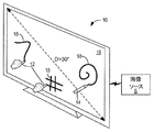
[0015] 図1は、本開示の一実施形態による大型のマルチタッチ表示装置10を示す図である。表示装置10は、通常は、30インチ超の対角線寸法を有する。いくつかの特に大型の形態では、この対角線寸法は、55インチ以上になることもある。表示装置10は、通常は、ユーザの指12またはスタイラス14の複数回の接触(マルチタッチ)を感知するように構成される。表示装置10は、外部コンピュータまたは搭載プロセッサなどの画像ソースSに接続することができる。画像ソースSは、表示装置からマルチタッチ入力を受け取り、このマルチタッチ入力を処理し、表示装置10に表示する適切なグラフィック出力18を生成することができる。画像ソースSについては、図6を参照して以下でさらに詳細に述べる。
FIG. 1 is a diagram illustrating a large
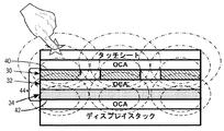
[0016] 図1に示すように、マルチタッチ感知機能を使用可能にするために、表示装置10は、容量性タッチセンシティブディスプレイ16を備える。図2は、容量性タッチセンシティブディスプレイ16の光学スタックの部分的な断面を示す概略図である。図示のように、ディスプレイ16は、指またはスタイラスの接触を受ける上面22を有するプラスチック製の光学用透明タッチシート20と、タッチシート20の底面をタッチセンサ26の上面に接合する光学用透明接着剤層24とを含む。当業者なら、光学用透明接着剤が、入射する可視光を実質的に全て(例えば約99%)透過する種類の接着剤を指すことを理解するであろう。
As shown in FIG. 1, in order to enable the multi-touch sensing function, the
[0017] 図3を参照して以下で詳細に述べるように、タッチセンサ26は、タッチシートの下に離間して配置された複数の電極で構成されたキャパシタのマトリクスを備える。これらの電極は、受信電極層30および送信電極層34に形成される。通常は、これらの電極は、例えば薄膜として堆積させた一様な金属シートを化学エッチングする、触媒インクを誘電体基板に塗布して、その後インクが付着した部分を金属メッキするようにこの基板を処理する添加プロセスを用いる、あるいは誘電体接着剤基板中に金属ワイヤ(例えば、直径が3〜15マイクロメートルのほぼ円形の断面を有する金属ワイヤなど)を配置するなどの手段によって製造される金属導体を含む。透明導電性酸化物(TCO)は、通常は電極では使用されないが、電極の一部を形成するためにTCOを部分的に使用し、他の部分は金属で構成することもできる。一例では、電極は、ほぼ一定の断面を有する薄い金属とすることができ、ディスプレイを見ている人から見て光学的に目立たないような大きさにすることができる。
[0017] As described in detail below with reference to FIG. 3, the
[0018] 受信電極層30と送信電極層34は、別の光学用透明接着剤層32によって互いに接合される。指の接触を検出するために、各行は、通常は、時間変動電圧で連続的に駆動され、各列は、接地電圧に保持される。ある軸を行と指定し、別の軸を列と指定するのは任意であり、これらの軸は、90°以外の角度で交差していてもよい。電極は、ユーザの指またはスタイラスが上面に接触したのに応答して、マトリクス中のキャパシタのうちの少なくとも1つの容量の変化を示すように構成される。検出回路は、時間変動電圧が印加される際に、この容量の変化を検出するように構成され、検出のタイミング、ならびに測定した電流の減衰および/または位相ずれの程度に基づいて、被試験容量を推定することができ、また検出した接触の行および列を特定することができる。電極の構造については、図3および図4を参照して以下でさらに詳細に述べる。
The
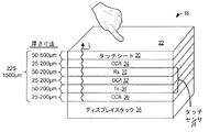
[0019] 図2を参照すると、液晶ディスプレイ(LCD)スタック、有機発光ダイオード(OLED)スタック、プラズマディスプレイパネル(PDP)またはその他のフラットパネルディスプレイスタックなどの発光ディスプレイスタック38は、キャパシタのマトリクスの下に配置される。光学用透明接着剤層36が、キャパシタのマトリクスの底面を、ディスプレイスタック38の上面に接合する。ディスプレイスタック38は、発出された光が光学用透明接着剤層36、タッチセンサ26の受信電極層30および送信電極層34のキャパシタのマトリクス、光学用透明接着剤層32、光学用透明接着剤層24およびタッチシート20を通って発光方向に進行するように、ディスプレイスタック38の上面を通して光Lを発出するように構成される。このようにして、ユーザには、この光が、タッチシート20の上面22に表示された画像のように見える。
[0019] Referring to FIG. 2, a light emitting display stack 38, such as a liquid crystal display (LCD) stack, an organic light emitting diode (OLED) stack, a plasma display panel (PDP) or other flat panel display stack, is under a matrix of capacitors. Placed in. An optical transparent
[0020] 次に、ディスプレイ16の光学スタックの幾何学的形状について述べる。タッチシート20の厚さは、通常は、約50〜500マイクロメートルであり、いくつかの実施形態では115〜135マイクロメートルであり、1つの例示的な実施形態では、125マイクロメートルである。これらの範囲は、望ましくない視差効果を回避できるだけの薄さでありながら、タッチセンサ電極とユーザの指またはスタイラスとの間に十分な誘電体材料を配置して所望の摩擦および摩耗特性をもたらすことが分かっている。
[0020] Next, the geometric shape of the optical stack of the
[0021] 通常は、光学用透明接着剤層24、32および36はそれぞれ、約25〜200マイクロメートルの厚さを有する。この厚さの範囲は、光学スタックの大きさを小さく維持しながら、十分な接着性をもたらすものである。
[0021] Typically, the optical transparent
[0022] タッチシートの上面とディスプレイスタック38の上面の間の厚さ方向の距離は、通常は約225〜1500マイクロメートルである。別の実施形態では、タッチシートの上面とディスプレイスタック38の上面との間の厚さは、約300〜1125マイクロメートルである。これらの範囲の厚さでは、光学スタックを小型の構成にすることができ、望ましくない視差効果がもたらされることが回避しながら、同時に、ディスプレイスタック38からタッチ感知機能への電気的な干渉を生じることなく、タッチセンサの電極が機能できるだけの十分なスペースが得られる。 [0022] The distance in the thickness direction between the top surface of the touch sheet and the top surface of the display stack 38 is typically about 225 to 1500 micrometers. In another embodiment, the thickness between the top surface of the touch sheet and the top surface of the display stack 38 is about 300-1125 micrometers. With thicknesses in these ranges, the optical stack can be configured in a compact configuration, while at the same time causing electrical interference from the display stack 38 to the touch sensing function while avoiding undesirable parallax effects. In this case, a sufficient space for the electrodes of the touch sensor to function can be obtained.
[0023] 図3に示すように、受信電極層30は、複数列に配列された複数の受信電極40を含み、送信電極層34は、複数行に配列された複数の送信電極42を含む。図4の断面に示すように、光学用透明接着剤層32は、受信電極層30と送信電極層34との中間に配置された誘電体層を形成する。各キャパシタ44は、受信電極層30の各受信電極40と送信電極層34の各送信電極42の間の交差領域に形成される。
As shown in FIG. 3, the
[0024] 図2に示すように、受信電極層の厚さは、通常は、約50〜200マイクロメートルであり、送信層の厚さも、通常は、約50〜200マイクロメートルである。表示装置10と同様に、タッチシート20、タッチセンサ26、ディスプレイスタック38、ならびに光学用透明接着剤層24、32および36はそれぞれ、通常は、30インチ以上の対角線寸法を有し、いくつかの実施形態では、55インチ以上の対角線寸法を有する。
[0024] As shown in FIG. 2, the thickness of the receiving electrode layer is usually about 50 to 200 micrometers, and the thickness of the transmitting layer is also usually about 50 to 200 micrometers. Similar to the
[0025] マトリクス中の列を構成する受信電極40および行を構成する送信電極42は、ディスプレイスタック38中の電極と、ディスプレイスタック上面の上方のマトリクス中のキャパシタによって生成される電界との間の電気的な干渉を防止するように、十分に精細なピッチで離間している。通常は、この干渉は、キャパシタの全容量に対する指の接触によるキャパシタの容量の変化の比を1:10〜8:10にするのに十分な程度、またいくつかの実施形態では約3:10にするのに十分な程度に防止される。これを実現するために、行および列の両方の電極を構成する導体のピッチは、3.5mm以上に精細にし、いくつかの実施形態では、2〜3.5mm、他の実施形態では約3mmとする。
[0025] The receive
[0026] このマトリクスは、さらに、複数の隣接する受信電極40を電気的に接続して1つの受信電極グループ48にする導体である、複数の受信連結構造46を含む。このマトリクスは、さらに、複数の隣接する送信電極42を電気的に接続して1つの送信電極グループ52にする導体である、複数の送信連結構造50も含む。このように受信連結構造46および送信連結構造50を使用することにより、受信電極グループと送信電極グループの間の交差領域54の有効容量は、受信電極と送信電極が一体化され、各キャパシタ44の容量が独立している構造と比較して、約4倍に高める。図3では連結構造ごとに2つの電極を示しているが、各受信連結構造46および各送信連結構造50は、3つ以上の対応する受信電極または送信電極を含むこともでき、その場合には、受信電極グループと送信電極グループの間の交差領域54の有効容量は、さらに高まることになることは理解されるであろう。さらに、必要に応じて、連結構造あたりの電極数は、受信電極層と送信電極層とで異なっていてもよいし、各層内で異なっていてもよい。図示のように、行状の送信電極グループおよび列状の受信電極グループのピッチは、通常は7mmより精細であり、いくつかの実施形態では4〜7mm、他の実施形態では約6mmである。これらの範囲のピッチであれば、タッチセンサ26の十分な感知解像度が得られる。上述のように、電極グループ内の各電極を形成する個々の導体(例えば図3に横線および縦線で示す金属導体など)のピッチは、3.5mm以上の精細さであり、いくつかの実施形態では図3に示すように2〜3.5mm、他の実施形態では約3mmである。これらの範囲のピッチであれば、ディスプレイスタック38によって引き起こされる可能性のある電気的干渉に対する十分な遮蔽が得られる。受信電極のピッチと送信電極のピッチは、図3では同じものとして示しているが、いくつかの実施形態では、上記の範囲内の異なるピッチをそれぞれに対して使用してもよいことは理解されるであろう。
The matrix further includes a plurality of receiving connection structures 46 that are conductors that electrically connect a plurality of adjacent receiving
[0027] 駆動回路60は、送信機62を介して各送信電極グループに時間変動電圧を連続的に駆動するために設けられ、検出回路64は、受信機66を介して電流の変化を感知するために設けられる。指またはスタイラスの接触に対応する各キャパシタまたは各キャパシタグループの容量の変化は、検出回路が検出する電流の変化から推測される。これらの変化のタイミングならびに受信した電流信号の位相ずれおよび/または減衰に基づいて、指の接触があった行および列が決定される。
A
[0028] 図4に示すように、上述のタッチセンサ26の電極の構造によって、タッチ表面の領域において、各キャパシタ44の電界(一点鎖線で示す)を、普通ならディスプレイスタック38によって生じる望ましくない電気的干渉(破線で示す)から効果的に遮蔽することができる。その結果として、上述の薄い寸法を有するスタックで構成されたディスプレイ16でも、ユーザのスタイラスまたは指の接触(星印で示す)が、上述の範囲内のキャパシタ44の全容量に対する容量の変化を適切に引き起こすことができ、表示装置が表示表面上の接触を適切に感知することができるようになる。
As shown in FIG. 4, due to the electrode structure of the
[0029] さらに、硬いガラス製タッチ表面の代わりにプラスチック製タッチシートを使用することにより、中間層を介したガラスとディスプレイスタックの剛性材料/剛性材料の接合による積層歪みに関連する問題が回避され、この歪みを吸収するために光学用透明接着剤の厚い歪み吸収層を設ける必要がない。その代わりに、上述の寸法の薄い層を、光学用透明接着剤層36として使用することができる。さらに、上述の構成は、タッチ表面としてガラスを用いる従来の大型の容量性タッチセンシティブディスプレイより製造コストが安い。
[0029] Further, by using a plastic touch sheet instead of a hard glass touch surface, problems associated with stacking distortion due to the bonding of the glass to the rigid / rigid material of the display stack via an intermediate layer are avoided. In order to absorb this strain, there is no need to provide a thick strain absorbing layer of the optical transparent adhesive. Alternatively, a thin layer with the dimensions described above can be used as the optical transparent
[0030] 次に図5を参照して、本開示の一実施形態による容量性タッチセンシティブ表示装置を製造する方法100について説明する。方法100は、ディスプレイスタックの上面を通して光を発出するように構成されたディスプレイスタックを提供する工程102を含む。上述のように、LCDスタック、OLEDスタック、PDPスタック、またはその他のフラットパネルディスプレイスタックを、方法100のディスプレイスタックとして使用することができる。この方法は、ディスプレイスタックの上面の上に第1の光学用透明接着剤層を積層する工程104と、第1の接着剤層の上方に位置決めされた金属導体を含む電極で構成されたキャパシタのマトリクスを有するタッチセンサを積層する工程106とを含む。この方法は、キャパシタのマトリクスの上方に第2の光学用透明接着剤層を積層する工程108と、第2の接着剤層の上方にタッチシートを積層する工程110とを含む。キャパシタのマトリクスは、ユーザの指またはスタイラスがタッチシートの上面に接触したのに応答して、それらのキャパシタのうちの少なくとも1つの容量の変化を示すように構成される。
Next, with reference to FIG. 5, a
[0031] 方法100で形成される各層の寸法は、以下の通りである。通常は、タッチシートの上面とディスプレイスタックの上面との間の距離は、約225〜1500マイクロメートルであり、300〜1125マイクロメートルとすることができる。タッチシートの厚さは、通常は、約50〜500マイクロメートルである。第1の光学用透明接着剤層および第2の光学用透明接着剤層はそれぞれ、約25〜200マイクロメートルの厚さを有することができる。これらの厚さ寸法の利点については、上記で詳細に述べた。タッチシート、タッチセンサおよびディスプレイスタックはそれぞれ、30インチ以上の対角線寸法を有し、いくつかの実施形態では55インチ以上の対角線寸法を有する。
[0031] The dimensions of each layer formed by
[0032] 工程106で積層されるタッチセンサは、工程106Aで、列状に配列された複数の受信電極を含む受信電極層を形成し、工程106Bで、行状に配列された複数の送信電極を含む送信電極層を形成し、工程106Cで、受信層と送信層の中間に位置決めされた誘電体層を形成することによって、形成することができる。このようにして、各キャパシタは、受信層の各電極と送信層の各電極の間の交差領域に形成される。通常は、受信電極層および送信電極層はそれぞれ、約50〜200マイクロメートルの厚さを有し、電極は、金属導体を含む。金属導体の断面は、その長さに沿って一定であってもよいし、変化してもよい。
The touch sensor stacked in
[0033] タッチセンサのマトリクス中の列を構成する受信電極および行を構成する送信電極は、ディスプレイスタック中の電極とディスプレイスタック上面の上方のマトリクス中のキャパシタが生成する電界との間の電気的な干渉を防止するように、十分に精細なピッチで離間している。この干渉は、キャパシタの全容量に対する指の接触によるキャパシタの容量の変化の比を1:10〜8:10にするのに十分な程度、またいくつかの実施形態では約3:10にするのに十分な程度に防止される。これらの比であれば、ノイズを除去するために費用および時間のかかるデジタル信号処理を行わなくても、検出回路が信号を明確に読み取ることができる。これを実現するために、電極を構成する導体のピッチは、3.5mm以上に精細に設定することができ、いくつかの実施形態では、2〜3.5mmに設定することができ、他の実施形態では約3mmに設定することができ、電極グループのピッチは、7mmより精細に設定することができ、いくつかの実施形態では4〜7ミリメートルに設定することができ、1実施形態では6ミリメートルに設定することができる。これらのピッチ範囲は、十分な干渉の遮蔽、および十分な接触感知の解像度をもたらす。ピッチを4ミリメートルより精細にすることも可能ではあるが、4ミリメートルより精細にしても、指の接触感知の解像度および精度に関して、性能の上積みはほとんどない。ピッチが7ミリメートルを超えると、表示装置の指の接触位置の精度が低下する傾向がある。 [0033] The receiving electrodes constituting the columns in the matrix of the touch sensor and the transmitting electrodes constituting the rows are electrically connected between the electrodes in the display stack and the electric field generated by the capacitors in the matrix above the upper surface of the display stack. Are separated with a sufficiently fine pitch to prevent unwanted interference. This interference is sufficient to make the ratio of the change in capacitance of the capacitor due to finger contact to the total capacitance of the capacitor 1: 10-8: 10, and in some embodiments about 3:10. Is sufficiently prevented. With these ratios, the detection circuit can clearly read the signal without performing expensive and time-consuming digital signal processing to remove noise. To achieve this, the pitch of the conductors that make up the electrodes can be set finely to 3.5 mm or more, and in some embodiments can be set to 2 to 3.5 mm, other In embodiments, it can be set to about 3 mm, and the pitch of the electrode groups can be set more finely than 7 mm, in some embodiments it can be set to 4-7 millimeters, and in one embodiment 6 Can be set to millimeters. These pitch ranges provide sufficient interference shielding and sufficient touch sensing resolution. Although it is possible to make the pitch finer than 4 millimeters, there is little performance gain in terms of resolution and accuracy of finger touch sensing. When the pitch exceeds 7 mm, the accuracy of the contact position of the finger of the display device tends to be lowered.
[0034] 方法100は、複数の隣接する受信電極を電気的に接続して1つの受信電極グループにする複数の受信連結構造を含み、さらに複数の隣接する送信電極を電気的に接続して1つの送信電極グループにする複数の送信連結構造を含み、それにより受信電極グループと送信電極グループの間の交差領域の有効容量を、受信電極と送信電極が一体化された構造と比較して少なくとも約4倍に高めるようにマトリクスを形成する工程106Dをさらに含むことができる。
[0034] The
[0035] 上述の方法では、タッチセンサをディスプレイスタックによる電気的干渉から遮蔽して、正確な接触感知を可能にしながら、同時に従来の大型の容量性タッチセンシティブ表示装置と比較してコスト面の利点をもたらす、大型の容量性タッチセンシティブ表示装置を製造することができる。 [0035] The above-described method shields the touch sensor from electrical interference by the display stack and enables accurate touch sensing, while at the same time providing a cost advantage compared to a conventional large capacitive touch sensitive display device. A large capacitive touch-sensitive display device can be manufactured.
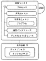
[0036] 図6は、本発明の一実施形態による例示的な画像ソースSを示す図である。上述のように、画像ソースSは、サーバ、ラップトップコンピューティングデバイス、セットトップボックス、ゲームコンソール、デスクトップコンピュータ、タブレットコンピューティングデバイス、携帯電話、またはその他の適当なコンピューティングデバイスなど、外部のコンピューティングデバイスとすることができる。あるいは、画像ソースSは、表示装置10内に一体化してもよい。
[0036] FIG. 6 is a diagram illustrating an exemplary image source S according to one embodiment of the invention. As described above, the image source S can be external computing such as a server, laptop computing device, set-top box, game console, desktop computer, tablet computing device, mobile phone, or other suitable computing device. It can be a device. Alternatively, the image source S may be integrated in the
[0037] 画像ソースSは、プロセッサ、揮発性メモリ、およびソフトウェアプログラムを不揮発的に記憶するように構成された大容量記憶装置などの不揮発性メモリを含む。記憶されたプログラムは、揮発性メモリの一部分を用いてプロセッサによって実行される。プログラムのための入力は、表示装置10のディスプレイ16と一体化されたタッチセンサ26など、様々なユーザ入力装置を介して受信することができる。この入力は、プログラムによって処理することができ、適当なグラフィック出力を、ディスプレイインタフェースを介して表示装置10に送信して、ユーザに対して表示することができる。
[0037] The image source S includes a processor, volatile memory, and non-volatile memory such as a mass storage device configured to store software programs in a non-volatile manner. The stored program is executed by the processor using a portion of the volatile memory. Input for the program can be received via various user input devices, such as a
[0038] プロセッサ、揮発性メモリ、および不揮発性メモリは、別個の構成要素として構成してもよいし、例えばチップ上の1つのシステムとして一体化してもよい。さらに、プロセッサは、中央処理装置、マルチコアプロセッサ、ASIC、システムオンチップ、またはその他のタイプのプロセッサとすることができる。いくつかの実施形態では、プロセッサ、揮発性メモリ、および不揮発性メモリの特徴を、例えばフィールドプログラマブルゲートアレイ(FPGA)、特定用途プログラム向け集積回路/特定用途向け集積回路(PASIC/ASIC)、特定プログラム向け標準品/特定用途向け標準品(PSSP/ASSP)、システムオンチップ(SOC)システム、複合プログラマブル論理デバイス(CPLD)などの装置に一体化することもできる。 [0038] The processor, volatile memory, and non-volatile memory may be configured as separate components or may be integrated, for example, as one system on a chip. Further, the processor may be a central processing unit, multi-core processor, ASIC, system on chip, or other type of processor. In some embodiments, the features of the processor, volatile memory, and non-volatile memory may include, for example, a field programmable gate array (FPGA), an application specific integrated circuit / application specific integrated circuit (PAASIC / ASIC), a specific program It can also be integrated into devices such as standard products for specific use / standard products for specific applications (PSSP / ASSP), system-on-chip (SOC) systems, composite programmable logic devices (CPLD).
[0039] 通信インタフェースを設けて、インターネットなどのローカルエリアネットワーク接続および広域ネットワーク接続を介してサーバなどの他のコンピューティングデバイスと通信することもできる。 [0039] A communication interface may also be provided to communicate with other computing devices such as servers via local area network connections such as the Internet and wide area network connections.
[0040] 不揮発性メモリは、取外し可能媒体および/または組込みデバイスを含むことができる。例えば、不揮発性メモリとしては、特に、光学メモリデバイス(例えばCD、DVD、HD−DVD、Blu−Rayディスクなど)、半導体メモリデバイス(例えばフラッシュ、EPROM、EEPROMなど)、および/または磁気メモリデバイス(例えばハードディスクドライブ、フロッピーディスクドライブ、テープドライブ、MRAMなど)などを含むことができる。 [0040] Non-volatile memory may include removable media and / or embedded devices. For example, non-volatile memory includes, among others, optical memory devices (eg, CD, DVD, HD-DVD, Blu-Ray disc, etc.), semiconductor memory devices (eg, flash, EPROM, EEPROM, etc.), and / or magnetic memory devices (eg, For example, a hard disk drive, floppy disk drive, tape drive, MRAM, etc.) can be included.
[0041] 本明細書に記載する方法およびプロセスを実施するために実行可能なデータおよび/または命令を記憶するために使用することができる、取外し可能なコンピュータ可読記憶媒体(CRSM)を設けることもできる。取外し可能なコンピュータ可読記憶媒体は、特に、CD、DVD、HD−DVD、Blu−Rayディスク、EEPROM、および/またはフロッピーディスクの形態をとることができる。 [0041] A removable computer readable storage medium (CRSM) may also be provided that can be used to store executable data and / or instructions to perform the methods and processes described herein. it can. Removable computer readable storage media can take the form of CDs, DVDs, HD-DVDs, Blu-Ray disks, EEPROMs, and / or floppy disks, among others.
[0042] 不揮発性メモリおよびCRSMは、通常は、画像ソースの電源が切られても一定時間命令を保持するように構成された物理的デバイスであるが、いくつかの実施形態では、本明細書に記載する命令の特徴は、図示の通信バスなどのコンピュータ可読通信媒体を介して、少なくとも限られた時間の間は、物理的デバイスによって保持されない純粋な信号(例えば電磁気信号、光信号など)によって一時的に伝搬することができる。 [0042] Non-volatile memory and CRSM are typically physical devices that are configured to retain instructions for a period of time even when the image source is turned off. Are characterized by pure signals (eg, electromagnetic signals, optical signals, etc.) that are not held by the physical device for at least a limited time via a computer-readable communication medium such as the illustrated communication bus. Can be temporarily propagated.
[0043] 「プログラム」という用語は、1つまたは複数の特定の機能を実行するために実施されるシステムのソフトウェアファームウェアなどを述べるために使用することができる。場合によっては、このようなプログラムは、不揮発性メモリに保持される命令を揮発性メモリの一部分を用いてプログラムが実行することによってインスタンス化することができる。同じアプリケーション、サービス、コードブロック、オブジェクト、ライブラリ、ルーチン、API、機能などから異なるプログラムをインスタンス化することができることを理解されたい。同様に、異なるアプリケーション、サービス、コードブロック、オブジェクト、ルーチン、API、機能などから同じプログラムをインスタンス化することができる。「プログラム」という用語は、個々の実行可能なファイル、データファイル、ライブラリ、ドライバ、スクリプト、データベースレコードなど、またはそれらのグループを包含するものとする。 [0043] The term "program" can be used to describe the software firmware of a system that is implemented to perform one or more specific functions. In some cases, such a program can be instantiated by causing the program to execute instructions held in non-volatile memory using a portion of volatile memory. It should be understood that different programs can be instantiated from the same application, service, code block, object, library, routine, API, function, etc. Similarly, the same program can be instantiated from different applications, services, code blocks, objects, routines, APIs, functions, and the like. The term “program” is intended to encompass individual executable files, data files, libraries, drivers, scripts, database records, etc., or groups thereof.
[0044] 本明細書に記載する構成および/または手法は本質的に例示であること、ならびに上記の具体的な実施形態または例は、多数の変形が可能であるので、限定的な意味で考慮すべきものではないことを理解されたい。上述の実施形態、および図面に示す実施形態は、様々なデバイスの例として用いるものである。本開示の主題は、本明細書に開示する様々な構成、特徴、機能、および/または性質の、全ての新規な自明でない組合せおよび部分的組合せ、ならびにそれらのあらゆる均等物を含む。 [0044] The configurations and / or techniques described herein are exemplary in nature, and the specific embodiments or examples described above are contemplated in a limiting sense since numerous variations are possible. Please understand that it should not be. The above-described embodiments and the embodiments shown in the drawings are used as examples of various devices. The subject matter of this disclosure includes all novel non-obvious combinations and subcombinations of the various configurations, features, functions, and / or properties disclosed herein, and any equivalents thereof.
Claims (10)
前記タッチシートの下に位置し、金属導体を含む電極で構成されたキャパシタのマトリクスを有するタッチセンサであって、ユーザの指またはスタイラスが前記上面に接触したのに応答して前記キャパシタのうちの少なくとも1つの容量の変化を示すように構成されたタッチセンサと、
キャパシタの前記マトリクスの下に位置するディスプレイスタックであって、前記ディスプレイスタックの上面を通して、前記タッチセンサおよび前記タッチシートを通って発光方向に進行するように光を発出するように構成されたディスプレイスタックとを備え、
前記タッチシートの前記上面と前記ディスプレイスタックの前記上面との間の距離が、約225〜1500マイクロメートルである、容量性タッチセンシティブ表示装置。 A touch sheet having an upper surface;
A touch sensor having a matrix of capacitors, which is located under the touch sheet and is composed of electrodes including metal conductors, the touch sensor being in response to a user's finger or stylus touching the top surface. A touch sensor configured to indicate a change in at least one capacitance;
A display stack located below the matrix of capacitors, the display stack configured to emit light to travel in a light emitting direction through the top surface of the display stack, through the touch sensor and the touch sheet. And
A capacitive touch-sensitive display device, wherein a distance between the top surface of the touch sheet and the top surface of the display stack is about 225 to 1500 micrometers.
前記第1の光学用透明接着剤層の厚さが、約25〜200マイクロメートルである、請求項1に記載の容量性タッチセンシティブ表示装置。 A first optical transparent adhesive layer that joins the bottom surface of the touch sensor to the top surface of the display stack;
The capacitive touch-sensitive display device according to claim 1, wherein the thickness of the first optical transparent adhesive layer is about 25 to 200 micrometers.
前記第2の光学用透明接着剤層の厚さが、約25〜200マイクロメートルである、請求項3に記載の容量性タッチセンシティブ表示装置。 A second optical transparent adhesive layer that joins the bottom surface of the touch sheet to the top surface of the touch sensor;
The capacitive touch-sensitive display device according to claim 3, wherein the thickness of the second optical transparent adhesive layer is about 25 to 200 micrometers.
列状に配列された複数の受信電極を含む受信電極層と、
行状に配列された複数の送信電極を含む送信電極層と、
前記受信電極層と前記送信電極層の中間に位置する誘電体層とを含み、
各キャパシタが、前記受信電極層の各電極と前記送信電極層の各電極の間の交差領域に形成される、請求項1に記載の容量性タッチセンシティブ表示装置。 The touch sensor is
A receiving electrode layer including a plurality of receiving electrodes arranged in a row;
A transmission electrode layer comprising a plurality of transmission electrodes arranged in rows;
A dielectric layer positioned between the receiving electrode layer and the transmitting electrode layer;
The capacitive touch-sensitive display device according to claim 1, wherein each capacitor is formed in a crossing region between each electrode of the receiving electrode layer and each electrode of the transmitting electrode layer.
前記送信電極層の厚さが、約50〜200マイクロメートルである、請求項5に記載の容量性タッチセンシティブ表示装置。 The receiving electrode layer has a thickness of about 50 to 200 micrometers;
The capacitive touch-sensitive display device according to claim 5, wherein the thickness of the transmission electrode layer is about 50 to 200 micrometers.
Applications Claiming Priority (3)
| Application Number | Priority Date | Filing Date | Title |
|---|---|---|---|
| US13/735,958 US9250753B2 (en) | 2013-01-07 | 2013-01-07 | Capacitive touch surface in close proximity to display |
| US13/735,958 | 2013-01-07 | ||
| PCT/US2014/010269 WO2014107636A1 (en) | 2013-01-07 | 2014-01-06 | Capacitive touch surface in close proximity to display |
Publications (2)
| Publication Number | Publication Date |
|---|---|
| JP2016505991A true JP2016505991A (en) | 2016-02-25 |
| JP2016505991A5 JP2016505991A5 (en) | 2017-02-02 |
Family
ID=50029244
Family Applications (1)
| Application Number | Title | Priority Date | Filing Date |
|---|---|---|---|
| JP2015551798A Pending JP2016505991A (en) | 2013-01-07 | 2014-01-06 | Capacitive touch surface in the vicinity of the display |
Country Status (7)
| Country | Link |
|---|---|
| US (1) | US9250753B2 (en) |
| EP (1) | EP2941681B1 (en) |
| JP (1) | JP2016505991A (en) |
| KR (1) | KR102321946B1 (en) |
| CN (1) | CN105074632B (en) |
| TW (1) | TWI601050B (en) |
| WO (1) | WO2014107636A1 (en) |
Families Citing this family (28)
| Publication number | Priority date | Publication date | Assignee | Title |
|---|---|---|---|---|
| CN103412667B (en) * | 2013-04-12 | 2015-04-08 | 深圳欧菲光科技股份有限公司 | Touch panel and touch display device |
| KR20150043787A (en) * | 2013-10-15 | 2015-04-23 | 삼성전기주식회사 | Touch screen panel and manufacturing method thereof |
| GB2520050A (en) * | 2013-11-08 | 2015-05-13 | Nokia Technologies Oy | An apparatus |
| TWI567600B (en) * | 2013-11-26 | 2017-01-21 | 恆顥科技股份有限公司 | Touch apparatus |
| JP5990205B2 (en) * | 2014-02-19 | 2016-09-07 | 富士フイルム株式会社 | Laminated structure and touch panel module |
| US9176633B2 (en) * | 2014-03-31 | 2015-11-03 | Synaptics Incorporated | Sensor device and method for estimating noise in a capacitive sensing device |
| US10411078B2 (en) * | 2014-04-14 | 2019-09-10 | Industrial Technology Research Institute | Sensing display apparatus |
| TWM505004U (en) * | 2014-04-14 | 2015-07-11 | Ind Tech Res Inst | Touch panel |
| TWI613580B (en) * | 2017-01-25 | 2018-02-01 | 財團法人工業技術研究院 | Sensing display apparatus |
| US9558390B2 (en) * | 2014-07-25 | 2017-01-31 | Qualcomm Incorporated | High-resolution electric field sensor in cover glass |
| JP6275618B2 (en) * | 2014-10-15 | 2018-02-07 | 富士フイルム株式会社 | Conductive film, display device including the same, and method for evaluating wiring pattern of conductive film |
| TWI559187B (en) * | 2015-01-16 | 2016-11-21 | Composite touch buttons and their modules | |
| CN104656987A (en) * | 2015-01-21 | 2015-05-27 | 业成光电(深圳)有限公司 | Transparent conductive structure with metal grid |
| CN104699310A (en) * | 2015-03-31 | 2015-06-10 | 合肥京东方光电科技有限公司 | Touch screen and manufacturing method thereof |
| US9946397B2 (en) * | 2015-06-15 | 2018-04-17 | Microchip Technology Incorporated | Sensor design for enhanced touch and gesture decoding |
| CN106708336B (en) * | 2015-07-14 | 2020-08-25 | 比亚迪股份有限公司 | Capacitive touch screen |
| WO2017031687A1 (en) * | 2015-08-25 | 2017-03-02 | 华为技术有限公司 | Terminal |
| US9983753B2 (en) * | 2015-10-01 | 2018-05-29 | Bidirectional Display Inc. | Optical-capacitive sensor panel device and method for manufacturing same |
| US20170108959A1 (en) * | 2015-10-15 | 2017-04-20 | Richard Keith McMillan | Two piece lens assembly |
| KR102489262B1 (en) * | 2016-01-13 | 2023-01-18 | 삼성디스플레이 주식회사 | Touch screen panel and method of manufacturing the same |
| US10019122B2 (en) | 2016-03-31 | 2018-07-10 | Synaptics Incorporated | Capacitive sensing using non-integer excitation |
| RU2731338C1 (en) * | 2016-09-21 | 2020-09-01 | Конинклейке Филипс Н.В. | Mirror device with capacitive touch screen and method of manufacturing thereof |
| US10507385B2 (en) | 2017-01-25 | 2019-12-17 | Kieran S. Lyden | Game controller |
| GB2559575B (en) * | 2017-02-09 | 2020-02-26 | Solomon Systech Ltd | Touch sensor |
| CN107741798A (en) * | 2017-11-23 | 2018-02-27 | 深圳达沃斯光电有限公司 | It is a kind of that aobvious all-in-one and its data output method are touched based on large scale capacitance plate |
| US10671227B2 (en) | 2018-08-13 | 2020-06-02 | Dell Products L.P. | Information handling system narrow bezel touchscreen display touch detection grid |
| KR20220011260A (en) * | 2020-07-20 | 2022-01-28 | 삼성디스플레이 주식회사 | Display device |
| KR102510516B1 (en) * | 2021-02-10 | 2023-03-14 | 동우 화인켐 주식회사 | Digitizer and image display device including the same |
Citations (8)
| Publication number | Priority date | Publication date | Assignee | Title |
|---|---|---|---|---|
| JP2010170515A (en) * | 2008-12-26 | 2010-08-05 | Sony Corp | Touch panel, display device and electronic device |
| JP2011018194A (en) * | 2009-07-09 | 2011-01-27 | Shin Etsu Polymer Co Ltd | Sensor panel for large-size display |
| JP2011128982A (en) * | 2009-12-18 | 2011-06-30 | Wacom Co Ltd | Device and method for detecting pointer |
| JP2012094115A (en) * | 2010-09-30 | 2012-05-17 | Fujifilm Corp | Electrostatic capacitive touch panel |
| JP2012138019A (en) * | 2010-12-27 | 2012-07-19 | Dainippon Printing Co Ltd | Display device with touch panel |
| JP2012226423A (en) * | 2011-04-15 | 2012-11-15 | Panasonic Corp | Touch panel device and plasma display device including the same |
| JP2012230471A (en) * | 2011-04-25 | 2012-11-22 | Japan Display East Co Ltd | Touch panel |
| WO2012161078A1 (en) * | 2011-05-20 | 2012-11-29 | Umeda Masahiro | Printing film for touch panel, cover glass for touch panel, liquid crystal display panel, multi-function terminal, and method for manufacturing printing film for touch panel |
Family Cites Families (34)
| Publication number | Priority date | Publication date | Assignee | Title |
|---|---|---|---|---|
| US7006081B2 (en) | 2000-10-20 | 2006-02-28 | Elo Touchsystems, Inc. | Acoustic touch sensor with laminated substrate |
| US7009663B2 (en) | 2003-12-17 | 2006-03-07 | Planar Systems, Inc. | Integrated optical light sensitive active matrix liquid crystal display |
| US7129935B2 (en) | 2003-06-02 | 2006-10-31 | Synaptics Incorporated | Sensor patterns for a capacitive sensing apparatus |
| US7165323B2 (en) * | 2003-07-03 | 2007-01-23 | Donnelly Corporation | Method of manufacturing a touch screen |
| US7339579B2 (en) | 2003-12-15 | 2008-03-04 | 3M Innovative Properties Company | Wiring harness and touch sensor incorporating same |
| US7567240B2 (en) | 2005-05-31 | 2009-07-28 | 3M Innovative Properties Company | Detection of and compensation for stray capacitance in capacitive touch sensors |
| GB2428306B (en) | 2005-07-08 | 2007-09-26 | Harald Philipp | Two-dimensional capacitive position sensor |
| US8269744B2 (en) | 2008-09-05 | 2012-09-18 | Mitsubishi Electric Corporation | Touch screen, touch panel and display device |
| JP2010097070A (en) * | 2008-10-17 | 2010-04-30 | Nitto Denko Corp | Transparent pressure-sensitive adhesive sheet for flat panel display, and flat panel display |
| US9244568B2 (en) | 2008-11-15 | 2016-01-26 | Atmel Corporation | Touch screen sensor |
| TWI373665B (en) * | 2008-12-25 | 2012-10-01 | Au Optronics Corp | Touch panel structure |
| US20100214247A1 (en) | 2009-02-20 | 2010-08-26 | Acrosense Technology Co., Ltd. | Capacitive Touch Panel |
| US20100218100A1 (en) * | 2009-02-25 | 2010-08-26 | HNTB Holdings, Ltd. | Presentation system |
| WO2010099132A2 (en) | 2009-02-26 | 2010-09-02 | 3M Innovative Properties Company | Touch screen sensor and patterned substrate having overlaid micropatterns with low visibility |
| US8278571B2 (en) | 2009-04-03 | 2012-10-02 | Pixart Imaging Inc. | Capacitive touchscreen or touchpad for finger and active stylus |
| CN101907922B (en) | 2009-06-04 | 2015-02-04 | 新励科技(深圳)有限公司 | Touch and touch control system |
| US8310457B2 (en) | 2009-06-30 | 2012-11-13 | Research In Motion Limited | Portable electronic device including tactile touch-sensitive input device and method of protecting same |
| CN102043184B (en) * | 2009-10-09 | 2013-10-09 | Lg化学株式会社 | Integrated touch polarizer and touch panel comprising the same |
| US8599150B2 (en) * | 2009-10-29 | 2013-12-03 | Atmel Corporation | Touchscreen electrode configuration |
| JP5601944B2 (en) * | 2010-06-28 | 2014-10-08 | 帝人株式会社 | Touch panel device and display device with touch panel device |
| US8766931B2 (en) | 2010-07-16 | 2014-07-01 | Perceptive Pixel Inc. | Capacitive touch sensor having code-divided and time-divided transmit waveforms |
| KR101560069B1 (en) | 2010-08-27 | 2015-10-26 | 유아이씨오, 인크. | Capacitive touch screen having dynamic capacitance control and improved touch-sensing |
| JP5514674B2 (en) | 2010-08-31 | 2014-06-04 | 富士フイルム株式会社 | Conductive sheet, method of using conductive sheet, and capacitive touch panel |
| US9252768B2 (en) * | 2010-09-13 | 2016-02-02 | Atmel Corporation | Position-sensing panel |
| KR101704536B1 (en) | 2010-10-08 | 2017-02-09 | 삼성전자주식회사 | Touch Panel type of Slim and Portable Device including the same |
| US9007332B2 (en) * | 2011-03-22 | 2015-04-14 | Atmel Corporation | Position sensing panel |
| US8797285B2 (en) | 2011-04-18 | 2014-08-05 | Atmel Corporation | Panel |
| KR101978666B1 (en) * | 2011-06-10 | 2019-05-15 | 미래나노텍(주) | Substrate for Touch Screen Sensor, Touch Screen Sensor and Touch Screen Panel |
| US8780074B2 (en) | 2011-07-06 | 2014-07-15 | Sharp Kabushiki Kaisha | Dual-function transducer for a touch panel |
| US9501179B2 (en) * | 2011-08-04 | 2016-11-22 | Atmel Corporation | Touch sensor for curved or flexible surfaces |
| KR20130027747A (en) | 2011-09-08 | 2013-03-18 | 삼성전기주식회사 | Touch pannel |
| KR101665210B1 (en) | 2011-09-13 | 2016-10-11 | 군제 가부시키가이샤 | Touch panel |
| JP5506758B2 (en) | 2011-10-03 | 2014-05-28 | 三菱電機株式会社 | Touch screen, touch panel, and display device including the same |
| JP5734828B2 (en) | 2011-12-07 | 2015-06-17 | 株式会社タッチパネル研究所 | Structural material for touch panel and touch panel structure |
-
2013
- 2013-01-07 US US13/735,958 patent/US9250753B2/en active Active
-
2014
- 2014-01-06 JP JP2015551798A patent/JP2016505991A/en active Pending
- 2014-01-06 EP EP14701844.4A patent/EP2941681B1/en active Active
- 2014-01-06 CN CN201480004204.0A patent/CN105074632B/en active Active
- 2014-01-06 TW TW103100386A patent/TWI601050B/en active
- 2014-01-06 WO PCT/US2014/010269 patent/WO2014107636A1/en active Application Filing
- 2014-01-06 KR KR1020157020973A patent/KR102321946B1/en active IP Right Grant
Patent Citations (8)
| Publication number | Priority date | Publication date | Assignee | Title |
|---|---|---|---|---|
| JP2010170515A (en) * | 2008-12-26 | 2010-08-05 | Sony Corp | Touch panel, display device and electronic device |
| JP2011018194A (en) * | 2009-07-09 | 2011-01-27 | Shin Etsu Polymer Co Ltd | Sensor panel for large-size display |
| JP2011128982A (en) * | 2009-12-18 | 2011-06-30 | Wacom Co Ltd | Device and method for detecting pointer |
| JP2012094115A (en) * | 2010-09-30 | 2012-05-17 | Fujifilm Corp | Electrostatic capacitive touch panel |
| JP2012138019A (en) * | 2010-12-27 | 2012-07-19 | Dainippon Printing Co Ltd | Display device with touch panel |
| JP2012226423A (en) * | 2011-04-15 | 2012-11-15 | Panasonic Corp | Touch panel device and plasma display device including the same |
| JP2012230471A (en) * | 2011-04-25 | 2012-11-22 | Japan Display East Co Ltd | Touch panel |
| WO2012161078A1 (en) * | 2011-05-20 | 2012-11-29 | Umeda Masahiro | Printing film for touch panel, cover glass for touch panel, liquid crystal display panel, multi-function terminal, and method for manufacturing printing film for touch panel |
Also Published As
| Publication number | Publication date |
|---|---|
| TW201439867A (en) | 2014-10-16 |
| CN105074632A (en) | 2015-11-18 |
| CN105074632B (en) | 2018-12-11 |
| US9250753B2 (en) | 2016-02-02 |
| TWI601050B (en) | 2017-10-01 |
| EP2941681A1 (en) | 2015-11-11 |
| KR102321946B1 (en) | 2021-11-03 |
| KR20150103720A (en) | 2015-09-11 |
| WO2014107636A1 (en) | 2014-07-10 |
| US20140192007A1 (en) | 2014-07-10 |
| EP2941681B1 (en) | 2019-07-24 |
Similar Documents
| Publication | Publication Date | Title |
|---|---|---|
| KR102321946B1 (en) | Capacitive touch surface in close proximity to display | |
| US10216025B2 (en) | Capacitive touch screen and bending judgment method therefor, and display device | |
| US10048819B2 (en) | High resistivity metal fan out | |
| US8576193B2 (en) | Brick layout and stackup for a touch screen | |
| US10095335B2 (en) | In-cell type touch panel and manufacturing method thereof, liquid crystal display device | |
| US8487898B2 (en) | Ground guard for capacitive sensing | |
| US9733508B2 (en) | Touch liquid crystal display device | |
| KR101686539B1 (en) | Touch input device | |
| KR102393947B1 (en) | Merged floating pixels in a touch screen | |
| JP6143587B2 (en) | Touch panel, display device with touch panel | |
| US20140035864A1 (en) | Capacitive touch-control panel and apparatus thereof | |
| US20120098760A1 (en) | Touch sensitive electronic device | |
| US20110100727A1 (en) | Touch Sensitive Device with Dielectric Layer | |
| US10101860B2 (en) | Borderless projected capacitive multitouch sensor | |
| WO2015021617A1 (en) | Single-layered capacitive touch-control unit and capacitive touch screen | |
| US10048812B2 (en) | Monolayer mutual-capacitive touch panel and capacitive touchscreen | |
| US9958996B2 (en) | Capacitive touch sensor | |
| JP2012230471A (en) | Touch panel | |
| KR20160147688A (en) | Touch input device |
Legal Events
| Date | Code | Title | Description |
|---|---|---|---|
| A521 | Request for written amendment filed |
Free format text: JAPANESE INTERMEDIATE CODE: A523 Effective date: 20161209 |
|
| A621 | Written request for application examination |
Free format text: JAPANESE INTERMEDIATE CODE: A621 Effective date: 20161209 |
|
| A131 | Notification of reasons for refusal |
Free format text: JAPANESE INTERMEDIATE CODE: A131 Effective date: 20170921 |
|
| A977 | Report on retrieval |
Free format text: JAPANESE INTERMEDIATE CODE: A971007 Effective date: 20170920 |
|
| A521 | Request for written amendment filed |
Free format text: JAPANESE INTERMEDIATE CODE: A523 Effective date: 20171219 |
|
| A02 | Decision of refusal |
Free format text: JAPANESE INTERMEDIATE CODE: A02 Effective date: 20180219 |