JP2016505157A - Surface-enhanced fluorescence spectrometer - Google Patents
Surface-enhanced fluorescence spectrometer Download PDFInfo
- Publication number
- JP2016505157A JP2016505157A JP2015555973A JP2015555973A JP2016505157A JP 2016505157 A JP2016505157 A JP 2016505157A JP 2015555973 A JP2015555973 A JP 2015555973A JP 2015555973 A JP2015555973 A JP 2015555973A JP 2016505157 A JP2016505157 A JP 2016505157A
- Authority
- JP
- Japan
- Prior art keywords
- ses
- fluorescence
- fluorescent
- elements
- enhancing element
- Prior art date
- Legal status (The legal status is an assumption and is not a legal conclusion. Google has not performed a legal analysis and makes no representation as to the accuracy of the status listed.)
- Pending
Links
Images


Classifications
-
- G—PHYSICS
- G01—MEASURING; TESTING
- G01N—INVESTIGATING OR ANALYSING MATERIALS BY DETERMINING THEIR CHEMICAL OR PHYSICAL PROPERTIES
- G01N21/00—Investigating or analysing materials by the use of optical means, i.e. using sub-millimetre waves, infrared, visible or ultraviolet light
- G01N21/62—Systems in which the material investigated is excited whereby it emits light or causes a change in wavelength of the incident light
- G01N21/63—Systems in which the material investigated is excited whereby it emits light or causes a change in wavelength of the incident light optically excited
- G01N21/64—Fluorescence; Phosphorescence
- G01N21/645—Specially adapted constructive features of fluorimeters
- G01N21/648—Specially adapted constructive features of fluorimeters using evanescent coupling or surface plasmon coupling for the excitation of fluorescence
-
- B—PERFORMING OPERATIONS; TRANSPORTING
- B82—NANOTECHNOLOGY
- B82Y—SPECIFIC USES OR APPLICATIONS OF NANOSTRUCTURES; MEASUREMENT OR ANALYSIS OF NANOSTRUCTURES; MANUFACTURE OR TREATMENT OF NANOSTRUCTURES
- B82Y15/00—Nanotechnology for interacting, sensing or actuating, e.g. quantum dots as markers in protein assays or molecular motors
-
- B—PERFORMING OPERATIONS; TRANSPORTING
- B82—NANOTECHNOLOGY
- B82Y—SPECIFIC USES OR APPLICATIONS OF NANOSTRUCTURES; MEASUREMENT OR ANALYSIS OF NANOSTRUCTURES; MANUFACTURE OR TREATMENT OF NANOSTRUCTURES
- B82Y20/00—Nanooptics, e.g. quantum optics or photonic crystals
-
- B—PERFORMING OPERATIONS; TRANSPORTING
- B82—NANOTECHNOLOGY
- B82Y—SPECIFIC USES OR APPLICATIONS OF NANOSTRUCTURES; MEASUREMENT OR ANALYSIS OF NANOSTRUCTURES; MANUFACTURE OR TREATMENT OF NANOSTRUCTURES
- B82Y40/00—Manufacture or treatment of nanostructures
-
- G—PHYSICS
- G01—MEASURING; TESTING
- G01N—INVESTIGATING OR ANALYSING MATERIALS BY DETERMINING THEIR CHEMICAL OR PHYSICAL PROPERTIES
- G01N21/00—Investigating or analysing materials by the use of optical means, i.e. using sub-millimetre waves, infrared, visible or ultraviolet light
- G01N21/62—Systems in which the material investigated is excited whereby it emits light or causes a change in wavelength of the incident light
- G01N21/63—Systems in which the material investigated is excited whereby it emits light or causes a change in wavelength of the incident light optically excited
- G01N21/64—Fluorescence; Phosphorescence
- G01N21/6428—Measuring fluorescence of fluorescent products of reactions or of fluorochrome labelled reactive substances, e.g. measuring quenching effects, using measuring "optrodes"
- G01N2021/6439—Measuring fluorescence of fluorescent products of reactions or of fluorochrome labelled reactive substances, e.g. measuring quenching effects, using measuring "optrodes" with indicators, stains, dyes, tags, labels, marks
- G01N2021/6441—Measuring fluorescence of fluorescent products of reactions or of fluorochrome labelled reactive substances, e.g. measuring quenching effects, using measuring "optrodes" with indicators, stains, dyes, tags, labels, marks with two or more labels
-
- G—PHYSICS
- G01—MEASURING; TESTING
- G01N—INVESTIGATING OR ANALYSING MATERIALS BY DETERMINING THEIR CHEMICAL OR PHYSICAL PROPERTIES
- G01N21/00—Investigating or analysing materials by the use of optical means, i.e. using sub-millimetre waves, infrared, visible or ultraviolet light
- G01N21/62—Systems in which the material investigated is excited whereby it emits light or causes a change in wavelength of the incident light
- G01N21/63—Systems in which the material investigated is excited whereby it emits light or causes a change in wavelength of the incident light optically excited
- G01N21/65—Raman scattering
- G01N21/658—Raman scattering enhancement Raman, e.g. surface plasmons
Abstract
【課題】蛍光増強要素を備えた表面増強蛍光分光装置の提供。【解決手段】一例によれば、3次元(3D)ナノ粒子アセンブリを形成する方法は、ナノ・フィンガーの各先端上に表面増強分光(SES)要素を堆積させることを含み、前記ナノ・フィンガーは互いに十分に近接して配置され、それによって、ナノ・フィンガーが部分的に傾倒されたときに、ナノ・フィンガーのうちの一群の隣り合うナノ・フィンガーの先端を互いに十分に近接した状態にすることを可能にし、前記先端上のSES要素を1つに結合することを可能にする。本方法は、ナノ・フィンガーをナノ・フィンガーの隣り合うものに向けて部分的に傾倒させ、それによって、ナノ・フィンガーの各群の複数のSES要素を互いに相対的に近接した状態にし、SES要素の各クラスタを形成するステップと、SES要素のクラスタ上に取り付けるように構成された別の粒子を導入するステップと、ナノ・フィンガーからSES要素のクラスタを取り外すステップとをさらに含む。【選択図】図1AA surface-enhanced fluorescence spectrometer equipped with a fluorescence enhancement element is provided. According to one example, a method of forming a three-dimensional (3D) nanoparticle assembly includes depositing a surface enhanced spectroscopy (SES) element on each tip of a nanofinger, the nanofinger comprising: Placed close enough to each other, so that when the nano fingers are partially tilted, the tips of a group of adjacent nano fingers of the nano fingers are in close proximity to each other And allows the SES elements on the tip to be combined into one. The method partially tilts the nanofinges toward the adjacent ones of the nanofinges, thereby bringing the plurality of SES elements of each group of nanofingers into close proximity to one another, Forming a cluster of SES elements, introducing another particle configured to be mounted on the cluster of SES elements, and removing the cluster of SES elements from the nanofingers. [Selection] Figure 1A
Description
背景
分光とは、エネルギーと物質との間の相互作用を広く意味し、化学的及び生物学的検知のような目的に使用されることがある。一般的な分光測定において、入射放射線(例えば、光子)は、特定の検体(すなわち、種、分子、化合物、生物学的若しくは非生物学的試料、又は、一般に、分析される物質)に差し向けられる。検体中の分子は、入射放射線を非弾性的に散乱させることがあり(ラマン散乱)、あるいは、当該分子は、入射光子を吸収する結果として、光子を放射することがある(発光、蛍光など)。
Background spectroscopy broadly refers to the interaction between energy and matter and may be used for purposes such as chemical and biological sensing. In general spectroscopic measurements, incident radiation (eg, photons) is directed to a specific analyte (ie, a species, molecule, compound, biological or non-biological sample, or generally the substance being analyzed). It is done. Molecules in the specimen may scatter incident radiation inelastically (Raman scattering), or the molecules may emit photons as a result of absorbing incident photons (emission, fluorescence, etc.) .
本開示の特徴は、例として示されるものであり、下記の図面(複数可)に制限されない。図面において、類似の符号は、類似の要素を示している。
詳細な説明
単純化及び例示の目的で、本開示は、主としてその例を参照して説明される。下記の説明では、本開示を完全に理解してもらうために、多数の具体的詳細が説明される。しかしながら、本開示が、それらの具体的詳細なしに実施される場合があることは、容易に明らかになるであろう。他の例では、本開示を不必要に不明確にしないために、一部の方法及び構造は、説明されない場合がある。
DETAILED DESCRIPTION For simplicity and illustrative purposes, the present disclosure will be described primarily with reference to examples thereof. In the following description, numerous specific details are set forth in order to provide a thorough understanding of the present disclosure. However, it will be readily apparent that the present disclosure may be practiced without these specific details. In other instances, some methods and structures may not be described in order not to unnecessarily obscure the present disclosure.
本開示全体を通して、「a」及び「an」といった語は、特定の要素の少なくとも1つを指し示すことを意図している。本明細書において、「含む(include)」は、含むがそれに限定されないことを意味し、「含んでいる(including)」は、含んでいるがそれに限定されないことを意味している。「基づく」という語は、少なくとも部分的に基づくことを意味している。さらに、「光」という語は、電磁スペクトルの赤外部分、近赤外部分、及び紫外部分を含む、電磁スペクトルの可視部分及び非可視部分の波長を有する電磁放射線を意味している。 Throughout this disclosure, the terms “a” and “an” are intended to indicate at least one of the particular elements. As used herein, “include” means including but not limited to, “including” means including but not limited to. The term “based on” means based at least in part. Furthermore, the term “light” means electromagnetic radiation having wavelengths in the visible and invisible portions of the electromagnetic spectrum, including the infrared, near infrared, and ultraviolet portions of the electromagnetic spectrum.
本明細書は、表面増強蛍光分光(SEFS)装置を形成する方法、及び当該方法の実施により形成されるSEFS装置を開示している。本方法、及びSEFS装置では、複数のナノ・フィンガーの個々の先端上に、複数の表面増強分光(SES)要素が堆積される場合があり、その場合、ナノ・フィンガーは、互いに十分に近接した状態で配置され、それによって、ナノ・フィンガーが部分的に傾倒されたときに、一群の隣り合うナノ・フィンガーの先端を互いに十分に近接した状態にすることが可能となり、先端上のSES要素は、蛍光増強要素を捕捉することが可能となる。さらに、蛍光増強要素が、複数のSES要素の間に導入される場合があり、一群の隣り合うナノ・フィンガーにおけるナノ・フィンガーは、互いに向けて部分的に傾倒される場合があり、それによって、一群のナノ・フィンガーの先端上の複数のSES要素は互いに十分に近接した状態となり、複数のSES要素の間に、蛍光増強要素のうちの1つの蛍光増強要素を捕捉する。 This specification discloses a method of forming a surface enhanced fluorescence spectroscopy (SEFS) device and a SEFS device formed by performing the method. In the present method and SEFS apparatus, multiple surface enhanced spectroscopic (SES) elements may be deposited on the individual tips of the multiple nano fingers, where the nano fingers are sufficiently close to each other Arranged so that when a nanofinger is partially tilted, the tips of a group of adjacent nanofingers can be in close proximity to each other, with the SES element on the tip being The fluorescence enhancing element can be captured. In addition, a fluorescence enhancing element may be introduced between multiple SES elements, and the nano fingers in a group of adjacent nano fingers may be partially tilted towards each other, thereby The plurality of SES elements on the tip of the group of nano-fingers are sufficiently close to each other to capture one of the fluorescence enhancing elements between the plurality of SES elements.
例えば統制のとれた態様での、ナノ・フィンガーの他のものに対するナノ・フィンガーの部分的傾倒によって、ナノ・フィンガーの様々な群の上に配置されたSES要素は、十分に近接した状態にされる場合があり、それによって、それらのSES要素は、SES要素の間に蛍光増強要素を捕捉することが可能となる場合がある。この点に関し、蛍光増強要素を捕捉するナノ・フィンガーの使用は、一般に、SES要素の種々の群を密集構成で配置することを可能にし、蛍光増強要素がSES要素に十分に近接して配置され、ターゲット分子による蛍光放射を増強する可能性を向上させる場合がある。 For example, in a controlled manner, the partial tilting of the nanofinger relative to the other of the nanofinger causes the SES elements placed on the various groups of nanofingers to be in close proximity. So that those SES elements may be able to capture fluorescence enhancing elements during the SES elements. In this regard, the use of nano-finger to capture the fluorescence enhancing element generally allows various groups of SES elements to be placed in a dense configuration, with the fluorescence enhancing element being placed sufficiently close to the SES element. In some cases, the possibility of enhancing the fluorescence emission by the target molecule is improved.
本明細書に開示されるSEFS装置の実施により得られる増強された蛍光分光は、化学的、及び/又は生物学的検体の検出において実施される場合がある。この点に関し、本明細書に開示されるSEFS装置は、ターゲット検体によって(金属イオンのような)ラマン信号が散乱されない、又は、ターゲット検体が(比較的大きな分子重量の生物学的種のような)実質的に複雑なラマンピークを生成する、化学的及び/又は生物学的センサーにおいて実施される場合がある。さらに、SES要素の間には異なるタイプの蛍光増強要素が捕捉される場合があるので、蛍光増強要素としては、特定のタイプ、及び/又は特定の種の検体に対して高い選択性又は敏感性を有するものが選択される場合がある。換言すれば、SEFS装置において使用されるべき蛍光増強要素は、検出されるべき検体の特定のタイプ、及び/又は特定の種に基づいて選択される場合がある。 Enhanced fluorescence spectroscopy obtained by implementation of the SEFS apparatus disclosed herein may be performed in the detection of chemical and / or biological analytes. In this regard, the SEFS device disclosed herein does not scatter the Raman signal (such as metal ions) by the target analyte, or the target analyte (such as a relatively large molecular weight biological species). It may be implemented in chemical and / or biological sensors that produce substantially complex Raman peaks. Furthermore, because different types of fluorescence enhancement elements may be captured between SES elements, the fluorescence enhancement elements may be highly selective or sensitive to specific types and / or specific species of analytes. May be selected. In other words, the fluorescence enhancement element to be used in the SEFS device may be selected based on the particular type of analyte to be detected and / or the particular species.
一例によれば、増強された蛍光分光処理の際にSES要素を保護するために、金属酸化物層がSES要素上に設けられる場合がある。金属酸化物層は、ナノ・フィンガーの部分的傾倒よりも前に、SES要素上に形成される場合がある。 According to one example, a metal oxide layer may be provided on the SES element to protect the SES element during enhanced fluorescence spectroscopy. The metal oxide layer may be formed on the SES element prior to partial tilting of the nano fingers.
一般に、蛍光とは、光又は他の電磁放射線を吸収した物質による光の放射として定義される場合があり、発光の一形態として理解される場合がある。大半の場合、放射光は、吸収される放射線に比べて長い波長、したがって低いエネルギーを有している。吸収される電磁放射線が比較的強い場合のような他の事例では、1つの電子が2つの光子を吸収する場合がある。この2つの光子の吸収は、吸収される放射線に比べて短い波長の放射線の放射をもたらす原因となる場合がある。さらに別の事例では、放射される放射線は、吸収される放射線と同じ波長のものである場合があり、これは、共鳴蛍光と呼ばれることがある。 In general, fluorescence may be defined as the emission of light by a substance that absorbs light or other electromagnetic radiation and may be understood as a form of light emission. In most cases, the emitted light has a longer wavelength and therefore lower energy than the absorbed radiation. In other cases, such as when the absorbed electromagnetic radiation is relatively strong, one electron may absorb two photons. The absorption of these two photons may cause radiation of a shorter wavelength radiation than the absorbed radiation. In yet another instance, the emitted radiation may be of the same wavelength as the absorbed radiation, which is sometimes referred to as resonant fluorescence.
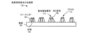
図1Aを参照すると、一例による、表面増強蛍光分光(SEFS)装置100の略側面図が示されている。本明細書に開示されるSEFS装置100の範囲から外れることなく、図1Aに示されているSEFS装置100は、他のコンポーネントを含む場合があり、また、本明細書に記載されるコンポーネントの一部は、取り除かれ、及び/又は、変更が加えられる場合があるものと理解すべきである。また、図1Aに示したコンポーネントは、実寸どおりに描かれていない場合があり、したがって、それらのコンポーネントは互いに、図示したものとは異なる相対的サイズを有する場合があるものと理解すべきである。
Referring to FIG. 1A, a schematic side view of a surface enhanced fluorescence spectroscopy (SEFS)
SEFS装置100は、基板102と、基板102の表面の上に延びる複数のナノ・フィンガー104とを含む場合がある。図1Aにおいて、ナノ・フィンガー104は、以下で詳しく説明されるように、ナノ・フィンガー104の互いに対する部分的傾倒の後の状態を示している場合がある。
The
SEFS装置100は、ナノ・フィンガー104の先端108上に配置された複数の表面増強分光(SES)要素106をさらに含む場合がある。以下で説明されるように、SES要素106は、ナノ・フィンガー104が部分的に傾倒されるよりも前に、ナノ・フィンガー104の先端108上に配置される場合がある。その結果、ナノ・フィンガー108が互いに向けて部分的に傾倒するにしたがって、先端108上に配置されたSES要素106もまた、相対的に近接した状態(例えば、ナノメートル未満の距離だけ離れた状態)となり、及び/又は、互いに接触した状態になる場合がある。互いに比較的近接した状態にある、及び/又は、接触した状態にあるSES要素106は、SES要素106の個々のクラスタ110を成しているものとみなされる場合がある。一例によれば、金と金の結合、及び、ジチオール、ジミアン等のような分子の結合(図示せず)のいずれか一方または両方によって、クラスタ110内のSES要素106を互いに結合させることを可能にするために、クラスタ110内のSES要素106は、そのクラスタ110内の他のSES要素106と十分に近接した状態にされる場合がある。
The
一般に、SES要素106は、SES要素106と接触した状態にある粒子、及び/又はSES要素106と比較的近接した状態にある粒子によって、光の放射(例えば、ラマン散乱、蛍光、発光など)を増強し、ひいては、かかる粒子における表面増強ラマン分光(SERS)、増強されたフォトルミネッセンス、増強された蛍光発光等のような検知処理を向上させる要素である場合がある。SES要素106は、例えば、プラズモニック・ナノ粒子又はナノ構造を含む場合があり、プラズモニック・ナノ粒子又はナノ構造は、金(Au)、銀(Ag)、及び同(Cu)のような、ただしそれらに限定されないプラズモン支持材料である場合がある。
In general, the
SES要素106は、ナノスケールの表面粗さを有する場合があり、かかる表面粗さは一般に、プラズモン支持材料層(複数可)の堆積中に自然に生成されることがある、層(複数可)の表面におけるナノスケール表面形状によって特徴付けられる場合がある。本明細書における定義によれば、プラズモン支持材料は、分光中に、材料上に置かれた検体、又は材料の近くにある検体からの信号の分散、及び信号の生成若しくは放射を可能にする材料である場合がある。
The
一部の例において、SES要素106は、ターゲット分子の吸収を可能にする機能を有する場合がある。例えば、SES要素106の表面は、特定種類の検体をSES要素に取り付け、又は、結合させ、若しくは優先的に吸収させることができるような機能を有する場合がある。特定の例として、SES要素106は、例えば、特定タイプの細胞、組織などに含まれる場合があるターゲット分子に取り付けることができる機能を有する場合がある。
In some examples, the
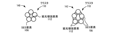
次に、図1B及び図1Cを参照すると、種々の例によるSES要素106のクラスタ110の種々の例示的構成を示す、例えば図1AのSEFS装置100の一部を上から見たような簡略図が示されており、この構成では、SES要素106の間に蛍光増強要素112が捕捉される場合がある。一般に、図1B及び図1Cに示されている図は、蛍光増強要素112の導入の後、ナノ・フィンガー104が図1Aに示されているように部分的に傾倒された結果として起こり得る、SES要素106(及び、蛍光要素112)の配置の種々の例を示している。したがって、図1B及び図1Cに示した図は、単に例示の目的で提供されるものであり、本開示の例の範囲から外れることなく、任意数の代替構成が形成される場合があるものと理解すべきであり、代替構成は、図示したものとは異なる数のSES要素106、及び/又は蛍光増強要素112を含む場合がある。
Referring now to FIGS. 1B and 1C, a simplified diagram, such as a top view of a portion of the
一般に、蛍光増強要素112は、化学的、及び/又は生物学的ターゲット分子の検出を増強することができる要素である場合がある。例えば、蛍光増強要素112は、蛍光要素112が捕捉されるSES要素106のクラスタ110に比較的近接した状態にあるターゲット分子の蛍光を増強する要素である場合がある。他の例として、蛍光増強要素112は、それ自体が蛍光を増強するものではなく、他の粒子又は分子と結合したときに蛍光を増強する要素である場合がある。個別に蛍光を増強させることができ、及び/又は、他の粒子若しくは分子との結合によって蛍光を増強させることができる蛍光増強要素112の例は、本明細書において説明される。
In general, the
蛍光増強要素112は、蛍光染料、蛍光プローブ、ターゲット分子と結合された蛍光分子、非蛍光イオン指示薬、金属イオンと結合された非蛍光イオン指示薬等のうちの何れであってもよい。いずれの場合も、蛍光要素112は、ナノ・フィンガー104の部分的傾倒よりも前にSES要素106の間に導入される場合があり、それによって、ナノ・フィンガー104が部分的に傾倒した後、SES要素106の間に蛍光増強要素112を捕捉することが可能となる。さらに、蛍光増強要素112が要素の結合を含む例では、要素の1つが、ナノ・フィンガー104の部分的傾倒よりも前に導入され、要素の別の1つが、ナノ・フィンガー104の部分的傾倒の後に導入される場合がある。これらの例において、蛍光増強要素112は、要素が互いに結合されるまで、蛍光を増強しない場合がある。
The
まず、図1Bを参照すると、最初の図120は、クラスタ110の3つのSES要素106の間に、1つの蛍光増強要素112が捕捉される場合がある例を示している。2番目の図130は、クラスタ110の3つのSES要素106の各々の間に、3つの蛍光増強要素112が捕捉される場合がある例を示している。図1Cに示されてるように、最初の図140は、クラスタ110の5つのSES要素106の間に、1つの蛍光増強要素112が捕捉される場合がある例を示している。また、2番目の図142は、クラスタ110の5つのSES要素106の間に、5つの蛍光増強要素112が捕捉される場合がある例を示している。図1B及び図1Cには示されていないが、蛍光増強要素112は、クラスタ110の全部ではなく一部のSES要素106の間に捕捉される場合がある。追加及び/又は代替として、クラスタ110の一部のSES要素106は、金と金の結合、及び/又は、分子の結合(図示せず)によって、互いに結合される場合がある。
Referring first to FIG. 1B, the initial diagram 120 illustrates an example where one
次に図2を参照すると、一例による、SEFS装置100を形成するための方法200を示すフロー図が示されている。図2に示されている方法200は、方法200の範囲から外れることなく、他の処理を含む場合があり、また、記載された処理の一部が取り除かれ、及び/又は、変更が加えられる場合があるものと理解すべきである。方法200に関して実施される場合がある種々の他の処理の例は、以下に提供される。
Referring now to FIG. 2, a flow diagram illustrating a
ブロック202では、複数のSES要素106が、複数のナノ・フィンガー104の先端108上に堆積される場合があり、その場合、複数のナノ・フィンガー104は、基板102から延びていて、かつ互いに十分に近接した状態で配置される場合があり、それによって、ナノ・フィンガー104が部分的に傾倒されたときに、一群の隣り合うナノ・フィンガー104の先端108を互いに十分に近接した状態にすることが可能となり、先端108上のSES要素106は、蛍光増強要素112を捕捉することが可能となる。すなわち、一群のナノ・フィンガー104における複数のナノ・フィンガー104は、互いに十分に近接した状態で配置される場合があり、それによって、一群のナノ・フィンガーにおけるナノ・フィンガー104が部分的に傾倒されたときに、それらのナノ・フィンガー104の先端108上のSES要素106は、SES要素106の間に蛍光増強要素112を捕捉することが可能となる。例として、一群のナノ・フィンガー104は、各群のナノ・フィンガー104上のSES要素106が約1ナノメートル未満の間隔で配置されることになるように、十分に近接した状態で配置される場合がある。
At block 202, a plurality of
ブロック204では、蛍光増強要素112が、SES要素106の間に導入される場合がある。一例によれば、蛍光増強要素112は、溶液に含まれる場合があり、溶液は、基板102、ナノ・フィンガー104、及びSES要素106の上に設けられる場合がある。他の例として、基板102、ナノ・フィンガー104、及びSES要素106は、例えば、蛍光増強要素112を含む溶液の中に提供され、例えば浸される場合がある。
At block 204,
ブロック206では、一群の隣り合うナノ・フィンガー104におけるナノ・フィンガー104が、互いに向けて部分的に傾倒される場合があり、それによって、一群のナノ・フィンガー104の先端108上の複数のSES要素106は、互いに十分に近接した状態(例えば、約1ナノメートル未満)となり、複数のSES要素106の間に、蛍光増強要素112のうちの1つの蛍光増強要素112を捕捉する。本明細書に記載されるように、ナノ・フィンガー104は、各群におけるナノ・フィンガー104が互いに向けて部分的に傾倒されるような形で(したがって、他の群のナノ・フィンガー104に向けて部分的に傾倒されないような形で)、基板102上に作成される場合がある。同様に本明細書に記載されるように、ナノ・フィンガー104は、ナノ・フィンガー104間に対する流体の導入及び除去によって、互いに向けて部分的に傾倒される場合がある。
At
図3A及び図3Bを参照すると、SEFS装置100の等角図、及び、図3AのラインA−Aに沿って切断して見たときのSEFS装置100の断面図が、それぞれ示されている。図3A、及び図3Bは、図1Aとともに、一例による、SEFS装置100の種々の製造工程を示している。したがって、この点に関し、図1A、図3A及び図3Bの図は、方法200において実施される処理を、それらの処理に対する多少の変更とともに示している場合がある。本明細書に開示されるSEFS装置100の範囲から外れることなく、図3A及び図3Bに示されたSEFS装置100は、他のコンポーネントを含む場合があり、また、本明細書に記載されるコンポーネントの一部は、取り除かれ、及び/又は変更が加えれる場合があるものと理解すべきである。また、図3A及び図3Bに示されたコンポーネントは、実寸どおりに描かれておらず、したがって、それらのコンポーネントは、各々に関して、図示したものとは異なる相対的サイズを有する場合があるものと理解すべきである。
Referring to FIGS. 3A and 3B, an isometric view of the
図3A及び図3Bに示されているSEFS装置100は、図1Aに示されているものと同じ機能を有する場合がある。図3Aに示されているSEFS装置100は、図3Aに示されているSEFS装置100のナノ・フィンガー104は事前傾倒状態にある場合がある点で、図1Aに示されているSEFS装置100とは異なる場合がある。この点に関し、図3Aは、図2Aのブロック202の後のSEFS装置100を示している場合があり、図2Aのブロック202では、ナノ・フィンガー104の先端108上にSES要素106が堆積される場合がある。
The
基板102は、ケイ素、窒化ケイ素、ガラス、石英、サファイア、ダイヤモンド、ダイヤモンド・ライク・カーボン、プラスチック、ポリマー、ケイ素酸化物(SiO2)、アルミニウム酸化物(Al2O3)、アルミニウム、それらの材料の組み合わせ等のような材料から形成される場合がある。基板102は、シート、ウェーハ、薄膜、及びウェブからなる一群の中から選択された形態を有する場合がある。例えば、基板102は、ウェブの形態を有する場合があり、基板102は、ロール・ツー・ロール製造プロセスにおける材料のロールのようなフィードストックとして使用される場合がある。別の例として、基板102は、ポリイミド、ポリエチレン、ポリプロピレン、又は何らかの他の適当な高分子プラスチックのようなプラスチック材料からなる可撓性ポリマーフィルムの形態を有する場合がある。したがって、一例によれば、基板102は、半導体ウェーハのような剛性のものである場合もあれば、ウェブのように可撓性のものである場合もがある。
The
ナノ・フィンガー104は、ナノメートル範囲の寸法を有する場合があり、例えば、約500nm未満の寸法を有する場合があり、比較的柔軟な材料から形成される場合があり、及び/又は、比較的高いアスペクト比を有する場合があり、その結果、例えば、ナノ・フィンガー104を横方向に曲げること、すなわち、傾倒させることが可能となり、例えば、ナノ・フィンガー104の先端を図1Aに示されているように互いに対して相対的に近接した状態にすることが可能となる。例えば、ナノ・フィンガー104が部分的に傾倒されたとき、互いに近接した状態となるナノ・フィンガー104の先端は、先端間に、1ナノメートル未満のサイズのギャップを有する場合がある。ナノ・フィンガー104のための適当な材料の例には、UV硬化可能又は熱硬化可能なインプリンティング・レジスト、ポリアクリル酸アルキル、ポリシロキサン、ポリジメチルシロキサン(PDMS)エラストマー、ポリイミド、ポリエチレン、ポリプロピレン、ポリウレタン、フッ素ポリマーなど、又はそれらの任意の組み合わせのようなポリマー材料、金、銀、アルミニウム等のような金属材料、半導体材料等、及び、それらの組み合わせが含まれ得る。
Nano-
ナノ・フィンガー104は、任意の適当な取り付け手段によって、基板102の表面に取り付けることができる。例えば、ナノ・フィンガー104は、種々の適当なナノ構造成長技術のうちの任意の実施形態を使用して、基板102の表面上に直接成長される場合がある。別の例として、ナノ・フィンガー104は、基板102と一体的に形成される場合がある。この例では、例えば、基板102を製造する元になる材料の一部をエッチングし、又は他の加工を施すことにより、ナノ・フィンガー104が形成される場合がある。さらに別の例では、独立した材料の層を基板102の表面に接着し、独立した材料の層をエッチングし、又は他の加工を施すことにより、ナノ・フィンガー104が形成される場合がある。種々の例において、ナノ・フィンガー104は、ナノ・インプリンティング又はエンボス・プロセスによって製造される場合があり、その場合、ポリマー・マトリックスに対する多工程インプリンティングプロセスにおいて、比較的硬い複数の柱からなるテンプレートを使用して、ナノ・フィンガー104が形成される場合がある。こうした例では、テンプレートは、ナノ・フィンガー104を所定の構成で配置するための所望のパターンを使用して、フォトリソグラフィ又は他の進んだリソグラフィ技術により形成される場合がある。より具体的には、例えば、所望のパターンは、電子ビームリソグラフィ、集束イオンビーム(FIB)リソグラフィ、球の自己組織化などのうちの任意のものによってモールド上にデザインされる場合がある。さらに、パターンは、他の基板上に転写される場合があり、例えば、ケイ素、ガラス、又はポリマー基板(ポリジメチルシロキサン(PDMS)、ポリイミド、ポリカーボネートなど)に転写される場合がある。エッチングのような種々の他のプロセス、並びに、電気機械システム(MEMS)及びナノ電気機械システム(NEMS)の製造において使用される種々の技術もまた、ナノ・フィンガー104を製造するために使用される場合がある。
Nano-
ナノ・フィンガー104は、実質的にランダムな分布で配置される場合もあれば、又は、ナノ・フィンガー104は、所定の構成を成すように配置される場合もある。いずれに関しても、一例によれば、ナノ・フィンガー104は互いに対して、ナノ・フィンガー104が部分的に傾倒した状態になったときに、少なくとも2つの隣り合うナノ・フィンガー104を互いに近接した状態にすることができるように配置される場合がある。特定の例として、隣り合うナノ・フィンガー104は、約100ナノメートル未満の距離だけ互いに離して配置される場合がある。特定の例によれば、ナノ・フィンガー104は、ナノ・フィンガー104のうちの隣り合うものが優先的に部分的に傾倒し、所定の形状、例えば、三角形、正方形、五角形などを形成するように、基板102上にパターニングされる場合がある。
The
次に、図3Bを参照すると、一例による、図3AのラインA−Aに沿って切断して見たときの装置100の断面図が示されている。図面に示されているように、ナノ・フィンガー104の先端108はそれぞれ、その上に配置された個々のSES要素106を含む場合がある。SES要素106は、以下で説明されるように金属ナノ粒子を含む場合があり、例えば、金属材料の物理蒸着(PVD:Physical Vapor Deposition)、化学蒸着(CVD:Chemical Vapor Deposition)、スパッタリング等、又は、事前合成されたナノ粒子の自己組織化のうちの1つによって、ナノ・フィンガー104の先端108上に堆積される場合がある。
Referring now to FIG. 3B, a cross-sectional view of the
図3A及び図3Bにおいて、ナノ・フィンガー104はそれぞれ、垂直に延び、互いに同じ高さを有しているように描かれているが、ナノ・フィンガー104の一部は、互いに種々の角度及び高さで延びている場合もある。ナノ・フィンガー104間における角度及び/又は高さの違いは、例えば、ナノ・フィンガー104の製造の際、及び、ナノ・フィンガー104上へのSES要素106の堆積の際における製造ばらつき又は成長ばらつき等から生じる違いに起因する場合がある。
3A and 3B, the
図3A及び図3Bに示されているように、ナノ・フィンガー104は、第1の位置にあり、この位置において、先端108は、互いに対して実質的に間隔を空けた構成を成し、例えば、先端108の間にギャップ114を有している。先端108の間のギャップ114は、蛍光増強要素112を含む液体又は溶液のような液体をギャップ114内に配置することが可能となるように、十分に大きなサイズのものである場合がある。また、ギャップ114は、ギャップ114に付与された液体が蒸発したときに、例えばナノ・フィンガー104に印加される毛管力又は微小毛管力によって、少なくとも一部のナノ・フィンガー104の先端108を互いに引き寄せることができるように、十分に小さいサイズのものである場合がある。この点に関し、図3Bは、図2のブロック204の後のSEFS装置100を示している場合があり、図2のブロック204では、SES要素106の間に蛍光要素112が導入される場合がある。さらに、液体又は溶液は、各クラスタ110におけるSES要素106を互いに結合させる結合分子をさらに含む場合がある。
As shown in FIGS. 3A and 3B, the
蛍光増強要素112を含む液体又は溶液の少なくとも部分的蒸発の後、ナノ・フィンガー104、SES要素106、及び蛍光増強要素112は、図1Aに示されるような構成を有する場合がある。すなわち、蛍光増強要素112は、SES要素106の各クラスタ110のSES要素の間に捕捉される場合がある。この点に関し、図3Cは、図2のブロック206の後のSEFS装置100を示している場合があり、図2のブロック206では、隣り合うナノ・フィンガーの各群におけるナノ・フィンガー104が、互いに向けて部分的に傾倒される場合があり、それによって、各群のナノ・フィンガーの先端上の複数のSES要素は、互いに十分に近接した状態となり、複数のSES要素間に、蛍光増強要素を捕捉する。
After at least partial evaporation of the liquid or solution containing the
ナノ・フィンガー104は、実質的に円筒形の断面を有しているように描かれている。しかしながら、ナノ・フィンガー104は、他の形状の断面を有する場合もあり、例えば、矩形、正方形、三角形等のような断面を有する場合もあると理解すべきである。例として、ナノ・フィンガー104は、円錐構成を有する場合があり、その場合、基部は基板102に取り付けられ、先端は基板102から遠くに延びる。追加又は代替として、ナノ・フィンガー104は、ナノ・フィンガー104を実質的に特定の方向に傾けて傾倒させるための切り込み、隆起等のような特徴を有するように形成される場合がある。したがって、例えば、2以上の隣り合うナノ・フィンガー104は、ナノ・フィンガー104が互いに向けて傾倒する可能性を増加させるための特徴を含む場合がある。
特定の例によれば、2以上の隣り合うナノ・フィンガー104の群は、互いに向けて傾倒するような特徴を有する場合があり、又は互いに向けて傾倒するように製造される場合があり、それによって、ナノ・フィンガー104が部分的に傾倒されたときに、2以上の隣り合うナノ・フィンガー104の先端が互いに相対的に近接した状態となるように構成される場合がある。他の例において、ナノ・フィンガー104は、ナノ・フィンガー104の群が、群の外にあるナノ・フィンガー104に比べて相対的に近接した状態となるように、基板102上に配置される場合がある。この点に関し、ナノ・フィンガー104上に流体が導入され、その流体が蒸発したとき、各群のナノ・フィンガー104は、それらのナノ・フィンガーに印加される比較的大きな微細毛管力に起因して、互いに向けて傾倒される場合がある。ナノ・フィンガー104を部分的に傾倒させることが可能な種々の態様については、以下で詳細に説明される。
According to certain examples, a group of two or more
一例によれば、蛍光増強要素112は、蛍光染料である場合がある。この例では、溶液が蛍光染料を含んでいて、溶液は、図2のブロック204において、SES要素106の間に導入される場合がある。蛍光染料の例には、限定はしないが、モレキュラー・プローブス社から入手できるアレクサフルオル488染料、アレクサフルオル500染料、アレクサフルオル514染料、アレクサフルオル532染料、アレクサフルオル546染料、アレクサフルオル555染料、アレクサフルオル568染料、アレクサフルオル594染料、アレクサフルオル610染料、アレクサフルオル633染料、アレクサフルオル635染料、アレクサフルオル647染料、アレクサフルオル660染料、アレクサフルオル680染料、アレクサフルオル700染料、アレクサフルオル750染料、アレクサフルオル350染料、アレクサフルオル405染料、アレクサフルオル430染料のようなローダミン系蛍光染料;BODIPY 493/503、BODIPY R6G、BODIPY TMR、BODIPY 558/568、BODIPY 564/570、BODIPY 576/589、BODIPY 581/591、BODIPY TR、BODIPY 630/650、BODIPY 650/655のようなBODIPYフルオロフォア系蛍光染料;オレゴングリーン448カルボン酸、オレゴングリーン514カルボン酸のようなフルオレセイン系蛍光染料;及び他のクマリン又はピレン系蛍光染料が含まれ得る。この例では、溶液は、ブロック206において蒸発される場合があり、それによって、一部のSES要素106の間に捕捉された蛍光染料が残される。
According to one example, the
別の例によれば、蛍光増強要素112は、ターゲット分子と結合するように構成された蛍光プローブ分子である場合がある。蛍光プローブ分子は、特定の色変化をもたらし、又は、異なる蛍光色を放射する任意の分子を表す場合があり、関連ターゲット分子を有する場合もあれば、有しない場合もある。蛍光プローブ分子は、金属イオンの場合のクラウンエーテル等のような、特定の化学的又は生物学的物質と選択的に結合することが可能な受容体を有する場合がある。ターゲット分子とは、関心対象である任意の分子を指す場合があり、ターゲット分子は、共通溶媒に溶解可能である場合がある。例えば、ターゲット分子には、メラミン、殺虫剤、ラクトパミンなどが含まれ得る。共通溶媒には、メタノール、エタノール、イソプロパノール、ヘキサフルオロ・イソプロパノール、トルエン、クロロホルム、テトラヒドロフラン、アセトン、アセトニトリル、キシレン、酢酸エチル、ヘキサン誘導体、ジクロロメタンなどが含まれ得る。例えば、蛍光プローブ分子は、何も蛍光を有しない場合があるが、蛍光プローブ分子がターゲット分子と結合したときに、比較的強い蛍光を示す場合がある。
According to another example, the
一例として、ターゲット分子404は、ナノ・フィンガー104の部分的傾倒の後に続いて導入される場合がある。この例は、図4Aに示されている。図4Aは、SES要素106の各クラスタ110において、蛍光プローブ分子402がSES要素106の間に捕捉される場合がある、一例によるSEFS装置100の略側面図を示している。図4Aでは、SES要素106の間に蛍光プローブ分子404が捕捉された後に続いて、ターゲット分子404を含む溶液が、蛍光プローブ分子402との結合のために導入される場合がある。この例では、ターゲット分子404は、例えば、蛍光プローブ分子402と結合する場合がある。なぜなら、蛍光プローブ分子402が、ターゲット分子と選択的に結合する受容体を含む場合があるからである。
As an example, the
別の例として、蛍光プローブ分子402とターゲット分子404は、ナノ・フィンガー404の部分的傾倒よりも前に、錯体410として結合される場合がある。この例は、図4Bに示されている。図4Bは、SES要素106の各クラスタ110のSES要素106の間に、蛍光プローブ分子とターゲット分子404の錯体410を含む溶液が導入される場合がある、SEFS装置100の略側面図を示している。この例では、ナノ・フィンガー104の部分的傾倒の後に続いて、例えば図2のブロック206において、SEF要素106の間に結合体410が捕捉される場合がある。
As another example,
さらに別の例によれば、蛍光増強要素112は、所定の金属イオン504と選択に結合する非蛍光イオン指示薬502から形成された錯体510である場合がある。この例では、錯体510は、比較的強い蛍光を示す場合がある。金属イオン504と結合し、錯体510を形成する非蛍光イオン指示薬502の化学的構造の例は、図5Aに示されている。
According to yet another example, the
一例として、金属イオン504は、ナノ・フィンガー104の部分的傾倒の後に続いて導入される場合がある。この例は、図5Bに示されている。図5Bは、SES要素106の各クラスタ110においてSES要素106の間に非蛍光イオン指示薬502が捕捉される場合がある、一例によるSEFS装置100の略側面図を示している。図5Bでは、SES要素106の間に非蛍光イオン指示薬502が捕捉された後に続いて、金属イオン504を含む溶液が、非蛍光イオン指示薬502との結合のために導入される場合がある。
As an example,
別の例として、非蛍光イオン指示薬502と金属イオン504は、ナノ・フィンガー104の部分的傾倒よりも前に、錯体510として結合される場合がある。この例は、図5Cに示されている。図5Cは、SES要素106の各クラスタのSES要素106の間に非蛍光イオン指示薬502と金属イオン504の錯体510を含む溶液が導入される場合がある、SEFS装置100の略側面図を示している。この例では、ナノ・フィンガー104の部分的傾倒の後に続いて、例えば、図2のブロック206において、SES要素106の間に錯体510が捕捉される場合がある。
As another example,
さらに別の例によれば、例えば図2のブロック204のような蛍光増強要素112の導入よりも前に、図6に示されているように、SES要素106上に金属酸化物層602がそれぞれ形成される場合がある。この点に関し、金属酸化物層602は、SES要素106を保護するために、SES要素106上に形成される場合がある。金属酸化物層602は、例えば、酸化ケイ素(SiO2)、酸化チタン(TiO2)、酸化亜鉛(ZnO)、酸化アルミニウム、酸化ガリウム、酸化インジウム、酸化ジルコニウム、酸化ハフニウム、酸化タンタル、及びそれらの混合物を含む場合がある。金属酸化物層602は、原子層堆積(ALD:Atomic Layer Deposition)、電子ビームスパッタリング等のような多数の金属酸化物堆積技術のうちの何れによって形成されてもよい。さらに、一例によれば、金属酸化物層602は、約1nmから約200nmまで変化する場合がある厚みを有するように形成される場合がある。さらに別の例として、金属酸化物層の厚みは、約2nmから約50nmまでである場合がある。
According to yet another example, prior to the introduction of the
図6は、さらに、金属酸化物層602の形成の際に、ナノ・フィンガー104の間において基板102上に形成される場合がある残余金属酸化物層604も示している。図6には、金属酸化物層602により覆われたSES要素106のうちの1つの拡大断面図も示されている。拡大断面図に示されているように、金属酸化物層602は、SES要素106の側面及び上部を覆う場合がある。この点に関し、ナノ・フィンガー104が例えば図1Aに示されているように部分的に傾倒された場合、金属酸化物層602は、ナノ・フィンガー104のうちの隣り合うものの上にあるSES要素106の間に配置される場合がある。したがって、SES要素112の各クラスタ110において蛍光増強要素112が捕捉されたとき、蛍光増強要素112は、SES要素106と接触するだけでなく、金属酸化物層602とも接触する場合がある。
FIG. 6 also shows a residual metal oxide layer 604 that may be formed on the
金属酸化物層602は、上で説明した蛍光増強要素112のうちの何れかを捕捉するためのナノ・フィンガー104の部分的傾倒よりも前に、SES要素106上に形成される場合がある。したがって、例えば、蛍光増強要素112が蛍光染料である場合、金属酸化物層602は、蛍光増強要素112の導入よりも前に、SES要素106上に形成される場合がある。
The
別の例として、例えば図4Aを参照して上で説明したように、蛍光増強要素112が、ターゲット分子404と結合するように構成された蛍光プローブ分子402である場合、金属酸化物層602は、蛍光増強要素112の導入よりも前に、SES要素106上に形成される場合がある。さらに別の例として、例えば図4Bを参照して上で説明したように、蛍光増強要素112が、蛍光プローブ分子402とターゲット分子404の錯体である場合、金属酸化物層602は、蛍光増強要素112の導入よりも前に、SES要素106上に形成される場合がある。
As another example, if the
さらに別の例として、例えば図5を参照して上で説明したように、蛍光増強要素112が、所定の金属イオン504と結合するように構成された非蛍光イオン指示薬502である場合、金属酸化物層602は、蛍光増強要素112の導入よりも前に、SES要素106上に形成される場合がある。さらに別の例として、図5Cを参照して上で説明したように、蛍光増強要素112が、非蛍光イオン指示薬502と金属イオン504の錯体510である場合、金属酸化物層602は、蛍光増強要素112の導入よりも前に、SES要素106上に形成される場合がある。
As yet another example, when the
本開示の代表的な種々の例が、この開示全体を通じて具体的に説明されているが、それらは、広範囲の応用形態にわたる有用性を有する場合があり、上記説明に制限の意図はなく、上記説明を制限として解釈すべきではなく、上記説明は、開示の種々の態様の例示的説明として提供されたものである。 While various representative examples of this disclosure have been specifically described throughout this disclosure, they may have utility across a wide range of applications and are not intended to be limiting in the above description. The description should not be construed as limiting, but the above description is provided as exemplary illustrations of various aspects of the disclosure.
本明細書に記載され例示されているものは、ある程度の変形を伴う例である。本明細書において使用される用語、説明、及び図は、例として説明されたものであり、制限を意味するものではない。記載事項の思想及び範囲内において、多数の変形が可能であり、かかる思想及び範囲は、下記の特許請求の範囲、及びそれらの均等によって定義されることが意図されており、特許請求の範囲において、全ての語は、特に断りがない限り、その最も広い妥当な意味で使用されている。 What is described and illustrated herein is an example with some variation. The terms, descriptions, and figures used herein are set forth by way of illustration and are not meant as limitations. Many modifications may be made within the spirit and scope of the description, and the spirit and scope are intended to be defined by the following claims and their equivalents. All terms are used in their broadest reasonable sense unless otherwise noted.
Claims (15)
複数のナノ・フィンガーの各々の先端に複数の表面増強分光(SES)要素を堆積させるステップであって、前記ナノ・フィンガーは互いに十分に近接して配置され、それによって、前記ナノ・フィンガーが部分的に傾倒されたときに、一群の隣り合うナノ・フィンガーの先端を互いに十分に近接した状態にすることが可能となり、前記先端上のSES要素が蛍光増強要素を捕捉することが可能となることを含むステップと、
前記複数のSES要素の間に前記蛍光増強要素を導入するステップと、
前記一群の隣り合うナノ・フィンガーにおけるナノ・フィンガーを互いに向けて部分的に傾倒させ、それによって、前記一群のナノ・フィンガーの先端上の複数のSES要素を互いに十分に近接した状態にし、前記蛍光増強要素のうちの1つの蛍光増強要素を前記複数のSES要素の間に捕捉するステップと
を含む方法。 A method of forming a surface enhanced fluorescence spectroscopy (SEFS) device comprising:
Depositing a plurality of surface enhanced spectroscopic (SES) elements at the tips of each of the plurality of nanofingers, wherein the nanofingers are positioned sufficiently close to each other so that the nanofingers are partially The tip of a group of adjacent nano-fingers can be in close proximity to each other when tilted, and the SES element on the tip can capture the fluorescence enhancing element Including steps,
Introducing the fluorescence enhancing element between the plurality of SES elements;
The nano fingers in the group of adjacent nano fingers are partially tilted towards each other, thereby bringing a plurality of SES elements on the tips of the group of nano fingers in close proximity to each other, and the fluorescence Capturing a fluorescence enhancement element of one of the enhancement elements between the plurality of SES elements.
前記方法は、
前記蛍光増強要素、及び前記複数のSES要素の上に前記ターゲット分子を含む溶液を導入するステップであって、前記ターゲット分子が、前記蛍光プローブ分子と結合するように構成されることを含むステップ
をさらに含む、請求項1に記載の方法。 The fluorescence enhancing element is a fluorescent probe molecule configured to bind to a target molecule;
The method
Introducing the solution containing the target molecule onto the fluorescence enhancing element and the plurality of SES elements, the target molecule being configured to bind to the fluorescent probe molecule. The method of claim 1, further comprising:
前記方法は、
前記蛍光プローブ分子及び前記ターゲット分子を溶液中で結合させるステップであって、前記蛍光プローブ分子が、前記溶液中で前記ターゲット分子と結合するように構成されることを含むステップ
をさらに含み、
前記複数のSES要素の上に前記蛍光増強要素を導入するステップは、結合された前記蛍光プローブ分子及び前記ターゲット分子を前記複数のSES要素の上に導入することをさらに含む、請求項1に記載の方法。 The fluorescence enhancing element is a fluorescent probe molecule configured to bind to a target molecule;
The method
Further comprising the step of binding the fluorescent probe molecule and the target molecule in solution, wherein the fluorescent probe molecule is configured to bind to the target molecule in the solution;
The method of claim 1, wherein introducing the fluorescence enhancing element on the plurality of SES elements further comprises introducing the bound fluorescent probe molecule and the target molecule onto the plurality of SES elements. the method of.
前記方法は、
前記非蛍光イオン指示薬及び前記所定の金属イオンを結合させるステップ
をさらに含み、
前記複数のSES要素の上に前記蛍光増強要素を導入するステップは、前記非蛍光イオン指示薬、又は、前記非蛍光イオン指示薬及び前記所定の金属イオンの結合体を、前記複数のSES要素の上に導入することをさらに含む、請求項1に記載の方法。 The fluorescence enhancing element comprises a complex formed from a non-fluorescent ion indicator that is selectively bound to a predetermined metal ion;
The method
Binding the non-fluorescent ion indicator and the predetermined metal ion;
The step of introducing the fluorescence enhancing element on the plurality of SES elements includes the non-fluorescent ion indicator or a combination of the non-fluorescent ion indicator and the predetermined metal ion on the plurality of SES elements. The method of claim 1, further comprising introducing.
をさらに含み、
前記蛍光増強要素を導入するステップは、前記複数のSES要素上の前記金属酸化物層の上に、前記蛍光増強要素を導入することをさらに含む、請求項1に記載の方法。 Forming each layer of metal oxide on the plurality of SES elements prior to introducing the fluorescence enhancing element;
The method of claim 1, wherein introducing the fluorescence enhancing element further comprises introducing the fluorescence enhancing element over the metal oxide layer on the plurality of SES elements.
前記方法は、
前記蛍光要素、及び前記金属酸化物層の上に、前記ターゲット分子を含む溶液を導入するステップであって、前記ターゲット分子が、前記蛍光プローブ分子と結合するように構成されることを含むステップ
をさらに含む、請求項6に記載の方法。 The fluorescence enhancing element is a fluorescent probe molecule configured to bind to a target molecule;
The method
Introducing a solution containing the target molecule on the fluorescent element and the metal oxide layer, the target molecule comprising: being configured to bind to the fluorescent probe molecule The method of claim 6 further comprising:
前記方法は、
前記蛍光プローブ分子及び前記ターゲット分子を溶液中で結合させるステップであって、前記蛍光プローブ分子が、前記溶液中の前記ターゲット分子と結合するように構成されることを含むステップ
をさらに含み、
前記金属酸化物層の上に前記蛍光増強要素を導入するステップは、結合された前記蛍光プローブ分子及び前記ターゲット分子を前記金属酸化物層の上に導入することをさらに含む、請求項6に記載の方法。 The fluorescence enhancing element is a fluorescent probe molecule configured to bind to a target molecule;
The method
Further comprising the step of binding the fluorescent probe molecule and the target molecule in solution, wherein the fluorescent probe molecule is configured to bind to the target molecule in the solution;
The step of introducing the fluorescence enhancing element on the metal oxide layer further comprises introducing the bound fluorescent probe molecule and the target molecule on the metal oxide layer. the method of.
前記方法は、
前記非蛍光イオン指示薬及び前記所定の金属イオンを結合させるステップ
をさらに含み、
前記金属酸化物層の上に前記蛍光増強要素を導入するステップは、前記非蛍光イオン指示薬、又は、前記非蛍光イオン指示薬及び前記所定の金属イオンの結合体を、前記金属酸化物層の上に導入することをさらに含む、請求項6に記載の方法。 The fluorescence enhancing element comprises a complex formed from a non-fluorescent ion indicator that is selectively bound to a predetermined metal ion;
The method
Binding the non-fluorescent ion indicator and the predetermined metal ion;
The step of introducing the fluorescence enhancing element onto the metal oxide layer includes the step of bringing the non-fluorescent ion indicator or the combination of the non-fluorescent ion indicator and the predetermined metal ion onto the metal oxide layer. The method of claim 6, further comprising introducing.
前記SES要素上に形成された金属酸化物層と、
前記SES要素のクラスタにおいて前記SES要素の間に捕捉された蛍光増強要素と
を含む、表面増強蛍光分光(SEFS)装置。 A cluster of SES elements comprising at least two surface enhanced spectroscopy (SES) elements in at least one of a state in contact with each other and a state in proximity to each other;
A metal oxide layer formed on the SES element;
A surface-enhanced fluorescence spectroscopy (SEFS) apparatus comprising: a fluorescence enhancing element captured between the SES elements in the cluster of SES elements.
Applications Claiming Priority (1)
| Application Number | Priority Date | Filing Date | Title |
|---|---|---|---|
| PCT/US2013/023863 WO2014120156A1 (en) | 2013-01-30 | 2013-01-30 | Surface enhanced fluorescence spectroscopy apparatus |
Publications (1)
| Publication Number | Publication Date |
|---|---|
| JP2016505157A true JP2016505157A (en) | 2016-02-18 |
Family
ID=51262723
Family Applications (1)
| Application Number | Title | Priority Date | Filing Date |
|---|---|---|---|
| JP2015555973A Pending JP2016505157A (en) | 2013-01-30 | 2013-01-30 | Surface-enhanced fluorescence spectrometer |
Country Status (5)
| Country | Link |
|---|---|
| US (2) | US9702821B2 (en) |
| EP (1) | EP2951561A4 (en) |
| JP (1) | JP2016505157A (en) |
| CN (1) | CN104969060B (en) |
| WO (1) | WO2014120156A1 (en) |
Cited By (1)
| Publication number | Priority date | Publication date | Assignee | Title |
|---|---|---|---|---|
| JP2021517249A (en) * | 2018-04-06 | 2021-07-15 | ヒューレット−パッカード デベロップメント カンパニー エル.ピー.Hewlett‐Packard Development Company, L.P. | Luminescence enhancement system |
Families Citing this family (7)
| Publication number | Priority date | Publication date | Assignee | Title |
|---|---|---|---|---|
| US10174363B2 (en) | 2015-05-20 | 2019-01-08 | Quantum-Si Incorporated | Methods for nucleic acid sequencing |
| TW201725385A (en) * | 2016-01-05 | 2017-07-16 | 財團法人工業技術研究院 | Raman detecting chip for thin layer chromatography and method for separating and detecting an analyte |
| US11125693B2 (en) | 2017-01-31 | 2021-09-21 | Hewlett-Packard Development Company, L.P. | Surface enhanced infrared absorption stage |
| US11402332B2 (en) | 2017-01-31 | 2022-08-02 | Hewlett-Packard Development Company, L.P. | Surface enhanced luminescence sensor nano finger |
| WO2018143924A1 (en) * | 2017-01-31 | 2018-08-09 | Hewlett-Packard Development Company, L.P. | Nano fingers with asymmetric material composition |
| US11351760B2 (en) | 2017-11-27 | 2022-06-07 | Washington University | Plasmonic patch as a universal fluorescence enhancer |
| US11038011B2 (en) * | 2019-10-29 | 2021-06-15 | Globalfoundries U.S. Inc. | Metal-insulator-metal capacitors including nanofibers |
Citations (6)
| Publication number | Priority date | Publication date | Assignee | Title |
|---|---|---|---|---|
| JP2009544967A (en) * | 2006-07-25 | 2009-12-17 | ヒューレット−パッカード デベロップメント カンパニー エル.ピー. | Controllable surface enhanced Raman spectroscopy |
| US20110166045A1 (en) * | 2009-12-01 | 2011-07-07 | Anuj Dhawan | Wafer scale plasmonics-active metallic nanostructures and methods of fabricating same |
| US20120092660A1 (en) * | 2010-10-15 | 2012-04-19 | Wei Wu | Apparatus for performing sers |
| WO2012054027A1 (en) * | 2010-10-20 | 2012-04-26 | Hewlett-Packard Development Company, L.P. | Chemical-analysis device integrated with metallic-nanofinger device for chemical sensing |
| US20120164745A1 (en) * | 2010-12-27 | 2012-06-28 | Kai-Mei Camilla Fu | Nanofinger device with magnetizable portion |
| WO2012124310A1 (en) * | 2011-03-11 | 2012-09-20 | B.R.A.H.M.S Gmbh | Rare earth metal complex having phenanthroline compound as ligand |
Family Cites Families (20)
| Publication number | Priority date | Publication date | Assignee | Title |
|---|---|---|---|---|
| US7531136B2 (en) | 2001-11-26 | 2009-05-12 | Sony Deutschland Gmbh | Chemical sensor |
| WO2004060044A2 (en) | 2003-01-02 | 2004-07-22 | Bioforce Nanosciences, Inc. | Method and apparatus for molecular analysis in small sample volumes |
| US20050191665A1 (en) * | 2003-12-29 | 2005-09-01 | Xing Su | Composite organic-inorganic nanoclusters |
| US7233711B1 (en) | 2005-05-11 | 2007-06-19 | Hewlett Packard Development Company, L.P. | Autonomous evanescent optical nanosensor |
| US7648834B2 (en) | 2006-01-17 | 2010-01-19 | Moore Wayne E | Plasmon fluorescence augmentation for chemical and biological testing apparatus |
| CN101443459A (en) | 2006-05-16 | 2009-05-27 | 皇家飞利浦电子股份有限公司 | Sample control for correction of sample matrix effects in analytical detection methods |
| US7869030B2 (en) * | 2007-01-03 | 2011-01-11 | Research Foundation Of State University Of New York | Aggregates of plural transition metal nanoparticles and plural cyanine dye molecules |
| WO2008123927A1 (en) | 2007-04-05 | 2008-10-16 | The Board Of Trustees Of The University Of Illinois | Biosensors with porous dielectric surface for fluorescence enhancement and methods of manufacture |
| US20090004670A1 (en) * | 2007-06-29 | 2009-01-01 | Jingwu Zhang | Methods for fabricating surface enhanced fluorescent (sef) nanoparticles and their applications in bioassays |
| WO2009011674A1 (en) | 2007-07-13 | 2009-01-22 | Western Michigan University Research Foundation | Trans-1,2-diphenylethylene derivatives and nanosensors made therefrom |
| WO2009051703A1 (en) | 2007-10-15 | 2009-04-23 | The Charles Stark Draper Laboratory, Inc. | Ion-selective sensors |
| US8258450B1 (en) | 2008-06-26 | 2012-09-04 | University Of South Florida | Physical and chemical integrated flow imaging device |
| CN101446547A (en) | 2008-11-06 | 2009-06-03 | 郑州大学 | Zinc and copper ion fluorescence probe and preparation method and application thereof |
| WO2010129787A2 (en) | 2009-05-08 | 2010-11-11 | The Johns Hopkins University | Single molecule spectroscopy for analysis of cell-free nucleic acid biomarkers |
| EP2561337A4 (en) | 2010-04-20 | 2013-12-25 | Hewlett Packard Development Co | Multi-pillar structure for molecular analysis |
| WO2012030870A1 (en) * | 2010-08-30 | 2012-03-08 | Mks Technology (D/B/A Snowy Range Instruments) | Spectroscopic assays and tagging |
| US8404491B2 (en) | 2010-10-29 | 2013-03-26 | Hewlett-Packard Development Company, L.P. | Luminescent chemical sensor integrated with at least one molecular trap |
| WO2012128773A1 (en) | 2011-03-24 | 2012-09-27 | Hewlett-Packard Development Company, L.P. | Apparatus for use in sensing applications |
| WO2012161683A1 (en) | 2011-05-20 | 2012-11-29 | Hewlett-Packard Development Company L.P. | Surface enhanced raman spectroscopy sensor, system and method of sensing |
| US8848183B2 (en) | 2011-07-22 | 2014-09-30 | Hewlett-Packard Development Company, L.P. | Apparatus having nano-fingers of different physical characteristics |
-
2013
- 2013-01-30 WO PCT/US2013/023863 patent/WO2014120156A1/en active Application Filing
- 2013-01-30 EP EP13873373.8A patent/EP2951561A4/en not_active Withdrawn
- 2013-01-30 CN CN201380071844.9A patent/CN104969060B/en not_active Expired - Fee Related
- 2013-01-30 JP JP2015555973A patent/JP2016505157A/en active Pending
- 2013-01-30 US US14/762,415 patent/US9702821B2/en active Active
-
2017
- 2017-07-10 US US15/646,041 patent/US10393662B2/en not_active Expired - Fee Related
Patent Citations (6)
| Publication number | Priority date | Publication date | Assignee | Title |
|---|---|---|---|---|
| JP2009544967A (en) * | 2006-07-25 | 2009-12-17 | ヒューレット−パッカード デベロップメント カンパニー エル.ピー. | Controllable surface enhanced Raman spectroscopy |
| US20110166045A1 (en) * | 2009-12-01 | 2011-07-07 | Anuj Dhawan | Wafer scale plasmonics-active metallic nanostructures and methods of fabricating same |
| US20120092660A1 (en) * | 2010-10-15 | 2012-04-19 | Wei Wu | Apparatus for performing sers |
| WO2012054027A1 (en) * | 2010-10-20 | 2012-04-26 | Hewlett-Packard Development Company, L.P. | Chemical-analysis device integrated with metallic-nanofinger device for chemical sensing |
| US20120164745A1 (en) * | 2010-12-27 | 2012-06-28 | Kai-Mei Camilla Fu | Nanofinger device with magnetizable portion |
| WO2012124310A1 (en) * | 2011-03-11 | 2012-09-20 | B.R.A.H.M.S Gmbh | Rare earth metal complex having phenanthroline compound as ligand |
Non-Patent Citations (1)
| Title |
|---|
| JPN6016002544; Yamaguchi T , et.al.: '"Characterization of cap-shaped silver particles for surface-enhanced fluorescence effects"' ANALYTICAL BIOCHEMISTRY Vol.364, 20070224, p.171-179 * |
Cited By (2)
| Publication number | Priority date | Publication date | Assignee | Title |
|---|---|---|---|---|
| JP2021517249A (en) * | 2018-04-06 | 2021-07-15 | ヒューレット−パッカード デベロップメント カンパニー エル.ピー.Hewlett‐Packard Development Company, L.P. | Luminescence enhancement system |
| US11280740B2 (en) | 2018-04-06 | 2022-03-22 | Hewlett-Packard Development Company, L.P. | Luminescence-enhancement systems |
Also Published As
| Publication number | Publication date |
|---|---|
| US20150355093A1 (en) | 2015-12-10 |
| WO2014120156A1 (en) | 2014-08-07 |
| CN104969060B (en) | 2017-03-08 |
| US9702821B2 (en) | 2017-07-11 |
| EP2951561A1 (en) | 2015-12-09 |
| CN104969060A (en) | 2015-10-07 |
| US20170315058A1 (en) | 2017-11-02 |
| EP2951561A4 (en) | 2016-12-07 |
| US10393662B2 (en) | 2019-08-27 |
Similar Documents
| Publication | Publication Date | Title |
|---|---|---|
| JP2016505157A (en) | Surface-enhanced fluorescence spectrometer | |
| KR101886619B1 (en) | Surface Enhanced Raman Scattering Substrate, Device for Detecting Molecule and the Fabrication Method thereof | |
| López-Lorente | Recent developments on gold nanostructures for surface enhanced Raman spectroscopy: Particle shape, substrates and analytical applications. A review | |
| JP5823053B2 (en) | Apparatus for use in sensing applications and method for fulfilling sensing applications | |
| US7397558B2 (en) | Ordered array of nanoparticles for efficient nanoenhanced Raman scattering detection and methods of forming the same | |
| TWI485389B (en) | Surface enhanced raman spectroscopy sensor, system and method of sensing | |
| JP5848458B2 (en) | Device for filtering chemical species | |
| US10161874B2 (en) | Polarization dependent surface enhanced Raman scattering system | |
| KR101097205B1 (en) | Fabrication method of substrate for surface enhanced raman scattering | |
| US20060146323A1 (en) | Nanowires for surface-enhanced raman scattering molecular sensors | |
| US20130040862A1 (en) | Multi-pillar structure for molecular analysis | |
| US20140024131A1 (en) | Hybrid nanostructures for molecular analysis | |
| JP2013525785A (en) | Self-aligned luminescence enhancement device for surface enhanced luminescence | |
| US8848183B2 (en) | Apparatus having nano-fingers of different physical characteristics | |
| US9310306B2 (en) | Apparatus for use in sensing applications | |
| KR101844979B1 (en) | Substrate comprising plasmonic multiple nanostructures and preparing method thereof | |
| JP4739859B2 (en) | Fine particle assembly array substrate, method for producing the same, and method for analyzing trace substances using the substrate | |
| JP2016508601A (en) | Apparatus having surface-sensitized spectroscopy elements on the outer surface | |
| Golubewa et al. | Stable and Reusable Lace-like Black Silicon Nanostructures Coated with Nanometer-Thick Gold Films for SERS-Based Sensing | |
| EP3625526B1 (en) | A spectroscopic device including design groups | |
| KR20140000817A (en) | Fabrication method for fluorescence signal amplification substrate and the micro array chip thereby | |
| Chang | Development of novel series and parallel sensing system based on nanostructured surface enhanced Raman scattering substrate for biomedical application |
Legal Events
| Date | Code | Title | Description |
|---|---|---|---|
| A621 | Written request for application examination |
Free format text: JAPANESE INTERMEDIATE CODE: A621 Effective date: 20150729 |
|
| A871 | Explanation of circumstances concerning accelerated examination |
Free format text: JAPANESE INTERMEDIATE CODE: A871 Effective date: 20150729 |
|
| A975 | Report on accelerated examination |
Free format text: JAPANESE INTERMEDIATE CODE: A971005 Effective date: 20160104 |
|
| A131 | Notification of reasons for refusal |
Free format text: JAPANESE INTERMEDIATE CODE: A131 Effective date: 20160126 |
|
| A521 | Written amendment |
Free format text: JAPANESE INTERMEDIATE CODE: A523 Effective date: 20160318 |
|
| A02 | Decision of refusal |
Free format text: JAPANESE INTERMEDIATE CODE: A02 Effective date: 20160517 |