JP2016166896A - Nano-gap transducer with selective surface immobilization site - Google Patents
Nano-gap transducer with selective surface immobilization site Download PDFInfo
- Publication number
- JP2016166896A JP2016166896A JP2016098008A JP2016098008A JP2016166896A JP 2016166896 A JP2016166896 A JP 2016166896A JP 2016098008 A JP2016098008 A JP 2016098008A JP 2016098008 A JP2016098008 A JP 2016098008A JP 2016166896 A JP2016166896 A JP 2016166896A
- Authority
- JP
- Japan
- Prior art keywords
- electrode
- preferentially
- electrodes
- functionalizable
- conductive diamond
- Prior art date
- Legal status (The legal status is an assumption and is not a legal conclusion. Google has not performed a legal analysis and makes no representation as to the accuracy of the status listed.)
- Granted
Links
Images


Abstract
Description
関連出願の相互参照
本願は、2009年12月31日付け米国特許出願第12/655,578号「Nanogap Chemical and Biochemical Sensors」(係属中)、2005年3月4日付け米国特許出願第11/073,160号「Sensor Arrays and Nucleic Acid Sequencing Applications」の利益を主張する一部継続出願である2005年9月13日付け米国特許出願第11/226,696号「Sensor Arrays and Nucleic Acid Sequencing Applications」(係属中)、および2007年12月31日付け米国特許出願第11/967,600号「Electronic Sensing for Nucleic Acid Sequencing」(係属中)と関連しており、それらの開示内容を本願明細書に援用する。
This application is related to US patent application Ser. No. 12 / 655,578 “Nanogap Chemical and Biochemical Sensors”, pending Dec. 31, 2009, U.S. Patent Application No. 11/11, Mar. 4, 2005. No. 073,160 “Sensor Arrays and Nucleic Acid Sequencing Applications” US Patent Application No. 11 / 226,696, “Sensor Arrays and Nucleic Acids Aids,” which is a continuation-in-part application claiming the benefits of “Sensor Arrays and Nucleic Acid Sequencing Applications”. (Pending), and US patent application Ser. No. 11 / 967,600, December 31, 2007, “Electronic Sensing for N” cleic Acid Sequencing "(pending) is associated with, incorporated by reference the disclosures herein.
本発明の実施形態は一般的に、トランスデューサ、ナノギャップ・トランスデューサ、電子的センシング、電気化学、酸化還元サイクル、および生体分子検出に関する。 Embodiments of the present invention generally relate to transducers, nanogap transducers, electronic sensing, electrochemistry, redox cycles, and biomolecule detection.
高い精度および/もしくは堅牢性の提供、分析サンプルの所要量の低減、ならびに/または高いスループットの提供が可能な分析装置は、有益な分析・生物医学ツールである。また、小型で大量生産可能な分子検出プラットフォームを用いれば、以前には不可能であった場所および状況において、多くの人々が手頃な価格の疾患検出を利用可能となる。手頃な価格の分子診断装置が入手できることから、利用可能な健康管理のコストが低下するとともに、その品質が向上する。さらに、携帯用の分子検出装置は、セキュリティおよび危険の検出および改善の分野において利用されており、認識されたセキュリティもしくは偶発的な生物学的または化学的な危険に対して迅速かつ適切に対応可能となる。 Analytical devices that can provide high accuracy and / or robustness, reduce analysis sample requirements, and / or provide high throughput are valuable analytical and biomedical tools. In addition, using a small, mass-produced molecular detection platform, many people have access to affordable disease detection in places and situations that were not possible before. The availability of affordable molecular diagnostic equipment reduces the cost of available health care and improves its quality. In addition, portable molecular detectors are used in the areas of security and hazard detection and improvement, and can respond quickly and appropriately to recognized security or accidental biological or chemical hazards. It becomes.
生体の遺伝情報は、デオキシリボ核酸(deoxyribonucleic acid:DNA)およびリボ核酸(ribonucleic acid:RNA)等の非常に長い核酸分子の形態で含まれている。天然由来のDNA分子およびRNA分子は通常、ヌクレオチドと称する繰り返しの化学的構成単位構成されている。たとえば、ヒトゲノムは、およそ30億個のヌクレオチドのDNA配列と、推定2万〜2万5千個の遺伝子とを含む。 Biological genetic information is included in the form of very long nucleic acid molecules such as deoxyribonucleic acid (DNA) and ribonucleic acid (RNA). Naturally derived DNA and RNA molecules are usually composed of repeated chemical building blocks called nucleotides. For example, the human genome contains a DNA sequence of approximately 3 billion nucleotides and an estimated 20,000-25,000 genes.
これまで、ヒトゲノムの30億個のヌクレオチド配列すべてを決定することにより、癌、嚢胞性線維症、および鎌状赤血球貧血等の多くの疾患の遺伝学的根拠を識別するための基礎を築いてきた。個々人のゲノムまたはその一部の配列を決定することによって、医療を個別にオーダーメイドする機会が与えられる。また、たとえば病原体検出すなわち病原体またはその遺伝的変異体の有無の検出等、研究、環境保護、食品安全、生物兵器防衛、および臨床応用においても、核酸配列情報が必要とされている。 So far, determining all 3 billion nucleotide sequences of the human genome has laid the foundation for identifying the genetic basis of many diseases such as cancer, cystic fibrosis, and sickle cell anemia. . By determining the sequence of an individual's genome or a portion thereof, an opportunity to tailor medical care is provided. Nucleic acid sequence information is also required in research, environmental protection, food safety, biological weapon defense, and clinical applications, such as pathogen detection, ie, the presence or absence of a pathogen or its genetic variant.
超低濃度で生体反応および分子を検出できる能力は、たとえば分子検出・分析、分子診断、疾患検出、物質同定、およびDNA検出・配列決定等に適用可能である。本発明の実施形態は、高感度で接地面積が極めて小さく、高い製造可能性を有する電子センサを提供する。 The ability to detect biological reactions and molecules at ultra-low concentrations is applicable to, for example, molecular detection / analysis, molecular diagnosis, disease detection, substance identification, and DNA detection / sequencing. Embodiments of the present invention provide an electronic sensor with high sensitivity, very small ground area, and high manufacturability.
本発明の実施形態に係るナノギャップ・トランスデューサは、多数のセンサ・アレイであってもよい。たとえば、ナノギャップ・トランスデューサのアレイは、1000〜1000万個または100万〜100億個のトランスデューサを備え、それらトランスデューサの50%以上、75%以上、85%以上、90%以上、95%以上、または98%以上が機能性センサであってもよい。 Nanogap transducers according to embodiments of the present invention may be multiple sensor arrays. For example, an array of nanogap transducers comprises 1000 to 10 million or 1 million to 10 billion transducers, of which 50%, 75%, 85%, 90%, 95%, Or 98% or more may be a functional sensor.
本発明の実施形態は、電子センサおよび酸化還元サイクル・センサとして機能可能なトランスデューサを提供する。一般的に、酸化還元サイクルは、可逆的に酸化および/または還元可能な分子(すなわち、酸化還元活性分子)が、検出する酸化還元活性分子に関して一方が還元電位を下回り、他方が酸化電位を上回るように独立してバイアスをかけた少なくとも2つの電極間を移動して、これら独立してバイアスをかけた電極間を電子が往復する電気化学的方法である(すなわち、分子は、第1の電極で酸化された後、第2の電極へ拡散して還元されるか、あるいはその逆で、還元された後に酸化される(そのどちらかは、当該分子および電極にかけるバイアスの電位によって決まる))。したがって、酸化還元サイクルにおいては、同じ分子からの複数の電子による電流が記録されるため、信号の正味の増幅が得られる。 Embodiments of the present invention provide a transducer that can function as an electronic sensor and a redox cycle sensor. In general, a redox cycle involves molecules that are reversibly oxidizable and / or reducible (ie, redox active molecules), one below the reduction potential and the other above the oxidation potential with respect to the redox active molecule to be detected. Is an electrochemical method in which electrons move back and forth between at least two electrodes that are independently biased so that electrons reciprocate between these independently biased electrodes (ie, the molecule is a first electrode). And then reduced to the second electrode by diffusion, or vice versa, either after reduction or oxidation (which depends on the potential of the molecule and the bias applied to the electrode) . Therefore, in the redox cycle, the current due to multiple electrons from the same molecule is recorded, so a net amplification of the signal is obtained.
本発明の実施形態に係るナノギャップ・トランスデューサにおいて、分析する化学反応による信号は、センサ電極の近傍で長期間にわたって捕捉可能である。また、センサ領域から離れた信号漏れは、たとえば開口全体に配置されたビーズによって動作中にナノギャップ・センサを閉塞することにより減衰可能である。他の電子的検出技術とは異なり、本発明の実施形態において検出する生体分子は、センサ電極に直接付着させる必要がない。本発明の実施形態においては、装置内部の電極に近接して検出する生体分子を付着させることができる。 In the nanogap transducer according to the embodiment of the present invention, a signal due to a chemical reaction to be analyzed can be captured for a long time in the vicinity of the sensor electrode. Also, signal leakage away from the sensor area can be attenuated, for example, by closing the nanogap sensor during operation by beads placed across the aperture. Unlike other electronic detection techniques, the biomolecules detected in embodiments of the present invention need not be directly attached to the sensor electrode. In an embodiment of the present invention, a biomolecule to be detected can be attached in proximity to the electrode inside the device.
本発明の実施形態に係るナノギャップ・トランスデューサは、たとえば集積回路製造用途で通常用いられるチップまたはシリコン・ウェハ等の単一のプラットフォーム上において、センサ・ユニット(および任意選択として駆動用電子機器)を高密度に集積可能な相補型金属酸化物半導体(complementary metal oxide semiconductor:CMOS)準拠の様態で確実に製造可能である。本発明の実施形態に係るナノギャップ・トランスデューサは、非常に小さく、感度も高いため、大規模並列に超低濃度で分子および生体分子を検出可能である。たとえば、個々のナノギャップ・トランスデューサは、アレイすなわち他のチップ表面上の0.5μm2しか占有しないようにしてもよい。別の実施形態においては、アレイすなわち他のチップ表面上の面積の0.5μm2〜50μm2または0.5μm2〜100μm2を占有する。分子を高感度に検出できる能力は、診断、プロテオミクス、ゲノミクス、セキュリティ、ならびに化学的および生物学的な危険の検出の分野において利用される。 Nanogap transducers according to embodiments of the present invention provide sensor units (and optionally drive electronics) on a single platform such as a chip or silicon wafer typically used in integrated circuit manufacturing applications. The semiconductor device can be reliably manufactured in a manner compliant with a complementary metal oxide semiconductor (CMOS) that can be integrated at a high density. Since the nanogap transducer according to the embodiment of the present invention is very small and has high sensitivity, molecules and biomolecules can be detected at an ultra-low concentration in a large-scale parallel. For example, individual nanogap transducers may occupy only 0.5 μm 2 on the array or other chip surface. In another embodiment, occupies 0.5μm 2 ~50μm 2 or 0.5μm 2 ~100μm 2 area on the array i.e. other chip surface. The ability to detect molecules with high sensitivity is utilized in the fields of diagnostics, proteomics, genomics, security, and detection of chemical and biological hazards.
図1は、電子センサとして機能可能、酸化還元分子を検出可能、および/または酸化還元サイクル・センサとして機能可能なナノギャップ・トランスデューサを示している。図1において、基板105は、誘電体層110および第1の電極115を備える。第2の電極120は、高さh1のギャップを介して第1の電極から離隔している。本発明の実施形態において、ギャップの高さh1は、500nm未満すなわち10〜200nm、10〜150nm、または25〜150nmである。任意選択として、誘電体層110を貫通するビア等の電子的相互接続125および127は、基板105に収容された任意選択の電子機器(図示せず)との接続を提供している。本発明の実施形態において、基板105は、集積回路(integrated circuit:IC)チップであって、たとえば電極115および120の駆動用、信号読み出し用、信号増幅用、ならびに/またはデータ出力用の電子機器を備える。基板は、たとえばガラス、不動態化金属、ポリマー、半導体、ポリジメチルシロキサン(polydimethylsiloxane:PDMS)、および/または柔軟なエラストマ材等の他の材料であってもよい。基板が電子機器を収容していない実施形態においては、絶縁層110の表面に沿うか、または基板105を貫通して、電極115および120との電気的接続が延在していてもよいし、その他の構成であってもよい。
FIG. 1 shows a nanogap transducer that can function as an electronic sensor, can detect redox molecules, and / or can function as a redox cycle sensor. In FIG. 1, the
図1のナノギャップ・トランスデューサは、電極115および120に近接した分子結合領域130を備える。分子結合領域130は、優先的に官能化可能な材料131の層で構成されている。分子結合領域130は、優先的に官能化可能な材料131の露出領域を含む。優先的に官能化可能な材料131の層は、第1の誘電材料の層135と第2の誘電材料の層140との間に存在する。第1の誘電材料の層135は任意選択の層であり、本発明の実施形態においては、優先的に官能化可能な材料131の層が第2の電極120上に配設されている。図1の装置における第1の誘電材料の層135の有無は、第2の電極を構成する材料と優先的に官能化可能な材料131を構成する材料との間の接着等の因子によって決まる。優先的に官能化可能な材料131の層は、関心のあるリンカー分子または生体分子を結合または付着させるナノギャップ・トランスデューサの露出領域(動作条件下において液体と接触する表面領域)を含む材料の能力と比較して、優先的に関心のあるリンカー分子および/または生体分子を結合または付着可能な材料である。本発明の実施形態において、優先的に官能化可能な材料131の層は二酸化ケイ素で構成されており、第1および第2の誘電材料の層135および140は酸窒化ケイ素で構成されている。電極115および120が白金、パラジウム、金、炭素材料(たとえば、ダイヤモンド、黒鉛状炭素、または非晶質炭素等)、ニッケル、および/またはインジウム・スズ酸化物で構成されている場合、露出二酸化ケイ素領域(分子結合領域130)は、たとえばアミノプロピルトリエトキシシラン等のシランを用いて優先的に官能化可能であってもよい。本発明の別の実施形態において、優先的に官能化可能な材料131の層は、酸化ハフニウム、酸化アルミニウム、または酸化タンタルで構成されており、電極115および120が白金、パラジウム、金、炭素材料(たとえば、ダイヤモンド、黒鉛状炭素、または非晶質炭素等)、ニッケル、および/またはインジウム・スズ酸化物で構成されている場合は、たとえばアミノプロピルトリエトキシシラン等のシランを用いて優先的に官能化可能であってもよい。本発明の別の実施形態において、優先的に官能化可能な材料131は、金、白金、またはパラジウムで構成されており、結果的に得られる分子結合領域130は、電極115および120がダイヤモンド、黒鉛状炭素、または非晶質炭素等の炭素材料で構成されている場合、チオール基(−SH)またはジスルフィド基(−S−S−)を含む分子により優先的に官能化可能であってもよい。優先的に官能化可能な材料131ならびに誘電体層135および140については、その他の材料も可能である。
The nanogap transducer of FIG. 1 includes a molecular
本発明の実施形態において、分子結合領域130は、リンカー分子、リンカー分子の組み合わせ、および/またはプローブ分子を含む。リンカー分子は、分子結合領域130の表面に付着していてもよく、関心のある分子(たとえば、プローブ分子または別のリンカー分子等)に付着可能な官能基を備える。また、リンカー分子は、分子結合領域130と選択的に反応する(ただし、誘電材料135および140または電極材料115および120とは反応しない)ように選択可能であって、たとえばシラン、チオール、ジスルフィド、イソチオシネート(isothiocynates)、アルケン、およびアルキン等の分子が挙げられる。プローブ分子は、たとえばDNA配列、RNA配列、ビオチンまたはアビジン、ならびに抗体、抗原、受容体およびその特定の結合パートナー、タンパク質およびその特定の小分子結合パートナー、および/またはペプチド等の関心のある標的分子と選択的に結合可能な分子である。プローブ分子は、1または複数の分子認識部位を含む。抗体としては、たとえばポリクローナル抗体およびモノクローナル抗体のほか、これら抗体の抗原結合フラグメントが挙げられる。抗体または抗体の抗原結合フラグメントは、たとえば検体のエピトープに対する特定の結合活性を有することを特徴とする。プローブは、たとえば抗原/抗体、ビオチン/アビジン、ホルモン/ホルモン受容体、二重鎖核酸、IgG/タンパク質A、ならびにDNA/DNAおよびDNA/RNA等のポリヌクレオチド対といった免疫学的な対等の特定の結合対のいずれかの要素であってもよい。また、プローブ分子は、既知のカップリング構造を介してリンカー分子とカップリングされていてもよい。
In embodiments of the invention, the molecular
電極115および120は、導電性材料で構成されている。本発明の実施形態において、電極115および120は、ダイヤモンド、白金、および/または金で構成されている。本発明の別の実施形態において、電極115および120は、パラジウム、ニッケル、黒鉛状炭素、非晶質炭素、および/またはインジウム・スズ酸化物で構成されている。本発明の実施形態において、少なくとも一方の電極115または120は、導電性ダイヤモンド材料で構成されている。本発明の実施形態において、電極115は、導電性ダイヤモンドで構成されている。本発明のさらに別の実施形態において、電極115および120はともに、導電性ダイヤモンド材料で構成されている。ダイヤモンドは、たとえばドーピングによって導電性を有するように作製してもよい。ドーパントとしては、たとえばホウ素、窒素、およびリンが挙げられる。本発明の一実施形態において、ドーパントはホウ素である。ホウ素をドープしたダイヤモンド材料のドーピング濃度としては、1020atoms/cm3より大きく1022atoms/cm3より小さな濃度が挙げられる。本発明の実施形態において、第1の電極115が導電性ダイヤモンド材料で構成されている場合、電極の高さh2は、200〜1000nmである。別の実施形態において、導電性ダイヤモンド電極の高さh2は、5〜25nmである。本発明の実施形態において、導電性ダイヤモンド膜は、マイクロ結晶またはナノ結晶ダイヤモンドである。動作時には通常、ナノギャップ・トランスデューサと併せて基準電極(図示せず)も使用する。基準電極は、測定対象ではあるがナノギャップ内に配置する必要のない溶液と接触する。
The
図2は、電子センサとして機能可能、酸化還元分子を検出可能、および/または酸化還元サイクル・センサとして機能可能なナノギャップ・トランスデューサを示している。図2において、基板205は、誘電体層210および第1の電極215を備える。第2の電極220は、高さh1のギャップを介して第1の電極から離隔している。本発明の実施形態において、ギャップの高さh1は、500nm未満すなわち10〜200nm、10〜150nm、または25〜150nmである。任意選択として、誘電体層210を貫通するビア等の電子的相互接続225および227は、基板205に収容された任意選択の電子機器(図示せず)との接続を提供している。本発明の実施形態において、基板205は、集積回路(IC)チップであって、たとえば電極215および220の駆動用、信号読み出し用、信号増幅用、ならびに/またはデータ出力用の電子機器を備える。基板は、たとえばガラス、不動態化金属、ポリマー、半導体、PDMS(ポリジメチルシロキサン)、および/または柔軟なエラストマ材等の他の材料であってもよい。基板が電子機器を収容していない実施形態においては、絶縁層210の表面に沿うか、または基板205を貫通して、電極215および220との電気的接続が延在していてもよいし、その他の構成であってもよい。
FIG. 2 illustrates a nanogap transducer that can function as an electronic sensor, detect redox molecules, and / or function as a redox cycle sensor. In FIG. 2, the
図2のナノギャップ・トランスデューサは、電極215および220に近接した分子結合領域230を備える。分子結合領域230は、優先的に官能化可能な材料231の層で構成されている。分子結合領域230は、優先的に官能化可能な材料231の露出領域を含む。優先的に官能化可能な材料231の層は、第1の誘電材料の層235と第2の誘電材料の層240との間に存在する。第1の誘電材料の層235は任意選択の層であり、本発明の実施形態においては、優先的に官能化可能な材料231の層が第2の電極220上に配設されている。図2の装置における第1の誘電材料の層235の有無は、第2の電極を構成する材料と優先的に官能化可能な材料231を構成する材料との間の接着等の因子によって決まる。優先的に官能化可能な材料231の層は、関心のあるリンカー分子または生体分子を結合または付着させるナノギャップ・トランスデューサの露出領域(動作条件下において液体と接触する表面領域)を含む材料の能力と比較して、優先的に関心のあるリンカー分子および/または生体分子を結合または付着可能な材料である。本発明の実施形態において、優先的に官能化可能な材料231の層は二酸化ケイ素で構成されており、第1および第2の誘電材料の層235および240は酸窒化ケイ素で構成されている。電極215および220が白金、パラジウム、金、炭素材料(たとえば、ダイヤモンド、黒鉛状炭素、または非晶質炭素等)、ニッケル、および/またはインジウム・スズ酸化物で構成されている場合、露出二酸化ケイ素領域(分子結合領域230)は、たとえばアミノプロピルトリエトキシシラン等のシランを用いて優先的に官能化可能であってもよい。本発明の別の実施形態において、優先的に官能化可能な材料231の層は、酸化ハフニウム、酸化アルミニウム、または酸化タンタルで構成されており、電極215および220が白金、パラジウム、金、炭素材料(たとえば、ダイヤモンド、黒鉛状炭素、または非晶質炭素等)、ニッケル、および/またはインジウム・スズ酸化物で構成されている場合は、たとえばアミノプロピルトリエトキシシラン等のシランを用いて優先的に官能化可能であってもよい。本発明の別の実施形態において、優先的に官能化可能な材料231は、金、白金、またはパラジウムで構成されており、結果的に得られる分子結合領域230は、電極215および220がダイヤモンド、黒鉛状炭素、または非晶質炭素等の炭素材料で構成されている場合、チオール基(−SH)またはジスルフィド基(−S−S−)を含む分子により優先的に官能化可能であってもよい。優先的に官能化可能な材料231ならびに誘電体層235および240については、その他の材料も可能である。
The nanogap transducer of FIG. 2 includes a molecular
本発明の実施形態において、分子結合領域230は、リンカー分子、リンカー分子の組み合わせ、および/またはプローブ分子を含む。リンカー分子は、分子結合領域230の表面に付着していてもよく、関心のある分子(たとえば、プローブ分子または別のリンカー分子等)に付着可能な官能基を備える。また、リンカー分子は、分子結合領域230と選択的に反応する(ただし、誘電材料235および240または電極材料215および220とは反応しない)ように選択可能であって、たとえばシラン、チオール、ジスルフィド、イソチオシネート、アルケン、およびアルキン等の分子が挙げられる。プローブ分子は、たとえばDNA配列、RNA配列、ビオチンもしくはアビジン、ならびに抗体、抗原、受容体およびその特定の結合パートナー、タンパク質およびその特定の小分子結合パートナー、ならびに/またはペプチド等の関心のある標的分子と選択的に結合可能な分子である。プローブ分子は、1または複数の分子認識部位を含む。抗体としては、たとえばポリクローナル抗体およびモノクローナル抗体のほか、これら抗体の抗原結合フラグメントが挙げられる。抗体または抗体の抗原結合フラグメントは、たとえば検体のエピトープに対する特定の結合活性を有することを特徴とする。プローブは、たとえば抗原/抗体、ビオチン/アビジン、ホルモン/ホルモン受容体、二重鎖核酸、IgG/タンパク質A、ならびにDNA/DNAおよびDNA/RNA等のポリヌクレオチド対といった免疫学的な対等の特定の結合対のいずれかの要素であってもよい。また、プローブ分子は、既知のカップリング構造を介してリンカー分子とカップリングされていてもよい。
In embodiments of the present invention, the molecular
電極215および220は、導電性材料で構成されている。本発明の実施形態において、電極215および220は、ダイヤモンド、白金、および/または金で構成されている。本発明の別の実施形態において、電極215および220は、パラジウム、ニッケル、黒鉛状炭素、非晶質炭素、および/またはインジウム・スズ酸化物で構成されている。本発明の実施形態において、少なくとも一方の電極215または220は、導電性ダイヤモンド材料で構成されている。本発明の実施形態において、電極215は、導電性ダイヤモンドで構成されている。本発明のさらに別の実施形態において、電極215および220はともに、導電性ダイヤモンド材料で構成されている。ダイヤモンドは、たとえばドーピングによって導電性を有するように作製してもよい。ドーパントとしては、たとえばホウ素、窒素、およびリンが挙げられる。本発明の一実施形態において、ドーパントはホウ素である。ホウ素をドープしたダイヤモンド材料のドーピング濃度としては、1020atoms/cm3より大きく1022atoms/cm3より小さな濃度が挙げられる。本発明の実施形態において、第1の電極215が導電性ダイヤモンド材料で構成されている場合、電極の高さh2は、200〜1000nmである。別の実施形態において、導電性ダイヤモンド電極の高さh2は、5〜25nmである。本発明の実施形態において、導電性ダイヤモンド膜は、マイクロ結晶またはナノ結晶ダイヤモンドである。動作時には通常、ナノギャップ・トランスデューサと併せて基準電極(図示せず)も使用する。基準電極は、測定対象ではあるがナノギャップ内に配置する必要のない溶液と接触する。
The
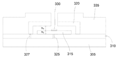
図3は、電子センサとして機能可能、酸化還元分子を検出可能、および/または酸化還元サイクル・センサとして機能可能な別のナノギャップ・トランスデューサを示している。図3において、基板305は、誘電体層310および第1の電極315を備える。第2の電極320は、高さh1のギャップを介して第1の電極から離隔している。本発明の実施形態において、ギャップの高さh1は、500nm未満すなわち10〜200nm、10〜150nm、または25〜150nmである。任意選択として、誘電体層310を貫通するビア等の電子的相互接続325および327は、基板305に収容された任意選択の電子機器(図示せず)との接続を提供している。本発明の実施形態において、基板305は、集積回路(IC)チップであって、たとえば電極315および320の駆動用、信号読み出し用、信号増幅用、ならびに/またはデータ出力用の電子機器を備える。基板は、たとえばガラス、不動態化金属、ポリマー、半導体、ポリジメチルシロキサン(PDMS)、および/または柔軟なエラストマ材等の他の材料であってもよい。基板が電子機器を収容していない実施形態においては、絶縁層310の表面に沿うか、または基板305を貫通して、電極315および320との電気的接続が延在していてもよいし、その他の構成であってもよい。
FIG. 3 shows another nanogap transducer that can function as an electronic sensor, detect redox molecules, and / or function as a redox cycle sensor. In FIG. 3, the
図3のナノギャップ・トランスデューサは、電極315上に配設された分子結合領域330を備える。分子結合領域330は、優先的に官能化可能な材料で構成されている。優先的に官能化可能な材料は、関心のあるリンカー分子または生体分子を結合または付着させるナノギャップ・トランスデューサの露出領域(動作条件下において液体と接触する表面領域)を含む材料の能力と比較して、優先的に関心のあるリンカー分子および/または生体分子を結合または付着可能な材料である。本発明の実施形態において、優先的に官能化可能な材料の領域330は二酸化ケイ素で構成されており、第2の誘電材料の層335は酸窒化ケイ素で構成されている。電極315および320が白金、パラジウム、金、炭素材料(たとえば、ダイヤモンド、黒鉛状炭素、または非晶質炭素等)、ニッケル、および/またはインジウム・スズ酸化物で構成されている場合、露出二酸化ケイ素領域(分子結合領域330)は、たとえばアミノプロピルトリエトキシシラン等のシランを用いて優先的に官能化可能であってもよい。本発明の別の実施形態において、分子結合領域330は、酸化ハフニウム、酸化アルミニウム、または酸化タンタルで構成されており、電極315および320が白金、パラジウム、金、炭素材料(たとえば、ダイヤモンド、黒鉛状炭素、または非晶質炭素等)、ニッケル、および/またはインジウム・スズ酸化物で構成されている場合は、たとえばアミノプロピルトリエトキシシラン等のシランを用いて優先的に官能化可能であってもよい。本発明の別の実施形態において、分子結合領域330は、金、白金、またはパラジウムで構成されており、電極315および320がダイヤモンド、黒鉛状炭素、または非晶質炭素等の炭素材料で構成されている場合は、チオール基(−SH)またはジスルフィド基(−S−S−)を含む分子により優先的に官能化可能であってもよい。優先的に官能化可能な材料330および誘電体層335については、その他の材料も可能である。
The nanogap transducer of FIG. 3 includes a molecular
本発明の実施形態において、分子結合領域330は、所望の分子を1つだけ結合可能な有効表面積(ナノギャップ空洞内の溶液に露出可能であるとともに分子と結合可能な表面積)を有する。本発明の実施形態において、分子結合領域330は、40nm2〜500,000nm2の有効表面積を有する。採用する分子結合領域330のサイズは、使用するリンカー分子のサイズ等の因子によって決まってもよい。分子結合領域330上の結合部位数はリンカー分子のサイズによって制限されるため、リンカー分子が大きくなると、分子結合領域330のサイズも大きくすることができる。別の実施形態において、分子結合領域330における分子付着反応の数は、ナノギャップ・トランスデューサのアレイの分子結合領域330への付着時におけるリンカー分子および/またはプローブ分子の溶液濃度によって制限されてもよい。分子結合領域330への付着率を原則100%とするには、ナノギャップ・トランスデューサの一部についてのみ、分子結合領域330に分子が1つだけ付着し、残りのトランスデューサについては、分子結合領域330に2つ以上の分子が付着するようにしてもよい。分子結合領域330当たりの分子数は、使用前の試験および/または分子結合領域330の単一分子と一致しない結果のフィルタリングによって決定してもよい。
In an embodiment of the present invention, the molecular
本発明の実施形態において、分子結合領域330は、リンカー分子、リンカー分子の組み合わせ、および/またはプローブ分子を含む。リンカー分子は、分子結合領域330の表面に付着していてもよく、関心のある分子(たとえば、プローブ分子または別のリンカー分子等)に付着可能な官能基を備える。また、リンカー分子は、分子結合領域330と選択的に反応する(ただし、誘電材料335または電極材料315および320とは反応しない)ように選択可能であって、たとえばシラン、チオール、ジスルフィド、イソチオシネート、アルケン、およびアルキン等の分子が挙げられる。プローブ分子は、たとえばDNA配列、RNA配列、ビオチンもしくはアビジン、ならびに抗体、受容体およびその特定の結合パートナー、タンパク質およびその特定の小分子結合パートナー、ならびに/またはペプチド等の関心のある標的分子と選択的に結合可能な分子である。プローブ分子は、1または複数の分子認識部位を含む。抗体としては、たとえばポリクローナル抗体およびモノクローナル抗体のほか、これら抗体の抗原結合フラグメントが挙げられる。抗体または抗体の抗原結合フラグメントは、たとえば検体のエピトープに対する特定の結合活性を有することを特徴とする。プローブは、たとえば抗原/抗体、ビオチン/アビジン、ホルモン/ホルモン受容体、二重鎖核酸、IgG/タンパク質A、ならびにDNA/DNAおよびDNA/RNA等のポリヌクレオチド対といった免疫学的な対等の特定の結合対のいずれかの要素であってもよい。また、プローブ分子は、既知のカップリング構造を介してリンカー分子とカップリングされていてもよい。
In embodiments of the invention, the molecular
電極315および320は、導電性材料で構成されている。本発明の実施形態において、電極315および320は、ダイヤモンド、白金、および/または金で構成されている。本発明の別の実施形態において、電極315および320は、パラジウム、ニッケル、黒鉛状炭素、非晶質炭素、および/またはインジウム・スズ酸化物で構成されている。本発明の実施形態において、少なくとも一方の電極315または320は、導電性ダイヤモンド材料で構成されている。本発明の実施形態において、電極315は、導電性ダイヤモンドで構成されている。本発明のさらに別の実施形態において、電極315および320はともに、導電性ダイヤモンド材料で構成されている。ダイヤモンドは、たとえばドーピングによって導電性を有するように作製してもよい。ドーパントとしては、たとえばホウ素、窒素、およびリンが挙げられる。本発明の一実施形態において、ドーパントはホウ素である。ホウ素をドープしたダイヤモンド材料のドーピング濃度としては、1020atoms/cm3より大きく1022atoms/cm3より小さな濃度が挙げられる。本発明の実施形態において、第1の電極315が導電性ダイヤモンド材料で構成されている場合、電極の高さh2は、200〜1000nmである。別の実施形態において、導電性ダイヤモンド電極の高さh2は、5〜25nmである。本発明の実施形態において、導電性ダイヤモンド膜は、マイクロ結晶またはナノ結晶ダイヤモンドである。動作時には通常、ナノギャップ・トランスデューサと併せて基準電極(図示せず)も使用する。基準電極は、測定対象ではあるがナノギャップ内に配置する必要のない溶液と接触する。
The
図4は、電子センサとして機能可能、酸化還元分子を検出可能、および/または酸化還元サイクル・センサとして機能可能なさらに別のナノギャップ・トランスデューサを示している。図4において、基板405は、誘電体層410および第1の電極415を備える。第2の電極420は、高さh1のギャップを介して第1の電極から離隔している。本発明の実施形態において、ギャップの高さh1は、500nm未満すなわち10〜200nm、10〜150nm、または25〜150nmである。任意選択として、誘電体層410を貫通するビア等の電子的相互接続425および427は、基板405に収容された任意選択の電子機器(図示せず)との接続を提供している。本発明の実施形態において、基板405は、集積回路(IC)チップであって、たとえば電極415および420の駆動用、信号読み出し用、信号増幅用、ならびに/またはデータ出力用の電子機器を備える。基板は、たとえばガラス、不動態化金属、ポリマー、半導体、PDMS(ポリジメチルシロキサン)、および/または柔軟なエラストマ材等の他の材料であってもよい。基板が電子機器を収容していない実施形態においては、絶縁層410の表面に沿うか、または基板405を貫通して、電極415および420との電気的接続が延在していてもよいし、その他の構成であってもよい。
FIG. 4 shows yet another nanogap transducer that can function as an electronic sensor, detect redox molecules, and / or function as a redox cycle sensor. In FIG. 4, the
図4のナノギャップ・トランスデューサは、電極415の孔に配設された分子結合領域430を備える。分子結合領域430は、優先的に官能化可能な材料で構成されている。優先的に官能化可能な材料は、関心のあるリンカー分子または生体分子を結合または付着させるナノギャップ・トランスデューサの露出領域(動作条件下において液体と接触する表面領域)を含む材料の能力と比較して、優先的に関心のあるリンカー分子および/または生体分子を結合または付着可能な材料である。分子結合領域430は、誘電体層410の露出領域または誘電体層410とは異なる優先的に官能化可能な材料の任意選択領域412を含んでいてもよい。優先的に官能化可能な材料の任意選択領域412は、第1の電極415の孔に近接して配置されており、優先的に官能化可能な材料の領域412の表面は、この電極の孔を介して露出している。優先的に官能化可能な材料を含む任意選択領域412は、その他の形状およびサイズを有していてもよく、誘電体領域410内または誘電体領域410の表面に凹設されていてもよい。本発明の実施形態において、優先的に官能化可能な材料の領域430は二酸化ケイ素で構成されており、第2の誘電材料の層435は酸窒化ケイ素で構成されている。電極415および420が白金、パラジウム、金、炭素材料(たとえば、ダイヤモンド、黒鉛状炭素、または非晶質炭素等)、ニッケル、および/またはインジウム・スズ酸化物で構成されている場合、露出二酸化ケイ素領域(分子結合領域430)は、たとえばアミノプロピルトリエトキシシラン等のシランを用いて優先的に官能化可能であってもよい。本発明の別の実施形態において、分子結合領域430は、酸化ハフニウム、酸化アルミニウム、または酸化タンタルで構成されており、電極415および420が白金、パラジウム、金、炭素材料(たとえば、ダイヤモンド、黒鉛状炭素、または非晶質炭素等)、ニッケル、および/またはインジウム・スズ酸化物で構成されている場合は、たとえばアミノプロピルトリエトキシシラン等のシランを用いて優先的に官能化可能であってもよい。本発明の別の実施形態において、分子結合領域430は、金、白金、またはパラジウムで構成されており、電極415および420がダイヤモンド、黒鉛状炭素、または非晶質炭素等の炭素材料で構成されている場合は、チオール基(−SH)またはジスルフィド基(−S−S−)を含む分子により優先的に官能化可能であってもよい。優先的に官能化可能な材料430および誘電体層435については、その他の材料も可能である。
The nanogap transducer of FIG. 4 includes a molecular
本発明の実施形態において、分子結合領域430は、所望の分子を1つだけ結合可能な有効表面積(ナノギャップ空洞内の溶液に露出可能であるとともに分子と結合可能な表面積)を有する。本発明の実施形態において、分子結合領域430は、40nm2〜500,000nm2の有効表面積を有する。採用する分子結合領域430のサイズは、使用するリンカー分子のサイズ等の因子によって決まってもよい。分子結合領域430上の結合部位数はリンカー分子のサイズによって制限されるため、リンカー分子が大きくなると、分子結合領域430のサイズも大きくすることができる。別の実施形態において、分子結合領域430における分子付着反応の数は、ナノギャップ・トランスデューサのアレイの分子結合領域430への付着時におけるリンカー分子および/またはプローブ分子の溶液濃度によって制限されてもよい。分子結合領域430への付着率を原則100%とするには、ナノギャップ・トランスデューサの一部についてのみ、分子結合領域430に分子が1つだけ付着し、残りのトランスデューサについては、分子結合領域430に2つ以上の分子が付着するようにしてもよい。分子結合領域330当たりの分子数は、使用前の試験および/または分子結合領域430の単一分子と一致しない結果のフィルタリングによって決定してもよい。
In an embodiment of the present invention, the molecular
本発明の実施形態において、分子結合領域430は、リンカー分子、リンカー分子の組み合わせ、および/またはプローブ分子を含む。リンカー分子は、分子結合領域430の表面に付着していてもよく、関心のある分子(たとえば、プローブ分子または別のリンカー分子等)に付着可能な官能基を備える。また、リンカー分子は、分子結合領域430と選択的に反応する(ただし、誘電材料435または電極材料415および420とは反応しない)ように選択可能であって、たとえばシラン、チオール、ジスルフィド、イソチオシネート、アルケン、およびアルキン等の分子が挙げられる。プローブ分子は、たとえばDNA配列、RNA配列、ビオチンもしくはアビジン、ならびに抗体、受容体およびその特定の結合パートナー、タンパク質およびその特定の小分子結合パートナー、ならびに/またはペプチド等の関心のある標的分子と選択的に結合可能な分子である。プローブ分子は、1または複数の分子認識部位を含む。抗体としては、たとえばポリクローナル抗体およびモノクローナル抗体のほか、これら抗体の抗原結合フラグメントが挙げられる。抗体または抗体の抗原結合フラグメントは、たとえば検体のエピトープに対する特定の結合活性を有することを特徴とする。プローブは、たとえば抗原/抗体、ビオチン/アビジン、ホルモン/ホルモン受容体、二重鎖核酸、IgG/タンパク質A、ならびにDNA/DNAおよびDNA/RNA等のポリヌクレオチド対といった免疫学的な対等の特定の結合対のいずれかの要素であってもよい。また、プローブ分子は、既知のカップリング構造を介してリンカー分子とカップリングされていてもよい。
In embodiments of the invention, the molecular
電極415および420は、導電性材料で構成されている。本発明の実施形態において、電極415および420は、ダイヤモンド、白金、および/または金で構成されている。本発明の別の実施形態において、電極415および420は、パラジウム、ニッケル、黒鉛状炭素、非晶質炭素、および/またはインジウム・スズ酸化物で構成されている。本発明の実施形態において、少なくとも一方の電極415または420は、導電性ダイヤモンド材料で構成されている。本発明の実施形態において、電極415は、導電性ダイヤモンドで構成されている。本発明のさらに別の実施形態において、電極415および420はともに、導電性ダイヤモンド材料で構成されている。ダイヤモンドは、たとえばドーピングによって導電性を有するように作製してもよい。ドーパントとしては、たとえばホウ素、窒素、およびリンが挙げられる。本発明の一実施形態において、ドーパントはホウ素である。ホウ素をドープしたダイヤモンド材料のドーピング濃度としては、1020atoms/cm3より大きく1022atoms/cm3より小さな濃度が挙げられる。本発明の実施形態において、第1の電極415が導電性ダイヤモンド材料で構成されている場合、電極の高さh2は、200〜1000nmである。別の実施形態において、導電性ダイヤモンド電極の高さh2は、5〜25nmである。本発明の実施形態において、導電性ダイヤモンド膜は、マイクロ結晶またはナノ結晶ダイヤモンドである。動作時には通常、ナノギャップ・トランスデューサと併せて基準電極(図示せず)も使用する。基準電極は、測定対象ではあるがナノギャップ内に配置する必要のない溶液と接触する。
The
図5Aおよび図5Bは、分子結合領域を有するナノギャップ・トランスデューサの作製方法を示している。図5Aにおいて、構造(i)は、基板505、誘電体層510、および第1の電極層515を備える。本発明の実施形態において、第1の電極層515は、導電性ダイヤモンド材料、白金、金、パラジウム、ニッケル、黒鉛状炭素、非晶質炭素、またはインジウム・スズ酸化物で構成されている。第1の電極層515が導電性ダイヤモンドで構成された実施形態においては、第1の電極層515上に硬質マスク層20が配設されている。導電性ダイヤモンド材料は、たとえばホット・フィラメント化学気相成長(chemical vapor deposition:CVD)、マイクロ波プラズマCVD、または燃焼炎アシストCVDプロセスによって堆積させてもよい。また、導電性ダイヤモンド材料は、たとえばダイヤモンド粒子を含む溶液に基板を浸して超音波処理により表面に粒子を付着させるか、または基板表面上で回転させる材料中にダイヤモンド粒子を懸濁することによって堆積させたシード層上に堆積させてもよい。本発明の実施形態において、導電性ダイヤモンド材料は、ホウ素をドープしたダイヤモンドである。本発明の実施形態において、導電性ダイヤモンド材料は、1020atoms/cm3より大きく1022atoms/cm3より小さなホウ素ドーピング濃度で堆積させる。本発明の実施形態において、硬質マスク層20は、たとえば二酸化クロムまたは二酸化ケイ素で構成されている。第1の電極層515が白金および/または金で構成された本発明の実施形態において、この白金および/または金は、その堆積前にフォトレジスト層を堆積・パターニングした後、フォトレジストをリフトオフして不要な領域の白金および/または金を除去するリフトオフ・プロセスを用いたスパッタリングおよびパターニングによって堆積させてもよい。本発明の実施形態において、基板505は、たとえば電極駆動用、信号検出用、信号増幅用、および/またはデータ出力用の電子機器を備えたICチップである。また、任意選択として、導電性ビア525および530が誘電体層510を貫通して基板505まで設けられており、電極と基板505に収容された任意選択の電子機器とを相互接続する。基板505については、その他の材料も可能である。
5A and 5B illustrate a method for making a nanogap transducer having a molecular binding region. In FIG. 5A, structure (i) includes a
本発明の実施形態において、第1の電極515が導電性ダイヤモンド材料で構成されている場合は、上下電極間の短絡の可能性を最小限に抑えるため、第1の電極の厚さを最小化するのが望ましいことが分かっている。また、第1の電極のアスペクト比が高くなると、電極の縁部において犠牲コンフォーマル・コーティングが薄くなってしまうことが分かっている。ただし、マイクロ結晶ダイヤモンド材料の表面粗度が過大にならないように第1の電極の高さを最小化することが必要であることも分かっている。第1の電極の表面粗度が過大になると、犠牲コンフォーマル・コーティングにおいて開口が発生し、第1および第2の電極間で短絡が発生する可能性があることが分かっている。本発明の実施形態において、第1の電極が導電性ダイヤモンドで構成されている場合は、高さの最小化および表面粗度に関する要件が釣り合うように、第1の電極の高さが200〜1000nm、300〜800nm、350〜700nmであってもよい。
In an embodiment of the present invention, when the
図5Aの構造(ii)は、硬質マスク層520をパターニングし、不要領域の硬質マスク層520を除去し、露出したダイヤモンド電極層515をエッチングすることによって作成してもよい。露出したダイヤモンド電極層515のエッチングは、たとえば酸素プラズマを用いて行ってもよい。この酸素プラズマによるエッチングは、たとえば70〜100Cまで温度を上げると容易になる可能性がある。その後、硬質マスク層520を除去する。
The structure (ii) of FIG. 5A may be created by patterning the
犠牲材料のコンフォーマル膜535を堆積させてパターニングすると、図5Aの構造(iii)が得られる。犠牲材料のコンフォーマル膜535のパターニングは、まずフォトレジストを堆積させ、フォトレジストをパターニングし、たとえばスパッタリングまたは原子層成長(atomic layer deposition:ALD)によって犠牲材料を堆積させ、フォトレジストをリフトオフして所望の領域に犠牲材料のコンフォーマル膜を画成する(リフトオフ・プロセス)ことにより行ってもよい。本発明の実施形態において、犠牲材料は、クロムまたはタングステンを含む。犠牲材料のコンフォーマル膜535は、たとえばスパッタリングALDによって堆積させることにより、下部電極515を包み込む膜を実現するようにしてもよい。本発明の実施形態において、犠牲材料の薄膜535は、500nm未満すなわち10〜200nm、10〜150nm、または25〜150nmの厚さを有する。
A sacrificial material
犠牲材料のコンフォーマル膜535上に第2の電極材料540を堆積させてパターニングすると、図5Aの構造(iv)が得られる。第2の電極材料540は、リフトオフ・プロセスを用いてリソグラフィによりパターニングを行ってもよい。本発明の実施形態において、第2の電極材料540は、導電性ダイヤモンドである。導電性ダイヤモンドは、ホット・フィラメントCVD、マイクロ波プラズマCVD、または燃焼炎アシストCVDプロセスを用いてシード層形成および層堆積を行うことにより堆積させてもよい。本発明の実施形態において、第2の電極540の材料がダイヤモンドである場合、犠牲材料のコンフォーマル膜535はタングステンを含む。本発明のさらに別の実施形態において、第2の電極540は、白金、金、ニッケル、パラジウム、黒鉛状炭素、非晶質炭素、またはインジウム・スズ酸化物で構成されている。白金電極は、たとえば接着層として薄いクロム層(およそ10nmの厚さ)をスパッタリングした後、白金層をスパッタリングすることによって堆積させてもよい。金電極材料は、たとえばスパッタリング、蒸着、電着、または無電解析出プロセスによって堆積させてもよい。本発明の実施形態において、第2の電極540が金で構成されている場合、犠牲材料535はタングステンである。
When the
その後、図5Aの構造(iv)上に第2の誘電体層545、優先的に官能化可能な材料の層550、および第3の誘電材料の層555を堆積させると、図5Bの構造(v)が得られる。第2および第3の層545および555の誘電材料は、たとえば酸窒化ケイ素であってもよく、優先的に官能化可能な材料の層550は二酸化ケイ素であってもよい。別の実施形態において、第2および第3の層545および555の誘電材料は、たとえば窒化ケイ素であってもよく、優先的に官能化可能な材料の層550は、金、白金、またはパラジウムであってもよい。そして、第2の誘電体層545、優先的に官能化可能な材料の層550、および第3の誘電材料の層555を貫通して、アクセス孔560を作成する。アクセス孔560は、フォトレジスト・マスクを用いてリソグラフィにより孔を画成した後、ドライ・エッチング・プロセスにより孔を形成することによって作成してもよい。そして、犠牲材料535を除去して、第1および第2の電極515および540間にギャップを作成する。犠牲材料535がタングステンまたはクロムである実施形態においては、たとえばウェット・エッチングにより犠牲材料535を除去してもよい。得られる構造を図5Bの(vi)に示す。本発明の実施形態において、ギャップの高さh1は、500nm未満すなわち10〜200nm、10〜150nm、または25〜150nmである。
A
図6Aおよび図6Bは、分子結合領域を有するナノギャップ・トランスデューサの別の作製方法を示している。図6Aにおいて、構造(i)は、基板605、誘電体層610、および第1の電極615を備える。本発明の実施形態において、第1の電極615は、導電性ダイヤモンド材料、白金、金、パラジウム、ニッケル、黒鉛状炭素、非晶質炭素、またはインジウム・スズ酸化物で構成されている。本発明の実施形態において、導電性ダイヤモンド材料は、ホウ素をドープしたダイヤモンドである。本発明の実施形態において、導電性ダイヤモンド材料は、1020atoms/cm3より大きく1022atoms/cm3より小さなホウ素ドーピング濃度で堆積させる。本発明の実施形態において、基板605は、たとえば電極駆動用、信号検出用、信号増幅用、および/またはデータ出力用の電子機器を備えたICチップである。また、任意選択として、導電性ビア625および630が誘電体層610を貫通して基板605まで設けられており、電極と基板605に収容された任意選択の電子機器とを相互接続する。基板605については、その他の材料も可能である。第1の電極615上には、優先的に官能化可能な材料で構成された分子結合領域620が配設されている。任意選択として、分子結合領域620と電極615との間には、接着層623が存在する。接着層623は、窒化ケイ素で構成されており、CVDによって堆積させてもよい。分子結合領域620は、たとえばCVDにより堆積させ、フォトリソグラフィによりパターニングを行ってもよい。本発明の実施形態において、分子結合領域620は、40nm2〜500,000nm2の露出表面積を有する。
6A and 6B show another method for making a nanogap transducer having a molecular binding region. In FIG. 6A, structure (i) comprises a
本発明の実施形態において、第1の電極615が導電性ダイヤモンド材料で構成されている場合は、上下電極間の短絡の可能性を最小限に抑えるため、第1の電極の厚さを最小化するのが望ましいことが分かっている。また、第1の電極のアスペクト比が高くなると、電極の縁部において犠牲コンフォーマル・コーティングが薄くなってしまうことが分かっている。ただし、マイクロ結晶ダイヤモンド材料の表面粗度が過大にならないように第1の電極の高さを最小化することが必要であることも分かっている。第1の電極の表面粗度が過大になると、犠牲コンフォーマル・コーティングにおいて開口が発生し、第1および第2の電極間で短絡が発生する可能性があることが分かっている。本発明の実施形態において、第1の電極が導電性ダイヤモンドで構成されている場合は、高さの最小化および表面粗度に関する要件が釣り合うように、第1の電極の高さが200〜1000nm、300〜800nm、350〜700nmであってもよい。
In an embodiment of the present invention, when the
図6Aの構造(ii)は、図6Aの構造(i)上に犠牲材料のコンフォーマル膜635を堆積させてパターニングすることにより作成してもよい。犠牲材料のコンフォーマル膜635のパターニングは、まずフォトレジストを堆積させ、フォトレジストをパターニングし、たとえばスパッタリングまたは原子層成長(ALD)によって犠牲材料を堆積させ、フォトレジストをリフトオフして所望の領域に犠牲材料のコンフォーマル膜を画成する(リフトオフ・プロセス)ことにより行ってもよい。本発明の実施形態において、犠牲材料は、クロムまたはタングステンを含む。犠牲材料のコンフォーマル膜635は、たとえばスパッタリングALDによって堆積させることにより、下部電極615を包み込む膜を実現するようにしてもよい。本発明の実施形態において、犠牲材料の薄膜635は、500nm未満すなわち10〜200nm、10〜150nm、または25〜150nmの厚さを有する。
The structure (ii) of FIG. 6A may be created by depositing and patterning a
犠牲材料のコンフォーマル膜635上に第2の電極640の材料を堆積させてパターニングすると、図6Aの構造(iii)が得られる。第2の電極640の材料は、リフトオフ・プロセスを用いてリソグラフィによりパターニングを行ってもよい。本発明の実施形態において、第2の電極640の材料は、導電性ダイヤモンドである。導電性ダイヤモンドは、ホット・フィラメントCVD、マイクロ波プラズマCVD、または燃焼炎アシストCVDプロセスを用いてシード層形成および層堆積を行うことにより堆積させてもよい。本発明の実施形態において、第2の電極640の材料がダイヤモンドである場合、犠牲材料のコンフォーマル膜635はタングステンを含む。本発明のさらに別の実施形態において、第2の電極640は、白金、金、ニッケル、パラジウム、黒鉛状炭素、非晶質炭素、またはインジウム・スズ酸化物で構成されている。白金電極は、たとえば接着層として薄いクロム層(およそ10nmの厚さ)をスパッタリングした後、白金層をスパッタリングすることによって堆積させてもよい。金電極材料は、たとえばスパッタリング、蒸着、電着、または無電解析出プロセスによって堆積させてもよい。本発明の実施形態において、第2の電極640が金で構成されている場合、犠牲材料635はタングステンである。
When the material of the
その後、図6Aの構造(iii)上に第2の誘電体層645を堆積させると、図6Bの構造(iv)が得られる。第2の層645の誘電材料は、たとえば酸窒化ケイ素であってもよく、分子結合領域620の優先的に官能化可能な材料は二酸化ケイ素であってもよい。別の実施形態において、第2の層645の誘電材料は、たとえば二酸化ケイ素、窒化ケイ素、または酸窒化ケイ素であってもよく、優先的に官能化可能な材料は、金、白金、またはパラジウムであってもよい。そして、第2の誘電体層645を貫通して、アクセス孔650を作成すると、図6Bの構造(v)が得られる。アクセス孔650は、フォトレジスト・マスクを用いてリソグラフィにより孔を画成した後、ドライ・エッチング・プロセスにより孔を形成することによって作成してもよい。そして、犠牲材料635を除去して、第1および第2の電極615および640間にギャップを作成する。犠牲材料635がタングステンまたはクロムである実施形態においては、たとえばウェット・エッチングにより犠牲材料635を除去してもよい。得られる構造を図6Bの(vi)に示す。本発明の実施形態において、第1および第2の電極615および640間のギャップの高さは、500nm未満すなわち10〜200nm、10〜150nm、または25〜150nmである。
Thereafter, a
図7Aおよび図7Bは、分子結合領域を有するナノギャップ・トランスデューサのさらに別の作製方法を示している。図7Aにおいて、構造(i)は、基板705、誘電体層710、および優先的に官能化可能な材料の任意選択の領域720を備える。本発明の実施形態において、基板705は、たとえば電極駆動用、信号検出用、信号増幅用、および/またはデータ出力用の電子機器を備えたICチップである。また、任意選択として、導電性ビア725および730が誘電体層710を貫通して基板705まで設けられており、電極と基板705に収容された任意選択の電子機器とを相互接続する。基板705については、その他の材料も可能である。
7A and 7B show yet another method for fabricating a nanogap transducer having a molecular binding region. In FIG. 7A, structure (i) comprises a
図7Aの構造(ii)は、第1の電極715の材料を堆積させてパターニングすることにより作成してもよい。このパターニングにより、分子結合領域723が露出した孔が第1の電極715内に形成される。本発明の実施形態において、分子結合領域723は、40nm2〜500,000nm2の露出表面積を有する。本発明の実施形態において、第1の電極715は、導電性ダイヤモンド材料、白金、金、ニッケル、パラジウム、黒鉛状炭素、非晶質炭素、またはインジウム・スズ酸化物で構成されている。本発明の実施形態において、導電性ダイヤモンド材料は、ホウ素をドープしたダイヤモンドである。本発明の実施形態において、導電性ダイヤモンド材料は、1020atoms/cm3より大きく1022atoms/cm3より小さなホウ素ドーピング濃度で堆積させる。導電性ダイヤモンドは、たとえばホット・フィラメントCVD、マイクロ波プラズマCVD、または燃焼炎アシストCVDプロセスを用いてシード層形成および層堆積を行うことにより堆積させてもよい。また、導電性ダイヤモンド材料は、硬質マスクを用いてパターニングを行ってもよい。白金電極は、たとえばスパッタリングにより堆積させてもよい。金電極材料は、たとえばスパッタリング、蒸着、電着、または無電解析出プロセスによって堆積させてもよい。白金または金で構成された第1の電極715は、リフトオフ・プロセスを用いてリソグラフィによりパターニングを行ってもよい。
The structure (ii) of FIG. 7A may be created by depositing and patterning the material of the
本発明の実施形態において、第1の電極715が導電性ダイヤモンド材料で構成されている場合は、上下電極間の短絡の可能性を最小限に抑えるため、第1の電極の厚さを最小化するのが望ましいことが分かっている。また、第1の電極のアスペクト比が高くなると、電極の縁部において犠牲コンフォーマル・コーティングが薄くなってしまうことが分かっている。ただし、マイクロ結晶ダイヤモンド材料の表面粗度が過大にならないように第1の電極の高さを最小化することが必要であることも分かっている。第1の電極の表面粗度が過大になると、犠牲コンフォーマル・コーティングにおいて開口が発生し、第1および第2の電極間で短絡が発生する可能性があることが分かっている。本発明の実施形態において、第1の電極が導電性ダイヤモンドで構成されている場合は、高さの最小化および表面粗度に関する要件が釣り合うように、第1の電極の高さが200〜1000nm、300〜800nm、350〜700nmであってもよい。
In an embodiment of the present invention, when the
図7Aの構造(iii)は、図7Aの構造(ii)上に犠牲材料のコンフォーマル膜735を堆積させてパターニングすることにより作成してもよい。犠牲材料のコンフォーマル膜735のパターニングは、まずフォトレジストを堆積させ、フォトレジストをパターニングし、たとえばスパッタリングまたは原子層成長(ALD)によって犠牲材料を堆積させ、フォトレジストをリフトオフして所望の領域に犠牲材料のコンフォーマル膜を画成する(リフトオフ・プロセス)ことにより行ってもよい。本発明の実施形態において、犠牲材料は、クロムまたはタングステンを含む。犠牲材料のコンフォーマル膜735は、たとえばスパッタリングALDによって堆積させることにより、下部電極715を包み込む膜を実現するようにしてもよい。本発明の実施形態において、犠牲材料の薄膜735は、500nm未満すなわち10〜200nm、10〜150nm、または25〜150nmの厚さを有する。
The structure (iii) of FIG. 7A may be created by depositing and patterning a
犠牲材料のコンフォーマル層735上に第2の電極材料740を堆積させてパターニングすると、図7Bの構造(iv)が得られる。本発明の実施形態において、第2の電極740は、導電性ダイヤモンド、白金、金、ニッケル、パラジウム、黒鉛状炭素、非晶質炭素、またはインジウム・スズ酸化物で構成されている。本発明の実施形態において、第2の電極材料は、導電性ダイヤモンドである。導電性ダイヤモンドは、ホット・フィラメントCVD、マイクロ波プラズマCVD、または燃焼炎アシストCVDプロセスを用いてシード層形成および層堆積を行うことにより堆積させてもよい。また、導電性ダイヤモンド材料は、硬質マスクを用いてパターニングを行ってもよい。本発明の実施形態において、第2の電極740の材料がダイヤモンドである場合、犠牲材料のコンフォーマル膜735はタングステンを含む。本発明のさらに別の実施形態において、第2の電極740は、白金または金で構成されている。白金電極は、たとえば接着層として薄いクロム層(およそ10nmの厚さ)をスパッタリングした後、白金層をスパッタリングすることによって堆積させてもよい。金電極材料は、たとえばスパッタリング、蒸着、電着、または無電解析出プロセスによって堆積させてもよい。本発明の実施形態において、第2の電極740が金で構成されている場合、犠牲材料735はタングステンである。白金または金で構成された第2の電極740は、リフトオフ・プロセスを用いてリソグラフィによりパターニングを行ってもよい。
A
その後、図7Aの構造(iv)上に第2の誘電体層745を堆積させてパターニングを行うと、図7Bの構造(v)が得られる。第2の層745の誘電材料は、たとえば酸窒化ケイ素であってもよく、分子結合領域723の優先的に官能化可能な材料は二酸化ケイ素であってもよい。別の実施形態において、第2の層745の誘電材料は、たとえば二酸化ケイ素、窒化ケイ素、または酸窒化ケイ素であってもよく、優先的に官能化可能な材料は、金、白金、またはパラジウムであってもよい。このパターニングによって、第2の誘電体層745を貫通するアクセス孔750が形成される。アクセス孔750は、フォトレジスト・マスクを用いてリソグラフィにより孔を画成した後、ドライ・エッチング・プロセスにより孔を形成することによって作成してもよい。そして、犠牲材料735を除去して、図7Bの構造(vi)が得られる。犠牲材料735がタングステンまたはクロムである実施形態においては、たとえばウェット・エッチングにより犠牲材料735を除去してもよい。本発明の実施形態において、第1および第2の電極715および740間のギャップの高さは、500nm未満すなわち10〜200nm、10〜150nm、または25〜150nmである。
Thereafter, when the
表面を改変して分子付着を向上させる場合に利用可能なシラン分子は、電極に用いる材料に応じて、たとえばX3−Si−YR”、X3−Si−(N)YR”、およびX3−Si−(N2)YR”という化学式であってもよい。ここで、Xは、たとえば−Cl、−OCH3、または−OCH2CH3等の脱離基である。R”は、たとえば−NH2、−COOH、−COH、−CHCH2、または−SH等の反応カップリング基である。Nは、たとえばアルキル基等の非反応基である。カップリングする表面付着シラン分子が提供する有機基は、たとえばカルボキシル基、アルデヒド、エステル、アルケン、アルキン、チオール、イソシアネート、イソチオシアネート、置換アミン、エポキシド、ビオチン等の小分子、またはアルコールであってもよい。一般的に、Yは、1〜16個の炭素原子を有する炭化水素等の非反応基である。−YR”の例としては、−(CH2)3NH2、−(CH2)2COOH、および−(CH2)2SH等が挙げられる。シランの例としては、3−アミノプロピルトリエトキシシラン(aminopropyltriethoxysilane:APTS)、メルカプトシラン、およびグリシドキシトリメトキシシラン(エポキシド反応カップリング基を有する)等が挙げられる。その他の官能基およびシランも可能である。シラン化する表面は、たとえば溶液またはシランガスとしてのシラン分子と反応させてもよい。 Silane molecules that can be used when modifying the surface to improve molecular adhesion include, for example, X 3 —Si—YR ″, X 3 —Si— (N) YR ″, and X 3 depending on the material used for the electrode. The chemical formula may be —Si— (N 2 ) YR ″, where X is a leaving group such as —Cl, —OCH 3 , or —OCH 2 CH 3. R ″ is, for example, A reaction coupling group such as —NH 2 , —COOH, —COH, —CHCH 2 , or —SH. N is a non-reactive group such as an alkyl group. The organic groups provided by the surface-attached silane molecules to be coupled may be, for example, carboxyl groups, aldehydes, esters, alkenes, alkynes, thiols, isocyanates, isothiocyanates, substituted amines, epoxides, biotin and other small molecules, or alcohols. Good. Generally, Y is a non-reactive group such as a hydrocarbon having 1 to 16 carbon atoms. Examples of —YR ″ include — (CH 2 ) 3 NH 2 , — (CH 2 ) 2 COOH, — (CH 2 ) 2 SH, etc. Examples of silane include 3-aminopropyltriethoxy Examples include silane (aminopropyltrisilane: APTS), mercaptosilane, and glycidoxytrimethoxysilane (having an epoxide reactive coupling group), etc. Other functional groups and silanes are also possible. You may make it react with the silane molecule | numerator as silane gas.
また、誘電材料としては、たとえば二酸化ケイ素、窒化ケイ素、酸窒化ケイ素、炭素ドープ酸化物(carbon doped oxide:CDO)、炭化ケイ素、パーフルオロシクロブタンもしくはポリテトラフルオロエチレン等の有機ポリマー、フルオロケイ酸塩ガラス(fluorosilicate glass:FSG)、ならびに/またはシルセスキオキサン、シロキサン、もしくは有機ケイ酸塩ガラス等の有機シリケート等が挙げられる。また、有機材料は、たとえばポリイミド等のポリマーであってもよい。 Examples of the dielectric material include silicon dioxide, silicon nitride, silicon oxynitride, carbon doped oxide (CDO), silicon carbide, organic polymers such as perfluorocyclobutane or polytetrafluoroethylene, and fluorosilicates. Examples thereof include glass (fluorosilicate glass: FSG) and / or organic silicates such as silsesquioxane, siloxane, or organosilicate glass. The organic material may be a polymer such as polyimide.
導電性ダイヤモンド電極を用いるとバックグラウンド電流が小さくなることが分かっているため、2つの作動電極の一方のみを用いて少数の分子の測定結果を記録することができる。測定結果の記録は、1つの分子だけであってもよい。別の実施形態においては、両電極において記録した測定結果を用いて信号を生成する。ナノギャップ・トランスデューサにおける電極電位および電流の測定および記録を行うシステムは、たとえばバイポテンショスタットを備える。バイポテンショスタットを用いることにより、溶液の電位に対する両電極の電位を制御するとともに、電極を流れる電流を測定する。電極を駆動して電流の測定および記録を行うシステムの部品の一部または全部は、集積回路(IC)チップ上に収容された個別にアドレス可能なナノギャップ・トランスデューサのアレイに電気的に結合された当該ICチップ内に配置されていてもよい。本発明の実施形態において、個別にアドレス可能なナノギャップ・トランスデューサと関連するコンピュータ・システムは、導電性ダイヤモンドで構成された1つの電極のみでの測定結果を用いて電極電位および電流値の測定および記録を行うソフトウェアを備える。別の実施形態において、このコンピュータ・システムは、2つの電極ならびに/または2つの電極および1つの電極の両者での電極電位の測定および記録を行うソフトウェアを備える。また、電気化学的相関分光法等の技術を用いることにより、ナノギャップ・デバイスにおいて逆バイアスをかけた2つの電極での測定結果から信号を生成するようにしてもよい。 Since it has been found that using a conductive diamond electrode reduces the background current, only one of the two working electrodes can be used to record the measurement results for a small number of molecules. The measurement result may be recorded for only one molecule. In another embodiment, the measurement results recorded at both electrodes are used to generate a signal. A system for measuring and recording electrode potential and current in a nanogap transducer comprises, for example, a bipotentiostat. By using a bipotentiostat, the potential of both electrodes relative to the potential of the solution is controlled, and the current flowing through the electrodes is measured. Some or all of the parts of the system that drive electrodes to measure and record current are electrically coupled to an array of individually addressable nanogap transducers housed on an integrated circuit (IC) chip. It may be arranged in the IC chip. In an embodiment of the present invention, a computer system associated with an individually addressable nanogap transducer can measure and measure electrode potentials and current values using measurements from only one electrode composed of conductive diamond. Software for recording is provided. In another embodiment, the computer system comprises software that measures and records the electrode potential at two electrodes and / or both the two electrodes and one electrode. Further, by using a technique such as electrochemical correlation spectroscopy, a signal may be generated from the measurement results of two electrodes that are reverse-biased in a nanogap device.
一般的に、ナノギャップ・トランスデューサ等の電極を用いた電子センサは、電極表面上またはその近傍に配置された材料のインピーダンス、抵抗、容量、および/または酸化還元電位を測定可能である。また、ナノギャップ・トランスデューサを載置する基板は、検出および/または駆動回路、スイッチング・ロジック、ラッチ、メモリ、および/または入出力装置を備えていてもよい。任意選択として、電極のセンシングおよび駆動ならびにデータの記録を行う電子機器の一部または全部は、ナノギャップ・トランスデューサのアレイを収容した基板の一部をなす集積回路である。また、任意選択として、入出力制御を提供する電子機器は、基板の集積回路チップ等に収容されるか、または基板外部の回路により提供される。さらに、任意選択として、ナノギャップ・トランスデューサのアレイには、電極への個別アドレス、選択電圧での電極駆動、電極に供給する電圧電流情報を格納するメモリ、電極特性を測定するメモリおよびマイクロプロセッサ、差動増幅器、電流検出回路(CMOS画像センサに用いる回路の変異形を含む)、ならびに/または電界効果トランジスタ(ダイレクト・フローティング・ゲート)の回路が備わっている。あるいは、外部機器および/または付属のコンピュータ・システムによって、これら機能のうちの1または複数を実行するようにしてもよい。 In general, an electronic sensor using an electrode such as a nanogap transducer can measure the impedance, resistance, capacitance, and / or redox potential of a material disposed on or near the electrode surface. The substrate on which the nanogap transducer is mounted may also include detection and / or drive circuitry, switching logic, latches, memory, and / or input / output devices. Optionally, some or all of the electronics that sense and drive the electrodes and record data are integrated circuits that form part of a substrate containing an array of nanogap transducers. Also, as an option, the electronic device that provides input / output control is housed in an integrated circuit chip or the like on the substrate, or provided by a circuit outside the substrate. Further, optionally, the array of nanogap transducers includes individual addresses to the electrodes, electrode drive at selected voltages, memory for storing voltage current information supplied to the electrodes, memory and microprocessor for measuring electrode characteristics, A differential amplifier, a current detection circuit (including a variant of a circuit used in a CMOS image sensor), and / or a field effect transistor (direct floating gate) circuit are provided. Alternatively, one or more of these functions may be executed by an external device and / or an attached computer system.
酸化還元サイクル測定においては、逆バイアスをかけた電極を用いて溶液中の酸化還元活性分子の荷電状態を繰り返し反転させることにより、各酸化還元活性分子が複数の酸化還元反応に参加することによって、複数の電子による電流値を測定する。酸化還元サイクル測定において、電極間のギャップの高さは、ナノメートルのオーダーである。2つの電極間の空洞内の酸化還元活性分子は、電極間で複数の電子を往復させるため、測定された電気化学的電流が増幅される。酸化還元活性種からの信号は、酸化還元種の安定性および酸化還元種の検出領域からの拡散能力等の因子に応じて、100倍より大きく増幅可能であってもよい。 In the redox cycle measurement, each redox active molecule participates in multiple redox reactions by repeatedly reversing the charge state of the redox active molecule in the solution using a reverse biased electrode. The current value by a plurality of electrons is measured. In the redox cycle measurement, the height of the gap between the electrodes is on the order of nanometers. Since the redox active molecule in the cavity between the two electrodes reciprocates a plurality of electrons between the electrodes, the measured electrochemical current is amplified. The signal from the redox active species may be able to be amplified more than 100 times depending on factors such as the stability of the redox species and the ability to diffuse from the redox species detection region.
本発明の実施形態において、ナノギャップ・トランスデューサの電極は、検出する酸化還元種の酸化・還元電位となるように独立してバイアスをかける。酸化還元種は電荷シャトルとして作用し、一方の電極から他方の電極へ分子が拡散すると、酸化還元分子が還元・酸化して、正味の電荷移動が生じる。両電極を流れる電流の大きさは、空洞内の検体(酸化還元種)の濃度に比例する。任意選択として、電極間のギャップは、ビーズで封止することにより、空洞からの酸化還元活性種の拡散を阻止することによって、酸化還元種の有効濃度を向上させる。空洞を封止すると、センサ測定時における空洞からの酸化還元種の漏れを防止できる。 In an embodiment of the invention, the electrodes of the nanogap transducer are independently biased to be at the oxidation / reduction potential of the redox species to be detected. The redox species acts as a charge shuttle. When molecules diffuse from one electrode to the other, the redox molecules are reduced and oxidized, resulting in a net charge transfer. The magnitude of the current flowing through both electrodes is proportional to the concentration of the analyte (redox species) in the cavity. Optionally, the gap between the electrodes is sealed with beads to improve the effective concentration of redox species by preventing the diffusion of redox active species from the cavity. Sealing the cavity can prevent redox species from leaking from the cavity during sensor measurement.
一般的に、酸化還元活性種は、複数回にわたって酸化および/または還元の状態を可逆的にサイクル可能な分子である。 In general, a redox-active species is a molecule capable of reversibly cycling oxidation and / or reduction states multiple times.
本発明の実施形態において、ナノギャップ・トランスデューサは、個別にアドレス可能なナノギャップ・トランスデューサのアレイであってもよい。アレイは、様々な寸法および個数のナノギャップ・トランスデューサで構築する。ナノギャップ・トランスデューサの個数割り付けの選択は、たとえば検出する検体の種類および個数、検出領域のサイズ、ならびにアレイの製造に伴うコスト等の因子によって決まる。たとえば、ナノギャップ・トランスデューサのアレイは、10×10、100×100、1,000×1,000、105×105、および106×106である。アレイは、超高密度、高密度、中密度、低密度、または超低密度に形成可能である。超高密度アレイの範囲としては、およそ1億〜10億個のセンサ/アレイである。高密度アレイの範囲としては、およそ百万〜1億個のセンサである。中密度アレイの範囲としては、およそ1万〜十万個のセンサである。低密度アレイは一般的に、1万個未満の空洞である。超低密度アレイは、千個未満のセンサである。 In embodiments of the invention, the nanogap transducer may be an array of individually addressable nanogap transducers. The array is constructed with nano-gap transducers of various sizes and numbers. The selection of the number of nanogap transducers depends on factors such as, for example, the type and number of analytes to be detected, the size of the detection area, and the cost associated with manufacturing the array. For example, arrays of nanogap transducers are 10 × 10, 100 × 100, 1,000 × 1,000, 10 5 × 10 5 , and 10 6 × 10 6 . Arrays can be formed in ultra-high density, high density, medium density, low density, or ultra-low density. The range of ultra high density arrays is approximately 100 to 1 billion sensors / arrays. The range of the high density array is approximately 1 million to 100 million sensors. The range of the medium density array is approximately 10,000 to 100,000 sensors. A low density array is typically less than 10,000 cavities. An ultra-low density array is less than a thousand sensors.
個別にアドレス可能なナノギャップ・トランスデューサのアレイは、ICチップ上に収容され、電気的に結合されていてもよい。ICチップは通常、ダイシングにより切り離して個別のICチップを生成する半導体ウェハ等の半導体基板上に構築する。ICチップを構築するベース基板は通常、シリコン・ウェハである。ただし、本発明の実施形態は、使用する基板の種類によって左右されるものではない。また、基板は、ゲルマニウム、アンチモン化インジウム、テルル化鉛、ヒ化インジウム、リン化インジウム、ヒ化ガリウム、アンチモン化ガリウム、および/またはその他のIII−V族材料が単独で構成されていてもよいし、ケイ素もしくは二酸化ケイ素との組み合わせで構成されていてもよいし、またはその他の絶縁材料で構成されていてもよい。また、各層および装置を含む各層は、本発明の実施形態を収容または製造する基板または基板の一部として特徴付けてもよい。 An array of individually addressable nanogap transducers may be housed on the IC chip and electrically coupled. IC chips are usually built on a semiconductor substrate such as a semiconductor wafer that is separated by dicing to produce individual IC chips. The base substrate on which the IC chip is built is usually a silicon wafer. However, the embodiment of the present invention does not depend on the type of substrate used. In addition, the substrate may be composed of germanium, indium antimonide, lead telluride, indium arsenide, indium phosphide, gallium arsenide, gallium antimonide, and / or other group III-V materials alone. It may be composed of a combination with silicon or silicon dioxide, or may be composed of other insulating materials. Also, each layer, including each layer and device, may be characterized as a substrate or part of a substrate that houses or manufactures embodiments of the present invention.
ナノギャップ・トランスデューサのアレイによれば、たとえば多数の固定化DNA分子の配列を同時に決定可能となる。ただし、その他の用途も可能である。固定化DNA分子は、配列決定するサンプルであってもよいし、配列が既知の捕捉DNAプローブを最初に固定化した後、配列決定するサンプルを固定化プローブに交雑してもよい。捕捉プローブは、サンプルDNAの一部に交雑するように設計された配列を有する。本発明の実施形態において、固定化するDNAフラグメント(または捕捉プローブ)は、各センサが統計上、固定化されたDNA分子を1つ有するように希釈する。配列情報は、固定化されたDNA分子を1つだけ有するナノギャップ・トランスデューサから組み立てる。不明瞭な結果を示すナノギャップ・トランスデューサからの情報は、無視してもよい。 An array of nanogap transducers can, for example, determine the sequence of many immobilized DNA molecules simultaneously. However, other uses are possible. The immobilized DNA molecule may be a sample to be sequenced, or a sample to be sequenced may be crossed to the immobilized probe after first immobilizing a capture DNA probe of known sequence. The capture probe has a sequence designed to hybridize to a portion of the sample DNA. In an embodiment of the invention, the DNA fragment (or capture probe) to be immobilized is diluted such that each sensor statistically has one immobilized DNA molecule. The sequence information is assembled from a nanogap transducer having only one immobilized DNA molecule. Information from nanogap transducers that show ambiguous results may be ignored.
核酸サンプルの増幅(すなわち、サンプル中の核酸分子のコピー数の増加)を任意選択として行わなくてもよい核酸の配列決定方法を提供する。図8は、核酸分子の配列決定、一塩基変異多型(single nucleotide polymorphism:SNP)の検出、および遺伝子発現の検出に有用な方法を記述したフロー図を示している。図8において、核酸分子は、電子センサ内部の表面に付着する。そして、標的核酸の一部に対して相補的なプライマを含むセンサ空洞に溶液を供給する。プライマDNA分子は、空洞内部に付着したDNA分子の一部に交雑し、付着したDNA分子について、DNAの相補鎖の合成の準備をする。空洞内部のDNAの配列が既知でない場合、プライマは、センサ内部のDNA鎖に提供されたランダム配列を有する多くのうちの1つと考えられる。また、プライマは、ヌクレアーゼ耐性ヌクレオチドで末端処理してもよい。空洞内部のDNA分子に対するプライマの交雑が可能となったら、DNAポリメラーゼ酵素および酸化還元中心改変(redox−center modified)ヌクレオチド三リン酸(nucleotide triphosphate:NTPまたはdNTP)を添加する。dNTPは、酸化還元改変デオキシアデノシン三リン酸(deoxyadenosine triphosphate:dATP)、デオキシシチジン三リン酸(deoxycytidine triphosphate:dCTP)、デオキシグアノシン三リン酸(deoxyguanosine triphosphate:dGTP)、デオキシチミジン三リン酸(deoxythymidine triphosphate:dTTP)、またはウリジン三リン酸(uridine triphosphate:UTP)を含む。たとえば、酸化還元改変dATPが提供済みであって、配列中の次の相補核酸がチミジンである場合は、酸化還元改変dATPが成長中のDNA鎖に組み込まれる。配列決定する鎖にシトシンが存在する場合はグアニンが組み込まれ、チミジンが存在する場合はアデノシンが組み込まれ、その逆も同じである。次の相補核酸がdATPでない場合は、センサ空洞内部で化学反応が起こることはない。その後、反応生成物を検出する。反応が起こらなかった場合、酸化還元中心改変反応生成物は検出されない。したがって、陽性結果(酸化還元中心改変反応生成物の検出)は、成長鎖中の次の相補核酸がdATP(この例の場合)であることを示す。陰性結果が得られた場合は、陽性結果が得られるまで、残り3つの酸化還元中心改変ヌクレオチドについてこの方法を繰り返すことにより、相補塩基の識別を行う。ヌクレオチドの識別を行ったら、相補DNAの成長鎖をヌクレアーゼ耐性ヌクレオチドで末端処理してもよい。 Nucleic acid sequencing methods are provided that do not optionally involve amplification of a nucleic acid sample (ie, increased copy number of nucleic acid molecules in the sample). FIG. 8 shows a flow diagram describing methods useful for sequencing nucleic acid molecules, detecting single nucleotide polymorphisms (SNPs), and detecting gene expression. In FIG. 8, the nucleic acid molecule is attached to the surface inside the electronic sensor. The solution is then supplied to a sensor cavity containing a primer complementary to a portion of the target nucleic acid. The primer DNA molecule hybridizes to a part of the DNA molecule attached inside the cavity and prepares for the synthesis of a complementary strand of DNA for the attached DNA molecule. If the sequence of the DNA inside the cavity is not known, the primer is considered one of many having a random sequence provided on the DNA strand inside the sensor. The primer may also be terminated with nuclease resistant nucleotides. When primer hybridization to the DNA molecule inside the cavity is possible, a DNA polymerase enzyme and a redox-center modified nucleotide nucleophosphate (NTP or dNTP) are added. dNTPs are redox-modified deoxyadenosine triphosphate (dATP), deoxycytidine triphosphate (dCTP), deoxyguanosine triphosphate (deoxyguanosine triphosphate). : DTTP), or uridine triphosphate (UTP). For example, if redox modified dATP has been provided and the next complementary nucleic acid in the sequence is thymidine, the redox modified dATP is incorporated into the growing DNA strand. Guanine is incorporated when cytosine is present in the strand to be sequenced, adenosine is incorporated when thymidine is present, and vice versa. If the next complementary nucleic acid is not dATP, no chemical reaction takes place inside the sensor cavity. Thereafter, the reaction product is detected. If the reaction does not occur, no redox center modification reaction product is detected. Thus, a positive result (detection of redox center modification reaction product) indicates that the next complementary nucleic acid in the growing strand is dATP (in this example). When a negative result is obtained, complementary bases are identified by repeating this method for the remaining three redox center modified nucleotides until a positive result is obtained. Once the nucleotides are identified, the growing strand of complementary DNA may be terminated with nuclease resistant nucleotides.
図9は、配列決定するテンプレート鎖が提供する塩基に対してヌクレオチド塩基が相補的である場合に得られる酸化還元信号を化学的に増幅してDNA分子の配列決定を行う方法を示している。図9の方法は、相補塩基が成長中の相補鎖に組み込まれる場合の信号の化学的増幅を可能とする。準備した成長中のDNA分子は、ポリメラーゼ酵素の作用により、ヌクレアーゼ耐性塩基で末端処理する。この例において、酸化還元標識NTPは、γ−アミノフェニル−アデニン−三リン酸(dATP)である。相補的な酸化還元標識ヌクレオチドを成長鎖に組み込むと、溶液中に酸化還元標識ピロリン酸(pyrophosphate:PPi)基が放出される。そして、ホスファターゼ酵素の作用により、酸化還元分子からピロリン酸塩が除去される。有用なホスファターゼ酵素としては、たとえばアルカリ性ホスファターゼ、酸性ホスファターゼ、タンパク質ホスファターゼ、ポリリン酸ホスファターゼ、糖ホスファターゼ、およびピロホスファターゼ等が挙げられる。この例においては、酸化還元活性種は、p−アミノフェノール(pAP)およびキノンイミン対である。溶液中に放出されるp−アミノフェノール分子の数は、酸化還元標識NTPの組み込みおよび切除反応のサイクルによって多くなる。具体的には、相補的な酸化還元標識ヌクレオチドが組み込まれ、エクソヌクレアーゼ酵素によって組み込まれた相補ヌクレオチドが除去された後、DNAポリメラーゼによって第2の酸化還元標識相補ヌクレオチドが組み込まれ、溶液中に第2の酸化還元標識ピロリン酸基が放出される。これら組み込みおよび除去の繰り返しサイクルにより、溶液中において、酸化還元活性種の濃度が高くなる。このように、成長中の相補鎖に相補塩基を組み込むことによって得られる信号は、増幅される。また、リン酸基の除去によって、酸化還元活性種は活性化される。リン酸基のない酸化還元活性種の有無は、電気化学的に検出する。酸化還元活性種は、ナノギャップ・トランスデューサの2つの電極間でリサイクルさせることによって、酸化還元サイクル反応により信号をさらに増幅するようにしてもよい。本明細書において詳述する通り、電極間において酸化還元活性種をサイクルさせる信号増幅技術は、酸化還元サイクルと称する。ナノギャップ・トランスデューサの電極間での移動により、各酸化還元活性種においては、複数の電子による電流が測定されるため、測定電流が増幅される。反応に供給されるヌクレオチドが成長中のDNA鎖に対して相補的でない場合、自由な酸化還元活性種は検出されない。ヌクレオチドの組み込みを検出したら、配列決定するテンプレートDNA分子の次の間隔に対して相補的なヌクレアーゼ耐性塩基を成長鎖に設ける。 FIG. 9 shows a method for sequencing DNA molecules by chemically amplifying the redox signal obtained when nucleotide bases are complementary to the bases provided by the template strand to be sequenced. The method of FIG. 9 allows chemical amplification of the signal when the complementary base is incorporated into the growing complementary strand. The prepared growing DNA molecule is terminated with a nuclease resistant base by the action of the polymerase enzyme. In this example, the redox labeled NTP is γ-aminophenyl-adenine-triphosphate (dATP). Incorporation of complementary redox labeled nucleotides into the growing strand releases a redox labeled pyrophosphate (PPi) group into the solution. Then, pyrophosphate is removed from the redox molecule by the action of the phosphatase enzyme. Useful phosphatase enzymes include, for example, alkaline phosphatase, acid phosphatase, protein phosphatase, polyphosphate phosphatase, sugar phosphatase, and pyrophosphatase. In this example, the redox active species is p-aminophenol (pAP) and a quinoneimine pair. The number of p-aminophenol molecules released into the solution increases with the cycle of redox labeled NTP incorporation and excision reactions. Specifically, a complementary redox-labeled nucleotide is incorporated, the complementary nucleotide incorporated by the exonuclease enzyme is removed, and then a second redox-labeled complementary nucleotide is incorporated by DNA polymerase, and the second redox-labeled nucleotide is incorporated into the solution. Two redox labeled pyrophosphate groups are released. These repeated cycles of incorporation and removal increase the concentration of redox active species in the solution. Thus, the signal obtained by incorporating complementary bases into the growing complementary strand is amplified. Further, the redox active species are activated by the removal of the phosphate group. The presence or absence of a redox active species having no phosphate group is detected electrochemically. Redox active species may be further amplified by a redox cycle reaction by recycling between the two electrodes of the nanogap transducer. As detailed herein, signal amplification techniques that cycle redox active species between electrodes are referred to as redox cycles. Due to the movement between the electrodes of the nanogap transducer, in each redox active species, a current due to a plurality of electrons is measured, and thus the measurement current is amplified. If the nucleotide supplied to the reaction is not complementary to the growing DNA strand, no free redox active species will be detected. When nucleotide incorporation is detected, the growing strand is provided with a nuclease resistant base complementary to the next interval of the template DNA molecule to be sequenced.
酸化還元遺伝子のヌクレオチドは、ヌクレオシドのγ−リン酸基に付着した酸化還元活性種を有する。酸化還元遺伝子のヌクレオチドの塩基は、A、G、C、またはTであってもよい。酸化還元活性種としては、たとえばアミノフェニル基、ヒドロキシフェニル基、および/またはナフチル基が挙げられる。また、酸化還元活性種は、ヌクレオチドの塩基に付着していてもよい。この塩基はA、G、C、またはTであってもよく、酸化還元活性種は、たとえばフェロセン、アントラキノン、またはメチレン・ブルー分子であってもよい。第3の酸化還元活性基付着モチーフとしては、ヌクレオチドの塩基の糖類に酸化還元活性基が付着したものが挙げられる。糖類が付着した酸化還元改変ヌクレオチドの場合、塩基はA、G、C、またはTであってもよく、酸化還元活性種は、たとえばフェロセン、アントラキノン、またはメチレン・ブルー分子であってもよい。 The nucleotide of the redox gene has a redox active species attached to the γ-phosphate group of the nucleoside. The nucleotide base of the redox gene may be A, G, C, or T. Examples of the redox active species include an aminophenyl group, a hydroxyphenyl group, and / or a naphthyl group. The redox active species may be attached to a nucleotide base. The base may be A, G, C, or T, and the redox active species may be, for example, a ferrocene, anthraquinone, or methylene blue molecule. Examples of the third redox active group attachment motif include those in which a redox active group is attached to a saccharide of a nucleotide base. In the case of redox modified nucleotides with attached sugars, the base may be A, G, C, or T, and the redox active species may be, for example, a ferrocene, anthraquinone, or methylene blue molecule.
ポリメラーゼとしては、市販のTherminator DNAポリメラーゼ(マサチューセッツ州ビバリー所在のNew England Biolabs社より入手可能)または遺伝子操作したDNAポリメラーゼ等、リボヌクレオチドまたは改変ヌクレオチドをDNAに組み込み可能なものが利用可能である(たとえば、DeLucia,A.M.,Grindley,N.D.F.,Joyce,C.M.,Nucleic Acids Research,31:14,4129−4137(2003)およびGao,G.,Orlova,M.,Georgiadis,M.M.,Hendrickson,W.A.,Goff,S.P.,Proceedings of the National Academy of Sciences,94,407−411(1997)参照)。ヌクレアーゼ耐性ヌクレオチドは、リボヌクレオチドまたはその他の改変ヌクレオチドであってもよい。成長中のDNA鎖に組み込み可能であるがエクソヌクレアーゼ(3’→5’エクソヌクレアーゼ活性DNAポリメラーゼまたはエクソヌクレアーゼIおよびIII等)による消化に耐性を有するヌクレアーゼ耐性塩基の一例としては、α−ホスホロチオエート・ヌクレオチド(カリフォルニア州サンディエゴ所在のTrilink Biotechnologies社より入手可能)が挙げられる。また、リボヌクレオチドは、Therminator DNAポリメラーゼまたはその他の遺伝子操作または変異したポリメラーゼによって成長中のDNA鎖に組み込んでもよいが、リボヌクレオチドの塩基は、エクソヌクレアーゼIまたはエクソヌクレアーゼIII(New England Biolabs社より入手可能)等のエクソヌクレアーゼによる消化に耐性を有する。これら耐性塩基を消化できないヌクレアーゼの一例としては、エクソヌクレアーゼI、ヌクレアーゼIII、および3’→5’エクソヌクレアーゼ活性DNAポリメラーゼが挙げられる。 As the polymerase, commercially available Therminator DNA polymerase (available from New England Biolabs, Beverly, Mass.) Or a genetically engineered DNA polymerase, which can incorporate ribonucleotides or modified nucleotides into DNA (for example, can be used). , DeLucia, AM, Grindley, NDF, Joyce, CM, Nucleic Acids Research, 31:14, 4129-4137 (2003) and Gao, G., Orlova, M., Georgediais. , MM, Hendrickson, WA, Goff, SP, Proceedings of the National Academy of Scie. nces, 94, 407-411 (1997)). Nuclease resistant nucleotides may be ribonucleotides or other modified nucleotides. Examples of nuclease resistant bases that can be incorporated into a growing DNA strand but are resistant to digestion by exonucleases (such as 3 ′ → 5 ′ exonuclease active DNA polymerase or exonucleases I and III) include α-phosphorothioate Nucleotides (available from Trilink Biotechnologies, Inc., San Diego, Calif.). Ribonucleotides may also be incorporated into growing DNA strands by therminator DNA polymerase or other genetically engineered or mutated polymerases, but ribonucleotide bases are obtained from Exonuclease I or Exonuclease III (New England Biolabs). Resistant to digestion by exonuclease such as Examples of nucleases that cannot digest these resistant bases include exonuclease I, nuclease III, and 3 'to 5' exonuclease active DNA polymerase.
本発明の実施形態において、配列決定する単一の核酸分子は、ナノギャップ・トランスデューサ内部の表面に付着する。この核酸は、ヌクレアーゼ耐性ヌクレオチドで末端処理した相補鎖を用いて準備する。また、ナノギャップ・トランスデューサの空洞中の溶液に存在するDNAポリメラーゼ酵素の作用によって、相補的な酸化還元改変dNTP分子を成長鎖に組み込む。ナノギャップ・トランスデューサの電極は、酸化還元種の酸化還元電位となるように逆バイアスをかけており、酸化還元種が存在する場合は、電極表面で電流を検出する。ポリメラーゼの反応による過剰な酸化還元改変dNTPは、反応部位から洗い流す。そして、電極空洞中の溶液に存在するヌクレアーゼ酵素の作用により、成長中の相補DNA鎖から任意の組み込みdNMPを切除する。この方法は、その他3つのヌクレオチドについて、任意選択で繰り返す。次の相補ヌクレオチドが決まったら、成長中の相補核酸鎖を相補的なヌクレアーゼ耐性塩基で末端処理し、次の相補塩基を決定するようにしてもよい。 In an embodiment of the invention, a single nucleic acid molecule to be sequenced is attached to the surface inside the nanogap transducer. This nucleic acid is prepared using a complementary strand terminated with a nuclease resistant nucleotide. Also, complementary redox modified dNTP molecules are incorporated into the growing chain by the action of DNA polymerase enzyme present in the solution in the cavity of the nanogap transducer. The electrode of the nanogap transducer is reverse-biased so as to be the redox potential of the redox species, and when redox species are present, the current is detected on the electrode surface. Excess redox-modified dNTP due to polymerase reaction is washed away from the reaction site. Then, any integrated dNMP is excised from the growing complementary DNA strand by the action of the nuclease enzyme present in the solution in the electrode cavity. This method is optionally repeated for the other three nucleotides. Once the next complementary nucleotide is determined, the growing complementary nucleic acid strand may be terminated with a complementary nuclease resistant base to determine the next complementary base.
別の実施形態においては、配列決定する核酸分子の2つ以上のコピーを電極空洞において付着させる。配列決定する核酸の複数のコピーを付着させると、相補ヌクレオチド三リン酸が空洞に供給されている場合は、検出信号が増幅される。その後、任意選択として、酸化還元サイクル技術により検出信号をさらに増幅させてもよい。 In another embodiment, two or more copies of the nucleic acid molecule to be sequenced are attached in the electrode cavity. When multiple copies of the nucleic acid to be sequenced are attached, the detection signal is amplified if complementary nucleotide triphosphates are provided in the cavity. Thereafter, optionally, the detection signal may be further amplified by a redox cycle technique.
核酸の配列決定は、個別にアドレス可能なナノギャップ・トランスデューサのアレイを用いて大規模並列に行ってもよい。アレイには、反応空洞当たり統計上1つの核酸分子が存在するように、核酸分子を含むサンプルを提供する。反応空洞における核酸の組み込みは、空洞に結合された電子機器によって検出される。矛盾する空洞からのデータは、破棄してもよい。また、空洞における各核酸の配列情報は、複数の反応サイクルを通して構築する。 Nucleic acid sequencing may be performed in massive parallel using an array of individually addressable nanogap transducers. The array is provided with a sample containing nucleic acid molecules such that there is statistically one nucleic acid molecule per reaction cavity. Nucleic acid incorporation in the reaction cavity is detected by electronics coupled to the cavity. Data from conflicting cavities may be discarded. The sequence information of each nucleic acid in the cavity is constructed through a plurality of reaction cycles.
任意選択として、たとえばアミン、アルデヒド、エポキシ、およびチオール基のうちの1つまたはそれらの組み合わせにより、ナノギャップ・トランスデューサの1または複数の表面を官能化してもよい。また、付着させる分子は、アミン(カルボキシ、エポキシ、および/またはアルデヒド官能基を有する表面の場合)、カルボキシル(アミン基を有する表面の場合)、およびチオール(金表面の場合)により官能化して、分子付着を容易化してもよい。官能基の結合には、様々な共役化学が利用可能である(たとえば、アミン/カルボキシルの場合のEDC等)。基板表面上の分子の濃度は、たとえば表面官能基の密度の制限または付着させる分子の量の制限等、複数の方法で制御する。また、表面へのDNAの固定化は、たとえばチオール基で改変した表面に付着させたアクリダイト改変DNAフラグメントを用いて行う。エポキシまたはアルデヒド改変表面には、アミン改変DNAフラグメントを付着させてもよい。 Optionally, one or more surfaces of the nanogap transducer may be functionalized with, for example, one or a combination of amine, aldehyde, epoxy, and thiol groups. Also, the molecules to be attached are functionalized with amines (for surfaces with carboxy, epoxy, and / or aldehyde functional groups), carboxyls (for surfaces with amine groups), and thiols (for gold surfaces) Molecular adhesion may be facilitated. Various conjugation chemistries are available for functional group attachment (eg, EDC in the case of amine / carboxyl). The concentration of molecules on the substrate surface is controlled in a number of ways, such as limiting the density of surface functional groups or limiting the amount of molecules attached. The DNA is immobilized on the surface using, for example, an acrydite modified DNA fragment attached to the surface modified with a thiol group. An amine modified DNA fragment may be attached to the epoxy or aldehyde modified surface.
ナノギャップ・トランスデューサの1または複数のアレイ(ICデバイス表面上のナノギャップ・トランスデューサのアレイ等)、トランスデューサの駆動および測定結果の記録を行う電子機器、ならびに分析データを記録するコンピュータを備えたセンサ・システムは、ナノギャップ・トランスデューサに流体を搬送可能な流体搬送系を備えていてもよい。この流体系は、試薬容器、ポンプおよび混合室、洗浄液、廃液室、ならびにナノギャップ・トランスデューサのアレイの表面に流体を搬送する流体搬送系を備えていてもよい。 A sensor comprising one or more arrays of nanogap transducers (such as an array of nanogap transducers on the surface of an IC device), electronics for driving the transducer and recording measurement results, and a computer for recording analysis data The system may include a fluid delivery system capable of delivering fluid to the nanogap transducer. The fluid system may include a reagent carrier, a pump and mixing chamber, a cleaning fluid, a waste chamber, and a fluid delivery system that delivers fluid to the surface of the array of nanogap transducers.
一般的に、配列決定可能な核酸の種類としては、リン酸ジエステル結合で結ばれたデオキシリボヌクレオチド(DNA)またはリボヌクレオチド(RNA)およびその類似物のポリマーが挙げられる。ゲノム、遺伝子もしくはその一部、cDNA、または合成ポリデオキシリボ核酸配列は、ポリヌクレオチドであってもよい。また、オリゴヌクレオチド(たとえば、プローブまたはプライマ等)を含むポリヌクレオチドは、ヌクレオシドまたはヌクレオチド類似物、もしくはリン酸ジエステル結合以外の主鎖結合を含んでいてもよい。一般的に、ポリヌクレオチドを含むヌクレオチドは、2’−デオキシリボースに結合されたアデニン、シトシン、グアニン、もしくはチミン等の天然由来のデオキシリボヌクレオチド、またはリボースに結合されたアデニン、シトシン、グアニン、またはウラシル等の天然由来のリボヌクレオチドである。ただし、ポリヌクレオチドまたはオリゴヌクレオチドは、天然由来ではない合成ヌクレオチドまたは天然由来のヌクレオチドを改変したもの等、ヌクレオチド類似物を含んでいてもよい。 In general, the types of nucleic acids that can be sequenced include polymers of deoxyribonucleotides (DNA) or ribonucleotides (RNA) and the like linked by phosphodiester bonds. The genome, gene or portion thereof, cDNA, or synthetic polydeoxyribonucleic acid sequence may be a polynucleotide. In addition, a polynucleotide containing an oligonucleotide (for example, a probe or a primer) may contain a nucleoside or nucleotide analogue or a main chain bond other than a phosphodiester bond. In general, nucleotides, including polynucleotides, are naturally occurring deoxyribonucleotides such as adenine, cytosine, guanine, or thymine linked to 2′-deoxyribose, or adenine, cytosine, guanine, or uracil linked to ribose. Ribonucleotides derived from nature such as However, the polynucleotide or oligonucleotide may contain a nucleotide analog such as a synthetic nucleotide that is not naturally derived or a modified naturally occurring nucleotide.
センサからのデータは、以下のように分析してもよい。ナノギャップ・トランスデューサの空洞に2つ以上のDNA分子が付着している場合は、配列決定位置の少なくとも1つからの測定値について、2つ以上の可能性がある。したがって、配列分析においては、空洞に分子が1つだけ付着したナノギャップ・トランスデューサ(有効なセンサ)からのデータのみを使用する。有効なセンサの配列は、コンピュータ・プログラムによって整列する。配列情報は、デノボ配列情報または基準配列情報として使用してもよい。データの品質および配列決定作業の目的に依っては、さらに分析を実行する。 Data from the sensor may be analyzed as follows. If more than one DNA molecule is attached to the cavity of the nanogap transducer, there are more than one possibility for measurements from at least one of the sequencing positions. Therefore, in sequence analysis, only data from nanogap transducers (valid sensors) with only one molecule attached to the cavity are used. The array of valid sensors is aligned by a computer program. The sequence information may be used as de novo sequence information or reference sequence information. Further analysis is performed depending on the quality of the data and the purpose of the sequencing task.
また、本発明の実施形態に係るナノギャップ・トランスデューサは、本明細書に記載の検出に限らず、生物学的に重要な各種検出を実行可能である。たとえば、ナノギャップ・トランスデューサは、DNAの変異を検出するとともに、DNA配列決定反応によって病原体を識別可能である。また、電子センサを用いることにより、代謝酵素の活性検査によって疾患を診断する。ピロリン酸塩は、代謝経路および信号変換経路の一部である多くの酵素反応の副産物である。実施形態に係るナノギャップ・トランスデューサには、標的検体の認識部位および結合部位を設けてもよい。関心のある認識・結合部位を有するナノギャップ・トランスデューサを作成し、バイオセンサ装置の検体結合領域に対するサンプル溶液の曝露により関心のある任意の特異的に認識された生体分子の結合を可能にすることによって、サンプル溶液の試験を行う。ナノギャップ・トランスデューサは、フィルタリングおよびサンプル精製機能を提供するマイクロ流体系またはナノ流体系に組み込まれていてもよい。このように、機能を試験する酵素を電子バイオセンサに結合させ、反応溶液を供給すると、反応生成物として酸化還元中心で標識されたPPiが生じる。たとえば、バイオセンサ装置は、関心のあるアデニル化酵素を装置に結合させ、反応溶液中に脂肪酸基板およびATPを供給することによって、脂肪酸をアデニル酸アシルに変換してPPiを生成するアデニル化酵素の機能を調べる。その他の例としては、カテコールが挙げられる。さらに別の例においては、生菌を特異的にバイオセンサに結合させる。任意選択として、生菌は、生菌上の表面抗原を特異的に認識する抗体を介して検出装置に結合させる。そして、抗体サンドイッチ測定を実行する。この抗体サンドイッチ測定においては、検出する分子に特有の抗体を有する電子センサを提供し、検出する分子に対してセンサを曝露し、当該検出する分子に対して、その異なるエピトープに特有の第2の抗体を結合させる。第2の抗体には、酸化還元標識ATPを酸化還元標識PPiに変換可能な分子が付着している。酸化還元標識PPiは、酸化還元サイクルによって検出する。酸化還元標識としては、たとえばフェロセン、アントラキノン、およびメチレン・ブルー分子、ならびにアミノフェニル基、ヒドロキシフェニル基、および/またはナフチル基が挙げられる。 In addition, the nanogap transducer according to the embodiment of the present invention is not limited to the detection described in the present specification, and can perform various biologically important detections. For example, nanogap transducers can detect DNA mutations and identify pathogens by DNA sequencing reactions. Further, by using an electronic sensor, a disease is diagnosed by a metabolic enzyme activity test. Pyrophosphate is a byproduct of many enzymatic reactions that are part of metabolic and signal transduction pathways. The nanogap transducer according to the embodiment may be provided with a target analyte recognition site and a binding site. Create a nanogap transducer with a recognition and binding site of interest and allow binding of any specifically recognized biomolecule of interest by exposure of the sample solution to the analyte binding region of the biosensor device To test the sample solution. Nanogap transducers may be incorporated into microfluidic or nanofluidic systems that provide filtering and sample purification functions. Thus, when an enzyme whose function is to be tested is bound to an electronic biosensor and a reaction solution is supplied, PPi labeled with a redox center is generated as a reaction product. For example, a biosensor device can bind an adenylating enzyme of interest to the device and provide a fatty acid substrate and ATP in the reaction solution to convert a fatty acid to an adenylate acyl to produce PPi. Examine the function. Other examples include catechol. In yet another example, live bacteria are specifically bound to the biosensor. Optionally, live bacteria are bound to the detection device via an antibody that specifically recognizes a surface antigen on the live bacteria. An antibody sandwich measurement is then performed. In this antibody sandwich measurement, an electronic sensor having an antibody specific to the molecule to be detected is provided, the sensor is exposed to the molecule to be detected, and a second specific to the different epitope for the molecule to be detected. Bind antibody. A molecule capable of converting redox-labeled ATP to redox-labeled PPi is attached to the second antibody. The redox label PPi is detected by a redox cycle. Redox labels include, for example, ferrocene, anthraquinone, and methylene blue molecules, and aminophenyl, hydroxyphenyl, and / or naphthyl groups.
コンピュータまたはコンピュータ・システムは、ランダム・アクセス・メモリ(random access memory:RAM)、リード・オンリー・メモリ(read−only memory:ROM)、シリアル・アドバンスト・テクノロジ・アタッチメント(serial advanaced technology attachment:SATA)または小型コンピュータ用周辺機器インターフェース(small computer system interface:SCSI)ハード・ドライブ等の大容量記憶装置等の1もしくは複数の揮発性または不揮発性データ記憶装置ならびに/またはフロッピー(登録商標)・ディスク、光学式ストレージ、テープ、フラッシュ・メモリ、メモリ・スティック、CD−ROM、および/もしくはデジタル・ビデオ・ディスク(digital video disk:DVD)等の媒体にアクセス可能な装置に対して通信可能に結合された1または複数のプロセッサを含む処理システムを備える。ROMという用語は、消去・プログラム可能型ROM(erasable programmable ROM:EPROM)、電気的消去・プログラム可能型ROM(electrically erasable programmable ROM:EEPROM)、フラッシュROM、および/またはフラッシュ・メモリ等の不揮発性メモリ・デバイスを表す。また、プロセッサは、グラフィックス・コントローラ、メモリ・インターフェース・ハブ、SCSI(小型コンピュータ用周辺機器インターフェース)コントローラ、ネットワーク・コントローラ、ネットワーク・インターフェース、およびユニバーサル・シリアル・バス(universal serial bus:USB)コントローラ等の付加的な構成要素と通信可能に結合されていてもよい。コンピュータ・システム、付加的なプロセッサ、ならびに/または外部コンピュータおよびコンピュータ・ネットワークの要素間の通信の一部または全部は、USB、無線ローカル・エリア・ネットワーク(wireless local area network:WLAN)、高周波無線(radio frequency:RF)、衛星、マイクロ波、電気電子技術者協会(Institute of Electrical and Electronics Engineers:IEEE)802.11、Bluetooth(登録商標)、光学式、光ファイバ、赤外線、ケーブル、およびレーザ等の様々な有線および/または無線短距離プロトコルで行ってもよい。また、コンピュータ・システムは通常、たとえば表示スクリーン、キーボード、トラックパッド、マウス等の入出力装置に結合されている。 A computer or computer system may be a random access memory (RAM), a read-only memory (ROM), a serial advanced technology attachment (SATA) or One or more volatile or non-volatile data storage devices such as a small computer system interface (SCSI) mass storage device such as a hard drive and / or a floppy disk, optical Storage, tape, flash memory, memory stick, CD-RO , And - / or digital video disc: comprising a processing system including one or more processors that are communicatively coupled to the access device capable media (digital video disk DVD) and the like. The term ROM refers to an erasable / programmable ROM (EPROM), an electrically erasable / programmable ROM (EEPROM), a flash ROM, and / or a nonvolatile memory such as a flash memory. -Represents a device. The processor includes a graphics controller, a memory interface hub, a SCSI (peripheral computer interface) controller, a network controller, a network interface, a universal serial bus (USB) controller, and the like. May be communicatively coupled to the additional components. Some or all of the communication between computer systems, additional processors, and / or external computer and computer network elements can be USB, wireless local area network (WLAN), radio frequency ( radio frequency (RF), satellite, microwave, Institute of Electrical and Electronics Engineers (IEEE) 802.11, Bluetooth (registered trademark), optical, optical fiber, infrared, cable, laser, etc. Various wired and / or wireless short-range protocols may be used. Computer systems are also typically coupled to input / output devices such as display screens, keyboards, trackpads, mice, and the like.
当業者には、図示および記載した種々構成要素の代替として、開示内容の全体にわたり改良および変形が可能であることが理解される。本明細書の全体において「一実施形態」という表現は、当該実施形態と関連して説明する特定の特徴、構造、材料、または特性が本発明の少なくとも1つの実施形態に含まれること意味しており、必ずしもすべての実施形態に存在することを示すものではない。さらに、各実施形態に開示した特定の特徴、構造、材料、または特性は、1または複数の実施形態として任意適当に組み合わせてもよい。他の実施形態においては、様々な層および/もしくは構造の追加ならびに/または記載の特徴の省略を行ってもよい。 Those skilled in the art will appreciate that modifications and variations can be made throughout the disclosure as alternatives to the various components shown and described. Throughout this specification the expression “one embodiment” means that a particular feature, structure, material, or characteristic described in connection with the embodiment is included in at least one embodiment of the invention. And does not necessarily indicate that it exists in all embodiments. Furthermore, the particular features, structures, materials, or characteristics disclosed in each embodiment may be arbitrarily combined as one or more embodiments. In other embodiments, various layers and / or structures may be added and / or the described features may be omitted.
Claims (23)
該基板の表面上に配設されたトランスデューサと、
を備えた装置であって、
前記トランスデューサが、
導電線にそれぞれ結合された第1の電極および第2の電極であり、前記導電線を介して、当該第1の電極および第2の電極に電圧を独立して印加可能であるとともに、当該第1の電極および第2の電極のそれぞれから電流を独立して測定可能であり、当該第1の電極が面を有し、当該第2の電極が面を有し、当該第1の電極の面が当該第2の電極の面から500nm未満の距離だけ離された、第1の電極および第2の電極と、
前記第1の電極の面と前記第2の電極の面との間に流体を収容可能な空洞と、
前記空洞に対して流体が流出入するのを可能にする、前記第2の電極を貫通するアクセス孔と、
前記第1の電極の面の領域上に配設され、露出表面を有する優先的に官能化可能な誘電体領域と、
を備え、
前記優先的に官能化可能な誘電体領域の露出表面が、表面付着シランまたは含硫分子を含む、装置。 A substrate having a surface;
A transducer disposed on a surface of the substrate;
A device comprising:
The transducer is
A first electrode and a second electrode respectively coupled to the conductive line, and a voltage can be independently applied to the first electrode and the second electrode via the conductive line; The current can be measured independently from each of the first electrode and the second electrode, the first electrode has a surface, the second electrode has a surface, and the surface of the first electrode A first electrode and a second electrode separated from the surface of the second electrode by a distance of less than 500 nm;
A cavity capable of containing a fluid between the surface of the first electrode and the surface of the second electrode;
An access hole through the second electrode that allows fluid to flow into and out of the cavity;
A preferentially functionalizable dielectric region disposed on a region of the surface of the first electrode and having an exposed surface;
With
The device wherein the exposed surface of the preferentially functionalizable dielectric region comprises a surface-attached silane or sulfur-containing molecule.
該基板の表面上に配設されたトランスデューサと、
を備えた装置であって、
前記トランスデューサが、
導電線にそれぞれ結合された第1の電極および第2の電極であり、前記導電線を介して、当該第1の電極および第2の電極に電圧を独立して印加可能であるとともに、当該第1の電極および第2の電極のそれぞれから電流を独立して測定可能であり、当該第1の電極が面を有し、当該第2の電極が面を有し、当該第1の電極の面が当該第2の電極の面から500nm未満の距離だけ離された、第1の電極および第2の電極と、
前記第1の電極の面と前記第2の電極の面との間に流体を収容可能な空洞と、
前記空洞に対して流体が流出入するのを可能にする、前記第2の電極を貫通するアクセス孔と、
前記第1の電極における優先的に官能化可能な領域であり、前記第1の電極が前記基板の表面上に配設され、前記第1の電極が孔を有し、当該優先的に官能化可能な領域が、前記第1の電極の孔を介して露出した前記基板の表面の領域を含む、優先的に官能化可能な領域と、
を備え、
前記優先的に官能化可能な領域が、表面付着シランまたは含硫分子を含む、装置。 A substrate having a surface;
A transducer disposed on a surface of the substrate;
A device comprising:
The transducer is
A first electrode and a second electrode respectively coupled to the conductive line, and a voltage can be independently applied to the first electrode and the second electrode via the conductive line; The current can be measured independently from each of the first electrode and the second electrode, the first electrode has a surface, the second electrode has a surface, and the surface of the first electrode A first electrode and a second electrode separated from the surface of the second electrode by a distance of less than 500 nm;
A cavity capable of containing a fluid between the surface of the first electrode and the surface of the second electrode;
An access hole through the second electrode that allows fluid to flow into and out of the cavity;
A preferentially functionalizable region of the first electrode, wherein the first electrode is disposed on a surface of the substrate, the first electrode has a hole, and the functionalized preferentially A preferentially functionalizable region, wherein possible regions include a region of the surface of the substrate exposed through a hole in the first electrode;
With
The device wherein the preferentially functionalizable region comprises surface attached silane or sulfur containing molecules.
前記トランスデューサのアレイを含む集積回路チップの表面に流体を供給可能な流体系と、
を備えたシステムであって、
前記アレイを構成するトランスデューサが、前記集積回路チップの電子機器に電気的に結合されるとともに、該電子機器を介して個別にアドレス可能であり、
トランスデューサが、
導電線にそれぞれ結合された第1の電極および第2の電極であり、前記導電線を介して、当該第1の電極および第2の電極に電圧を独立して印加可能であるとともに、当該第1の電極および第2の電極のそれぞれから電流を独立して測定可能であり、当該第1の電極が面を有し、当該第2の電極が面を有し、当該第1の電極の面が当該第2の電極の面から500nm未満の距離だけ離された、第1の電極および第2の電極と、
前記第1の電極の面と前記第2の電極の面との間に流体を収容可能な空洞と、
前記空洞に対して流体が流出入するのを可能にする、前記第2の電極を貫通するアクセス孔と、
前記第1の電極の面の領域上に配設され、露出表面を有する優先的に官能化可能な誘電体領域と、
を備え、
前記優先的に官能化可能な誘電体領域の露出表面が、表面付着シランまたは含硫分子を含む、システム。 A computer operably coupled to an integrated circuit chip having an array of transducers disposed on the surface;
A fluid system capable of supplying fluid to a surface of an integrated circuit chip that includes the array of transducers;
A system comprising:
The transducers making up the array are electrically coupled to the integrated circuit chip electronics and are individually addressable through the electronics,
The transducer
A first electrode and a second electrode respectively coupled to the conductive line, and a voltage can be independently applied to the first electrode and the second electrode via the conductive line; The current can be measured independently from each of the first electrode and the second electrode, the first electrode has a surface, the second electrode has a surface, and the surface of the first electrode A first electrode and a second electrode separated from the surface of the second electrode by a distance of less than 500 nm;
A cavity capable of containing a fluid between the surface of the first electrode and the surface of the second electrode;
An access hole through the second electrode that allows fluid to flow into and out of the cavity;
A preferentially functionalizable dielectric region disposed on a region of the surface of the first electrode and having an exposed surface;
With
The system wherein the exposed surface of the preferentially functionalizable dielectric region comprises surface attached silane or sulfur containing molecules.
Priority Applications (1)
| Application Number | Priority Date | Filing Date | Title |
|---|---|---|---|
| JP2016098008A JP6273315B2 (en) | 2016-05-16 | 2016-05-16 | Nanogap transducer with selective surface immobilization sites |
Applications Claiming Priority (1)
| Application Number | Priority Date | Filing Date | Title |
|---|---|---|---|
| JP2016098008A JP6273315B2 (en) | 2016-05-16 | 2016-05-16 | Nanogap transducer with selective surface immobilization sites |
Related Parent Applications (1)
| Application Number | Title | Priority Date | Filing Date |
|---|---|---|---|
| JP2014548775A Division JP5985654B2 (en) | 2011-12-28 | 2011-12-28 | Nanogap transducer with selective surface immobilization sites |
Publications (2)
| Publication Number | Publication Date |
|---|---|
| JP2016166896A true JP2016166896A (en) | 2016-09-15 |
| JP6273315B2 JP6273315B2 (en) | 2018-01-31 |
Family
ID=56897721
Family Applications (1)
| Application Number | Title | Priority Date | Filing Date |
|---|---|---|---|
| JP2016098008A Expired - Fee Related JP6273315B2 (en) | 2016-05-16 | 2016-05-16 | Nanogap transducer with selective surface immobilization sites |
Country Status (1)
| Country | Link |
|---|---|
| JP (1) | JP6273315B2 (en) |
Citations (9)
| Publication number | Priority date | Publication date | Assignee | Title |
|---|---|---|---|---|
| JP2001520396A (en) * | 1997-10-16 | 2001-10-30 | センサーケム インターナショナル コーポレーション | High surface density covalent immobilization of oligonucleotide monolayers |
| US20020058279A1 (en) * | 2000-10-16 | 2002-05-16 | Ingrid Fritsch | Microvolume immunoabsorbant assays with amplified electrochemical detection |
| JP2003066042A (en) * | 2001-08-27 | 2003-03-05 | Nippon Shokubai Co Ltd | Biochip |
| JP2005091246A (en) * | 2003-09-19 | 2005-04-07 | Fujitsu Ltd | Device and its manufacturing method |
| WO2005116306A1 (en) * | 2004-05-27 | 2005-12-08 | Toppan Printing Co., Ltd. | Nanocrystal diamond film, process for producing the same and apparatus using nanocrystal diamond film |
| JP2009128041A (en) * | 2007-11-20 | 2009-06-11 | National Institute Of Advanced Industrial & Technology | Minute diamond electrode and its manufacturing method |
| JP2009300342A (en) * | 2008-06-17 | 2009-12-24 | Keio Gijuku | Biosensor |
| JP2010538292A (en) * | 2007-09-06 | 2010-12-09 | コーニンクレッカ フィリップス エレクトロニクス エヌ ヴィ | Method and apparatus for chemical analysis of fluids |
| US20110155586A1 (en) * | 2009-12-31 | 2011-06-30 | Elibol Oguz H | Nanogap chemical and biochemical sensors |
-
2016
- 2016-05-16 JP JP2016098008A patent/JP6273315B2/en not_active Expired - Fee Related
Patent Citations (9)
| Publication number | Priority date | Publication date | Assignee | Title |
|---|---|---|---|---|
| JP2001520396A (en) * | 1997-10-16 | 2001-10-30 | センサーケム インターナショナル コーポレーション | High surface density covalent immobilization of oligonucleotide monolayers |
| US20020058279A1 (en) * | 2000-10-16 | 2002-05-16 | Ingrid Fritsch | Microvolume immunoabsorbant assays with amplified electrochemical detection |
| JP2003066042A (en) * | 2001-08-27 | 2003-03-05 | Nippon Shokubai Co Ltd | Biochip |
| JP2005091246A (en) * | 2003-09-19 | 2005-04-07 | Fujitsu Ltd | Device and its manufacturing method |
| WO2005116306A1 (en) * | 2004-05-27 | 2005-12-08 | Toppan Printing Co., Ltd. | Nanocrystal diamond film, process for producing the same and apparatus using nanocrystal diamond film |
| JP2010538292A (en) * | 2007-09-06 | 2010-12-09 | コーニンクレッカ フィリップス エレクトロニクス エヌ ヴィ | Method and apparatus for chemical analysis of fluids |
| JP2009128041A (en) * | 2007-11-20 | 2009-06-11 | National Institute Of Advanced Industrial & Technology | Minute diamond electrode and its manufacturing method |
| JP2009300342A (en) * | 2008-06-17 | 2009-12-24 | Keio Gijuku | Biosensor |
| US20110155586A1 (en) * | 2009-12-31 | 2011-06-30 | Elibol Oguz H | Nanogap chemical and biochemical sensors |
Also Published As
| Publication number | Publication date |
|---|---|
| JP6273315B2 (en) | 2018-01-31 |
Similar Documents
| Publication | Publication Date | Title |
|---|---|---|
| JP5985654B2 (en) | Nanogap transducer with selective surface immobilization sites | |
| US9322798B2 (en) | Diamond electrode nanogap transducers | |
| US20210156813A1 (en) | Active-electrode integrated biosensor array and methods for use thereof | |
| JP6818995B2 (en) | Methods for the analysis of electrodes and chemicals | |
| US10401353B2 (en) | Systems and methods for single-molecule nucleic-acid assay platforms | |
| US9551682B2 (en) | High throughput biochemical detection using single molecule fingerprinting arrays | |
| US9791402B2 (en) | Nanostructured microelectrodes and biosensing devices incorporating the same | |
| US20090084686A1 (en) | Biosensor comprising interdigitated electrode sensor units | |
| CN110554177B (en) | Biological field effect transistor device, microfluidic system and methods of use thereof | |
| JP6273315B2 (en) | Nanogap transducer with selective surface immobilization sites | |
| JP6367295B2 (en) | Diamond electrode nanogap transducer |
Legal Events
| Date | Code | Title | Description |
|---|---|---|---|
| A977 | Report on retrieval |
Free format text: JAPANESE INTERMEDIATE CODE: A971007 Effective date: 20170303 |
|
| A131 | Notification of reasons for refusal |
Free format text: JAPANESE INTERMEDIATE CODE: A131 Effective date: 20170411 |
|
| TRDD | Decision of grant or rejection written | ||
| A01 | Written decision to grant a patent or to grant a registration (utility model) |
Free format text: JAPANESE INTERMEDIATE CODE: A01 Effective date: 20171107 |
|
| A601 | Written request for extension of time |
Free format text: JAPANESE INTERMEDIATE CODE: A601 Effective date: 20171205 |
|
| A61 | First payment of annual fees (during grant procedure) |
Free format text: JAPANESE INTERMEDIATE CODE: A61 Effective date: 20180105 |
|
| R150 | Certificate of patent or registration of utility model |
Ref document number: 6273315 Country of ref document: JP Free format text: JAPANESE INTERMEDIATE CODE: R150 |
|
| LAPS | Cancellation because of no payment of annual fees |