JP2016150581A - Image formation device - Google Patents
Image formation device Download PDFInfo
- Publication number
- JP2016150581A JP2016150581A JP2015031055A JP2015031055A JP2016150581A JP 2016150581 A JP2016150581 A JP 2016150581A JP 2015031055 A JP2015031055 A JP 2015031055A JP 2015031055 A JP2015031055 A JP 2015031055A JP 2016150581 A JP2016150581 A JP 2016150581A
- Authority
- JP
- Japan
- Prior art keywords
- pixel
- scanning
- light
- light source
- forming apparatus
- Prior art date
- Legal status (The legal status is an assumption and is not a legal conclusion. Google has not performed a legal analysis and makes no representation as to the accuracy of the status listed.)
- Pending
Links
Images


Abstract
Description
本発明は、レーザ・ビーム・プリンタ、複写機、FAX等の、光を走査することで画像を形成する画像形成装置に関する。 The present invention relates to an image forming apparatus that forms an image by scanning light, such as a laser beam printer, a copying machine, and a FAX.
画像形成装置として、感光体を露光して画像を形成するものがある。さらに、この様な、画像形成装置において、光を回転多面鏡で反射させ、反射光を走査レンズにより集光して感光体の表面に光スポットを形成するものがある。回転多面鏡を回転させることで、光スポットは、感光体の表面を主走査方向(感光体の周方向と直交する方向)に移動し、これにより感光体に潜像を形成する。 Some image forming apparatuses form an image by exposing a photoreceptor. Further, in such an image forming apparatus, there is an image forming apparatus that reflects light with a rotary polygon mirror and collects the reflected light with a scanning lens to form a light spot on the surface of the photosensitive member. By rotating the rotary polygon mirror, the light spot moves on the surface of the photoconductor in the main scanning direction (direction perpendicular to the circumferential direction of the photoconductor), thereby forming a latent image on the photoconductor.
なお、走査レンズとしては、主に、fθ特性を有するレンズが使用される。これは、回転多面鏡が等角速度で回転しているときに、感光体の表面を光スポットが等速で移動するようにするためである。しかしながら、fθ特性を有する走査レンズは、比較的大きくコストも高い。そのため、画像形成装置の小型化やコストダウンを目的として、走査レンズ自体を使用しない、或いは、fθ特性ではない走査レンズを使用することが考えられている。特許文献1は、感光体の表面を光スポットが等速で移動しない場合でも、感光体の表面上に形成するドットが一定の幅となるよう、1つの走査線を走査する間に、クロック周波数を変更する構成を開示している。 As the scanning lens, a lens having an fθ characteristic is mainly used. This is because the light spot moves on the surface of the photosensitive member at a constant speed when the rotary polygon mirror is rotating at a constant angular speed. However, a scanning lens having fθ characteristics is relatively large and expensive. Therefore, for the purpose of downsizing and cost reduction of the image forming apparatus, it is considered that the scanning lens itself is not used or a scanning lens that does not have fθ characteristics is used. Japanese Patent Application Laid-Open No. H10-228867 discloses a clock frequency during scanning of one scanning line so that dots formed on the surface of the photoconductor have a constant width even when the light spot does not move at a constant speed on the surface of the photoconductor. The structure which changes is disclosed.
画像形成装置においては、主走査方向における1画素(ドット)のLSF(Line Spread Function)プロファイルを均一にし、画像の歪を抑制した露光を行うことが要求されている。これは、fθ特性を有する走査レンズを使用しない場合においても同様である。 In an image forming apparatus, it is required to perform exposure while making the LSF (Line Spread Function) profile of one pixel (dot) in the main scanning direction uniform and suppressing image distortion. This is the same even when a scanning lens having fθ characteristics is not used.
本発明は、画像の歪を抑制した露光を行う画像形成装置を提供するものである。 The present invention provides an image forming apparatus that performs exposure while suppressing image distortion.
本発明の一側面によると、感光体と、光源が発する光により前記感光体に光スポットを形成し、当該光スポットを走査することで走査線の各画素を露光して前記感光体に潜像を形成する走査手段であって、前記感光体を前記光スポットで走査する走査速度は、前記走査線内において変化する走査手段と、露光する画素に応じて、前記光源の輝度及び発光時間を補正制御する制御手段と、前記光スポットの環境による変化、或いは、前記光スポットの前記画素の位置による変化を示すプロファイル情報を保持する保持手段と、を備えており、前記制御手段は、前記補正制御に、前記プロファイル情報を使用することを特徴とする。 According to an aspect of the present invention, a light spot is formed on the photosensitive member by light emitted from the photosensitive member and a light source, and each pixel of the scanning line is exposed by scanning the light spot to thereby form a latent image on the photosensitive member. The scanning speed for scanning the photosensitive member with the light spot is adjusted in accordance with the scanning means that changes in the scanning line and the pixel to be exposed. Control means for controlling, and holding means for holding profile information indicating a change due to an environment of the light spot or a change due to a position of the pixel of the light spot, and the control means includes the correction control. Further, the profile information is used.
本発明によれば、画像の歪を抑制した露光を行うことができる。 According to the present invention, it is possible to perform exposure while suppressing image distortion.
以下、本発明の例示的な実施形態について図面を参照して説明する。なお、以下の実施形態は例示であり、本発明を実施形態の内容に限定するものではない。また、以下の各図においては、実施形態の説明に必要ではない構成要素については図から省略する。 Hereinafter, exemplary embodiments of the present invention will be described with reference to the drawings. In addition, the following embodiment is an illustration and does not limit this invention to the content of embodiment. In the following drawings, components that are not necessary for the description of the embodiments are omitted from the drawings.
<第一実施形態>
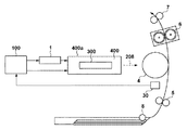
図1は、本実施形態による画像形成装置の概略的な構成図である。光走査装置400は、画像信号生成部100からの画像信号と、制御部1からの制御信号に基づき、走査光208(以下、光208と呼ぶ)を発する。光走査装置400は、光源を駆動する駆動部300を備えており、筐体400aに収容される。感光体4の表面は、不図示の帯電部により一様な電位に帯電されている。この感光体4を光208で走査・露光することで、感光体4の表面には静電潜像が形成される。不図示の現像部は、この静電潜像に現像剤を付着させ、現像剤像として可視化する。この現像剤像は、給紙ユニット8から給送され、ローラ5で感光体4と接触する位置に搬送された紙等の記録媒体に転写される。記録媒体に転写された現像剤像は、定着器6で記録媒体に熱定着され、排紙ローラ7を経て装置外に排出される。また、画像形成装置は、感光体4の表面に形成された現像剤像の濃度を検出する濃度検出センサ30(以下、センサ30と呼ぶ。)を備えている。
<First embodiment>
FIG. 1 is a schematic configuration diagram of the image forming apparatus according to the present embodiment. The
図2は、本実施形態による光走査装置400の構成図であり、図2(A)は主走査方向における断面を、図2(B)は副走査方向における断面を示している。なお、主走査方向とは、感光体4の表面において光208を走査する方向であり、副走査方向とは、感光体4の表面において主走査方向と直交する方向である。本実施形態において、光源401から出射した光(光束)208は、開口絞り402によって楕円形状に整形されてカップリングレンズ403に入射する。カップリングレンズ403を通過した光は、略平行光に変換されて、アナモフィックレンズ404に入射する。なお、略平行光とは、弱収束光及び弱発散光を含む。アナモフィックレンズ404は、主走査方向の断面内においては正の屈折力を有しており、入射する光束を主走査方向の断面内において収束光に変換する。また、アナモフィックレンズ404は、副走査方向の断面内においては、偏向器405の偏向面405aの近傍に光束を集光し主走査方向に長い線像を形成する。
2A and 2B are configuration diagrams of the
アナモフィックレンズ404を通過した光は、偏向器(回転多面鏡)405の反射面405aにて反射される。反射面405aで反射した光208は、結像レンズ406を透過し、感光体4の被走査面407に光スポットを形成する。結像レンズ406は、結像光学素子である。本実施形態においては、単一の結像光学素子(結像レンズ406)のみで結像光学系が構成されている。偏向器405を不図示の駆動部により矢印A方向に一定の角速度で回転させることにより、被走査面407上で光スポットが主走査方向に移動し、これにより感光体4を走査する。図2に示す様に、光スポットは、感光体4の被走査面407を、主走査方向において距離Wだけ走査して1走査線の各画素を露光する。感光体4の表面の感光体4の回転により副走査方向に移動し、副走査方向において複数の走査線を露光することで、被走査面407上に静電潜像が形成される。
The light that has passed through the
ビーム検出器(BD)センサ409と、BDレンズ408は、被走査面407上に静電潜像を書き込むタイミングを決定する同期用光学系である。BDレンズ408を通過した光は、フォトダイオードを含むBDセンサ409に入射し検出される。BDセンサ409により光を検知したタイミングに基づいて、書き込みタイミングの制御が行われる。
A beam detector (BD)
光源401は、例えば、半導体レーザである。本実施形態の光源401は、1つの発光部を備えている。しかしながら、独立して発光制御可能な複数の発光部を備える光源401を使用できる。複数の発光部を備える場合、生成される複数の光束は、それぞれカップリングレンズ403、アナモフィックレンズ404、偏向器405、結像レンズ406を経由して被走査面407へ到達する。被走査面407上では副走査方向にずれた位置に各光束に対応する光スポットがそれぞれ形成される。なお、上述した、光源401、カップリングレンズ403、アナモフィックレンズ404、結像レンズ406、偏向器405等の光走査装置400の各種光学部材は、図1に示す筐体400aに収納される。
The
図2に示すように、結像レンズ406は、入射面406a及び出射面406bの2つの光学面を有する。結像レンズ406は、偏向面405aにて偏向された光を、被走査面407上において所定の走査特性で走査させる。また、結像レンズ406は、被走査面407上での光スポットを所定の形状にする。また、結像レンズ406により、副走査方向の断面内においては、偏向面405aの近傍と被走査面407の近傍とで共役の関係が成立する。これにより、面倒れを補償、つまり、偏向面405aが倒れた際の被走査面407上での副走査方向の走査位置ずれを低減する構成となっている。
As shown in FIG. 2, the
なお、本実施形態よる結像レンズ406は、射出成形によって形成されたプラスチックモールドレンズであるが、結像レンズ406としてガラスモールドレンズを採用してもよい。モールドレンズは、非球面形状の成形が容易であり、かつ大量生産に適しているため、結像レンズ406としてモールドレンズを採用することで、その生産性及び光学性能の向上を図ることができる。
The
本実施形態による結像レンズ406は、所謂、fθ特性を有するものではない。つまり、偏向器405を等角速度で回転させた時に、被走査面407上で、光スポットは等速で移動しない。このように、fθ特性を有していない結像レンズ406を用いることにより、図2(A)の距離D1を短く、つまり、結像レンズ406を偏向器405に近接して配置することが可能となる。また、fθ特性を有していない結像レンズ406は、fθ特性を有する結像レンズよりも、主走査方向の長さLWと、光軸方向の厚みLTが小さくなる。よって、fθ特性を有さいない結像レンズ406により、光走査装置400の筐体400aを小型化できる。また、fθ特性を有するレンズは、主走査方向の断面において、レンズの入射面と出射面の形状に急峻な変化があるものがあり、良好な結像性能を得られない可能性がある。これに対して、fθ特性を有さいない結像レンズ406の形状は、この様な急峻な変化が少なく、よって、良好な結像性能を得ることができる。
The
本実施形態の結像レンズ406による被走査面407での走査特性は、以下の式(1)で表される。
Y=K/B・tan(B・θ) (1)
式(1)のYは、被走査面407の主走査方向における光スポットの位置(像高)であり、光スポットが光軸上(以下、単に軸上と呼ぶ。)にある場合、つまり、走査線の中心に光スポットが有る場合にY=0である。また、式(1)のθは、偏向器405による走査角度(走査画角)であり、θ=0は、光スポットが光軸上にある場合に対応する。さらに、式(1)のKは、軸上における結像係数であり、Bは、結像レンズ406の走査特性を決定する走査特性係数である。結像レンズ406により、光スポットは、Y=−Ymax〜+Ymaxの範囲を走査する。なお、図2においてYmaxはW/2である。以下、像高Yの絶対値の最大値、つまり、Y=−Ymax及びYmaxを、最大像高と呼ぶものとする。また、像高Y=0を、軸上像高と呼ぶものとする。
The scanning characteristic on the scanned
Y = K / B · tan (B · θ) (1)
Y in Expression (1) is the position (image height) of the light spot in the main scanning direction of the surface to be scanned 407, and when the light spot is on the optical axis (hereinafter simply referred to as the axis), that is, Y = 0 when there is a light spot at the center of the scanning line. Further, θ in Expression (1) is a scanning angle (scanning field angle) by the
式(1)を走査角度θで微分すると、被走査面407の主走査方向位置に対する光スポットの移動速度、つまり走査速度を示す以下の式(2)が得られる。
dY/dθ=K/(cos2(B・θ) (2)
式(2)より、θ=0のとき、つまり、軸上像高での光スポットの走査速度はKである。式(2)をKで除すると、以下の式(3)が得られる。
(dY/dθ)/K=1/(cos2(B・θ) (3)
式(3)は、軸上像高での光スポットの走査速度に対する、各走査角での光スポットの走査速度の比を表している。なお、像高と走査角は対応するため、式(3)は、軸上像高での光スポットの走査速度と、各像高での光スポットの走査速度の比を示している。式(1)から1を引いた以下の式(4)は、よって、軸上像高での光スポットの走査速度に対する、各像高での走査速度のずれ量(以下、部分倍率と呼ぶ)を示している。
(dY/dθ)/K=(1/(cos2(B・θ))−1=tan2(B・θ) (4)
式(3)及び式(4)から、本実施形態による結像レンズ406では、偏向器405の像高により光スポットの走査速度が変化することが分かる。つまり、本実施形態による光走査装置400は、走査線内において走査速度が変化する。
When the equation (1) is differentiated by the scanning angle θ, the following equation (2) indicating the moving speed of the light spot with respect to the position in the main scanning direction of the surface to be scanned 407, that is, the scanning velocity is obtained.
dY / dθ = K / (cos 2 (B · θ) (2)
From equation (2), when θ = 0, that is, the scanning speed of the light spot at the on-axis image height is K. When equation (2) is divided by K, the following equation (3) is obtained.
(DY / dθ) / K = 1 / (cos 2 (B · θ) (3)
Equation (3) represents the ratio of the scanning speed of the light spot at each scanning angle to the scanning speed of the light spot at the on-axis image height. Since the image height corresponds to the scanning angle, Expression (3) indicates the ratio of the scanning speed of the light spot at the on-axis image height to the scanning speed of the light spot at each image height. The following formula (4) obtained by subtracting 1 from the formula (1) is thus the amount of deviation of the scanning speed at each image height with respect to the scanning speed of the light spot at the on-axis image height (hereinafter referred to as partial magnification). Is shown.
(DY / dθ) / K = (1 / (cos 2 (B · θ)) − 1 = tan 2 (B · θ) (4)
From the expressions (3) and (4), it can be seen that in the
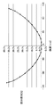
図3は、像高に対する部分倍率のグラフである。図3に示す様に、像高Yの絶対値が大きくなると、走査速度が速くなるため部分倍率が大きくなる。例えば、部分倍率が30%であると、単位時間だけ光照射した場合、被走査面407における主走査方向の照射長が、軸上の1.3倍になる。従って、画像クロックの周期によって決めた一定の時間間隔で主走査方向の画素幅を決めてしまうと、光スポットの主走査方向位置に応じて画素密度が異なることになる。さらに、光源401の発光輝度を一定とすると、走査速度の違いにより、光スポットの走査位置に応じて露光量が異なることになる。具体的には、走査速度が速くなる程、単位長さ当たりの露光量が少なくなる。したがって、良好な画質を得る為に、部分倍率の補正と、単位長さ辺りの総露光量を補正する為の輝度補正を行う必要がある。
FIG. 3 is a graph of partial magnification with respect to image height. As shown in FIG. 3, as the absolute value of the image height Y increases, the scanning speed increases, so that the partial magnification increases. For example, when the partial magnification is 30%, when light is irradiated for a unit time, the irradiation length in the main scanning direction on the surface to be scanned 407 becomes 1.3 times on the axis. Therefore, if the pixel width in the main scanning direction is determined at a constant time interval determined by the period of the image clock, the pixel density varies depending on the position of the light spot in the main scanning direction. Further, if the light emission luminance of the
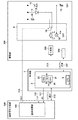
図4は、本実施形態による画像形成装置の露光制御の構成図である。画像信号生成部100は、不図示のホストコンピュータより印刷情報を受け取り、画像データ(画像信号)に対応するVDO信号110を生成する。制御部1は、画像形成装置の制御を行う。なお、制御部1は、駆動部300を制御して光源401の輝度(発光強度)の制御も行う。駆動部300は、VDO信号110に基づいて電流を光源401の発光部11に供給することにより、光源401の発光部11を発光させる。
FIG. 4 is a configuration diagram of exposure control of the image forming apparatus according to the present embodiment. The image
画像信号生成部100は、画像形成のための画像信号の出力の準備が整ったら、シリアル通信113により、制御部1に印刷開始を指示する。制御部1は、印刷の準備が整ったら、副走査方向の同期信号であるTOP信号112と、主走査方向の同期信号であるBD信号111を画像信号生成部100に送信する。画像信号生成部100は、同期信号を受信したら所定タイミングで画像信号であるVDO信号110を駆動部300に出力する。図4に示す画像信号生成部100、制御部1。駆動部300内の構成ブロックの詳細については後述する。
When the image
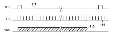
図5は、記録媒体1ページ分に相当する画像形成動作を行った際の各種同期信号と画像信号のタイミングチャートである。なお、図中左から右に向かって時間が経過する。TOP信号112の「HIGH」は、記録媒体の先端が所定の位置に到達したことを示している。画像信号生成部100は、TOP信号112の「HIGH」を受信したら、BD信号111に同期して、VDO信号110を送信する。このVDO信号110に基づいて光源401が発光し感光体4に静電潜像を形成する。なお、図5では図の簡略化の為、VDO信号110が複数のBD信号111を跨いで連続的に出力されているように記載している。しかしながら、実際には、VDO信号110は、BD信号111が出力されてから次のBD信号111が出力されるまでの間のうちの所定の期間に出力されるものである。また、BD信号111は、各走査線の開始タイミングの基準を示す信号である。
FIG. 5 is a timing chart of various synchronization signals and image signals when an image forming operation corresponding to one page of the recording medium is performed. Note that time elapses from left to right in the figure. “HIGH” in the
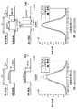
図6は、特許文献1の部分倍率補正と、輝度補正を行った場合における主走査方向の1画素(ドット)のLSFプロファイルを示している。図6(A)は軸上像高、つまり、Y=0でのLSFプロファイル、図6(B)は、最大像高、つまり、Y=YmaxでのLSFプロファイルである。さらに、図6(C)は図6(A)と図6(B)のLSFプロファイルを重ねて記載したものである。図6(A)〜(C)において、解像度は600dpiであり、1ドットの主走査方向の幅は42.3umである。なお、最大像高における部分倍率は35%である。特許文献1の構成では、軸上像高において輝度P3で時間T3だけ発光する場合、最大像高では、輝度1.35×P3で、時間0.74×T3だけ発光する。図6(C)に示す様に、軸上像高と最大像高での1ドットのLSFプロファイルを比較すると、最大像高では、軸上像高のときと比較し、積算光量のピークが低く、プロファイルの裾野部分の幅が広くなっている。つまり、LSFプロファイルは一致していない。より詳細には、像高、つまり、光スポットの主走査方向の位置によりLSFプロファイルが異なることになる。
FIG. 6 shows an LSF profile of one pixel (dot) in the main scanning direction when partial magnification correction and luminance correction of
このように、像高によりLSFプロファイルが異なるのは、図6(A)、図6(B)にそれぞれ破線で示した静止スポットのプロファイルが像高により異なるからである。なお、静止スポットのプロファイルとは、ある瞬間における光スポットのプロファイルである。つまり、1画素のLSFプロファイルは、1画素内の光スポットのプロファイルを積算したものである。 Thus, the reason why the LSF profile differs depending on the image height is that the profile of the stationary spot indicated by the broken line in FIGS. 6A and 6B differs depending on the image height. The stationary spot profile is a light spot profile at a certain moment. That is, the LSF profile of one pixel is obtained by integrating the light spot profiles in one pixel.
特許文献1に記載の構成で、像高によりLSFプロファイルが異なるのは、結像レンズ406によって被走査面407に各瞬間に生じる静止スポットの形状(プロファイル)が像高により異なるからである。よって、本実施形態では、部分倍率補正と輝度補正に加え、光源401の発光時間の補正(発光時間補正)を行う。これにより、細密画像の再現性を向上させる。
In the configuration described in
図7(A)は、特許文献1による1ドットの光波形及びLSFプロファイルを示し、図7(B)は、本実施形態による1ドットの光波形及びLSFプロファイルを示している。ここで、光波形は、1ドットの発光時間及び輝度を示し、軸上像高、中間像高及び最大像高の3つについて示している。なお、中間像高とは、軸上像高と最大像高の間における像高である。なお、図7(A)及び(B)において、軸上像高での1画素(42.3μm)の走査時間をT3とし、このときの輝度をP3としている。また、図7(A)及び(B)において、最大像高での部分倍率は35%である。よって、最大像高における1画素の走査時間は0.74T3である。特許文献1においては、部分倍率が35%であるため、最大像高における発光時間を、1画素の走査時間に等しい0.74T3としている。本実施形態では、特許文献1の様に、部分倍率に基づき発光時間を補正するのではなく、Y=0以外では、1画素の走査時間より短い時間だけ発光させている。また、Y=0以外では、部分倍率に基づき輝度を補正するのではなく、発光時間に基づき輝度を補正する。つまり、Y=0での輝度に部分倍率を乗じた、特許文献1の輝度より大きい輝度で発光させている。例えば、図7(B)において、最大像高では、1画素の走査時間0.74T3より短い0.22T3だけ発光させている。したがって、最大像高での輝度を、軸上像高での1/0.22倍、つまり、4.50P3としている。この構成により図7(B)に示す様に、主走査方向位置の違いによる1画素のLSFプロファイルの形状の差を小さくしている。この様に、本実施形態では、部分倍率補正を行いつつ、発光時間補正を行い、加えて発光時間補正を加味した輝度補正を行う。以下、詳細に説明する。
FIG. 7A shows a one-dot optical waveform and LSF profile according to
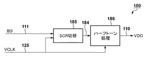
図8は、画像信号生成部100の画像変調部150の構成図である。ハーフトーン処理部186は、発光時間補正を行う。ハーフトーン処理部186は、各像高に応じたスクリーンを保持しており、SCR切替部185が出力するスクリーン切替情報184に基づき、使用するスクリーンを選択してハーフトーン処理を行う。SCR切替部185は、同期信号であるBD信号111と画像クロック信号125により、スクリーン切替情報184を生成する。図9はBD信号111と、スクリーン切替情報184との関係を示している。本実施形態では、像高の絶対値に応じて、走査線をn個の領域に分割し、各領域に対応するスクリーンをハーフトーン処理部186に保持させておく。なお、各領域を領域1〜領域nとし、軸上像高を含む領域に対応するスクリーンをSCRnとし、最大像高を含む領域に対応するスクリーンをSCR1と表記する。また、最大像高を含む領域及び軸上像高を含む領域以外の領域については、最大像高を含む領域に近い順に、SCR2〜SCRn−1のスクリーンを使用する。SCR切替部は、BD信号111のタイミングを基準とし、画像クロック信号125により現像の走査領域を判定してスクリーン切替情報184を生成する。
FIG. 8 is a configuration diagram of the
図10は、軸上像高を含む範囲で使用されるSCRnの一例であり、図11は、最大増高を含む範囲で使用されるSCR1の一例である。図10及び図11において代表して示す様に、SCRk(k=1〜n)は、200線のマトリクスとし、各画素を16分割した16の画素片で階調表現を行っている。VDO信号110の多値パラレル8ビットのデータで表された濃度情報応じて、9画素で構成されたスクリーンの面積を変化させる。マトリクス153は、階調毎に設けられており、図10及び図11の矢印で示す順に階調が上がっていく(濃度が濃くなる)。図11に示す様に、SRC1は、最も階調の高い(最大濃度)マトリクスにおいても、各画素の16区画の画素片を全点灯させないように設定している。
FIG. 10 is an example of SCRn used in the range including the on-axis image height, and FIG. 11 is an example of SCR1 used in the range including the maximum height increase. As representatively shown in FIGS. 10 and 11, SCRk (k = 1 to n) is a 200-line matrix, and gradation representation is performed by 16 pixel pieces obtained by dividing each pixel into 16 parts. In accordance with the density information represented by the multi-value parallel 8-bit data of the
一例として、図7(B)の様に、最大像高の発光時間を0.22T3と設定した場合について説明する。部分倍率補正を実行することで、1ドット(画素)に相当する走査時間は0.74T3になる。このため、最大発光時間を0.22Tに制限するには、1画素16区画分のうちの0.22/0.74に相当する区画内で発光するように設定すればよい。つまり、
16×(0.22/0.74)=4.75[区画]
となる。よって、最大5区画程度の画素片が点灯するようなスクリーンとすればよい。
As an example, a case where the light emission time at the maximum image height is set to 0.22T3 as shown in FIG. 7B will be described. By executing the partial magnification correction, the scanning time corresponding to one dot (pixel) is 0.74T3. For this reason, in order to limit the maximum light emission time to 0.22T, the light emission may be set in the section corresponding to 0.22 / 0.74 out of the 16 sections of one pixel. That means
16 × (0.22 / 0.74) = 4.75 [section]
It becomes. Therefore, a screen that illuminates pixel pieces of up to about five sections may be used.
続いて、輝度補正について説明する。既に説明した発光時間補正により、像高Yの絶対値が大きくなる程、1画素の発光時間を短くする。したがって、輝度を一定とすると、像高Yの絶対値が大きくなる程1画素への総露光量(積分した光量)が低下する。本実施形態では、この総露光量の低下を補うための輝度補正を行う。つまり、1画素への総露光量(積分光量)が各像高で一定となるように光源401の輝度を補正する。
Next, luminance correction will be described. The light emission time of one pixel is shortened as the absolute value of the image height Y is increased by the light emission time correction already described. Accordingly, if the luminance is constant, the total exposure amount (integrated light amount) for one pixel decreases as the absolute value of the image height Y increases. In the present embodiment, luminance correction is performed to compensate for the decrease in the total exposure amount. That is, the luminance of the
図4に示す様に制御部1は、CPUコア2と8ビットDAコンバータ(DAC)21とレギュレータ(REG)22を内蔵したIC3を有し、駆動部300と合わせて輝度補正部を構成している。駆動部300は、メモリ304と、電圧を電流に変換するVI変換回路306と、ドライバIC9を有し、光源401の発光部11へ駆動電流を供給する。メモリ304には、部分倍率特性情報及び発光時間特性情報と、発光部11に供給する補正電流の情報が保存されている。部分倍率特性情報は、像高に対する部分倍率を示す情報である。なお、部分倍率情報は、部分倍率そのものを示すものでなくとも良い。例えば、像高に対する走査速度を示す情報等、像高に対する部分倍率を求めることができる情報とすることができる。発光時間特性情報は、像高に対する発光時間情報である。
As shown in FIG. 4, the
制御部1のIC3は、シリアル通信307によりメモリ304から取得した、発光部11に対する補正電流の情報をもとに、レギュレータ22から出力される電圧23を調整し出力する。電圧23はDAコンバータ21の基準電圧となる。次に、IC3は、DAコンバータ21の入力データ20を設定し、BD信号111に同期して、1走査線において像高に応じて増減する輝度補正アナログ電圧312を出力する。この輝度補正アナログ電圧312は、VI変換回路306で電流値313に変換され、ドライバIC9に出力される。なお、本実施形態では、制御部1に実装されたIC3が輝度補正アナログ電圧312を出力したが、駆動部300上にDAコンバータを実装し、ドライバIC9の近傍で輝度補正アナログ電圧312を生成しても良い。
The
ドライバIC9は、VDO信号110に応じて、電流ILを発光部11に流すか、ダミー抵抗10に流すかをスイッチ14で切り替えることで、光源401の発光をON/OFF制御する。発光部11に供給する駆動電流値ILは、定電流回路15で設定した電流IaからVI変換回路306から出力される電流Idを差し引いた電流となる。発光部11の光量モニタ用に光源401に設けられたフォトディテクタ12が検出する輝度が、所定値Papc1となるように、定電流回路15に流す電流Iaは、ドライバIC9内部の回路によりフィードバック制御され自動調正される。この自動調整は、所謂APC(Automatic Power Control)である。発光部11の輝度の自動調整は、BD信号111を検出するために発光部11を発光させているタイミングで実施する。VI変換回路306が出力する電流値Idの設定方法は後述する。可変抵抗13は、工場組立て時に、発光部11が所定輝度に発光している場合に、所望の電圧としてドライバIC9に入力されるよう値を調整しておく。
The driver IC 9 performs ON / OFF control of the light emission of the
以上、所定の輝度で発光させるために必要な電流Iaに対して、VI変換回路306が出力する電流値Idを差し引いた電流を駆動電流ILとして発光部11に供給する構成としている。この構成により、駆動電流ILは電流Ia以上に流れることが無いようなっている。なお、VI変換回路306は輝度補正部の一部を構成している。
As described above, a current obtained by subtracting the current value Id output from the
図12は発光部11の電流と輝度の特性を示したグラフである。発光部11を所定輝度で発光するために必要な電流Iaは、周囲温度によって変化する。図10のグラフ51は標準温度環境下でのグラフであり、グラフ52は高温環境下でのグラフの一例である。一般的にレーザダイオード等の発光部11は、環境温度が変化した場合、所定輝度を出力させるために必要な電流Iaは変化するが、効率(図の傾き)は、ほとんど変化しないことが知られている。つまり、所定輝度Papc1で発光させるには、標準温度環境下では電流IaとしてA点で示した電流値が必要であるのに対し、高温環境下ではC点で示した電流値が必要となる。前述した通り、ドライバIC9は、環境温度が変化しても、フォトディテクタ12で輝度をモニタすることで所定輝度Papc1となるように発光部11へ供給する電流Iaを自動調整する。効率は環境温度が変化してもほぼ変化しないため、所定輝度Papc1で発光させるための電流Iaから、所定電流ΔI(N)、ΔI(H)を差し引くことで、Papc1の0.74倍の輝度に低下させることが出来る。なお、効率は環境温度が変化してもほぼ変化しないため、ΔI(N)、ΔI(H)は、ほぼ同じ値である。本実施形態は、軸上像高から最大像高に向けて発光部11の輝度を徐々に増加させるので、軸上像高では図12のB点やD点で示す輝度で発光し、最大像高A点やC点で示す輝度で発光することになる。
FIG. 12 is a graph showing the current and luminance characteristics of the
輝度補正は、所望の輝度で発光させるよう自動調整された電流Iaから像高に応じた電流ΔI(N)、ΔI(H)に対応する電流Idを差し引くことにより行う。上述したように、像高Yの絶対値が大きくなる程、走査速度が速くなる。そして、像高Yの絶対値が大きくなる程、1画素への総露光量(積分光量)が低下する。このため輝度補正では、像高Yの絶対値が大きくなる程、輝度が大きくなるように補正を行う。具体的には、像高Yの絶対値が大きくなる程、電流値Idが小さくなるように設定することで、像高Yの絶対値が大きくなる程、電流ILが大きくなるようにする。このようにして、適切に部分倍率を補正することができる。 Luminance correction is performed by subtracting current Id corresponding to image height ΔI (N) and ΔI (H) from current Ia automatically adjusted to emit light at a desired luminance. As described above, the scanning speed increases as the absolute value of the image height Y increases. As the absolute value of the image height Y increases, the total exposure amount (integrated light amount) for one pixel decreases. Therefore, in the luminance correction, the correction is performed so that the luminance increases as the absolute value of the image height Y increases. Specifically, the current value Id is set so as to decrease as the absolute value of the image height Y increases, so that the current IL increases as the absolute value of the image height Y increases. In this way, the partial magnification can be appropriately corrected.
以上、本実施形態では、感光体4の画素を露光する光スポットの走査速度は、走査線内において変化する。より詳しくは、像高の絶対値が大きくなると光スポットの走査速度は速くなる。このため、図4の露光制御構成を用いて説明した様に、露光する画素に応じて光源401の輝度及び発光時間を制御する。具体的には、画像変調部150は、発光時間を制御するためのスクリーンを保持している。また、制御部1は、メモリ304が保持する補正電流の値に関する情報を使用して光源401の輝度を制御する。このスクリーンは、画素に対する発光時間を示す情報であり、補正電流の値は、画素に対する輝度を示す情報であり、これらを纏めて走査情報と呼ぶものとする。画像形成装置は、この走査情報を使用し、露光する画素に対する光源の輝度及び発光時間を制御する。
As described above, in the present embodiment, the scanning speed of the light spot that exposes the pixels of the
なお、図7(B)を用いて説明した様に、画素の発光時間が規定されていると、当該画素の輝度は、軸上像高の画素の発光時間及び輝度から決定することができる。以下、軸上像高の画素に対する発光時間及び輝度を、それぞれ、基準発光時間及び基準輝度と呼び、軸上像高の画素を基準画素と呼ぶ。基準画素は、走査線の中央の画素でもあり、また、走査時間の最も長い画素でもある。図7(B)に示す様に、画素に対する輝度は、当該画素の発光時間と基準発光時間の比と、基準発光時間から求めることができる。画素の発光時間ではなく、輝度が規定されている場合でも、同様に、当該画素の発光時間を求めることができる。したがって、走査情報としては、露光する画素に対する光源の輝度及び発光時間のいずれかのみを含める構成であっても良い。また、図7(B)に示す様に、基準画素の発光時間は、基準画素の走査時間に等しい。これに対して、図7(B)に示す様に、基準画素とは異なる画素の発光時間は、当該画素の走査時間より短い。例えば、図7(B)において、最大像高の画素の走査時間は、0.74T3であるが、発光時間は0.22T3である。 Note that, as described with reference to FIG. 7B, when the light emission time of a pixel is specified, the luminance of the pixel can be determined from the light emission time and luminance of the pixel having the axial image height. Hereinafter, the light emission time and the luminance with respect to the pixel having the axial image height are referred to as a reference light emission time and the reference luminance, respectively, and the pixel having the axial image height is referred to as a reference pixel. The reference pixel is also the pixel at the center of the scanning line and the pixel with the longest scanning time. As shown in FIG. 7B, the luminance for the pixel can be obtained from the ratio of the light emission time of the pixel to the reference light emission time and the reference light emission time. Even when the luminance is defined instead of the light emission time of the pixel, the light emission time of the pixel can be similarly obtained. Therefore, the scanning information may include only one of the luminance of the light source and the light emission time for the pixel to be exposed. Further, as shown in FIG. 7B, the light emission time of the reference pixel is equal to the scanning time of the reference pixel. On the other hand, as shown in FIG. 7B, the light emission time of a pixel different from the reference pixel is shorter than the scanning time of the pixel. For example, in FIG. 7B, the scanning time of the pixel having the maximum image height is 0.74T3, but the light emission time is 0.22T3.
以上の通り、発光時間及び輝度を制御することで、fθ特性を有する走査レンズを用いることなく、歪を抑えた精度の良い露光を行うことができる。なお、図4に示す露光制御構成において、発光時間及び輝度の制御は、画像信号生成部100と、制御部1と、駆動部300が協働して実行していた。しかしながら、本発明はその様な形態に限定されず、例えば、1つの制御部のみにより、或いは、任意の数の機能ブロックが協働することにより発光時間及び輝度の制御を行う構成とすることができる。
As described above, by controlling the light emission time and luminance, it is possible to perform exposure with high accuracy while suppressing distortion without using a scanning lens having fθ characteristics. In the exposure control configuration shown in FIG. 4, the light emission time and the brightness are controlled by the image
以上の通り、光走査装置400単体での特性に基づく発光時間及び輝度の補正制御について説明を行った。しかしながら、光走査装置400を画像形成装置に搭載する際の組み付け位置ばらつきによって、光走査装置400と被走査面である感光体4との位置関係が理想的な関係からズレることが生じ得る。その結果、感光体4の表面での走査特性が変動する。この様な場合、光走査装置400単体の特性に基づき、上述した補正を行ったとしても、光スポットのプロファイルを適切に補正することができなくなる。
As described above, the light emission time and luminance correction control based on the characteristics of the
図13は、スポットのプロファイルが主走査方向で不均一な状態において形成されたハーフトーン画像の濃度測定値の一例を示すグラフである。図13(A)は、濃度20%に対応する画像データでハーフトーン画像を形成した場合の特性であり、像高の絶対値が大きくなると濃度が薄くなっている。一方、図13(B)は、濃度80%に対応する画像データでハーフトーン画像を形成した場合の特性であり、像高の絶対値が大きくなると濃度が濃くなっている。このように、光スポットのプロファイルが適切に補正できないと、像高の絶対値が大きくなるにつれ濃度変動が大きくなり得る。したがって、光走査装置400を画像形成装置に搭載する際の位置ばらつきに対し、位置ズレ分を補正する必要がある。本実施形態では、センサ30を用いて光スポットのプロファイルを適切に補正する。
FIG. 13 is a graph showing an example of density measurement values of a halftone image formed in a state where the spot profile is non-uniform in the main scanning direction. FIG. 13A shows characteristics when a halftone image is formed with image data corresponding to a density of 20%. The density decreases as the absolute value of the image height increases. On the other hand, FIG. 13B shows characteristics when a halftone image is formed with image data corresponding to a density of 80%, and the density increases as the absolute value of the image height increases. Thus, if the profile of the light spot cannot be corrected appropriately, the density variation can increase as the absolute value of the image height increases. Therefore, it is necessary to correct the positional deviation with respect to the positional variation when the
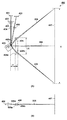
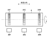
図14は、本実施形態による濃度検出の説明図である。感光体4の主走査方向に沿って3つのセンサ30F、30C、30Rを配置している。センサ30は、発光ダイオード(LED)のような発光素子と、受光素子とを備えた正反射型のセンサである。センサ30は、感光体4に形成した濃度検出用の現像剤像であるパッチ31に対し発光素子から光を照射し、反射光を受光素子により受光する。このとき、パッチ31のトナー部に反射した光は散乱光となるため、受光素子が受光する反射光は、大半が感光体4の表面で正反射した光である。したがって、センサ30が受光する光量から、パッチ31の濃度を測定することができる。
FIG. 14 is an explanatory diagram of density detection according to the present embodiment. Three
また、本実施形態においては、センサ30Cを軸上像高に配置し、センサ30F及び30Rを最大像高付近に配置している。これは、軸上像高の走査速度が安定しており、光走査装置400の位置が多少ズレたとしても、光スポットのプロファイルがズレにくいためである。つまり、軸上像高では濃度変動が発生し難いので、センサ30Cの測定値を基準として、濃度変動が発生しやすい最大像高付近における濃度変動をセンサ30F及び30Rを用いて測定することができる。
In the present embodiment, the
なお、本実施形態ではセンサ30の数を3個としたが、本発明はこれに限定されない。例えば、3個以上のセンサ30を配置すれば、主走査方向全域に渡る濃度変動をより正確に検出することができる。また、走査速度のプロファイルは基本的に対称性があるため、最大像高付近のセンサを1つとすることもできる。例えば、センサ30C及びセンサ30Fの2つを設ける構成であっても良い。また、本実施形態では感光体4上に形成したパッチを測定する構成であるが、中間転写体(不図示)を搭載した画像形成装置の場合は、感光体4から中間転写体に転写されたパッチを測定する構成でも良い。パッチ31F、31C及び31Rは、各センサ30に対応するように形成する。また、各パッチ31は、それぞれ、低濃度から高濃度までの連続した階調のパッチとする。
In the present embodiment, the number of
図15は、センサ30によるパッチ31の検出結果を示す一例である。なお、グラフ32はセンサ30Cの検出結果であり、グラフ33はセンサ30Fの検出結果であり、グラフ34はセンサ30Rの検出結果である。図13の像高と濃度の関係から明らかなように、センサ30Cのグラフ32に比べ、センサ30F及びセンサ30Rのグラフ33及びグラフ34の方が急峻な階調濃度特性を示す。
FIG. 15 is an example showing a detection result of the patch 31 by the
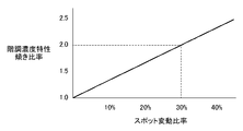
次に、光スポットのプロファイルを補正する方法について説明する。図1に示す様に、センサ30は、画像信号生成部100に接続されている。画像信号生成部100は、センサ30Cで測定した階調濃度特性を基準として取得し、センサ30F及び30Rで測定した階調濃度特性とを比較することにより、光スポットのプロファイルの変動を求める。本実施形態では、図15に示すように、濃度30%から70%の区間での階調濃度特性の傾きを用いる。画像信号生成部100は、センサ30Cで測定した傾きを基準値として、センサ30F及び30Rで測定した傾きの基準値の比率を算出する。また、駆動部300のメモリ304は、算出した比率と、光スポットの変動比率とを関連付ける不図示のテーブルを保存している。画像信号生成部100は、算出した比率に対応する光スポットの変動比率に基づき、上述した様に決定した発光時間及び輝度の両方、又は、いずれか一方を補正する。なお、算出した比率から光スポットの変動比率を求める方法としては、テーブルの代わりに、算出した比率とスポットの変動比率とを関連付ける計算式を用いても良い。図16は、算出した階調濃度特性の傾きの比率と、光スポットの変動比率との関係例を示している。なお、図16にその例を示す関係は、光走査装置400の特性や画像形成装置の構成によって変わるため、画像形成装置ごとに固有のテーブルまたは計算式を予め求めておく。また、光スポットの変動比率と、発光時間や輝度の補正値の関係も、予め求めてメモリ304に保存しておく。なお、光スポットの変動比率と、発光時間や輝度の補正値の関係は、テーブルとして保存する形態であっても、計算式として保存する形態であっても良い。
Next, a method of correcting the light spot profile will be described. As shown in FIG. 1, the
なお、本実施形態では、濃度検出のためのパッチとして低濃度から高濃度までの複数階調のパッチを形成していたが、本発明はこの構成に限定されない。具体的には、像高に応じた濃度変動を検知できるパターンであればよい。例えば濃度30%と濃度70%に対応する画像データで形成した2種類のパッチの検出濃度から傾きを求めてもよい。さらに、階調濃度特性の傾きの比率により、光スポットの変動比率を求めたが、本発明はこの構成に限定されない。つまり、光スポットの変動と相関のあるパラメータであれば良く、例えば、特定の画像データのパッチの検出濃度を比較する構成でも、比率ではなく差を使用する構成であっても良い。 In the present embodiment, patches of multiple gradations from low density to high density are formed as patches for density detection, but the present invention is not limited to this configuration. Specifically, any pattern that can detect density fluctuations according to the image height may be used. For example, the slope may be obtained from the detected densities of two types of patches formed with image data corresponding to a density of 30% and a density of 70%. Furthermore, the variation ratio of the light spot is obtained from the gradient ratio of the gradation density characteristics, but the present invention is not limited to this configuration. That is, any parameter that correlates with fluctuations in the light spot may be used. For example, a configuration that compares the detected densities of patches of specific image data or a configuration that uses a difference instead of a ratio may be used.
以上、本実施形態では、光スポットの走査位置、つまり露光する画素の位置による変化を示すプロファイル情報を保持しておく。プロファイル情報とは、例えば、上述した、画素の位置による光スポットの変動比率である。そして、画像形成装置は、画素に対する光源の輝度及び発光時間を決定するに当たり、上述した走査情報及びプロファイル情報を使用する。例えば、走査情報に基づき決定した画素に対する光源の輝度及び発光時間の両方、或いは、いずれか一方を、プロファイル情報に基づき補正する。なお、制御部1は、感光体4に濃度を検出するパッチ31を形成し、これにより、主走査方向における各画素での濃度の変化を検出してプロファイル情報を生成する。具体的には、主走査方向の複数の位置にセンサ31F、31C、31Rを設け、各センサで検出した濃度に基づき、主走査方向における各画素での濃度の変化を検出する。なお、センサの位置は、例えば、少なくとも走査線の中央と、端部に設ける構成とすることができる。この構成により、像高の変化による濃度変動に拘らず、光スポットのプロファイルを補正することができる。その結果、fθ特性を有する走査レンズを用いることなく、歪を抑えた精度の良い露光を行うことが可能となる。
As described above, in the present embodiment, the profile information indicating the change depending on the scanning position of the light spot, that is, the position of the pixel to be exposed is held. The profile information is, for example, the above-described light spot variation ratio depending on the pixel position. Then, the image forming apparatus uses the above-described scanning information and profile information in determining the luminance of the light source and the light emission time for the pixel. For example, the luminance and / or the light emission time of the light source for the pixel determined based on the scanning information are corrected based on the profile information. Note that the
<第二実施形態>
続いて、第二実施形態について第一実施形態との相違点を中心に説明する。第一実施形態では、光走査装置400の位置ばらつきによる光スポットの変動に対して、濃度測定結果から光スポットの変動比率を求め、発光時間および輝度を補正していた。本実施形態では、光走査装置400を画像形成装置に組み付けた後、光スポットを直接測定する。光スポットを測定する方法は、例えば、一般的な計測器のスポット測定機能を使用すればよい。この方法では測定作業が発生するため、第一実施形態の構成に比べコストアップするものの、スポットを直接測定できるため、より高精度にスポットを補正することができる。本実施形態ではスポット情報検出部として計測器500を使用する。
<Second embodiment>
Next, the second embodiment will be described focusing on the differences from the first embodiment. In the first embodiment, the variation ratio of the light spot is obtained from the density measurement result with respect to the variation of the light spot due to the positional variation of the
図17は、本実施形態による光スポットの測定構成を示している。光スポットを測定する為の計測器500は、図1の感光体4を取り外した状態で設置し、光208の光スポットのプロファイルを測定する。この時、計測器500の受光面は、感光体4の受光面と一致するように配置することで、感光体4の表面上での光スポットのプロファイルを測定することができる。
FIG. 17 shows a measurement configuration of a light spot according to the present embodiment. A measuring
次に、光スポットのプロファイルの補正方法について説明する。計測器500によって測定した光スポットのプロファイル情報は、駆動部300のメモリ304に書き込まれる。また、メモリ304には、光スポットの基準値を保持させる。画像信号生成部100は、メモリ304に保存された光スポットのプロファイルの基準値から、増高に対する光スポットの変動比率を算出し、算出した光スポットの変動比率に基づき、発光時間および輝度の補正値を更新する。なお、発光時間および輝度の補正方法は、第一実施形態と同様であり、その説明については省略する。また、計測器500はスポットの測定後取り外し、感光体4を装着する。
Next, a light spot profile correction method will be described. The light spot profile information measured by the measuring
なお、感光体4が着脱できない構成の画像形成装置であれば、例えば、光走査装置400と感光体4との間に計測器500を配置して光スポットのプロファイルを測定することもできる。この構成を用いる場合は、計測器500の受光面と感光体4の受光面が一致しないものの、互いの位置関係とレンズの光学特性に基づき、測定した光スポットから、感光体4の表面に生じる光スポットを求めることができる。
Note that if the image forming apparatus has a configuration in which the
以上説明したように、本実施形態によれば、光走査装置400を画像形成装置に組み付けた後に、光スポットのプロファイルを直接測定することにより、光走査装置400の位置ばらつきがある場合でも適切に光スポットのプロファイルを補正することができる。その結果、fθ特性を有する走査レンズを用いることなく、歪を抑えた精度の良い露光を行うことが可能となる。
As described above, according to the present embodiment, after the
<第三実施形態>
続いて、第三実施形態について第一実施形態及び第二実施形態との相違点を中心に説明する。第一実施形態及び第二実施形態では、光走査装置400の組み付け位置のばらつきに対する光スポットの補正を行っていた。しかし、光スポットの変動要因は組み付け位置のばらつき以外の要因でも生じる。例えば、画像形成装置の内部温度が連続印刷等の影響で上昇し、結像レンズ406等が熱膨張して結像特性が変化することにより、光スポットのプロファイルが変動することがある。本実施形態では、この様な、画像形成装置の環境の変化による光スポットのプロファイル変動も補正する。本実施形態では、この環境を示す情報として温度を用い、よって、画像形成装置の内部の温度を測定する温度検出部として温度センサ550を設ける。
<Third embodiment>
Next, the third embodiment will be described with a focus on differences from the first embodiment and the second embodiment. In the first embodiment and the second embodiment, the light spot is corrected with respect to variations in the assembly position of the
図18は、本実施形態による画像形成装置の構成図である。第一実施形態及び第二実施形態と異なる点は、光走査装置400の周辺に温度センサ550を配置している点である。また、光走査装置400の位置ばらつきによる影響は、第二実施形態による方法により補正を行う。しかしながら、第一実施形態と同様に、センサ300を配置して補正する形態であっても良い。
FIG. 18 is a configuration diagram of the image forming apparatus according to the present embodiment. The difference from the first embodiment and the second embodiment is that a
温度センサ550は、画像信号生成部100に接続され、測定した温度情報を画像信号生成部100に送信する。駆動部300のメモリ304は、温度センサ550により測定した温度情報と、感光体4上の光スポットのプロファイルとの関係を示す、不図示のテーブルを保存している。結像レンズ406の熱膨張と結像特性には相関があるので、光走査装置400の周辺温度と光スポットのプロファイルとの相関を取ることで、上記テーブルを作成することが可能である。また、メモリ304は、光スポットの基準値を保存している。
The
次に、光スポットのプロファイルの補正方法について説明する。画像信号生成部100は、温度センサ550により測定した温度情報から、テーブルに基づいて光スポットのプロファイルを求める。さらに、メモリ304に保存された基準値から、スポットの変動比率を算出する。算出したスポットの変動比率に基づき、発光時間および輝度の補正値を更新することで、スポットのプロファイルを適切に補正することができる。発光時間および輝度の補正方法については、第一実施形態と同様であり、その説明は省略する。
Next, a light spot profile correction method will be described. The image
以上説明したように、本実施形態によれば、光走査装置400の位置ばらつきに加え、画像形成装置が設置された環境の変化や、動作状態の変化による影響も含めた機械的な影響による光スポットのプロファイル変動を補正することが可能である。その結果、fθ特性を有する走査レンズを用いることなく、歪を抑えた精度の良い露光を行うことが可能となる。
As described above, according to the present embodiment, in addition to the positional variation of the
[その他の実施形態]
本発明は、上述の実施形態の1以上の機能を実現するプログラムを、ネットワーク又は記憶媒体を介してシステム又は装置に供給し、そのシステム又は装置のコンピュータにおける1つ以上のプロセッサーがプログラムを読出し実行する処理でも実現可能である。また、1以上の機能を実現する回路(例えば、ASIC)によっても実現可能である。
[Other Embodiments]
The present invention supplies a program that realizes one or more functions of the above-described embodiments to a system or apparatus via a network or a storage medium, and one or more processors in a computer of the system or apparatus read and execute the program This process can be realized. It can also be realized by a circuit (for example, ASIC) that realizes one or more functions.
4:感光体、400:光走査装置、1:制御部、304:メモリ 4: Photoconductor, 400: Optical scanning device, 1: Control unit, 304: Memory
Claims (14)
光源が発する光により前記感光体に光スポットを形成し、当該光スポットを走査することで走査線の各画素を露光して前記感光体に潜像を形成する走査手段であって、前記感光体を前記光スポットで走査する走査速度は、前記走査線内において変化する走査手段と、
露光する画素に応じて、前記光源の輝度及び発光時間を補正制御する制御手段と、
前記光スポットの環境による変化、或いは、前記光スポットの前記画素の位置による変化を示すプロファイル情報を保持する保持手段と、
を備えており、
前記制御手段は、前記補正制御に、前記プロファイル情報を使用することを特徴とする画像形成装置。 A photoreceptor,
Scanning means for forming a light spot on the photosensitive member by light emitted from a light source and exposing each pixel of a scanning line by scanning the light spot to form a latent image on the photosensitive member. A scanning speed at which the light spot is scanned with a scanning means that changes within the scanning line;
Control means for correcting and controlling the luminance and light emission time of the light source according to the pixel to be exposed;
Holding means for holding profile information indicating a change due to the environment of the light spot or a change due to the position of the pixel of the light spot;
With
The image forming apparatus, wherein the control unit uses the profile information for the correction control.
前記制御手段は、前記走査情報及び前記プロファイル情報に基づき前記補正制御を行うことを特徴とする請求項1に記載の画像形成装置。 The holding unit holds scanning information indicating a light emission time of the light source or a luminance of the light source with respect to a pixel for correcting a change in the scanning time of the pixel due to a change in the scanning speed;
The image forming apparatus according to claim 1, wherein the control unit performs the correction control based on the scanning information and the profile information.
前記制御手段は、画素に対する前記光源の発光時間が短くなると、当該画素に対する前記光源の輝度が高くなる様に、画素に対する前記光源の輝度を決定し、前記プロファイル情報に基づき当該画素に対する前記光源の発光時間及び前記決定した輝度のいずれか、又は、両方を補正することを特徴とする請求項2に記載の画像形成装置。 The scanning information indicates a light emission time of the light source with respect to a pixel,
The control means determines the luminance of the light source for the pixel so that the luminance of the light source for the pixel increases when the light emission time of the light source for the pixel becomes short, and based on the profile information, determines the luminance of the light source for the pixel. The image forming apparatus according to claim 2, wherein either or both of a light emission time and the determined luminance are corrected.
前記制御手段は、画素に対する前記光源の輝度が高くなると、当該画素に対する前記光源の発光時間が短くなる様に、画素に対する前記光源の発光時間を決定し、前記プロファイル情報に基づき当該画素に対する前記光源の輝度及び前記決定した発光時間のいずれか、又は、両方を補正することを特徴とする請求項2に記載の画像形成装置。 The scanning information indicates a luminance of the light source with respect to a pixel,
The control means determines the light emission time of the light source for the pixel so that the light emission time of the light source for the pixel becomes shorter when the luminance of the light source for the pixel becomes higher, and the light source for the pixel based on the profile information 3. The image forming apparatus according to claim 2, wherein one or both of the luminance of light and the determined light emission time are corrected.
画素に対する前記光源の発光時間は、当該画素に対して使用するスクリーンにより示されることを特徴とする請求項2に記載の画像形成装置。 The scanning information indicates a light emission time of the light source with respect to a pixel,
The image forming apparatus according to claim 2, wherein a light emission time of the light source for a pixel is indicated by a screen used for the pixel.
前記感光体に形成された現像剤像の濃度を検出する濃度検出手段と、
をさらに備えており
前記制御手段は、前記感光体の走査位置による前記現像剤像の濃度の変化を検出して前記プロファイル情報を生成することを特徴とする請求項1から10のいずれか1項に記載の画像形成装置。 Developing means for developing a latent image formed on the photoreceptor to form a developer image;
Density detecting means for detecting the density of the developer image formed on the photoreceptor;
The profile information is generated by detecting a change in density of the developer image according to a scanning position of the photoconductor. The image forming apparatus described in 1.
前記制御手段は、前記複数の位置それぞれで検出した現像剤像の濃度に基づき、前記感光体の走査位置による濃度の変化を検出することを特徴とする請求項11に記載の画像形成装置。 The density detecting means detects the density at a plurality of positions along the scanning direction of the photoconductor by the scanning means;
The image forming apparatus according to claim 11, wherein the control unit detects a change in density depending on a scanning position of the photoconductor based on a density of a developer image detected at each of the plurality of positions.
前記制御手段は、前記温度検出手段が検出した温度に基づき前記プロファイル情報を生成することを特徴とする請求項1から13のいずれか1項に記載の画像形成装置。 A temperature detecting means for detecting the temperature of the image forming apparatus;
The image forming apparatus according to claim 1, wherein the control unit generates the profile information based on a temperature detected by the temperature detection unit.
Priority Applications (2)
| Application Number | Priority Date | Filing Date | Title |
|---|---|---|---|
| JP2015031055A JP2016150581A (en) | 2015-02-19 | 2015-02-19 | Image formation device |
| US15/040,448 US9658562B2 (en) | 2015-02-19 | 2016-02-10 | Image forming apparatus and optical scanning apparatus for scanning photosensitive member with light spot |
Applications Claiming Priority (1)
| Application Number | Priority Date | Filing Date | Title |
|---|---|---|---|
| JP2015031055A JP2016150581A (en) | 2015-02-19 | 2015-02-19 | Image formation device |
Publications (2)
| Publication Number | Publication Date |
|---|---|
| JP2016150581A true JP2016150581A (en) | 2016-08-22 |
| JP2016150581A5 JP2016150581A5 (en) | 2018-03-22 |
Family
ID=56696111
Family Applications (1)
| Application Number | Title | Priority Date | Filing Date |
|---|---|---|---|
| JP2015031055A Pending JP2016150581A (en) | 2015-02-19 | 2015-02-19 | Image formation device |
Country Status (1)
| Country | Link |
|---|---|
| JP (1) | JP2016150581A (en) |
Citations (9)
| Publication number | Priority date | Publication date | Assignee | Title |
|---|---|---|---|---|
| JPH07137338A (en) * | 1993-11-15 | 1995-05-30 | Victor Co Of Japan Ltd | Light emitting element array-using device |
| JP2003341138A (en) * | 2002-05-30 | 2003-12-03 | Ricoh Co Ltd | Light source adjuster for imaging apparatus and light source adjustment method |
| US20040190099A1 (en) * | 2003-03-31 | 2004-09-30 | Toshiba Tec Kabushiki Kaisha | Light scanning unit for use in image forming apparatus |
| JP2006171319A (en) * | 2004-12-15 | 2006-06-29 | Samsung Yokohama Research Institute Co Ltd | Scanning exposure apparatus |
| JP2007182031A (en) * | 2006-01-10 | 2007-07-19 | Kyocera Mita Corp | Image-forming apparatus |
| JP2008094005A (en) * | 2006-10-13 | 2008-04-24 | Seiko Epson Corp | Optical scanner, its controlling method, and apparatus and method for forming image by using the same |
| JP2009294382A (en) * | 2008-06-04 | 2009-12-17 | Canon Inc | Image forming apparatus, its control method and control program |
| JP2010078857A (en) * | 2008-09-25 | 2010-04-08 | Canon Inc | Scanning optical apparatus, image forming apparatus and control method |
| JP2014094476A (en) * | 2012-11-08 | 2014-05-22 | Konica Minolta Inc | Image formation device |
-
2015
- 2015-02-19 JP JP2015031055A patent/JP2016150581A/en active Pending
Patent Citations (9)
| Publication number | Priority date | Publication date | Assignee | Title |
|---|---|---|---|---|
| JPH07137338A (en) * | 1993-11-15 | 1995-05-30 | Victor Co Of Japan Ltd | Light emitting element array-using device |
| JP2003341138A (en) * | 2002-05-30 | 2003-12-03 | Ricoh Co Ltd | Light source adjuster for imaging apparatus and light source adjustment method |
| US20040190099A1 (en) * | 2003-03-31 | 2004-09-30 | Toshiba Tec Kabushiki Kaisha | Light scanning unit for use in image forming apparatus |
| JP2006171319A (en) * | 2004-12-15 | 2006-06-29 | Samsung Yokohama Research Institute Co Ltd | Scanning exposure apparatus |
| JP2007182031A (en) * | 2006-01-10 | 2007-07-19 | Kyocera Mita Corp | Image-forming apparatus |
| JP2008094005A (en) * | 2006-10-13 | 2008-04-24 | Seiko Epson Corp | Optical scanner, its controlling method, and apparatus and method for forming image by using the same |
| JP2009294382A (en) * | 2008-06-04 | 2009-12-17 | Canon Inc | Image forming apparatus, its control method and control program |
| JP2010078857A (en) * | 2008-09-25 | 2010-04-08 | Canon Inc | Scanning optical apparatus, image forming apparatus and control method |
| JP2014094476A (en) * | 2012-11-08 | 2014-05-22 | Konica Minolta Inc | Image formation device |
Similar Documents
| Publication | Publication Date | Title |
|---|---|---|
| US9658562B2 (en) | Image forming apparatus and optical scanning apparatus for scanning photosensitive member with light spot | |
| KR101890016B1 (en) | Image-forming apparatus | |
| US7719559B2 (en) | Image forming apparatus, optical scanning apparatus, and auto light power control method | |
| US7515167B2 (en) | Multi-beam scanning device and image forming apparatus using the scanning device | |
| US20110199657A1 (en) | Laser driving device, optical scanning device, image forming apparatus, and laser driving method | |
| US7852363B2 (en) | Light scanning apparatus, image forming apparatus, and light power control method | |
| JP2004109658A (en) | Optical scanner and optical path adjusting method, and image forming apparatus | |
| US20180152586A1 (en) | Image forming apparatus | |
| US8953009B2 (en) | Electrophotographic image forming apparatus and image forming method | |
| JP6478693B2 (en) | Image forming apparatus | |
| JP2016150581A (en) | Image formation device | |
| US9927735B2 (en) | Image forming apparatus that divides one pixel into plurality of pixel pieces and performs exposure on pixel piece-by-pixel piece basis | |
| JP2010117556A (en) | Method of adjusting optical scanning apparatus, and optical scanning apparatus adjusted by the method | |
| JP4643159B2 (en) | Optical path adjustment method | |
| JP2005053000A (en) | Image formation device | |
| JP2006259601A (en) | Optical scanner and image forming apparatus | |
| JP2004341171A (en) | Image forming apparatus | |
| US10479108B2 (en) | Image forming apparatus | |
| JP2022056082A (en) | Image formation apparatus | |
| JP2008039914A (en) | Exposure device | |
| JP2017094637A (en) | Image formation device and control method thereof | |
| JP2007168309A (en) | Optical scanning device | |
| JP2009145398A (en) | Optical scanner, light intensity controller, image forming apparatus, and light intensity control method | |
| JP2017200750A (en) | Image forming device | |
| JP2017223733A (en) | Information processing apparatus, image forming apparatus, image processing method, and program |
Legal Events
| Date | Code | Title | Description |
|---|---|---|---|
| A521 | Request for written amendment filed |
Free format text: JAPANESE INTERMEDIATE CODE: A523 Effective date: 20180205 |
|
| A621 | Written request for application examination |
Free format text: JAPANESE INTERMEDIATE CODE: A621 Effective date: 20180205 |
|
| A131 | Notification of reasons for refusal |
Free format text: JAPANESE INTERMEDIATE CODE: A131 Effective date: 20181012 |
|
| A977 | Report on retrieval |
Free format text: JAPANESE INTERMEDIATE CODE: A971007 Effective date: 20181010 |
|
| A521 | Request for written amendment filed |
Free format text: JAPANESE INTERMEDIATE CODE: A523 Effective date: 20181210 |
|
| A02 | Decision of refusal |
Free format text: JAPANESE INTERMEDIATE CODE: A02 Effective date: 20190107 |