JP2016106902A - Endoscope apparatus - Google Patents
Endoscope apparatus Download PDFInfo
- Publication number
- JP2016106902A JP2016106902A JP2014248315A JP2014248315A JP2016106902A JP 2016106902 A JP2016106902 A JP 2016106902A JP 2014248315 A JP2014248315 A JP 2014248315A JP 2014248315 A JP2014248315 A JP 2014248315A JP 2016106902 A JP2016106902 A JP 2016106902A
- Authority
- JP
- Japan
- Prior art keywords
- data
- synchronization
- bit
- serial
- signal
- Prior art date
- Legal status (The legal status is an assumption and is not a legal conclusion. Google has not performed a legal analysis and makes no representation as to the accuracy of the status listed.)
- Pending
Links
Images
Landscapes
- Endoscopes (AREA)
- Closed-Circuit Television Systems (AREA)
- Studio Devices (AREA)
- Instruments For Viewing The Inside Of Hollow Bodies (AREA)
Abstract
Description
本発明は、スコープ(内視鏡)によって器官内壁などの被写体を観察、処置等する内視鏡装置に関し、特に、スコープ先端部に設けられた撮像素子から読み出される画素信号のシリアル伝送に関する。 The present invention relates to an endoscope apparatus that observes and treats a subject such as an inner wall of an organ with a scope (endoscope), and more particularly to serial transmission of pixel signals read from an image sensor provided at the distal end of the scope.
電子内視鏡装置においては、撮像素子がビデオスコープ先端部に設けられており、撮像素子から読み出されたアナログ画像信号は、ビデオスコープ内部に配線された信号線によってスコープ基端側/プロセッサ側へ伝送される。そして、スコープコネクタ部あるいはプロセッサ内部に設けられた画像処理回路においてデジタル化され、画像信号が生成される。 In an electronic endoscope apparatus, an image sensor is provided at the distal end portion of a video scope, and an analog image signal read from the image sensor is sent to the base end side of the scope / processor side by a signal line wired inside the video scope. Is transmitted to. Then, it is digitized in an image processing circuit provided in the scope connector unit or the processor, and an image signal is generated.
CCDを使用する場合、アナログ画素信号をスコープ先端部からプロセッサ側へ伝送する。このとき、信号線が比較的長いために信号減衰や外乱ノイズの影響により、観察画像の画質を低下させる。一方、CMOSを使用する場合、撮像素子に信号処理回路を内蔵できるため、スコープ先端部において画素信号をデジタル化し、パラレル/シリアル変換してからシリアル画素データをプロセッサ側へシリアル伝送することが容易に可能である(特許文献1参照)。 When the CCD is used, an analog pixel signal is transmitted from the distal end portion of the scope to the processor side. At this time, since the signal line is relatively long, the image quality of the observation image is lowered due to the influence of signal attenuation and disturbance noise. On the other hand, when a CMOS is used, a signal processing circuit can be built in the image sensor, so that it is easy to digitize the pixel signal at the distal end of the scope, perform parallel / serial conversion, and serially transmit serial pixel data to the processor side. It is possible (see Patent Document 1).
シリアル伝送としては、8b/10bと呼ばれる変調方式を用いたシリアル伝送方式が一般的に採用される。8b/10b変調を用いることによって、変調されたシリアル信号にクロックを埋め込む事ができる。具体的には、撮像素子から読み出される画像データをパラレル/シリアル変換部においてシリアルデータに変換し、さらに、8b/10bのデータ変換表に基づき、8ビット毎に10ビットに変換したシリアル信号を出力する。 As serial transmission, a serial transmission system using a modulation system called 8b / 10b is generally employed. By using 8b / 10b modulation, a clock can be embedded in the modulated serial signal. Specifically, the image data read from the image sensor is converted into serial data by the parallel / serial conversion unit, and further, a serial signal converted into 10 bits every 8 bits is output based on the 8b / 10b data conversion table. To do.
受信側では、送られてきた8b/10bによる変調シリアル信号から、特定のクロック・データ・リカバリ(CDR)手法を用いてRefクロックを抽出(再生)する。さらに、CDRにより再生されたRefクロックによってシリアル信号をリタイミングすることにより、8b/10b変調状態の画素データを生成する。そして、リタイミングしたシリアル信号を10ビット毎に10b/8b逆変換し、その後、シリアル/パラレル変換部によってシリアルデータをパラレルデータに変換することにより、元の画像信号を生成する。 On the receiving side, a Ref clock is extracted (reproduced) from the transmitted 8b / 10b modulated serial signal using a specific clock data recovery (CDR) technique. Further, the pixel data in the 8b / 10b modulation state is generated by retiming the serial signal with the Ref clock reproduced by the CDR. The retimed serial signal is inversely converted by 10b / 8b every 10 bits, and then serial data is converted into parallel data by a serial / parallel converter, thereby generating an original image signal.
8b/10b伝送方式のような高速シリアル伝送方式の場合、送信側、受信側にデータ量の大きい変換テーブルをもつデータ変換処理回路を設ける必要がある。このような専用回路を内視鏡システムのスコープ先端部に設けることは、スコープ先端部をできる限り細径化することへの障害となる。また、変換処理回路を撮像素子傍に設けることで、画素信号を撮像素子から読み出すとき、ノイズを発生させる恐れがある。 In the case of a high-speed serial transmission system such as the 8b / 10b transmission system, it is necessary to provide a data conversion processing circuit having a conversion table with a large amount of data on the transmission side and the reception side. Providing such a dedicated circuit at the distal end of the scope of the endoscope system is an obstacle to reducing the diameter of the distal end of the scope as much as possible. Further, by providing the conversion processing circuit near the image sensor, noise may be generated when the pixel signal is read from the image sensor.
そこで、画素データをパラレル/シリアル変換する際、決まったデータ単位(例えばパラレル信号が10bitであれば10bit)に対してその前後にスタートビット(S)、エンドビット(E)を付けた基本単位であるワード(例えば12bit)を生成し、生成したワードを繋げてシリアル化する方法が知られている(特許文献2、3参照)。
Therefore, when parallel / serial conversion of pixel data is performed, it is a basic unit in which a start bit (S) and end bit (E) are added before and after a predetermined data unit (for example, 10 bits if the parallel signal is 10 bits). A method of generating a certain word (for example, 12 bits) and serializing the generated word by connecting them is known (see
そこでは、8b/10b変調のようにクロックの埋め込みを行う代わりに、Refクロック抽出(再生)のため、周期一定のスタートビット/エンドビット(S/E)の遷移エッジを利用してRefクロックを抽出する。Refクロック抽出にはスタートビット/エンドビット(S/E)遷移周期と同じ周期、位相のイニシャルパターン信号をスコープ先端部側から送信する。 In this case, instead of embedding a clock as in 8b / 10b modulation, a Ref clock is generated by using a transition edge of a constant start bit / end bit (S / E) for Ref clock extraction (reproduction). Extract. For Ref clock extraction, an initial pattern signal having the same cycle and phase as the start bit / end bit (S / E) transition cycle is transmitted from the scope tip side.
受信(プロセッサ、またはスコープ基部)側では、スコープ起動時、先端側から送られてくるイニシャルパターンに同期クロックを同期させ、Refクロックを生成する。同期完了に従って先端部へ同期完了信号を送ると、スコープ先端部は、イニシャルパターンからシリアル映像信号に送信する信号を切り替える。イニシャルパターンとシリアル映像信号のS/Eの遷移エッジの位相は一致していることから、イニシャルパターンから生成した同期クロックによって画素データ(映像データ)が抽出され、パラレル/シリアル変換される。 On the reception (processor or scope base) side, when the scope is activated, the synchronization clock is synchronized with the initial pattern sent from the distal end side to generate the Ref clock. When a synchronization completion signal is sent to the distal end in accordance with the completion of synchronization, the scope distal end switches a signal to be transmitted from the initial pattern to the serial video signal. Since the phase of the S / E transition edge of the serial pattern coincides with the initial pattern, pixel data (video data) is extracted by the synchronous clock generated from the initial pattern, and is subjected to parallel / serial conversion.
特許文献2、3に記載された画素データの転送方法では、イニシャルパターンの送信が必須となり、イニシャルデータから映像用画素データの切り替えのためにも、スコープ先端部送信側と受信側との間で相互通信する必要がある。また、ノイズなど外乱によって信号が乱れ同期が外れた場合、イニシャルパターンに切り替えて再同期させる必要がある。しかしながら、イニシャルパターンに切り替えると、画像データをスコープ先端部からの画像データ送信が中断させることになる。このような事態が内視鏡術中に発生し、再同期、画像表示復元に時間が掛かると、内視鏡作業に悪影響を与える。特に、ワード単位の同期クロックを再生するのには時間がかかってしまう。
In the pixel data transfer methods described in
したがって、簡素な回路構成によって、同期ずれなく安定して画素データをスコープ先端部からプロセッサ側へ高速にシリアル伝送し、また同期ずれが生じても速やかに再同期できることが求められる。 Accordingly, it is required that pixel data is stably serially transmitted from the distal end portion of the scope to the processor side at high speed with a simple circuit configuration, and can be quickly resynchronized even if synchronization is lost.
本発明の内視鏡装置は、スコープ先端部に設けられた撮像素子と、スコープ先端部に設けられ、撮像素子から読み出される画素信号をデジタルシリアル化した画素データに対し、ブランキング期間に同期検出用ブランキングデータを埋め込み、また、所定のデータ幅に従って同期データを埋め込んでシリアルデータを出力する送信部と、スコープ基端側もしくは内視鏡プロセッサに設けられており、受信したシリアルデータにおける画素データを抽出する受信部とを備え、受信部が、データ幅に同期データのビット数を加えたセグメントデータ幅に従い、ブランキング期間のシリアルデータを区切り、データ区切り範囲を所定ビットずつシフトさせた複数の同期検出用データを生成し、そして、複数の同期検出用データの中から、ブランキングデータに相当する同期検出用データを選択する。例えば受信部が、複数の同期検出データをパラレルデータとして生成する The endoscope apparatus according to the present invention synchronously detects an image sensor provided at the distal end of a scope and pixel data provided at the distal end of the scope and digitally serialized from a pixel signal read from the image sensor during a blanking period. Pixel data in the received serial data is provided on the scope proximal side or endoscope processor, which embeds blanking data for use, and embeds synchronous data according to a predetermined data width and outputs serial data. A receiving unit that extracts the serial data of the blanking period according to the segment data width obtained by adding the number of bits of the synchronization data to the data width, and the data dividing range is shifted by a predetermined bit. Synchronous detection data is generated, and blankin is selected from a plurality of synchronous detection data. Selecting a synchronization detection data corresponding to the data. For example, the receiving unit generates a plurality of synchronization detection data as parallel data.
送信部は、ビットデータ「1」のビット列およびビットデータ「0」のビット列を交互に配置させた同期検出用ブランキングデータを、ブランキング期間に埋め込むことが可能である。あるいは、送信部は、ビットデータ「1」ビットデータ「0」が交互に繰り返される同期検出用ブランキングデータを、ブランキング期間に埋め込むことが可能である。受信部は、映像信号規格に従ってブランキング期間に付加されている規格コードを検出することによって、ブランキング期間を検出してもよい。 The transmission unit can embed the synchronization detection blanking data in which the bit string of the bit data “1” and the bit string of the bit data “0” are alternately arranged in the blanking period. Alternatively, the transmission unit can embed synchronization detection blanking data in which bit data “1” and bit data “0” are alternately repeated in the blanking period. The receiving unit may detect the blanking period by detecting a standard code added to the blanking period in accordance with the video signal standard.
受信部は、同期検出用データの選択後、受信部において同期ずれが生じているか否かを検出し、同期ずれが生じている場合、同期検出用データを再び選択することが可能である。 After the synchronization detection data is selected, the reception unit detects whether or not a synchronization shift has occurred in the reception unit. If the synchronization shift has occurred, the reception unit can select the synchronization detection data again.
このように本発明によれば、内視鏡装置において、同期ずれの影響なく画素データを高速シリアル伝送することができる。 As described above, according to the present invention, in the endoscope apparatus, pixel data can be serially transmitted at high speed without being affected by the synchronization shift.
以下では、図面を参照して本実施形態である電子内視鏡装置について説明する。 Hereinafter, the electronic endoscope apparatus according to the present embodiment will be described with reference to the drawings.
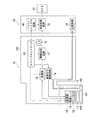
図1は、本実施形態である電子内視鏡装置のブロック図である。 FIG. 1 is a block diagram of an electronic endoscope apparatus according to this embodiment.
電子内視鏡装置は、その挿入部分が体内へ挿入されるビデオスコープ10と、プロセッサ30とを備え、ビデオスコープ10はプロセッサ30に着脱自在に接続される。プロセッサ30には、モニタ80が接続されている。
The electronic endoscope apparatus includes a
プロセッサ30は、放電ランプなどで構成される光源装置34を備える。光源装置34から放射される照明光は、集光レンズ(図示せず)を介して、ビデオスコープ10内に設けられたライトガイド11に入射する。ライトガイド11に入射した光は、ライトガイド11内部を通ってスコープ先端部10Tから射出し、配光レンズ14Aを介して被写体(観察対象)に照射される。
The
被写体に反射した照明光は、スコープ先端部に設けられたカバーガラス14B、対物レンズ13を通り、これによって、対物レンズ13後方に位置する撮像ユニット12のイメージセンサ52に被写体像が形成される。
The illumination light reflected by the subject passes through the cover glass 14B provided at the distal end of the scope and the
イメージセンサ52は、X−Yアドレス型撮像素子であり、ここではCMOSセンサによって構成されている。イメージセンサ52で生じる1フィールドもしくは1フレーム分の画像信号は、撮像素子駆動回路19によって所定の読み出し時間間隔(例えば、1/60秒もしくは1/30秒間隔)に従い読み出される。イメージセンサ52には、Cy、Ye、G、Mg、あるいはR、G、Bなどの複数の色要素を配列させた色フィルタが配設されており、カラー撮像方式として同時単板式が適用されている。
The
イメージセンサ52から読み出された画素信号は、デジタル化された後にシリアル信号に変換され、シリアルデータが、送信部56からビデオスコープ10の基端側(プロセッサ接続側)のコネクタ部10Cへ向けて送信される。
The pixel signal read from the
コネクタ部10Cには、スコープコントローラ15、受信部16、画像処理回路17、タイミングジェネレータ18、撮像素子駆動回路19などが設けられている。CPU、RAM、ROMなどを含むスコープコントローラ15は、コネクタ部10C内の各回路、そしてスコープ先端側の撮像ユニット12へ制御信号を送信し、スコープ動作全体を制御する。スコープ動作制御プログラムは、ROMに格納されている。
The connector unit 10C is provided with a
受信部16では、受信したシリアルデータをパラレルデータに変換するとともに、シリアルデータから画素データを取り出し、コネクタ部10Cの同期タイミングで再同期する。画像処理回路17では、送られてきたデジタル画素信号に対してホワイトバランス処理、ガンマ補正処理などの信号処理が施される。これにより、カラーデジタル画像信号が生成される。カラーデジタル画像信号は、プロセッサ30の後段処理回路32へ送られる。なお、プロセッサ30側に受信部を設け、画像処理するように構成してもよい。
The receiving
後段処理回路32では、輪郭強調などの画像処理が施される。そして、後段処理回路32から出力された画像信号が映像信号としてモニタ80に出力されることにより、観察画像が動画像としてモニタ80に表示される。
The
CPU、ROM、RAMなどを含むシステムコントロール回路40は、光源装置34などへ制御信号を出力し、プロセッサ30全体の動作を制御する。プロセッサ制御に関するプログラムは、ROMにあらかじめ格納されている。また、システムコントロール回路40は、スコープコントローラ15との間で相互通信可能である。
A
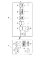
次に、図2〜5を用いて、ビデオスコープの先端側に設けられた送信部、プロセッサ側に設けられた受信部の構成を説明する。 Next, configurations of a transmission unit provided on the distal end side of the video scope and a reception unit provided on the processor side will be described with reference to FIGS.
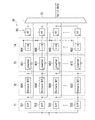
図2は、スコープ先端側の撮像ユニットと、プロセッサ接続側の受信部の詳細なブロック図である。図3は、送信部の一部構成を示す論理回路図である。 FIG. 2 is a detailed block diagram of the imaging unit on the distal end side of the scope and the receiving unit on the processor connection side. FIG. 3 is a logic circuit diagram showing a partial configuration of the transmission unit.
撮像ユニット12は、CMOS型のイメージセンサ52、A/D変換器53、パラレル/シリアル変換器54、同期信号付加回路55、送信部56を備え、1つのデバイスとして構成される。PLL回路51は、位相検出器、LPF、VOC、分周器を備えており、所定の周波数でクロック信号を出力可能である。PLL回路51は、受信部16に設けられたPLL回路68から出力される基準クロック信号に基づき、所定周波数のクロック信号を撮像ユニット12へ出力する。
The
イメージセンサ52から読み出された1フィールド/フレーム分のアナログ画素信号は、A/D変換器53によって所定ビット数のデジタルパラレル画素信号に変換される。そして、デジタルパラレル画素信号は、パラレル/シリアル変換器54によってデジタルシリアル信号に変換され、同期信号付加回路55において映像規格関連の同期信号が付加される。
The analog pixel signal for one field / frame read from the
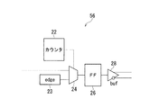
図3に示すように、送信部56は、カウンタ22、エッジ出力部23、セレクタ24、フリップフロップ26、バッファ回路28を備える。送信部56では、入力された一連のデジタルシリアル画素データの間に、所定のデータ幅(ビット数)の間隔で同期用のクロックデータ(以下、同期クロックという)ESを埋め込む。ここでは、20ビット間隔で同期クロックESを埋め込む。
As illustrated in FIG. 3, the
同期クロックESは、データ値「1」であるスタートビット(以下、同期データEDのS信号という)と、データ値「0」であるエンドビット(以下、同期データEDのE信号という)から構成され、周期が一定となるS信号、E信号の遷移エッジを検出することによって、受信側で画素データ抽出が可能となる。 The synchronous clock ES is composed of a start bit having a data value “1” (hereinafter referred to as an S signal of the synchronous data ED) and an end bit having a data value “0” (hereinafter referred to as an E signal of the synchronous data ED). By detecting the transition edge of the S signal and E signal with a constant period, pixel data can be extracted on the receiving side.
同期クロックESは、エッジを形成するデータによって構成されるデータであり、ここでは2ビットデータ「01」で構成される。シリアル画素データは、同期クロックESによって20ビットずつに区分され、これによりワード境界が規定される。同期クロックESの埋め込みは、カウンタ22によるビットカウントおよびセレクタ24による出力選択動作によって行われる。
The synchronous clock ES is data constituted by data forming an edge, and here is constituted by 2-bit data “01”. The serial pixel data is divided into 20 bits each by the synchronous clock ES, thereby defining a word boundary. The embedding of the synchronous clock ES is performed by a bit count by the
具体的には、伝送されるシリアル画素データを20ビット分カウントする度に、エッジ出力部23から同期クロックESを出力してビットデータ「01」を挿入し、エンベディットクロックのシリアルデータPDSを生成する。シリアルデータPDSは、高速の伝送レート(例えば600Mbps)で伝送される。
Specifically, every time 20 bits of serial pixel data to be transmitted are counted, the synchronous clock ES is output from the
一方、シリアルデータPDSを受信する受信部16は、CDR(Clock Data Recovery)回路62、FIFO64、受信回路70、同期信号付加回路82、出力回路84を備え、各回路は、水晶発振器66と接続されたPLL回路68から出力されるクロック信号に従って動作する。CDR回路62では、シリアルデータPDSの各ビットデータに対する同期再生が行われる。
On the other hand, the receiving
CDR回路62から出力されたシリアルデータPDSは、FIFO64を介して受信回路70へ送られる。受信回路70では、シリアルデータPDSがパラレルデータに変換されるとともに、シリアルデータPDSの中で20ビットから成るパラレル画素データの抽出処理が実行される。
The serial data PDS output from the
同期信号付加回路82では、抽出されたパラレル画素データに対して同期信号付加回路82において再同期されるとともに、同期信号が付加される。これによって、デジタル画像信号が出力回路84を経由して画像処理回路17に出力される。
In the synchronizing
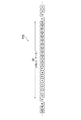
図4は、送信される1区画分のシリアルデータを示した図である。図5は、送信される1フレーム/フィールド分のシリアルデータを示した図である。ただし、図5では、1区画ずつ分けたパラレルデータ形式でシリアルデータを列表記している。 FIG. 4 is a diagram showing serial data for one section to be transmitted. FIG. 5 is a diagram showing serial data for one frame / field to be transmitted. However, in FIG. 5, serial data is represented in columns in a parallel data format divided into sections.
上述したように、シリアルデータPDSは、20ビットの画素データ(ここでは、0〜19番の番号を付けている)を1ブロックデータとし、その前後にスタートビット/エンドビット(S/E)を付けたデータ配列構造となっている。データ値「1」である同期データEDのS信号は、データ配列順に沿って20ビット画素データの前端に隣接する。一方、データ値「0」である同期データEDのE信号は、データ後端に隣接している。 As described above, the serial data PDS uses 20-bit pixel data (here, numbered 0 to 19) as one block data, and start / end bits (S / E) before and after that. The data array structure is attached. The S signal of the synchronization data ED having the data value “1” is adjacent to the front end of the 20-bit pixel data along the data arrangement order. On the other hand, the E signal of the synchronous data ED having the data value “0” is adjacent to the rear end of the data.
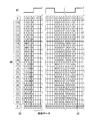
図5に示すように、シリアルデータPDSには、1フレーム/フィールド分の画像に相当する画素データと、ブランキング期間BTにおける画素データが含まれており、ブランキング期間BTの一部には、「1」のビット列(5ビット)と「0」のビット列(5ビット)とを合わせたシリアルデータBDを並べて埋め込んでいる。シリアルデータBDは、撮像ユニット12の同期信号付加回路55、あるいは送信部56において埋め込まれる。また、ブランキング期間BTには、ITU.BT656などの映像信号規格に従ったAVコードATが挿入されている。
As shown in FIG. 5, the serial data PDS includes pixel data corresponding to an image for one frame / field and pixel data in the blanking period BT. A part of the blanking period BT includes: Serial data BD, which is a combination of a bit string of “1” (5 bits) and a bit string of “0” (5 bits), is embedded side by side. The serial data BD is embedded in the synchronization
シリアルデータPDSが送信部56から受信部16へ出力されると、受信部16では、シリアルデータPDSの中から同期データEDを検出し、シリアル画素データを抽出する必要がある。すなわち、1区画分の画素データSDの境界を、シリアルデータPDSの中で判別しなければならない。
When the serial data PDS is output from the
本実施形態では、S信号、E信号を含めた22ビットのビットデータ(同期検出用データ)を複数作成し、ビットデータの前端、後端に同期クロックESのE信号、S信号がそれぞれ存在するビットデータを、画素データ抽出対象のビットデータと判断する。以下、具体的に説明する。 In this embodiment, a plurality of 22-bit bit data (synchronization detection data) including the S signal and the E signal are created, and the E signal and the S signal of the synchronization clock ES exist at the front end and the rear end of the bit data, respectively. The bit data is determined as the bit data from which pixel data is to be extracted. This will be specifically described below.
図6は、図2に示した受信回路の詳細なブロック図である。図7、図8は、同期判別用に生成される複数の同期検出用データを示した図である。ただし、図7、図8では、E信号、S信号を英小文字e、sで表している。 FIG. 6 is a detailed block diagram of the receiving circuit shown in FIG. 7 and 8 are diagrams illustrating a plurality of synchronization detection data generated for synchronization determination. However, in FIGS. 7 and 8, the E signal and the S signal are represented by lowercase letters e and s.
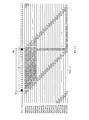
受信回路70は、シリアル/パラレル変換部71、同期判別部72、カウンタ73、閾値判別部74、セレクタ75を備えている。シリアル/パラレル変換部71、同期判別部72、カウンタ73、閾値判別部74は、それぞれ、22個のサブシリアル/パラレル変換回路701〜722、サブ同期判別器801〜822、サブカウンタ851〜872、サブ閾値判別回路901〜922から構成される。サブ同期判別器801〜822は、例えば、FPGAなどによって構成される。
The
シリアル/パラレル変換部71では、あらかじめ定められたデータ幅(以下、セグメントデータ幅という)でFIFO64から送られてくるシリアルデータを区切り、パラレルデータ変換処理が実行される。このとき、サブシリアル/パラレル変換回路701〜722では、シリアルデータの区切りを1ビットずつ順にシフトさせた上でパラレル変換処理が実行される。
In the serial /
図7には、サブシリアル/パラレル変換回路701〜722からサブ同期判別器801〜822に送られるパラレルデータが図示されており、各同期判定器におけるシリアルデータの区分け範囲がわかる。セグメントデータ幅は、データバス幅などに対応して定めることが可能である。ここでは、シリアル画素データの20ビットと、同期クロック(データ)ESの2ビットとを合わせた22ビットのデータ幅に定められている。
FIG. 7 shows parallel data sent from the sub-serial /
サブ同期判別器801とサブ同期判別器802とを比較すると、サブ同期判別器801のデータ区画T1に対し、サブ同期判別器802のデータ区画T2は1ビットずれている。同様に、サブ同期判定器803〜822において、順にデータ区画が1ビットずれている。
Comparing the
ところで、受信回路70では、送信部56側の同期クロックESの挿入タイミングを知らされていないため、送られてくるシリアルデータの同期クロックESの位置がどこに存在するか確定できない。しかしながら、あるタイミングで43ビットから成るデータを切り出し、そのデータから、データパターンの区切り範囲を1ビットずつ順次シフトさせた22通りのデータパターンを作成すれば、いずれか1つのデータ両端には、S信号とE信号がそれぞれ位置する。
By the way, since the receiving
すなわち、同期データEDのS信号、E信号がデータ両端にそれぞれ位置するパラレルデータが、サブ同期判別器801〜822のいずれかに存在し、そのタイミングのパラレルデータを選択することによって、画素データを再同期、出力させることができる。例えば、シリアルデータのビット位置FF、RRにそれぞれS信号、E信号が位置する場合、サブ同期判別器801のシリアル画素データを再同期対象の画素データとして抽出すればよい。
That is, the parallel data in which the S signal and the E signal of the synchronization data ED are located at both ends of the data exists in any of the
同期データEDがデータ前端、後端に位置するか否かの判断は、データ前端、後端のデータ値が、それぞれ「1」、[0]であるか否かを判断すればよい。しかしながら、画素データがデータ両端に位置している場合であっても、すなわち同期データ両端のビットデータ値が「1」、「0」である可能性もあり、一度の判定だけで同期データEDであると判定することはできない。 Whether or not the synchronization data ED is positioned at the data front end and the rear end may be determined by determining whether the data values at the data front end and the rear end are “1” and [0], respectively. However, even when the pixel data is located at both ends of the data, that is, there is a possibility that the bit data values at both ends of the synchronization data are “1” and “0”. It cannot be determined that there is.
一方、サブ同期判別器801〜822には、セグメントデータ幅に応じてパラレルデータが22ビットごと順次送られてくる。それらのパラレルデータも、シリアルデータに対する区分け範囲が1ビットずつずれている。したがって、サブ同期判別器801〜822の各々が、同期データEDの判定を繰り返し行い、データ両端のデータ値が同期データEDのデータ値と常に同一であれば、データ両端に同期データEDが位置しているパラレルデータとみなすことができる。
On the other hand, parallel data is sequentially sent to the
ここでは、サブ同期判別器801〜822各々が、送られてくるパラレルデータのデータ両端が同期データEDに対応したデータ値であるか否かを、22ビットのパラレルデータ変換の度に判断し、一致する場合の回数をカウントする。そして、サブ閾値判別回路901〜922は、カウント数が基準カウント数を超えているか否かを判断する。
Here, each of the
基準カウント数は、例えば、22ビットのパラレルデータに合わせて22回に設定することも可能であり、あるいはその半分の11〜22回の範囲、あるいは半分の11回以下にすることも可能である。内視鏡システムの構成やシリアルデータの伝送特性などに応じてあらかじめ基準カウント数を調整しながらシリアル画素データの抽出程度を実験的に確認し、好ましい基準カウント数を定めればよい。 The reference count number can be set to 22 times in accordance with, for example, 22-bit parallel data, or can be set to a range of 11 to 22 times, or half of 11 times or less. . A preferred reference count number may be determined by experimentally confirming the degree of serial pixel data extraction while adjusting the reference count number in advance according to the configuration of the endoscope system, serial data transmission characteristics, and the like.
セレクタ75は、基準カウント数を超えたパラレルデータのみ出力する。これによって同期データEDのS信号、E信号をそれぞれデータ前端、後端にもつシリアルデータが同期信号付加回路82(図2)へ送信される。その結果、同期ずれなく画素データが再同期されて出力される。
The
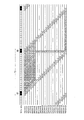
なお、データ両端の一方がS信号、他方がE信号であるか否かを判別する代わりに、データ前端部分、後端部分2ビットにおいて、同期データEDが存在するか否かを判別するようにしてもよい。この場合、所定のタイミングで45ビットのデータを区切り、データ両端が1ビットずつ順次シフトしている22通りのデータパターンが作成される。図8には、そのように作成された一連のデータパターンにおいて、24ビットのパラレルデータの区切り範囲T3を示している。この場合、データ両端の2ビットが同期クロックESと同じデータ値をもつか否か、すなわち、データ値「01」であるか否かを判断する。
Instead of determining whether one end of the data is an S signal and the other is an E signal, it is determined whether or not the synchronization data ED exists in the data front end portion and the
以上のように、内視鏡装置の使用開始時、すなわち、プロセッサが電源ONとなってビデオスコープ10がプロセッサ30に接続される、あるはいビデオスコープ10がプロセッサ30に接続されてからプロセッサ30の電源がON状態になると、シリアルデータが撮像ユニット12から受信部16に送信され、シリアルデータの中から画素データが抽出され、受信部16において再同期された画素データに基づく画像データが生成される。
As described above, when the use of the endoscope apparatus is started, that is, when the processor is turned on and the
しかしながら、電気メス使用といった内視鏡作業に起因してノイズが発生すると、受信部16において同期が外れる恐れがある。その場合、同期判定によって再同期させて画素データを再び抽出し、同期ずれを解消させなければならない。
However, if noise is generated due to endoscopic work such as using an electric knife, there is a risk that synchronization will be lost in the
画素データの再抽出を行う場合、同期クロックESを用いるのではなく、ブランキング期間に埋め込まれた同期検出用のブランキングデータに基づいて同期判定を行う。すなわち、同期判別部72において、ブランキング期間のシリアルデータに含まれるAVコードAT(図5参照)を検出し、これをトリガーとして同期判定を行う。
When re-extracting the pixel data, the synchronization determination is performed based on the blanking data for synchronization detection embedded in the blanking period, instead of using the synchronization clock ES. That is, the
サブ同期判別器801〜822は、AVコード検出によってブランキング期間を検出した後、ブランキング期間BTのシリアルデータを対象に同期判定を行う。具体的には、22ビットの同期検出用ブランキングデータと同一であるか否か、すなわち、2つ並んだシリアルデータBDを間に挟んでデータ両端にE信号、S信号が位置するデータ配列と等しいか否かをサブ同期判別器801〜822において判断する。
The
なお、同期検出用ブランキングデータの情報は、スコープコントローラ15から受信部16に送られており、これに基づいて同一性を判断する。また、スコープコントローラ15の制御によって、サブ同期判定器801〜802の動作を、同期データの位置判定からブランキングデータとの同一性判断に切り替える。なお、また、最初の画素データ抽出処理用の受信回路と、同期ずれ後の画素データ再抽出用受信回路とを、別々に設ける構成にしてもよい。
The information of the synchronization detection blanking data is sent from the
そして、同期検出用ブランキングデータと同一のデータ配列となるパラレルデータの場合、その回数をカウントする。そして、カウント数が基準閾値を超えた場合、そのパラレルデータがセレクタ75を経由して出力される。この場合、基準閾値は2である。ただし、カウントせずに1回の同期判定だけ行うことも可能である。
In the case of parallel data having the same data array as the synchronization detection blanking data, the number of times is counted. When the count number exceeds the reference threshold value, the parallel data is output via the
このように同期判定することにより、同期ずれなく画素データが再同期して出力される。なお、ここでは、ブランキング期間の所定の22ビットデータを対象にして同期判定を行っているが、ブランキング期間において他のデータサイズ、データ配列を対象にして同一性判断を行うことも可能であり、例えば、同期データEDを除くデータ配列を対象にすることも可能であり、あるいは、10ビットデータBTを対象に同一性を判断してもよい。 By determining the synchronization in this way, the pixel data is resynchronized and output without a synchronization error. Here, the synchronization determination is performed for predetermined 22-bit data in the blanking period, but it is also possible to perform the identity determination for other data sizes and data arrays in the blanking period. For example, it is possible to target a data array excluding the synchronization data ED, or the identity may be determined for the 10-bit data BT.
シリアルデータBDのデータ配列以外も同期判定可能であり、特に、「1」と「0」が交互に連続的に繰り返されるデータに基づいて同期判断することも可能である。 It is possible to determine synchronization other than the data arrangement of the serial data BD. In particular, it is also possible to determine synchronization based on data in which “1” and “0” are alternately and continuously repeated.
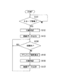
図9は、画素データ再同期処理のフローを示した図である。 FIG. 9 is a diagram illustrating a flow of pixel data resynchronization processing.
ビデオスコープ10がプロセッサ30に接続されると、図7、8を用いて説明した同期データ検出に基づいた同期判定処理が実行開始される。同期判定が終了するまでの間、すなわち、セレクタ75からパラレルデータが出力されない間、ブラック画面に対応した画像データを出力させ、オペレータを待機状態にする。そして、同期が確立されると、画像データ出力によって観察画像がモニタに表示される(S101〜S103)。
When the
画像データが出力されると、同期ずれが生じているか否かを検出するため、パラレルデータが出力されているサブパターン判別器において、データ両端に同期データEDが位置しているかモニタリングされる(S104)。そして、同期データEDと一致しないことが検出されると、ブランキング期間を検出し、ブランキング期間内におけるシリアルデータの配列と同一のデータ配列をもつパラレルデータを出力し、再同期させる(S105、S106)。 When the image data is output, in order to detect whether or not synchronization has occurred, it is monitored in the sub-pattern discriminator from which parallel data is output whether the synchronization data ED is located at both ends of the data (S104). ). When it is detected that the data does not match the synchronization data ED, a blanking period is detected, parallel data having the same data arrangement as the serial data arrangement in the blanking period is output and resynchronized (S105, S106).
ただし、同期判定を行っている間、ブラック画面に応じた画像データを出力する代わりに、フレームメモリに記憶させた同期ずれ前の画像データを表示させるようにしてもよい。 However, during the synchronization determination, instead of outputting the image data corresponding to the black screen, the image data before the synchronization shift stored in the frame memory may be displayed.
このように本実施形態によれば、ビデオスコープ10の先端部に設けられたイメージセンサ52から読み出される画素信号をデジタルシリアル化し、送信部56においては、20ビットのシリアル画素データの間に同期データEDとして同期信号S、同期信号Eから成る同期用クロックデータESを埋め込み、シリアルデータをスコープコネクタ部10Cへ送信する。
As described above, according to the present embodiment, the pixel signal read from the
一方、受信部16の受信回路70では、22ビットのセグメントデータ幅でシリアルデータを区切り、1ビットずつ区切り範囲を順次シフトさせた22個の同期検出用のパラレルデータを生成する。そして、受信回路70は、22個のパラレルデータの中から、同期データEDがデータ両端に位置するパラレルデータを選択、出力し、選択されたパラレルデータが再同期される。なお、22ビットのセグメントデータ幅で一度にシリアルデータを区切り、それから22個のパラレルデータを作成する代わりに、1ビットずつデータ潜り範囲を順次シフトさせながら、22個のパラレルデータを異なるタイミングで作成してもよい。
On the other hand, the receiving
8b/10b伝送方式のような変換テーブルを用いることなく、埋め込んだ同期クロックを正確に検知し、シリアル画素データを取り出すことができる。特に、スコープ先端部における回路構成としてはセレクタ等を設けるだけでよいため、スコープ先端部の回路構成が簡素化できる。また、受信部において、ワードアライナなどのワード境界を検知する回路を設ける必要がない。 Without using a conversion table as in the 8b / 10b transmission method, the embedded synchronous clock can be detected accurately and serial pixel data can be extracted. In particular, since it is only necessary to provide a selector or the like as the circuit configuration at the distal end portion of the scope, the circuit configuration at the distal end portion of the scope can be simplified. Further, it is not necessary to provide a circuit for detecting a word boundary such as a word aligner in the receiving unit.
一方、受信部における同期判定は、PLL回路を利用した構成とは相違するため、位相ロックのためのテスト用パターンを受信部へ向けて送信する必要もなく、さらに、シリアルデータと並走して同期クロックを送る必要もない。また、再同期させた後にノイズなどの影響で同期ずれが生じても、テスト用パターンの送信など、同期修正のための切り替え処理などをする必要がなく、瞬時に画像データ出力を回復することが可能となっている。 On the other hand, since the synchronization determination in the receiving unit is different from the configuration using the PLL circuit, it is not necessary to transmit a test pattern for phase lock to the receiving unit, and in addition, it runs in parallel with the serial data. There is no need to send a synchronous clock. In addition, even if synchronization is lost after resynchronization, there is no need to perform switching processing for synchronization correction, such as transmission of test patterns, and image data output can be recovered instantaneously. It is possible.
また、同期データ一致の回数をカウントし、最も早く閾値を超えるパラレルデータを選択するため、確実に同期データEDが両端に位置するパラレルデータを画素データとして抽出することができる。 Further, since the number of times of synchronization data coincidence is counted and the parallel data exceeding the threshold is selected earliest, the parallel data in which the synchronization data ED is positioned at both ends can be surely extracted as the pixel data.
複数のパラレルデータを同期検出用データとして生成し、その中から1つのパラレルデータを選択する回路構成を採用することにより、簡易な回路構成でデータ処理速度を落とすことなく画像信号処理を行うことができる。 By adopting a circuit configuration that generates a plurality of parallel data as synchronization detection data and selects one of the parallel data, image signal processing can be performed with a simple circuit configuration without reducing the data processing speed. it can.
また、本実施形態によれば、画素データを抽出後にノイズなどの影響で同期ずれが生じた場合、ブランキング期間を検出し、22ビットのセグメントデータ幅でシリアルデータを区切りながら、1ビットずつ区切り範囲を順次シフトさせて22個の同期検出用のパラレルデータを生成する。そして、ブランキング期間に埋め込まれた同期検出用データとデータ配列が等しいパラレルデータを選択し、出力する。 In addition, according to the present embodiment, when a synchronization error occurs due to noise or the like after the pixel data is extracted, the blanking period is detected, and the serial data is divided by the segment data width of 22 bits, and is divided bit by bit. The range is sequentially shifted to generate 22 pieces of parallel data for synchronization detection. Then, parallel data having the same data array as the synchronization detection data embedded in the blanking period is selected and output.
シリアル画素データのデータ配列は、観察画像の輝度、色相に依存するが、内視鏡観察画像の場合、偏った輝度レベル、色合いの画像エリアによって占められており、シリアル画素データの配列に偏りが生じることが多い。 The data arrangement of the serial pixel data depends on the luminance and hue of the observation image, but in the case of an endoscopic observation image, it is occupied by a biased luminance level and hue image area, and the serial pixel data arrangement is biased. Often occurs.
しかしながら、上述したように、ブランキング期間のシリアル画素データは、「1」のビット列と「0」のビット列を並べたシリアルデータBDに基づいた構成されている。そのため、DCバランスが安定し、シリアル画素データを対象に同期判定する場合に比べて、効果的に同期ずれを瞬時に解消することができる。特に、ビットデータ「1」ビットデータ「0」が交互に連続して繰り返されるデータを埋め込む場合、DCバランスの安定性は顕著であり、極めて有効である。また、再同期を行った後の同期判定であって観察画像を表示している状態のため、ブランキング期間を検出しやすい。 However, as described above, the serial pixel data in the blanking period is configured based on serial data BD in which a bit string of “1” and a bit string of “0” are arranged. Therefore, the DC balance is stable, and synchronization deviation can be effectively eliminated instantaneously as compared with the case where synchronization determination is performed on serial pixel data. In particular, when embedding data in which bit data “1” and bit data “0” are alternately and repeatedly embedded, the stability of the DC balance is remarkable and extremely effective. In addition, since it is a synchronization determination after resynchronization and the observation image is displayed, it is easy to detect the blanking period.
なお、1ビットずつ順次シフトさせるだけでなく、所定ビット数ずつ区切りをシフトさせて複数のデータを生成するようにしてもよい。また、プロセッサ接続時と途中で同期ずれが生じた場合いずれにおいても、同期データを用いて再同期してもよく、あるいは、ブランキング期間のデータを用いて再同期させてもよい。 In addition to sequentially shifting one bit at a time, a plurality of data may be generated by shifting a delimiter by a predetermined number of bits. Further, in any case where a synchronization shift occurs during the connection with the processor, resynchronization may be performed using synchronization data, or resynchronization may be performed using data in the blanking period.
10 ビデオスコープ
12 撮像ユニット
16 受信部
30 プロセッサ
56 送信部
70 受信回路
E 同期信号(同期データ)
S 同期信号(同期データ)
DESCRIPTION OF
S Sync signal (synchronous data)
Claims (6)
スコープ先端部に設けられ、前記撮像素子から読み出される画素信号をデジタルシリアル化した画素データに対し、ブランキング期間に同期検出用ブランキングデータを埋め込み、また、所定のデータ幅に従って同期データを埋め込んでシリアルデータを出力する送信部と、
スコープ基端側もしくは内視鏡プロセッサに設けられており、受信したシリアルデータにおける画素データを抽出する受信部とを備え、
前記受信部が、前記データ幅に前記同期データのビット数を加えたセグメントデータ幅に従い、ブランキング期間のシリアルデータを区切り、データ区切り範囲を所定ビットずつシフトさせた複数の同期検出用データを生成し、そして、前記複数の同期検出用データの中から、前記ブランキングデータに相当する同期検出用データを選択することを特徴とする内視鏡装置。 An image sensor provided at the distal end of the scope;
Provided at the distal end of the scope, the pixel data read out from the image sensor is digitally serialized, the blanking data for synchronization detection is embedded in the blanking period, and the synchronization data is embedded according to a predetermined data width. A transmission unit for outputting serial data;
Provided on the proximal side of the scope or in the endoscope processor, and having a receiving unit for extracting pixel data in the received serial data,
The receiver generates a plurality of synchronization detection data by delimiting serial data in the blanking period and shifting the data delimiter range by a predetermined bit according to a segment data width obtained by adding the number of bits of the synchronization data to the data width An endoscope apparatus that selects synchronization detection data corresponding to the blanking data from the plurality of synchronization detection data.
Priority Applications (1)
| Application Number | Priority Date | Filing Date | Title |
|---|---|---|---|
| JP2014248315A JP2016106902A (en) | 2014-12-08 | 2014-12-08 | Endoscope apparatus |
Applications Claiming Priority (1)
| Application Number | Priority Date | Filing Date | Title |
|---|---|---|---|
| JP2014248315A JP2016106902A (en) | 2014-12-08 | 2014-12-08 | Endoscope apparatus |
Publications (1)
| Publication Number | Publication Date |
|---|---|
| JP2016106902A true JP2016106902A (en) | 2016-06-20 |
Family
ID=56122416
Family Applications (1)
| Application Number | Title | Priority Date | Filing Date |
|---|---|---|---|
| JP2014248315A Pending JP2016106902A (en) | 2014-12-08 | 2014-12-08 | Endoscope apparatus |
Country Status (1)
| Country | Link |
|---|---|
| JP (1) | JP2016106902A (en) |
Cited By (1)
| Publication number | Priority date | Publication date | Assignee | Title |
|---|---|---|---|---|
| US11516420B2 (en) | 2018-04-04 | 2022-11-29 | Olympus Corporation | Imaging system and endoscope system |
-
2014
- 2014-12-08 JP JP2014248315A patent/JP2016106902A/en active Pending
Cited By (1)
| Publication number | Priority date | Publication date | Assignee | Title |
|---|---|---|---|---|
| US11516420B2 (en) | 2018-04-04 | 2022-11-29 | Olympus Corporation | Imaging system and endoscope system |
Similar Documents
| Publication | Publication Date | Title |
|---|---|---|
| CN102283625B (en) | Endoscope system | |
| JP5588949B2 (en) | Endoscope system and endoscope external control device | |
| JP2013078377A (en) | Endoscope system and external control device of endoscope | |
| JP5290480B1 (en) | Imaging apparatus and imaging system | |
| EP2575352A1 (en) | Endoscope system and external control device for endoscope | |
| US10284838B2 (en) | Method and apparatus for transmitting images captured by first and second image sensors | |
| JP6049554B2 (en) | Image processing device | |
| US8279274B2 (en) | Receiving apparatus, transmitting apparatus and in-vivo information acquiring apparatus | |
| JP6034703B2 (en) | Conversion circuit, image processing apparatus, and conversion method | |
| JP2015080702A (en) | Endoscope device | |
| JP5137372B2 (en) | Image processing system and endoscope system | |
| JP2016111557A (en) | Endoscope apparatus | |
| JP4353828B2 (en) | False detection prevention circuit | |
| JP2016106902A (en) | Endoscope apparatus | |
| US20090278983A1 (en) | Digital video signal transmitter and receiver and including system | |
| KR100789680B1 (en) | Clock Generation Circuit and Teletext Broadcasting Data Sampling Circuit | |
| JP2014110843A (en) | Endoscope device | |
| JP2008219773A (en) | Transmitting device, receiving device, and optical communication method | |
| JP2014110855A (en) | Endoscope device | |
| JP2020088671A (en) | Imaging device and signal processing method in the device | |
| US8913472B2 (en) | Data capture device and method thereof | |
| JP5551978B2 (en) | Noise filter | |
| JP2005278088A (en) | External synchronization signal generation circuit and phase difference measurement circuit | |
| JP2007165955A (en) | Vertical synchronizing signal generator | |
| JP2006203473A (en) | Synchronization detection circuit |