JP2016100268A - Planar lighting device - Google Patents
Planar lighting device Download PDFInfo
- Publication number
- JP2016100268A JP2016100268A JP2014237800A JP2014237800A JP2016100268A JP 2016100268 A JP2016100268 A JP 2016100268A JP 2014237800 A JP2014237800 A JP 2014237800A JP 2014237800 A JP2014237800 A JP 2014237800A JP 2016100268 A JP2016100268 A JP 2016100268A
- Authority
- JP
- Japan
- Prior art keywords
- light
- light source
- circuit board
- guide plate
- film
- Prior art date
- Legal status (The legal status is an assumption and is not a legal conclusion. Google has not performed a legal analysis and makes no representation as to the accuracy of the status listed.)
- Granted
Links
- 239000012787 coverlay film Substances 0.000 claims abstract description 68
- 239000010408 film Substances 0.000 claims description 44
- 238000005286 illumination Methods 0.000 claims description 28
- 239000004020 conductor Substances 0.000 claims description 26
- OAICVXFJPJFONN-UHFFFAOYSA-N Phosphorus Chemical compound [P] OAICVXFJPJFONN-UHFFFAOYSA-N 0.000 claims description 18
- 239000013039 cover film Substances 0.000 claims description 4
- 230000031700 light absorption Effects 0.000 claims description 2
- 230000003287 optical effect Effects 0.000 abstract description 26
- 230000009467 reduction Effects 0.000 abstract description 4
- 230000007423 decrease Effects 0.000 abstract description 2
- 239000010410 layer Substances 0.000 description 24
- 239000000463 material Substances 0.000 description 10
- 239000000126 substance Substances 0.000 description 4
- 230000006872 improvement Effects 0.000 description 3
- 239000011248 coating agent Substances 0.000 description 2
- 238000000576 coating method Methods 0.000 description 2
- 230000000694 effects Effects 0.000 description 2
- 238000000295 emission spectrum Methods 0.000 description 2
- 239000004973 liquid crystal related substance Substances 0.000 description 2
- 238000000034 method Methods 0.000 description 2
- 230000008569 process Effects 0.000 description 2
- 230000001737 promoting effect Effects 0.000 description 2
- 239000012790 adhesive layer Substances 0.000 description 1
- 230000008901 benefit Effects 0.000 description 1
- 238000010586 diagram Methods 0.000 description 1
- 238000009792 diffusion process Methods 0.000 description 1
- 230000002452 interceptive effect Effects 0.000 description 1
- 230000007257 malfunction Effects 0.000 description 1
- 239000002184 metal Substances 0.000 description 1
- 230000001681 protective effect Effects 0.000 description 1
- 229920005989 resin Polymers 0.000 description 1
- 239000011347 resin Substances 0.000 description 1
- 239000000758 substrate Substances 0.000 description 1
- 229920003002 synthetic resin Polymers 0.000 description 1
- 239000000057 synthetic resin Substances 0.000 description 1
Images


Classifications
-
- H—ELECTRICITY
- H05—ELECTRIC TECHNIQUES NOT OTHERWISE PROVIDED FOR
- H05K—PRINTED CIRCUITS; CASINGS OR CONSTRUCTIONAL DETAILS OF ELECTRIC APPARATUS; MANUFACTURE OF ASSEMBLAGES OF ELECTRICAL COMPONENTS
- H05K1/00—Printed circuits
- H05K1/02—Details
- H05K1/0274—Optical details, e.g. printed circuits comprising integral optical means
-
- G—PHYSICS
- G02—OPTICS
- G02B—OPTICAL ELEMENTS, SYSTEMS OR APPARATUS
- G02B6/00—Light guides; Structural details of arrangements comprising light guides and other optical elements, e.g. couplings
- G02B6/0001—Light guides; Structural details of arrangements comprising light guides and other optical elements, e.g. couplings specially adapted for lighting devices or systems
- G02B6/0011—Light guides; Structural details of arrangements comprising light guides and other optical elements, e.g. couplings specially adapted for lighting devices or systems the light guides being planar or of plate-like form
- G02B6/0066—Light guides; Structural details of arrangements comprising light guides and other optical elements, e.g. couplings specially adapted for lighting devices or systems the light guides being planar or of plate-like form characterised by the light source being coupled to the light guide
- G02B6/0073—Light emitting diode [LED]
-
- G—PHYSICS
- G02—OPTICS
- G02B—OPTICAL ELEMENTS, SYSTEMS OR APPARATUS
- G02B6/00—Light guides; Structural details of arrangements comprising light guides and other optical elements, e.g. couplings
- G02B6/0001—Light guides; Structural details of arrangements comprising light guides and other optical elements, e.g. couplings specially adapted for lighting devices or systems
- G02B6/0011—Light guides; Structural details of arrangements comprising light guides and other optical elements, e.g. couplings specially adapted for lighting devices or systems the light guides being planar or of plate-like form
- G02B6/0081—Mechanical or electrical aspects of the light guide and light source in the lighting device peculiar to the adaptation to planar light guides, e.g. concerning packaging
- G02B6/0086—Positioning aspects
- G02B6/009—Positioning aspects of the light source in the package
-
- G—PHYSICS
- G02—OPTICS
- G02B—OPTICAL ELEMENTS, SYSTEMS OR APPARATUS
- G02B6/00—Light guides; Structural details of arrangements comprising light guides and other optical elements, e.g. couplings
- G02B6/0001—Light guides; Structural details of arrangements comprising light guides and other optical elements, e.g. couplings specially adapted for lighting devices or systems
- G02B6/0011—Light guides; Structural details of arrangements comprising light guides and other optical elements, e.g. couplings specially adapted for lighting devices or systems the light guides being planar or of plate-like form
- G02B6/0081—Mechanical or electrical aspects of the light guide and light source in the lighting device peculiar to the adaptation to planar light guides, e.g. concerning packaging
- G02B6/0083—Details of electrical connections of light sources to drivers, circuit boards, or the like
-
- H—ELECTRICITY
- H05—ELECTRIC TECHNIQUES NOT OTHERWISE PROVIDED FOR
- H05K—PRINTED CIRCUITS; CASINGS OR CONSTRUCTIONAL DETAILS OF ELECTRIC APPARATUS; MANUFACTURE OF ASSEMBLAGES OF ELECTRICAL COMPONENTS
- H05K1/00—Printed circuits
- H05K1/18—Printed circuits structurally associated with non-printed electric components
- H05K1/189—Printed circuits structurally associated with non-printed electric components characterised by the use of a flexible or folded printed circuit
-
- H—ELECTRICITY
- H05—ELECTRIC TECHNIQUES NOT OTHERWISE PROVIDED FOR
- H05K—PRINTED CIRCUITS; CASINGS OR CONSTRUCTIONAL DETAILS OF ELECTRIC APPARATUS; MANUFACTURE OF ASSEMBLAGES OF ELECTRICAL COMPONENTS
- H05K2201/00—Indexing scheme relating to printed circuits covered by H05K1/00
- H05K2201/01—Dielectrics
- H05K2201/0104—Properties and characteristics in general
- H05K2201/0112—Absorbing light, e.g. dielectric layer with carbon filler for laser processing
-
- H—ELECTRICITY
- H05—ELECTRIC TECHNIQUES NOT OTHERWISE PROVIDED FOR
- H05K—PRINTED CIRCUITS; CASINGS OR CONSTRUCTIONAL DETAILS OF ELECTRIC APPARATUS; MANUFACTURE OF ASSEMBLAGES OF ELECTRICAL COMPONENTS
- H05K2201/00—Indexing scheme relating to printed circuits covered by H05K1/00
- H05K2201/10—Details of components or other objects attached to or integrated in a printed circuit board
- H05K2201/10007—Types of components
- H05K2201/10106—Light emitting diode [LED]
Abstract
Description
本発明は、液晶表示装置等の照明手段として用いられる面状照明装置に関するものである。 The present invention relates to a planar illumination device used as illumination means such as a liquid crystal display device.
今日、パーソナルコンピュータや携帯電話等の電子装置の表示デバイスとして、液晶表示装置と面状照明装置との組合せが、薄型化が容易であるという利点を有することから広く使用されている。又、近年の白色発光ダイオード(LED)の高性能化に伴い、面状照明装置のさらなる小型・薄型化及び低消費電力化を図るため、光源として白色LEDを使用した面状照明装置も一般的となっている。
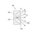
このような面状照明装置は、後述するように(図1参照)、対向する一対の主面の一方を光の出射面とする導光板と、導光板の入光面に対向して配置されるLEDと、LEDが実装される回路基板と、を備えている。LEDには、例えば、図3に示される白色LED100が使用される(例えば、特許文献1参照)。この白色LED100は、青色LEDチップ102が黄色蛍光体104によって、白色樹脂からなるランプハウス106に封止された構造を有するものである。図示のように、青色LEDチップ102は、ランプハウス106の長手方向の略中央部に配置されている。又、電極端子(図示省略)が、ランプハウス106の長手方向の両端に配置されている。そして、この電極端子が実装される回路基板には、フレキシブルプリント基板(FPC:Flexible Print Circuits)が広く用いられている。
Today, a combination of a liquid crystal display device and a planar illumination device is widely used as a display device for electronic devices such as personal computers and mobile phones because it has the advantage of being easily thinned. In addition, with the recent improvement in performance of white light emitting diodes (LEDs), a planar lighting device using a white LED as a light source is generally used in order to further reduce the size and thickness of the planar lighting device and reduce power consumption. It has become.
As will be described later (see FIG. 1), such a planar illumination device is disposed to face a light guide plate having one of a pair of opposed main surfaces as a light exit surface, and a light incident surface of the light guide plate. LED, and a circuit board on which the LED is mounted. For example, a
FPCは、導体層を保護するカバーレイフィルムを備えており、このカバーレイフィルムを白色とした、サイドライト方式の面状照明装置が提案されている(例えば、特許文献2参照)。この白色カバーレイフィルムは、フィルム基材の全面に白色反射層を形成したものであり、保護部材として機能すると共に光反射部材としても機能するものである。すなわち、表示デバイスの構造上、LEDの発光面と導光板の入光面との間に隙間が介在するような場合においても、この隙間が白色カバーレイフィルムで塞がれることで、LEDの発光面より出射された光がその隙間から外部に漏れる光を低減するものとなる。又、白色カバーレイフィルムによって反射した光は導光板の入光面から導光板に入射し、導光板の光の出射面の輝度が向上するものとなる。 The FPC includes a coverlay film that protects a conductor layer, and a sidelight type planar illumination device in which the coverlay film is white has been proposed (see, for example, Patent Document 2). This white coverlay film has a white reflective layer formed on the entire surface of a film substrate, and functions as a protective member as well as a light reflecting member. That is, even in the case where a gap is interposed between the light emitting surface of the LED and the light incident surface of the light guide plate due to the structure of the display device, the gap is blocked by the white coverlay film, so that the light emission of the LED Light emitted from the surface reduces light leaking outside through the gap. Further, the light reflected by the white coverlay film enters the light guide plate from the light incident surface of the light guide plate, and the brightness of the light output surface of the light guide plate is improved.
ところで、面状照明装置の点状光源として、図3に示されるような青色LEDチップ102と黄色蛍光体104とからなる白色LED100が使用される場合には、一般に、発光面100aからの光の出射方向前方、即ち、光軸と平行な方向に向かって出射される光L3と比べ、光軸に対して傾斜する方向に出射される光L2、L1は、黄色味を帯びる傾向がある。しかも、光軸との角度がより大きいL2よりもL1の方がより黄色味が強くなる。これは、青色LEDチップ102から出射された光が発光面100aに至るまでの距離、即ち、黄色蛍光体104を通過する光の経路が、L3<L2<L1と順に長くなることに起因するものである。又、光軸に対し傾斜した光L1、L2は、発光面100aから導光板の入光面に入射し、出射面の入光面寄りの領域から出射する傾向にある。このため、FPCのカバーレイフィルムに白色カバーレイフィルムを使用した場合には、導光板の出射面のうち入光面寄りの領域から出射する光が黄色味を帯び、これにより色むらが認識されるという不具合が生じる場合がある。
By the way, when the
一方で、面状照明装置には、照明性能の向上と共に薄型化の要請があるが、薄型化が進行するほど、上述の色むらの発生も顕著になる傾向がある。
本発明は、上記課題に鑑みてなされたものであり、その目的とするところは、面状照明装置の更なる薄型化を促進しつつ、色むらを軽減することにある。
On the other hand, the planar illumination device has a demand for thinning along with improvement in illumination performance. However, as the thinning progresses, the above-described color unevenness tends to become remarkable.
The present invention has been made in view of the above problems, and an object of the present invention is to reduce color unevenness while promoting further thinning of the planar lighting device.
(発明の態様)
以下の発明の態様は、本発明の構成を例示するものであり、本発明の多様な構成の理解を容易にするために、項別けして説明するものである。各項は、本発明の技術的範囲を限定するものではなく、発明を実施するための最良の形態を参酌しつつ、各項の構成要素の一部を置換し、削除し、又は、更に他の構成要素を付加したものについても、本願発明の技術的範囲に含まれ得るものである。
(Aspect of the Invention)
The following aspects of the present invention exemplify the configuration of the present invention, and will be described separately for easy understanding of various configurations of the present invention. Each section does not limit the technical scope of the present invention, and some of the components of each section are replaced, deleted, or further while referring to the best mode for carrying out the invention. Those to which the above components are added can also be included in the technical scope of the present invention.
(1)対向する一対の主面の一方を光の出射面とする導光板と、該導光板の入光面に対向して配置される点状光源と、該点状光源が実装される回路基板と、を含む面状照明装置であって、前記回路基板は、ベースフィルムと、該ベースフィルムの第1面に積層される第1導体層及び第1カバーレイフィルムと、該ベースフィルムの第2面に積層される第2導体層及び第2カバーフィルムとを含み、前記第1導体層には、前記点状光源の一対の電極端子が電気的に接続される一対のランド部を含み、前記第2カバーレイフィルムが、光吸収機能を有する要素を含んで構成され、かつ、前記回路基板を前記ベースフィルムの第1面側から平面視したときの、前記点状光源の発光面からの光の出射方向前方部分と、前記一対のランド部間の部分に、前記第2カバーレイフィルムが露出している面状照明装置(請求項1)。 (1) A light guide plate having one of a pair of opposed main surfaces as a light exit surface, a point light source disposed to face the light incident surface of the light guide plate, and a circuit on which the point light source is mounted A circuit board comprising: a base film; a first conductor layer and a first coverlay film laminated on a first surface of the base film; and a first of the base film. Including a second conductor layer and a second cover film laminated on two surfaces, the first conductor layer including a pair of land portions to which a pair of electrode terminals of the point light source are electrically connected, The second coverlay film is configured to include an element having a light absorption function, and the circuit board is viewed from the light emitting surface of the point light source when viewed from the first surface side of the base film. In the front part of the light emission direction and the part between the pair of land parts, Serial second planar lighting device coverlay film is exposed (claim 1).
本項に記載の面状照明装置においては、点状光源の発光面から光軸方向(点状光源の発光面に垂直な方向)に向かって出射された光は、導光板の入光面に入射し、導光板内を進行する過程で適切に光路変更され、対向する一対の主面の一方である出射面から出射される。一方、点状光源の発光面から光軸方向に対し傾斜する方向に向かって出射された光のうち、回路基板をベースフィルムの第1面側から平面視したときの、点状光源の発光面からの光の出射方向前方部分と、一対のランド部間の部分とに進行する光は、回路基板の当該部分に露出する第2カバーレイフィルムに吸収される。従って、導光板の入光面に入射する光のうち、点状光源の発光面から光軸に対して傾斜する方向に出射される光の比率が減少し、その結果、導光板の出射面から出射される光に占める、点状光源の発光面から光軸方向に向かって出射された光の比率が増大することとなる。 In the planar illumination device described in this section, light emitted from the light emitting surface of the point light source toward the optical axis direction (direction perpendicular to the light emitting surface of the point light source) is incident on the light incident surface of the light guide plate. Incident light is appropriately changed in the process of traveling through the light guide plate, and is emitted from an exit surface that is one of a pair of opposing main surfaces. On the other hand, of the light emitted from the light emitting surface of the point light source toward the direction inclined with respect to the optical axis direction, the light emitting surface of the point light source when the circuit board is viewed in plan from the first surface side of the base film The light traveling to the front part in the light emission direction from the light and the part between the pair of land parts is absorbed by the second coverlay film exposed at the part of the circuit board. Therefore, the ratio of the light emitted from the light emitting surface of the point light source in the direction inclined with respect to the optical axis among the light incident on the light incident surface of the light guide plate is reduced, and as a result, from the light emitting surface of the light guide plate. The proportion of the light emitted from the light emitting surface of the point light source toward the optical axis direction in the emitted light increases.
(2)上記(1)項において、前記点状光源が、発光チップと蛍光体とを有し、前記第2カバーレイフィルムが、少なくとも前記蛍光体が発光する光を吸収する要素を含んで構成されている面状照明装置(請求項2)。
本項に記載の面状照明装置は、点状光源が発光チップと蛍光体とを有するものであることから、発光チップの光の色と、この光を吸収した蛍光体が発光する光の色との混色により、所定の色に見える発光スペクトルを実現するものである。具体例としては、発光チップの青色光と、黄色蛍光体が発光する黄色光との混色による白色に発光する白色LEDが挙げられる。白色LEDの場合には、前述のように、発光チップと蛍光体とを有する白色LEDの発光面から光軸に対して傾斜する方向に出射される光は、光軸との角度がより大きいほど、黄色味を帯びる傾向があり、かつ、導光板の出射面の入光面寄りの領域から出射する傾向がある。この黄色味を帯びた光が、回路基板をベースフィルムの第1面側から平面視したときの、点状光源の発光面からの光の出射方向前方部分と、一対のランド部間の部分に露出する第2カバーレイフィルムの、蛍光体が発光する光を吸収する要素によって吸収される。このため、導光板の入光面に入射する光のうち、点状光源の発光面から光軸に対して傾斜する方向に出射される黄色味を帯びた光の比率が、減少することとなる。
(2) In the above item (1), the point light source includes a light emitting chip and a phosphor, and the second coverlay film includes at least an element that absorbs light emitted from the phosphor. A planar lighting device (Claim 2).
In the surface illumination device described in this section, since the point light source includes the light emitting chip and the phosphor, the color of the light emitted from the light emitting chip and the color of the light emitted from the phosphor that has absorbed the light. To achieve an emission spectrum that looks like a predetermined color. As a specific example, there is a white LED that emits white light by mixing the blue light of the light emitting chip and the yellow light emitted from the yellow phosphor. In the case of a white LED, as described above, the light emitted from the light emitting surface of the white LED having the light emitting chip and the phosphor in the direction inclined with respect to the optical axis increases as the angle with the optical axis increases. There is a tendency to be yellowish, and there is a tendency to emit light from a region near the light incident surface of the light emitting plate. When the circuit board is viewed in plan from the first surface side of the base film, this yellowish light is emitted in the light emission direction front portion from the light emitting surface of the point light source and the portion between the pair of land portions. The exposed second coverlay film is absorbed by the element that absorbs light emitted by the phosphor. For this reason, among the light incident on the light incident surface of the light guide plate, the ratio of the yellowish light emitted in the direction inclined with respect to the optical axis from the light emitting surface of the point light source is reduced. .
なお、第2カバーレイフィルムの、蛍光体が発光する光を吸収する要素としては、例えば、第2カバーレイフィルムの材料に混入される、蛍光体が発光する光を吸収する素材や、無色透明又は黄色半透明な材料で形成された第2カバーレイフィルムの表面にコーティングされる、蛍光体が発光する光を吸収する素材等が挙げられる。
又、第2カバーレイフィルムの表面に蛍光体が発光する光を吸収する素材がコーティングされる構成を有する場合には、素材のコーティング範囲を、点状光源の前方の全ての領域に施す必要はなく、例えば、点状光源の発光面からの光の出射方向前方部分や、前記一対のランド部間の部分、すなわち、第2カバーレイフィルムの表面のうち、発光面から出射される光が当たり得る範囲にのみコーティングすることとしても良い。
In addition, as an element which absorbs the light which a fluorescent substance light-emits of a 2nd coverlay film, the material which absorbs the light which a phosphor emits light mixed in the material of a 2nd coverlay film, for example, and colorless and transparent Or the material etc. which are coated on the surface of the 2nd cover-lay film formed with the yellow translucent material, and absorb the light which a fluorescent substance light-emits are mentioned.
In addition, when the surface of the second coverlay film has a structure in which a material that absorbs light emitted from the phosphor is coated, it is necessary to apply the material coating range to all areas in front of the point light source. For example, light emitted from the light emitting surface among the front portion in the light emitting direction from the light emitting surface of the point light source or the portion between the pair of land portions, that is, the surface of the second coverlay film is not hit. It is good also as coating only in the range to obtain.
(3)上記(1)(2)項において、前記第2カバーレイフィルムが、黒色部材を含んで構成されている面状照明装置(請求項3)。
本項に記載の面状照明装置は、黒色部材によって、回路基板をベースフィルムの第1面側から平面視したときの、点状光源の発光面からの光の出射方向前方部分と、一対のランド部間の部分において、点状光源の発光面から光軸に対して傾斜する方向に出射される光が、第2カバーレイフィルムに吸収される。黒色部材は、例えば、第2カバーレイフィルムの材料に混入される黒色素材である場合や、無色透明又は黄色半透明な材料で形成された第2カバーレイフィルムの表面にコーティングされる黒色素材等が挙げられる。
(3) The planar illumination device according to (1) and (2) above, wherein the second coverlay film includes a black member.
The planar illumination device described in this section includes a black member and a front portion in the emission direction of light from the light emitting surface of the point light source when the circuit board is viewed in plan from the first surface side of the base film, and a pair of In the portion between the land portions, light emitted from the light emitting surface of the point light source in a direction inclined with respect to the optical axis is absorbed by the second coverlay film. The black member is, for example, a black material mixed in the material of the second coverlay film, a black material coated on the surface of the second coverlay film formed of a colorless transparent or yellow translucent material, etc. Is mentioned.
(4)上記(1)(2)項において、前記第2カバーレイフィルムが、青色部材を含んで構成されている面状照明装置。
本項に記載の面状照明装置は、上記(3)項の第2カバーレイフィルムの黒色部材を、青色部材に置換したものであり、これによって、点状光源の発光面から光軸に対して傾斜する方向に出射される光のうち、青色以外の光が吸収されるものである。特に、上記(2)項で言及したように、発光チップと蛍光体とを有する白色LEDが用いられる場合において、発光面から光軸に対して傾斜する方向に出射される黄色味を帯びた光が、第2カバーレイフィルムの青色部材によって吸収されることとなる。
(4) The planar illumination device according to (1) and (2), wherein the second coverlay film includes a blue member.
The planar illumination device described in this section is obtained by replacing the black member of the second coverlay film of the above (3) with a blue member, and thereby, from the light emitting surface of the point light source to the optical axis. Of the light emitted in the inclined direction, light other than blue is absorbed. In particular, as mentioned in the above item (2), in the case where a white LED having a light emitting chip and a phosphor is used, yellowish light emitted from the light emitting surface in a direction inclined with respect to the optical axis. Will be absorbed by the blue member of the second coverlay film.
(5)上記(1)から(4)項において、前記回路基板を平面視したときの、前記第2カバーレイフィルムの、前記点状光源の光の出射方向前方部分が、前記導光板の主面と重なるようにして配置されている面状照明装置(請求項4)。
本項に記載の面状照明装置は、回路基板を平面視したときの、第2カバーレイフィルムの、点状光源の光の出射方向前方部分が、導光板の主面と重なるようにして配置されるが、この部分は、上記(1)項で特定されるように、回路基板をベースフィルムの第1面側から平面視した状態で、第2カバーレイフィルムが露出している。すなわち、導光板の主面と重なる、点状光源の光の出射方向前方部分は、上記多層構造のうちの第2カバーレイフィルム以外の要素が存在せず、第2カバーレイフィルムが直接的に導光板の主面と重なることとなる。
(5) In the above items (1) to (4), when the circuit board is viewed in plan, the front portion of the second coverlay film in the light emitting direction of the point light source is the main light guide plate. A planar illumination device arranged so as to overlap a surface (Claim 4).
The planar illumination device described in this section is arranged so that the front portion of the light emission direction of the point light source of the second coverlay film overlaps the main surface of the light guide plate when the circuit board is viewed in plan. However, as specified in the above item (1), in this portion, the second coverlay film is exposed in a state in which the circuit board is viewed from the first surface side of the base film. That is, the light emission direction front portion of the light source that overlaps the main surface of the light guide plate has no elements other than the second coverlay film in the multilayer structure, and the second coverlay film directly It will overlap with the main surface of the light guide plate.
(6)上記(1)から(5)項において、前記ベースフィルムは、前記回路基板を平面視して、前記点状光源の発光面と略一致する前方端辺を有すると共に、前記点状光源と重なる位置に、前記前方端辺から後方へ向かって延びる切欠きが形成されている面状照明装置(請求項5)。
本項に記載の面状照明装置は、ベースフィルムが、回路基板を平面視して、点状光源の発光面と略一致する前方端辺を有すると共に、点状光源と重なる位置に、前方端辺から後方へ向かって延びる切欠きが形成されることで、ベースフィルムの第2面に積層される第2カバーレイフィルムは、回路基板をベースフィルムの第1面側から平面視したとき、前方端縁の更に前方及び切欠きの部分において露出する。換言すれば、ベースフィルムの前方端辺と切欠きとは、ベースフィルムの第2面側から見て、第2カバーレイフィルムによって覆われる。
(6) In the above items (1) to (5), the base film has a front end substantially coincident with a light emitting surface of the point light source in plan view of the circuit board, and the point light source A planar illumination device in which a notch extending rearward from the front end side is formed at a position overlapping with the front end side (Claim 5).
In the planar illumination device described in this section, the base film has a front end substantially coincident with the light emitting surface of the point light source in a plan view of the circuit board, and the front end at a position overlapping the point light source. By forming a notch extending rearward from the side, the second coverlay film laminated on the second surface of the base film has a front when the circuit board is viewed in plan from the first surface side of the base film. Exposed further forward and at the notch of the edge. In other words, the front edge and the notch of the base film are covered with the second coverlay film as viewed from the second surface side of the base film.
(7)上記(1)から(6)項において、前記第1カバーレイフィルムは、回路基板を前記ベースフィルムの第1面側から平面視して、点状光源の発光面と略一致する前方端辺を有すると共に、前記点状光源と重なる位置に、前記第1導体層の一対のランド部を露出させるための、前記前方端辺から後方へ向かって延びる切欠きが形成されている面状照明装置。
本項に記載の面状照明装置は、第1カバーレイフィルムは、回路基板をベースフィルムの第1面側から平面視して、点状光源の発光面と略一致する前方端辺を有すると共に、点状光源と重なる位置に形成された、前方端辺から後方へ向かって延びる切欠きにおいて、第1導体層の一対のランド部が露出する。このため、点状光源は、第1カバーレイフィルムに干渉することなく、その電極端子が一対のランド部に対して電気的に接続される。
(7) In the above items (1) to (6), the first coverlay film is a front substantially coincident with the light emitting surface of the point light source when the circuit board is viewed in plan from the first surface side of the base film. A planar shape having an end side and a notch extending rearward from the front end side for exposing the pair of land portions of the first conductor layer at a position overlapping the point light source. Lighting device.
In the planar illumination device described in this section, the first coverlay film has a front end substantially coincident with the light emitting surface of the point light source when the circuit board is viewed in plan from the first surface side of the base film. A pair of land portions of the first conductor layer are exposed at a notch formed in a position overlapping the point light source and extending rearward from the front end side. For this reason, the electrode terminal of the point light source is electrically connected to the pair of land portions without interfering with the first coverlay film.
本発明はこのように構成したので、面状照明装置の更なる薄型化を促進しつつ、色むらを軽減することが可能となる。 Since this invention was comprised in this way, it becomes possible to reduce color nonuniformity, promoting further thickness reduction of a planar illuminating device.
以下、本発明の実施の形態を図面に基づいて説明する。なお、従来技術と同一部分若しくは相当する部分については、適宜同一の符号を付して、詳しい説明を省略する。又、以下の説明における「上」、「下」の方向は、本説明における面状照明装置を平置きした状態での、上下方向を意味するものである。又、「前」、「後」の方向は、本説明における面状照明装置を平置きした状態での、点状光源の発光面からの光の出射方向前方と、その反対方向とを意味するものである。又、「略一致」は、完全一致状態に加え、寸法精度や組立制度上の誤差を許容した一致状態を含むものである。 Hereinafter, embodiments of the present invention will be described with reference to the drawings. In addition, about the same part as a prior art, or a part corresponding, the same code | symbol is attached | subjected suitably and detailed description is abbreviate | omitted. Further, the directions of “up” and “down” in the following description mean the vertical direction in the state where the planar lighting device in the present description is placed flat. In addition, the “front” and “rear” directions mean the front direction of light emission from the light emitting surface of the point light source and the opposite direction in the state where the planar illumination device in this description is placed flat. Is. The “substantially coincidence” includes not only a completely coincidence state but also a coincidence state that allows an error in dimensional accuracy and assembly system.
図1に示される面状照明装置10は、対向する一対の主面12a、12bのうちの一方を光の出射面12aとする導光板12と、導光板12の入光面12cに対向して配置される点状光源14としてのLEDと、点状光源14が実装される回路基板16とを備えている。又、導光板の出射面12aの上方には、拡散シートやプリズムシート等の光学シート類(図示省略)が配置され、出射面12aと対向する主面12bの下方には、反射シート(図示省略)が配置されている。更に、これらの構成要素が、例えば合成樹脂や金属からなるフレーム(図示省略)に収納されて、一体に構成されている。
A
導光板12は矩形平板状をなしている。図1の例では、対向する一対の主面12a、12bが互いに平行な平板状をなしているが、出射面12aから光が出射する範囲の厚みよりも、入光面12cが位置する端部の厚みが大きくなるように、いわゆる入光楔部が、入光面12cから所定の幅の範囲に設けられた導光板が用いられる場合もある。
点状光源14としてのLEDは、全体としては直方体状をなしており、電極端子を備える面底面と直交する側面が発光面14aとして構成された、いわゆるサイドビュータイプの白色LEDである。その具体的内部構造については、図3に示される白色LED100と同様であることから、詳しい説明を省略する。
The
The LED as the point
回路基板16は、いわゆる両面FPCであり、図2にも示されるように、ベースフィルム18と、ベースフィルム18の第1面(点状光源14が実装される実装面側の面)に積層される第1導体層20及び第1カバーレイフィルム22と、ベースフィルム18の第2面(第1面の裏面)に積層される第2導体層24及び第2カバーフィルム26とを含む、積層構造を有している。ベースフィルム18は、第1導体層20及び第2導体層24を担持するものであり、第1カバーレイフィルム22及び第2カバーレイフィルム26は、各々、第1導体層20及び第2導体層24を覆うものである。又、図示の例では、回路基板16には、二つの点状光源14が、それらの長手方向(図1(a)の上下方向)に沿って列状に実装されるように、回路基板16は平面視で長方形に形成されている。
The
第1カバーレイフィルム22は、概略櫛状に形成されている。具体的には、第1カバーレイフィルム22は、回路基板16をベースフィルムの第1面側から平面視して(図2(a)参照)、点状光源14の長手方向両脇に配置される両端部221と、点状光源14の後方に位置して、各両端部221をつなぐ連結部222とを有している。換言すれば、第1カバーレイフィルム22の前端部、すなわち、両端部221の前端部は、点状光源14の発光面と略一致する前方端辺223を有すると共に、点状光源14(図1)と重なる位置に、後述する第1導体層20の一対のランド部201を露出させるための、前方端辺223から後方へ向かって延びる切欠き224が形成されている。
The
第1導体層20には、点状光源14の一対の電極端子が電気的に接続される一対のランド部201が含まれている。一対のランド部201は、回路基板16をベースフィルム18の第1面側から平面視したとき(図2(a)参照)、第1カバーレイフィルム22の切欠き224から、直線状に配置された状態で露出している。
ベースフィルム18は、回路基板16を平面視して、点状光源14の発光面14aと略一致する前方端辺181を有すると共に、点状光源14と重なる位置に、前方端辺181から後方へ向かって延びる切欠き182が形成されている。換言すれば、ベースフィルム18は、点状光源14よりも前方部分と、第1導体層20の一対のランド部201の間とを除いた部分に配置されている。又、ベースフィルム18の前方端辺181と切欠き182とによって、ベースフィルム18の第1面に積層された第1導体層20の外形が定められる。そして、第1導体層20は、前方端辺181及び切欠き182に沿った不連続の外形となることで、第1導体層20には、点状光源14の一対の電極端子が電気的に接続される一対のランド部201が形成される。
The
The
第2導体層24は、点状光源14の接続形態(数、配列、電極端子の位置等)に応じて、適宜パターン化されて構成されている。又、第2導体層24はベースフィルム18の第2面に積層されているが、ベースフィルム18の第1面に積層された第1導体層20とは、ベースフィルム18を厚み方向に貫通するスルーホール(図示省略)を介して、電気的に接続されている。
The
第2カバーレイフィルム26は、全可視光を吸収する黒色部材から構成されている。又、第2カバーレイフィルム26の平面視における外形は、回路基板16の外形(図2(a)参照)と略一致する形状に構成されている。そして、上述したベースフィルム18及び第1カバーレイフィルム22の外形との関係から、回路基板16をベースフィルム18の第1面側から平面視したとき、点状光源14の発光面14a(図1参照)からの光の出射方向前方部分と、一対のランド部201間の部分に、第2カバーレイフィルム26が露出することとなる。
The
図1には、導光板12の入光面12cと、第2カバーレイフィルム26の前方端辺261との位置関係が示されている。図1から理解されるように、回路基板16を平面視したときの、第2カバーレイフィルム26の、点状光源14の光の出射方向前方部分が、導光板12の主面12a、12bと重なるようにして配置される。そして、第2カバーレイフィルム26の、点状光源14の光の出射方向前方部分と、導光板12の主面12a、12bとの重合部分において、第2カバーレイフィルム26は、導光板12の主面12bに対して、例えば両面テープを介して接着固定される。
なお、図示は省略するが、点状光源14の数は図示の二つないし複数に限定されるものではなく、単数であっても良い。又、図1の例では、回路基板16は導光板12の出射面12aと対向する主面12b側に配置されているが、必要に応じて、回路基板16を出射面12a側に配置することとしても良い。
FIG. 1 shows the positional relationship between the
In addition, although illustration is abbreviate | omitted, the number of the point
さて、上記構成をなす、本発明の実施の形態によれば、次のような作用効果を得ることが可能である。
すなわち、点状光源14の発光面14aから光軸方向(点状光源の発光面に垂直な方向)に向かって出射された光(図3の符号L3参照)は、導光板12の入光面12cに入射し、導光板12内を進行する過程で適切に光路変更され、出射面12aから出射される。一方、点状光源14の発光面14aから光軸方向に対し傾斜する方向に向かって出射された光(図3の符号L1、L2参照)のうち、点状光源14が実装される回路基板16をベースフィルム18の第1面側から平面視したときの(図1(a)、図2(a)参照)、点状光源14の発光面14cからの光の出射方向前方部分と、一対のランド部201間の部分に進行する光は、回路基板14の当該部分に露出する第2カバーレイフィルム26に吸収される。従って、導光板12の入光面12cに入射する光のうち、点状光源14の発光面14cから光軸に対して傾斜する方向に出射される光の比率が減少し、その結果、導光板14の出射面12aから出射される光に占める、点状光源12の発光面12aから光軸方向に向かって出射された光の比率が増大することとなる。
Now, according to the embodiment of the present invention configured as described above, the following operational effects can be obtained.
That is, the light emitted from the
そして、点状光源14が、図3に示されるものと同様に青色LEDチップ102と黄色蛍光体104とを有するものであることから、青色LEDチップ102の青色光と、この光を吸収した黄色蛍光体104が発光する黄色光との混色により、白色に見える発光スペクトルを実現するものである。そして、点状光源14の発光面14aから光軸に対して傾斜する方向に出射される光は、光軸との角度がより大きいほど、黄色味を帯びる傾向があり、かつ、導光板12の出射面12aの入光面12c寄りの領域から出射する傾向がある。この黄色味を帯びた光が、回路基板14をベースフィルム18の第1面側から平面視したときの、点状光源14の発光面14aからの光の出射方向前方部分と、一対のランド部201間の部分に露出する、黒色部材から構成された第2カバーレイフィルム26によって吸収される。このため、導光板12の入光面12cに入射する光のうち、点状光源14の発光面14aから光軸に対して傾斜する方向に出射される黄色味を帯びた光(図3の符号L1、L2参照)の比率が、減少することとなる。その結果、面状照明装置10の色むらを軽減することが可能となり、面状照明装置10の更なる薄型化を促進することが可能となる。
And since the point
なお、応用例として、第2カバーレイフィルム26を、全可視光を吸収する黒色部材ではなく、少なくとも黄色光、(点状光源14を構成する、図3に示される白色LED100の黄色蛍光体104が発光する色)を吸収する性質を有する部材で構成することとしても良い。一例として、青色光以外の光を吸収する青色部材からなる、青色カバーレイフィルムを用いることも可能である。この場合には、点状光源14の発光面14aから光軸に対して傾斜する方向に出射される光から黄色味が減少した状態で、導光板12の入光面12cに入射して、出射面12aからの出射光に加わることとなる。その結果、面状照明装置10の色むらの低減と共に、輝度の向上が期待できることとなる。
As an application example, the
又、本発明の実施の形態に係る面状照明装置10は、回路基板16を平面視したときの、第2カバーレイフィルム26の、点状光源14の光の出射方向前方部分が、導光板12の主面12a、12bと重なるようにして配置されるが、この部分は、上記のごとく、回路基板16をベースフィルム18の第1面側から平面視した状態で、第2カバーレイフィルム26が露出している。すなわち、回路基板16の当該部分は、上記多層構造のうちの第2カバーレイフィルム26以外の要素が存在せず、第2カバーレイフィルム26が直接的に導光板12の主面12a、12bと重なることとなる。このため、回路基板16と導光板12との重合部分における厚みは、導光板12の厚みに第2カバーフィルム26の厚みを加えたもの(若しくはこれに両者を固定する両面テープ等の接着層の厚みを加えたもの)に収まることとなり、面状照明装置10の更なる薄型化を促進することが可能となる。
Further, in the
又、ベースフィルム18が、回路基板16を平面視して、点状光源14の発光面14aと略一致する前方端辺181を有すると共に、点状光源14と重なる位置に、前方端辺181から後方へ向かって延びる切欠き182が形成されることで、ベースフィルム18の第2面に積層される第2カバーレイフィルム26は、回路基板16をベースフィルムの第1面側から平面視したとき、前方端縁181の更に前方及び切欠き182の部分において露出し、上記作用効果が得られるものである。
The
10 面状照明装置、12導光板、12a:出射面、12b:出射面と対向する主面、12c:入光面、14:点状光源、16:回路基板、 18:ベースフィルム、 181:前方端辺、 182:切欠き、 20:第1導体層、 201:一対のランド部、 22:第1カバーレイフィルム、 221:両端部、 222:連結部、 223:前方端辺、 224:切欠き、 24:第2導体層、 26:第2カバーレイフィルム、 100:白色LED、102:青色LEDチップ、104:黄色蛍光体
DESCRIPTION OF
Claims (5)
前記回路基板は、ベースフィルムと、該ベースフィルムの第1面に積層される第1導体層及び第1カバーレイフィルムと、該ベースフィルムの第2面に積層される第2導体層及び第2カバーフィルムとを含み、
前記第1導体層には、前記点状光源の一対の電極端子が電気的に接続される一対のランド部を含み、
前記第2カバーレイフィルムが、光吸収機能を有する要素を含んで構成され、
かつ、前記回路基板を前記ベースフィルムの第1面側から平面視したときの、前記点状光源の発光面からの光の出射方向前方部分と、前記一対のランド部間の部分に、前記第2カバーレイフィルムが露出していることを特徴とする面状照明装置。 A light guide plate having one of a pair of opposing main surfaces as a light emission surface, a point light source disposed to face the light incident surface of the light guide plate, a circuit board on which the point light source is mounted, A planar lighting device comprising:
The circuit board includes a base film, a first conductor layer and a first coverlay film laminated on the first surface of the base film, a second conductor layer and a second layer laminated on the second surface of the base film. Including a cover film,
The first conductor layer includes a pair of land portions to which a pair of electrode terminals of the point light source are electrically connected,
The second coverlay film is configured to include an element having a light absorption function,
And, when the circuit board is viewed in plan from the first surface side of the base film, the first portion in the light emission direction from the light emitting surface of the point light source and the portion between the pair of land portions, 2. A planar illumination device, wherein the coverlay film is exposed.
前記第2カバーレイフィルムが、少なくとも前記蛍光体が発光する光を吸収する要素を含んで構成されていることを特徴とする請求項1記載の面状照明装置。 The point light source has a light emitting chip and a phosphor,
The planar illumination device according to claim 1, wherein the second coverlay film includes at least an element that absorbs light emitted from the phosphor.
Priority Applications (2)
| Application Number | Priority Date | Filing Date | Title |
|---|---|---|---|
| JP2014237800A JP6220765B2 (en) | 2014-11-25 | 2014-11-25 | Surface lighting device |
| US14/944,949 US9655234B2 (en) | 2014-11-25 | 2015-11-18 | Planar illumination device |
Applications Claiming Priority (1)
| Application Number | Priority Date | Filing Date | Title |
|---|---|---|---|
| JP2014237800A JP6220765B2 (en) | 2014-11-25 | 2014-11-25 | Surface lighting device |
Publications (2)
| Publication Number | Publication Date |
|---|---|
| JP2016100268A true JP2016100268A (en) | 2016-05-30 |
| JP6220765B2 JP6220765B2 (en) | 2017-10-25 |
Family
ID=56011658
Family Applications (1)
| Application Number | Title | Priority Date | Filing Date |
|---|---|---|---|
| JP2014237800A Active JP6220765B2 (en) | 2014-11-25 | 2014-11-25 | Surface lighting device |
Country Status (2)
| Country | Link |
|---|---|
| US (1) | US9655234B2 (en) |
| JP (1) | JP6220765B2 (en) |
Families Citing this family (5)
| Publication number | Priority date | Publication date | Assignee | Title |
|---|---|---|---|---|
| US10107955B2 (en) * | 2015-04-27 | 2018-10-23 | Boe Technology Group Co., Ltd. | Display backlight module having double-side adhesive blocks |
| CN111720760A (en) * | 2016-08-26 | 2020-09-29 | 美蓓亚三美株式会社 | Planar lighting device and substrate |
| US10627568B2 (en) * | 2016-12-13 | 2020-04-21 | Minebea Mitsumi Inc. | Planar illumination device and method of manufacturing planar illumination device |
| CN109656057A (en) * | 2017-10-11 | 2019-04-19 | 群创光电股份有限公司 | Backlight module and display equipment comprising it |
| JP2019120757A (en) * | 2017-12-28 | 2019-07-22 | 株式会社ジャパンディスプレイ | Display |
Citations (2)
| Publication number | Priority date | Publication date | Assignee | Title |
|---|---|---|---|---|
| US20080158470A1 (en) * | 2007-01-03 | 2008-07-03 | Samsung Sdi Co., Ltd. | Flexible circuit board and liquid crystal display having the same |
| JP2013065404A (en) * | 2011-09-15 | 2013-04-11 | Minebea Co Ltd | Planar illumination apparatus |
Family Cites Families (11)
| Publication number | Priority date | Publication date | Assignee | Title |
|---|---|---|---|---|
| JP2003331628A (en) * | 2002-03-05 | 2003-11-21 | Seiko Epson Corp | Lighting device, liquid crystal device, and electronic device |
| WO2006087863A1 (en) * | 2005-02-18 | 2006-08-24 | Minebea Co., Ltd. | Planar illumination device |
| JP4311454B2 (en) * | 2006-06-05 | 2009-08-12 | エプソンイメージングデバイス株式会社 | Lighting device, liquid crystal device, and electronic device |
| JP2008170739A (en) * | 2007-01-12 | 2008-07-24 | Hitachi Displays Ltd | Liquid crystal display device |
| KR100957411B1 (en) * | 2008-02-05 | 2010-05-11 | 엘지이노텍 주식회사 | Light emitting apparatus |
| US8931943B2 (en) * | 2011-12-22 | 2015-01-13 | Minebea Co., Ltd. | Spread illuminating apparatus |
| JP5893912B2 (en) | 2011-12-22 | 2016-03-23 | ミネベア株式会社 | Surface lighting device |
| JP5973171B2 (en) * | 2012-01-20 | 2016-08-23 | ミネベア株式会社 | Surface lighting device |
| JP6025444B2 (en) * | 2012-08-03 | 2016-11-16 | ミネベア株式会社 | Surface lighting device |
| JP5440989B1 (en) | 2013-02-25 | 2014-03-12 | ミネベア株式会社 | Surface lighting device |
| JP6199761B2 (en) * | 2014-01-31 | 2017-09-20 | ミネベアミツミ株式会社 | Surface lighting device |
-
2014
- 2014-11-25 JP JP2014237800A patent/JP6220765B2/en active Active
-
2015
- 2015-11-18 US US14/944,949 patent/US9655234B2/en active Active
Patent Citations (2)
| Publication number | Priority date | Publication date | Assignee | Title |
|---|---|---|---|---|
| US20080158470A1 (en) * | 2007-01-03 | 2008-07-03 | Samsung Sdi Co., Ltd. | Flexible circuit board and liquid crystal display having the same |
| JP2013065404A (en) * | 2011-09-15 | 2013-04-11 | Minebea Co Ltd | Planar illumination apparatus |
Also Published As
| Publication number | Publication date |
|---|---|
| US9655234B2 (en) | 2017-05-16 |
| US20160150640A1 (en) | 2016-05-26 |
| JP6220765B2 (en) | 2017-10-25 |
Similar Documents
| Publication | Publication Date | Title |
|---|---|---|
| JP6220765B2 (en) | Surface lighting device | |
| CN107544111B (en) | Planar lighting device | |
| TWI544241B (en) | Display device | |
| JP6303646B2 (en) | Surface light source device | |
| JPWO2006087863A1 (en) | Area lighting device | |
| JP6284277B2 (en) | Surface lighting device | |
| US10851979B2 (en) | Backlight lamp bar, backlight module and display device | |
| JP2009026614A (en) | Surface light-emitting device, and display | |
| JP2019125519A (en) | Luminaire and display device | |
| US20110205453A1 (en) | Illumination device, surface illuminant device, display device, and television receiver | |
| TW201643920A (en) | Backlight module and lighting keyboard using the same | |
| JP2011141439A (en) | Liquid crystal display device | |
| JP2011096523A (en) | Spread illuminating apparatus | |
| JP2018181630A (en) | Back light | |
| US10082615B2 (en) | Planar illumination apparatus | |
| JP2011096522A (en) | Spread illuminating apparatus | |
| US11294116B2 (en) | Display device based on diffusion film and electronic device | |
| TWI580893B (en) | Light emitting module and display device | |
| JP6709768B2 (en) | Area lighting device | |
| JP6046015B2 (en) | Surface lighting device | |
| TWI437327B (en) | Back-light module | |
| CN110609413A (en) | Illumination device and display device | |
| JP2009238406A (en) | Back light unit and reflective sheet | |
| US10120122B2 (en) | Planar lighting device with external connection section | |
| US20160010810A1 (en) | Illumination device |
Legal Events
| Date | Code | Title | Description |
|---|---|---|---|
| A621 | Written request for application examination |
Free format text: JAPANESE INTERMEDIATE CODE: A621 Effective date: 20160511 |
|
| A977 | Report on retrieval |
Free format text: JAPANESE INTERMEDIATE CODE: A971007 Effective date: 20170315 |
|
| A131 | Notification of reasons for refusal |
Free format text: JAPANESE INTERMEDIATE CODE: A131 Effective date: 20170322 |
|
| A521 | Request for written amendment filed |
Free format text: JAPANESE INTERMEDIATE CODE: A523 Effective date: 20170407 |
|
| TRDD | Decision of grant or rejection written | ||
| A01 | Written decision to grant a patent or to grant a registration (utility model) |
Free format text: JAPANESE INTERMEDIATE CODE: A01 Effective date: 20170913 |
|
| A61 | First payment of annual fees (during grant procedure) |
Free format text: JAPANESE INTERMEDIATE CODE: A61 Effective date: 20171002 |
|
| R150 | Certificate of patent or registration of utility model |
Ref document number: 6220765 Country of ref document: JP Free format text: JAPANESE INTERMEDIATE CODE: R150 |
|
| R250 | Receipt of annual fees |
Free format text: JAPANESE INTERMEDIATE CODE: R250 |