JP2016052012A - Semiconductor device and information processing device - Google Patents
Semiconductor device and information processing device Download PDFInfo
- Publication number
- JP2016052012A JP2016052012A JP2014176385A JP2014176385A JP2016052012A JP 2016052012 A JP2016052012 A JP 2016052012A JP 2014176385 A JP2014176385 A JP 2014176385A JP 2014176385 A JP2014176385 A JP 2014176385A JP 2016052012 A JP2016052012 A JP 2016052012A
- Authority
- JP
- Japan
- Prior art keywords
- interaction
- spin
- node
- circuit
- current
- Prior art date
- Legal status (The legal status is an assumption and is not a legal conclusion. Google has not performed a legal analysis and makes no representation as to the accuracy of the status listed.)
- Granted
Links
Images


Classifications
-
- G—PHYSICS
- G06—COMPUTING; CALCULATING OR COUNTING
- G06F—ELECTRIC DIGITAL DATA PROCESSING
- G06F13/00—Interconnection of, or transfer of information or other signals between, memories, input/output devices or central processing units
- G06F13/14—Handling requests for interconnection or transfer
- G06F13/16—Handling requests for interconnection or transfer for access to memory bus
- G06F13/1668—Details of memory controller
-
- G—PHYSICS
- G06—COMPUTING; CALCULATING OR COUNTING
- G06F—ELECTRIC DIGITAL DATA PROCESSING
- G06F13/00—Interconnection of, or transfer of information or other signals between, memories, input/output devices or central processing units
- G06F13/14—Handling requests for interconnection or transfer
- G06F13/16—Handling requests for interconnection or transfer for access to memory bus
- G06F13/1605—Handling requests for interconnection or transfer for access to memory bus based on arbitration
- G06F13/1652—Handling requests for interconnection or transfer for access to memory bus based on arbitration in a multiprocessor architecture
-
- G—PHYSICS
- G06—COMPUTING; CALCULATING OR COUNTING
- G06N—COMPUTING ARRANGEMENTS BASED ON SPECIFIC COMPUTATIONAL MODELS
- G06N7/00—Computing arrangements based on specific mathematical models
- G06N7/01—Probabilistic graphical models, e.g. probabilistic networks
-
- G—PHYSICS
- G11—INFORMATION STORAGE
- G11C—STATIC STORES
- G11C11/00—Digital stores characterised by the use of particular electric or magnetic storage elements; Storage elements therefor
- G11C11/02—Digital stores characterised by the use of particular electric or magnetic storage elements; Storage elements therefor using magnetic elements
- G11C11/16—Digital stores characterised by the use of particular electric or magnetic storage elements; Storage elements therefor using magnetic elements using elements in which the storage effect is based on magnetic spin effect
-
- G—PHYSICS
- G11—INFORMATION STORAGE
- G11C—STATIC STORES
- G11C14/00—Digital stores characterised by arrangements of cells having volatile and non-volatile storage properties for back-up when the power is down
- G11C14/0054—Digital stores characterised by arrangements of cells having volatile and non-volatile storage properties for back-up when the power is down in which the volatile element is a SRAM cell
- G11C14/0081—Digital stores characterised by arrangements of cells having volatile and non-volatile storage properties for back-up when the power is down in which the volatile element is a SRAM cell and the nonvolatile element is a magnetic RAM [MRAM] element or ferromagnetic cell
-
- G—PHYSICS
- G11—INFORMATION STORAGE
- G11C—STATIC STORES
- G11C5/00—Details of stores covered by group G11C11/00
- G11C5/06—Arrangements for interconnecting storage elements electrically, e.g. by wiring
- G11C5/08—Arrangements for interconnecting storage elements electrically, e.g. by wiring for interconnecting magnetic elements, e.g. toroidal cores
-
- G—PHYSICS
- G11—INFORMATION STORAGE
- G11C—STATIC STORES
- G11C7/00—Arrangements for writing information into, or reading information out from, a digital store
- G11C7/10—Input/output [I/O] data interface arrangements, e.g. I/O data control circuits, I/O data buffers
- G11C7/1006—Data managing, e.g. manipulating data before writing or reading out, data bus switches or control circuits therefor
-
- G—PHYSICS
- G06—COMPUTING; CALCULATING OR COUNTING
- G06N—COMPUTING ARRANGEMENTS BASED ON SPECIFIC COMPUTATIONAL MODELS
- G06N10/00—Quantum computing, i.e. information processing based on quantum-mechanical phenomena
-
- G—PHYSICS
- G11—INFORMATION STORAGE
- G11C—STATIC STORES
- G11C2213/00—Indexing scheme relating to G11C13/00 for features not covered by this group
- G11C2213/70—Resistive array aspects
- G11C2213/71—Three dimensional array
Abstract
Description
本発明は、半導体装置に関し、特に、相互作用モデルの計算を行う半導体装置と、その半導体装置をアクセラレータとして制御する情報処理装置に関する。 The present invention relates to a semiconductor device, and more particularly to a semiconductor device that calculates an interaction model and an information processing device that controls the semiconductor device as an accelerator.
現在、コンピュータアーキテクチャの主流はノイマン型である。ノイマン型アーキテクチャでは逐次的な命令列であるプログラムでその動作が定義される。プログラムを変更することにより、様々な用途に利用可能な汎用性を有している。コンピュータの中心的な役割を果たすCPU(Central Processing Unit)のみならず、GPU(Graphics Processing Unit)のような特定用途向けの演算装置もノイマン型アーキテクチャで構成されており、その基本動作は命令列の逐次的な実行にある。 Currently, the mainstream of computer architecture is the Neumann type. In the Neumann architecture, the operation is defined by a program which is a sequential instruction sequence. By changing the program, it can be used for various purposes. Not only a central processing unit (CPU) that plays the central role of a computer, but also an arithmetic unit for a specific purpose such as a GPU (Graphics Processing Unit) is configured with a Neumann architecture, and its basic operation is an instruction sequence. In sequential execution.
これまで、コンピュータの性能向上は主としてクロック周波数の向上に依っていた。ノイマン型アーキテクチャの根幹は命令列の逐次的な実行であるから、命令の実行速度を高速化すれば性能向上が期待できる。しかし、パーソナルコンピュータやサーバに用いられる汎用的なCPUにおいては、クロック周波数の向上は2000年代初頭に3GHz前後で頭打ちとなっている。近年では頭打ちになったクロック周波数に替わって、マルチコア化による並列処理で性能向上を実現する方策が主流になっている。 Until now, the improvement in the performance of computers has mainly depended on the improvement of the clock frequency. Since the basis of the Neumann architecture is the sequential execution of instruction sequences, an improvement in performance can be expected by increasing the instruction execution speed. However, in general-purpose CPUs used for personal computers and servers, the improvement in clock frequency has reached a peak around 3 GHz in the early 2000s. In recent years, instead of the peak clock frequency, measures to improve performance by parallel processing by multi-core have become mainstream.
マルチコア化による並列処理では、逐次的な命令列から並列実行可能な箇所を見出し(並列性の抽出)、並列実行することで性能向上を図る。しかし、逐次的なアルゴリズムを命令列として書き下したプログラムから並列性を抽出することは容易ではない。命令のレベルで並列性を抽出するILP(Instruction Level Parallelism)は既に限界に達しており、近年ではTLP(Thread Level Parallelism)やDLP(Data Level Parallelism)のように、より粒度の粗い並列性を利用する方向になっている。 In parallel processing by multi-core, performance is improved by finding a part that can be executed in parallel from sequential instruction sequences (extraction of parallelism) and executing in parallel. However, it is not easy to extract parallelism from a program in which a sequential algorithm is written as an instruction sequence. ILP (Instruction Level Parallelism), which extracts parallelism at the instruction level, has already reached its limit, and in recent years it has used coarser parallelism like TLP (Thread Level Parallelism) and DLP (Data Level Parallelism). It is in the direction to do.
このような状況を鑑みると、今後、コンピュータの性能向上を図っていくためには、従来のような逐次的な命令列の実行を基本とするのではなく、本質的に並列な情報処理に移行していく必要がある。そのためには、従来の逐次的な命令列による問題の記述方法に替わって、本質的に並列な情報処理を実現するために適した問題の記述が必要となる。 In view of this situation, in order to improve the performance of computers in the future, instead of using the sequential execution of sequential instructions as in the past, we shifted to essentially parallel information processing. There is a need to continue to. For this purpose, problem description suitable for realizing essentially parallel information processing is required instead of the conventional problem description method using sequential instruction sequences.
その候補として、種々の物理現象や社会現象は相互作用モデルで表現することができる。相互作用モデルとは、モデルを構成する複数個のノードと、ノード間の相互作用、さらに必要であればノード毎のバイアスで定義されるモデルである。物理学や社会科学では種々のモデルが提案されているが、いずれも相互作用モデルの一形態であると解釈できる。また、相互作用モデルの特徴として、ノード間の影響を2個のノード間の相互作用に限定している(2体間の相互作用)ことがあげられる。例えば、宇宙空間にある惑星の力学を考えてみると、惑星というノードの間に万有引力による相互作用がある点で相互作用モデルの一種とも解釈できるが、惑星間の影響は2個の惑星間にとどまらず、3個以上の惑星が互いに影響し合って複雑な挙動を示す(いわゆる3体問題や多体問題と言われる問題になる)。 As candidates, various physical phenomena and social phenomena can be expressed by interaction models. The interaction model is a model defined by a plurality of nodes constituting the model, an interaction between the nodes, and, if necessary, a bias for each node. Various models have been proposed in physics and social sciences, all of which can be interpreted as a form of interaction model. Another characteristic of the interaction model is that the influence between nodes is limited to the interaction between two nodes (interaction between two bodies). For example, considering the dynamics of a planet in outer space, it can be interpreted as a kind of interaction model in that there is a universal gravitational interaction between nodes called planets, but the influence between planets is between two planets. Not only that, but three or more planets interact with each other and exhibit complex behavior (the so-called three-body problem and many-body problem).
物理学の世界で代表的な相互作用モデルの例として、イジングモデルをあげることができる。イジングモデルは磁性体の振る舞いを説明するための統計力学のモデルであり、磁性体の研究に用いられている。イジングモデルはサイト(+1/−1の2値をとるスピン)間の相互作用として定義される。トポロジが非平面グラフになるイジングモデルの基底状態を求めることはNP困難問題であることが知られている。イジングモデルは空間方向に広がった相互作用係数で問題を表現するため、本質的な並列性を利用した情報処理を実現できる可能性がある。 The Ising model can be cited as an example of a typical interaction model in the physics world. The Ising model is a statistical mechanics model for explaining the behavior of magnetic materials, and is used in the study of magnetic materials. The Ising model is defined as the interaction between sites (spin that takes a binary value of + 1 / -1). It is known that obtaining the ground state of the Ising model in which the topology is a non-planar graph is an NP difficult problem. Since the Ising model expresses the problem with the interaction coefficient spreading in the spatial direction, there is a possibility that information processing using intrinsic parallelism can be realized.
ところで、イジングモデルの基底状態を求めることは、前述した通りNP困難問題であることから、ノイマン型コンピュータで解くことは計算時間の面で困難を伴う。ヒューリスティックを導入して高速化を図るアルゴリズムも提案されているが、ノイマン型コンピュータではなく物理現象をより直接的に利用した計算、すなわちアナログコンピュータでイジングモデルの基底状態を高速に求める方法が提案されている。例えば、このような装置として、特許文献1に記載の装置がある。
By the way, since obtaining the ground state of the Ising model is an NP-hard problem as described above, solving with a Neumann computer is difficult in terms of calculation time. Algorithms that increase the speed by introducing heuristics have also been proposed, but a method that uses physical phenomena more directly rather than a Neumann computer, that is, a method for obtaining the ground state of an Ising model at high speed using an analog computer is proposed. ing. For example, there is an apparatus described in
前記特許文献1に記載のような装置では、解くべき問題に対応した並列処理が必要になってくる。イジングモデルの場合でも、並列性を利用した情報処理を実現するために、クロックに同期して動作する同期式の並列処理となっている。そのために、イジングモデルの相互作用計算はクロックに同期した動作に限られるので、クロックに非同期で相互作用計算を実行できることが望ましい。
In the apparatus described in
本発明の代表的な目的は、相互作用モデルの計算を行う半導体装置において、クロックに非同期で相互作用計算を実行可能にする技術を提供することにある。 A typical object of the present invention is to provide a technique that enables an interaction calculation to be executed asynchronously with a clock in a semiconductor device that calculates an interaction model.
本発明の前記ならびにその他の目的と新規な特徴は、本明細書の記述および添付図面から明らかになるであろう。 The above and other objects and novel features of the present invention will be apparent from the description of this specification and the accompanying drawings.
本願において開示される発明のうち、代表的なものの概要を簡単に説明すれば、下記の通りである。 Of the inventions disclosed in this application, the outline of typical ones will be briefly described as follows.
代表的な半導体装置は、相互作用モデルの1つのノードの状態を示す値を記憶する第1メモリセルと、前記1つのノードに接続されたノードからの相互作用を示す相互作用係数を記憶する第2メモリセルと、前記接続されたノードの状態を示す値及び前記相互作用係数により決定される電流に基づいて、前記1つのノードの次状態を示す値を決定する相互作用計算回路と、をそれぞれ含む複数のユニットを有する。 A typical semiconductor device stores a first memory cell that stores a value indicating the state of one node of an interaction model, and a first memory cell that stores an interaction coefficient indicating an interaction from a node connected to the one node. Two memory cells, and an interaction calculation circuit for determining a value indicating a next state of the one node based on a value indicating a state of the connected node and a current determined by the interaction coefficient, respectively. It has a plurality of units including.
より好ましくは、前記相互作用計算回路は、相互作用の実行を許可または非許可にする相互作用信号で制御される。 More preferably, the interaction calculation circuit is controlled by an interaction signal that permits or disallows execution of the interaction.
本願において開示される発明のうち、代表的なものによって得られる効果を簡単に説明すれば、以下の通りである。 Of the inventions disclosed in the present application, effects obtained by typical ones will be briefly described as follows.
代表的な効果は、相互作用モデルの計算を行う半導体装置において、クロックに非同期で相互作用計算を実行可能にする技術を提供することができる。 A typical effect is that it is possible to provide a technique that enables an interaction calculation to be executed asynchronously with a clock in a semiconductor device that calculates an interaction model.
以下の実施の形態においては、便宜上その必要があるときは、複数のセクションまたは実施の形態に分割して説明するが、特に明示した場合を除き、それらは互いに無関係なものではなく、一方は他方の一部または全部の変形例、詳細、補足説明等の関係にある。また、以下の実施の形態において、要素の数等(個数、数値、量、範囲等を含む)に言及する場合、特に明示した場合および原理的に明らかに特定の数に限定される場合等を除き、その特定の数に限定されるものではなく、特定の数以上でも以下でもよい。 In the following embodiments, when it is necessary for the sake of convenience, the description will be divided into a plurality of sections or embodiments. However, unless otherwise specified, they are not irrelevant and one is the other. There are some or all of the modifications, details, supplementary explanations, and the like. Further, in the following embodiments, when referring to the number of elements (including the number, numerical value, quantity, range, etc.), especially when clearly indicated and when clearly limited to a specific number in principle, etc. Except, it is not limited to the specific number, and may be more or less than the specific number.
さらに、以下の実施の形態において、その構成要素(要素ステップ等も含む)は、特に明示した場合および原理的に明らかに必須であると考えられる場合等を除き、必ずしも必須のものではないことは言うまでもない。同様に、以下の実施の形態において、構成要素等の形状、位置関係等に言及するときは、特に明示した場合および原理的に明らかにそうでないと考えられる場合等を除き、実質的にその形状等に近似または類似するもの等を含むものとする。このことは、上記数値および範囲についても同様である。 Further, in the following embodiments, the constituent elements (including element steps and the like) are not necessarily indispensable unless otherwise specified and apparently essential in principle. Needless to say. Similarly, in the following embodiments, when referring to the shapes, positional relationships, etc. of the components, etc., the shapes are substantially the same unless otherwise specified, or otherwise apparent in principle. And the like are included. The same applies to the above numerical values and ranges.
以下、本発明の一実施の形態を図面に基づいて詳細に説明する。なお、実施の形態を説明するための全図において、同一の部材には原則として同一の符号または関連する符号を付し、その繰り返しの説明は省略する。また、以下の実施の形態では、特に必要なとき以外は同一または同様な部分の説明を原則として繰り返さない。 Hereinafter, an embodiment of the present invention will be described in detail with reference to the drawings. Note that components having the same function are denoted by the same reference symbols throughout the drawings for describing the embodiment, and the repetitive description thereof will be omitted. In the following embodiments, the description of the same or similar parts will not be repeated in principle unless particularly necessary.
[一実施の形態]
本実施の形態は、相互作用モデルの計算を行う半導体装置と、その半導体装置をアクセラレータとして制御する情報処理装置に関する。
[One Embodiment]
The present embodiment relates to a semiconductor device that calculates an interaction model and an information processing device that controls the semiconductor device as an accelerator.
<0.相互作用モデルの定義>
種々の物理現象や社会現象は相互作用モデルで表現することができる。相互作用モデルとは、モデルを構成する複数個のノードと、ノード間の相互作用、さらに必要であればノード毎のバイアスで定義されるモデルである。物理学や社会科学では種々のモデルが提案されているが、いずれも相互作用モデルの一形態であると解釈できる。また、相互作用モデルの特徴として、ノード間の影響を2個のノード間の相互作用に限定している(2体間の相互作用)ことがあげられる。例えば、宇宙空間にある惑星の力学を考えてみると、惑星というノードの間に万有引力による相互作用がある点で相互作用モデルの一種とも解釈できるが、惑星間の影響は2個の惑星間にとどまらず、3個以上の惑星が互いに影響し合って複雑な挙動を示す(いわゆる3体問題や多体問題と言われる問題になる)。
<0. Definition of interaction model>
Various physical and social phenomena can be expressed by interaction models. The interaction model is a model defined by a plurality of nodes constituting the model, an interaction between the nodes, and, if necessary, a bias for each node. Various models have been proposed in physics and social sciences, all of which can be interpreted as a form of interaction model. Another characteristic of the interaction model is that the influence between nodes is limited to the interaction between two nodes (interaction between two bodies). For example, considering the dynamics of a planet in outer space, it can be interpreted as a kind of interaction model in that there is a universal gravitational interaction between nodes called planets, but the influence between planets is between two planets. Not only that, but three or more planets interact with each other and exhibit complex behavior (the so-called three-body problem and many-body problem).
物理学の世界で代表的な相互作用モデルの例として、イジングモデルをあげることができる。イジングモデルとは+1/−1(ないしは上、下など)の2状態を取るスピンをノードとして、2個のスピン間の相互作用を決める相互作用係数と、個々のスピンに対するバイアスである外部磁場係数でモデルが定義される。また、生物学の世界では脳をモデル化したニューラルネットワークが相互作用モデルの一例である。ニューラルネットワークは神経細胞のニューロンを模した人工ニューロンをノードとして、人工ニューロン間はシナプス結合という相互作用を持つ。また、各ニューロン毎にバイアスを与える場合もある。社会科学の世界では、例えば人間のコミュニケーションを考えると、人間というノードと言語や通信で成される相互作用があることは容易に理解できよう。また、各人間には個別にバイアスがあることも想像できる。そのため、人間のコミュニケーションを,相互作用モデルという点で共通なイジングモデル等に模してその特性を明らかにしようという研究もなされている。 The Ising model can be cited as an example of a typical interaction model in the physics world. The Ising model is an interaction coefficient that determines the interaction between two spins, with a spin that takes two states of + 1 / -1 (or upper, lower, etc.) as a node, and an external magnetic field coefficient that is a bias for each spin. The model is defined by In the biology world, a neural network that models the brain is an example of an interaction model. The neural network has an artificial neuron imitating a neuron of a neuron as a node, and the artificial neuron has an interaction called synaptic connection. In some cases, each neuron is biased. In the social science world, for example, when considering human communication, it is easy to understand that there are interactions between human nodes and language and communication. You can also imagine that each person has an individual bias. For this reason, research has been conducted to clarify the characteristics of human communication by imitating common Ising models in terms of interaction models.
以下においては、イジングモデルの基底状態を求める半導体装置であるイジングチップ100(図1)、およびイジングチップ100を制御する情報処理装置200(図2)の例を説明する。
In the following, an example of the Ising chip 100 (FIG. 1), which is a semiconductor device for obtaining the ground state of the Ising model, and an information processing apparatus 200 (FIG. 2) that controls the
<1.解くべき問題をイジングモデルの基底状態探索問題に変換>
イジングモデルは磁性体の振る舞いを説明するための統計力学のモデルである。イジングモデルは+1/−1(または、0/1、上/下)の2値をとるスピンと、スピン間の相互作用を示す相互作用係数、および、スピン毎にある外部磁場係数で定義される。
<1. Convert problem to be solved into ground state search problem of Ising model>
The Ising model is a statistical mechanics model for explaining the behavior of magnetic materials. The Ising model is defined by a spin that takes a binary value of + 1 / -1 (or 0/1, up / down), an interaction coefficient indicating the interaction between the spins, and an external magnetic field coefficient for each spin. .
イジングモデルは与えられたスピン配列、相互作用係数、および、外部磁場係数から、その時のエネルギーを計算することができる。イジングモデルのエネルギー関数E(σ)は一般的に次式(1)で表わされる。 The Ising model can calculate the energy at that time from a given spin arrangement, interaction coefficient, and external magnetic field coefficient. The energy function E (σ) of the Ising model is generally expressed by the following equation (1).

なお、σi,σjはそれぞれi番目とj番目のスピンの値、Ji,jはi番目とj番目のスピンの間の相互作用係数、hiはi番目のスピンに対する外部磁場係数、<i,j>は隣接する2つのサイトの組合せ、σはスピンの配列を表わすものとする。 Σ i and σ j are values of the i-th and j-th spins, J i, j are interaction coefficients between the i-th and j-th spins, h i is an external magnetic field coefficient for the i-th spin, <I, j> represents a combination of two adjacent sites, and σ represents a spin arrangement.
イジングモデルの基底状態を求めるというのは、イジングモデルのエネルギー関数を最小化するスピンの配列を求める最適化問題である。例えば、因数分解や巡回セールスマン問題など、一見すると磁性体と何ら関係の無い問題をイジングモデルに変換することができる。そして、変換して得られたイジングモデルの基底状態は、元の問題の解に対応している。このことから、イジングモデルの基底状態を探索することのできる装置は、汎用的な用途に利用可能なコンピュータであると言える。 Obtaining the ground state of the Ising model is an optimization problem for obtaining an array of spins that minimizes the energy function of the Ising model. For example, problems that are not related to a magnetic material such as factorization and traveling salesman problem can be converted into Ising models. The ground state of the Ising model obtained by the conversion corresponds to the solution of the original problem. From this, it can be said that the apparatus that can search the ground state of the Ising model is a computer that can be used for general purposes.
<2.イジングチップの構成>
図1は、本実施の形態におけるイジングチップ100の構成の一例を説明するための図である。イジングチップ100は、スピンアレイ110、I/O(Input/Output)ドライバ120、I/Oアドレスデコーダ130および相互作用アドレスデコーダ140から構成される。本実施の形態では、イジングチップ100は現在広く用いられているCMOS(Complementary Metal-Oxide Semiconductor)集積回路として実装されることを想定して説明するが、他の固体素子でも実現可能である。
<2. Ising chip configuration>
FIG. 1 is a diagram for explaining an example of the configuration of the
イジングチップ100は、スピンアレイ110にリード/ライトを行うためのSRAM互換インタフェース150を持っており、アドレスバス190、データバス191、R/W制御線193およびI/Oイネーブル線192から構成される。また、イジングモデルの基底状態探索の制御を行うための相互作用制御インタフェース160として、相互作用アドレス線180および相互作用イネーブル線181を有している。イジングチップ100は、通常電源線142で供給される電圧で動作するが、スピンアレイ110の一部はスピン用電源線141で供給される電圧で動作する。具体的には、スピンアレイ110を構成するスピンユニット300(図3)が有するメモリセルのうち、スピン情報を保持するメモリセルはスピン用電源線141で供給される電圧で動作する。
The
イジングチップ100では、イジングモデルのスピンσi、相互作用係数Ji,jおよび外部磁場係数hiを全てスピンアレイ110内のメモリセルに記憶する情報で表現する。スピンσiの初期状態の設定および基底状態探索完了後の解読み出しのためにスピンσiのリード/ライトをSRAM互換インタフェース150で行う。また、基底状態を探索すべきイジングモデルをイジングチップ100に設定するために、相互作用係数Ji,jおよび外部磁場係数hiのリード/ライトもSRAM互換インタフェース150で行う。そのため、スピンアレイ110内のスピンσi、相互作用係数Ji,jおよび外部磁場係数hiにはアドレスが付与されている。
In the
本実施の形態では、SRAM互換インタフェース150を構成するアドレスバス190、データバス191およびR/W制御線193は、I/Oイネーブル線192に入力されるイネーブル信号に従って動作する。
In this embodiment, the
また、イジングチップ100は、基底状態探索を行うために、スピンアレイ110の内部でスピン間の相互作用を実現する。この相互作用を外部から制御するのが相互作用制御インタフェース160であり、具体的には相互作用を行うスピン群を指定するアドレスを相互作用アドレス線180を介して入力し、相互作用イネーブル線181を介して入力されるイネーブル信号に従って相互作用を行う。このイネーブル信号は、相互作用の実行を許可する信号である。
Further, the
<3.情報処理装置の構成>
上述したイジングチップ100を1個、または複数個用いて情報処理を実現するわけであるが、そのためには上述したようなインタフェースを制御しなければならない。そのために、イジングチップ100は図2に示すような情報処理装置200の一部として利用される。
<3. Configuration of information processing apparatus>
Information processing is realized by using one or a plurality of
図2は、本実施の形態における情報処理装置200の構成の一例を説明するための図である。情報処理装置200は、現在一般的に用いられているパーソナルコンピュータやサーバのような装置に、イジングチップ100で構成されるアクセラレータを装着したものと考えて良い。情報処理装置200は、CPU(Central Processing Unit)210、RAM(Random Access Memory)220、HDD(Hard Disk Drive)260およびNIC(Network Interface Card)240などを有し、これらがシステムバス230で結合されている。これは、現在のパーソナルコンピュータやサーバに一般的に見られる構成である。
FIG. 2 is a diagram for explaining an example of the configuration of the
加えて、システムバス230にイジングチップコントローラ250が接続され、その先に1個または複数個のイジングチップ(図2の例では、2個のイジングチップ100−1およびイジングチップ100−2を有する。これ以降、2個のイジングチップを特に区別する必要がないときには、単にイジングチップ100と称する。)を持つ。このイジングチップコントローラ250とイジングチップ100がアクセラレータに相当するものであり、例えばPCI Expressのようなペリフェラル拡張用インタフェースに挿入して使う拡張カードのような形態をとる。イジングチップコントローラ250は、システムバス230(例えばPCI ExpressやQPI)のプロトコルをイジングチップ100のインタフェースに合わせて変換するものである。
In addition, the
情報処理装置200のCPU210上で動作するソフトウェアは、一般的には特定のアドレスに対してリード/ライトを行うことで、イジングチップコントローラ250を経由して、イジングチップ100を制御することができる。また、このような情報処理装置200を、装置間ネットワーク290を介して、複数台結合して利用しても良い。
Software operating on the
情報処理装置200は、CPU210がイジングチップコントローラ250を制御し、イジングチップコントローラ250がイジングチップ100のSRAM互換インタフェース150および相互作用制御インタフェース160を制御することで、イジングモデルの基底状態探索を実現する。
In the
<4.スピンアレイの構成>
スピンアレイ110は、1個のスピンとそれに付随する相互作用係数および外部磁場係数の保持と、基底状態探索処理とを実現するスピンユニット300を基本構成単位として、スピンユニット300を多数個並べて構成する。図3は、3次元格子のスピンアレイ110の構成の一例を説明するための図である。図3では、スピンユニット300を複数個並べることで、3次元格子状のトポロジを持つイジングモデルを構成する例を示している。図3の例は、3(X軸方向)×3(Y軸方向)×2(Z軸方向)の大きさの3次元格子である。座標軸の定義は図示した通り、図面右方向をX軸、図面下方向をY軸、図面奥行き方向をZ軸としているが、この座標軸は実施の形態の説明上便宜的に必要なだけであり、本発明とは関係しない。3次元格子以外のトポロジ、例えばツリー状のトポロジなどを利用する場合には、座標軸とは別にツリーの段数等で表現することになる。図3の3次元格子状のトポロジにおいて、スピン間の相互作用をグラフとして捉えると、最大で次数5のスピン(頂点)が必要となる。なお、外部磁場係数の接続も含めて考えると、最大で次数6が必要となる。
<4. Spin Array Configuration>
The
図3に示す1個のスピンユニット300には、隣接するスピン(例えば隣接するスピンが5個の場合)σj、σk、σl、σm、σnの値が入力される。また、スピンユニット300は、スピンσiおよび外部磁場係数hiに加え、上述した隣接するスピンσiとの相互作用係数であるJj,i、Jk,i、Jl,i、Jm,i、Jn,i(隣接する5スピンとの相互作用係数)を保持するメモリセルを有している。
The values of σ j , σ k , σ l , σ m , and σ n are input to one
ところで、イジングモデルは、一般的に無向グラフで表現される相互作用を有している。上述した式(1)では、相互作用を表わす項として、Ji,j×σi×σjがあるが、これはi番目スピンからj番目スピンへの相互作用を示している。この時、一般的なイジングモデルでは、i番目スピンからj番目スピンへの相互作用と、j番目スピンからi番目スピンへの相互作用を区別することはない。つまり、Ji,jとJj,iは同一である。しかし、本実施の形態のイジングチップ100では、このイジングモデルを有向グラフに拡張し、i番目スピンからj番目スピンへの相互作用と、j番目スピンからi番目スピンへの相互作用を非対称にすることを実現している。これにより、モデルの表現能力が高まり、多くの問題をより小規模のモデルで表現することが可能になる。
By the way, the Ising model has an interaction generally expressed by an undirected graph. In the above formula (1), J i, j × σ i × σ j exists as a term representing the interaction, and this indicates the interaction from the i-th spin to the j-th spin. At this time, the general Ising model does not distinguish between the interaction from the i-th spin to the j-th spin and the interaction from the j-th spin to the i-th spin. That is, J i, j and J j, i are the same. However, in the
そのため、1個のスピンユニット300をi番目スピンσiと考えた時に、このスピンユニットが保持する相互作用係数であるJj,i、Jk,i、Jl,i、Jm,i、Jn,iは、隣接するj番目、k番目、l番目、m番目、n番目のスピンσj、σk、σl、σm、σnから、i番目スピンσiへの相互作用を決めるものである。このことは、図3において、スピンユニット300に含まれている相互作用係数が対応する矢印(相互作用)が、図示されているスピンユニット300の外部のスピンから、スピンユニット300の内部のスピンに向かっていることに対応している。
Therefore, when one
<5.スピンアレイのトポロジとスピンユニット内のメモリセルとの対応関係>
スピンユニット300の構成の一例を、図6を用いて説明する。スピンユニット300は、イジングモデルのスピンσi、相互作用係数Jj,i〜Jn,iおよび外部磁場係数hiを保持するために、複数の1ビットのメモリセルN,IS0,IS1,IU0,IU1,IL0,IL1,IR0,IR1,ID0,ID1,IF0(図示省略),IF1(図示省略)を備えている。なお、メモリセルIS0およびIS1、メモリセルIU0およびIU1、メモリセルIL0およびIL1、メモリセルIR0およびIR1、メモリセルID0およびID1、並びに、図示省略のメモリセルIF0およびIF1は、それぞれ2個1組で役割を果たすものであるため、それぞれまとめてメモリセル対ISx,IUx,ILx,IRx,IDxまたはIFxと略記する(図4参照)。以下では、図示省略したものも含めて説明する。
<5. Correspondence between Spin Array Topology and Memory Cells in Spin Unit>
An example of the configuration of the
スピンユニット300が有する各メモリセルN,IS0,IS1,IU0,IU1,IL0,IL1,IR0,IR1,ID0,ID1,IF0,IF1は、SRAMと同様に、CMOSインバータ2個で構成されるデータ保持部を有し、その両端にそれぞれ接続されたパスゲートトランジスタをワード線およびビット線で制御することで、データ保持部へのデータの読み書きを実現する(後述する図7にメモリセルNの回路構成を図示)。
Each memory cell N, IS0, IS1, IU0, IU1, IL0, IL1, IR0, IR1, ID0, ID1, IF0, and IF1 included in the
ここで、スピンユニット300はi番目のスピンを表現するものとして説明を行う。メモリセルNはスピンσiを表現するためのメモリセルであり、スピンの値を保持する。スピンの値はイジングモデルでは+1/−1(+1を上、−1を下とも表現する)であるが、これをメモリセルの2値である0/1に対応させる。例えば、+1を1、−1を0に対応させる。
Here, the description will be made assuming that the
図4を用いて、スピンユニット300が有するメモリセル対ISx,IUx,ILx,IRx,IDxおよびIFxと、図3に示したイジングモデルのトポロジとの対応関係の一例を示す。メモリセル対ISxは外部磁場係数を記憶する。また、メモリセル対IUx,ILx,IRx,IDxおよびIFxは、それぞれ相互作用係数を記憶する。具体的に、メモリセル対IUxは上側のスピン(Y軸方向で−1)、メモリセル対ILxは左側のスピン(X軸方向で−1)、メモリセル対IRxは右側のスピン(X軸方向で+1)、メモリセル対IDxは下側のスピン(Y軸方向で+1)、メモリセル対IFxは奥行き方向に接続するスピン(Z軸方向で+1ないしは−1)との相互作用係数Ji,jをそれぞれ記憶する。
An example of the correspondence relationship between the memory cell pair ISx, IUx, ILx, IRx, IDx, and IFx included in the
また、イジングモデルを有向グラフとして捉えた場合に、あるスピンから見ると他のスピンが自スピンに及ぼす影響の係数を持つことになる。自スピンが他のスピンに与える影響の係数は、それぞれの他のスピンに属する。すなわち、このスピンユニット300は最大で5個のスピンと接続される。本実施の形態のイジングチップ100では、外部磁場係数および相互作用係数として+1/0/−1の3値に対応する。そのため、外部磁場係数および相互作用係数を表わすためには、それぞれ2ビットのメモリセルが必要となる。メモリセル対ISx,IUx,ILx,IRx,IDxおよびIFxは、末尾の数字が0と1の2つのメモリセル(例えばメモリセル対ISxの場合にはメモリセルIS0およびIS1)の組み合わせで、+1/0/−1の3値を表現する。
In addition, when the Ising model is regarded as a directed graph, when viewed from a certain spin, it has a coefficient of the influence of other spins on the own spin. The coefficient of influence of the own spin on other spins belongs to each other spin. That is, the
例えば、メモリセル対ISxの場合には、メモリセルIS1で+1/−1を表現し、メモリセルIS1が保持する値が1の時は+1、メモリセルIS1が保持する値が0の時には−1を表す。これに加えて、メモリセルIS0が保持する値が0の時には外部磁場係数を0と見なし、メモリセルIS0が保持する値が1の時にはメモリセルIS1が保持する値で決まる+1/−1のいずれかを外部磁場係数とする。外部磁場係数が0の時は外部磁場係数をディセーブルしていると考えれば、メモリセルIS0に保持された値は外部磁場係数のイネーブルビットであると言うことができる(IS0=1の時に、外部磁場係数がイネーブルされる)。相互作用係数を記憶するメモリセル対IUx,ILx,IRx,IDxおよびIFxも同様に係数とビットの値を対応させている。 For example, in the case of the memory cell pair ISx, + 1 / −1 is expressed by the memory cell IS1, +1 when the value held by the memory cell IS1 is 1, and −1 when the value held by the memory cell IS1 is 0. Represents. In addition to this, when the value held by the memory cell IS0 is 0, the external magnetic field coefficient is regarded as 0, and when the value held by the memory cell IS0 is 1, any of + 1 / −1 determined by the value held by the memory cell IS1. Is the external magnetic field coefficient. If it is considered that the external magnetic field coefficient is disabled when the external magnetic field coefficient is 0, it can be said that the value held in the memory cell IS0 is an enable bit of the external magnetic field coefficient (when IS0 = 1). External magnetic field coefficient is enabled). Similarly, the memory cell pair IUx, ILx, IRx, IDx, and IFx that store the interaction coefficient associates the coefficient with the bit value.
スピンユニット300内のメモリセルN,IS0,IS1,IU0,IU1,IL0,IL1,IR0,IR1,ID0,ID1,IF0およびIF1は、それぞれイジングチップ100の外部からリード/ライト可能でなければならない。そのために、スピンユニット300は、図示しないビット線とワード線とをそれぞれ有している。スピンユニット300を半導体基板上にタイル状に並べてビット線とワード線とを接続し、図1に示したI/Oアドレスデコーダ130とI/Oドライバ120とで駆動、制御または読み出しすることで、一般的なSRAM(Static Random Access Memory)と同様にスピンユニット300内のメモリセルをイジングチップ100のSRAM互換インタフェース150でリード/ライトすることができる。
The memory cells N, IS0, IS1, IU0, IU1, IL0, IL1, IR0, IR1, ID0, ID1, IF0, and IF1 in the
<6.スピンユニット内のスピンの次状態を決定するための回路>
スピンユニット300は、同時に更新を行うために、相互作用を計算して次のスピンの状態を決定するための回路を、スピンユニット300毎に独立して持っている。スピンの次状態を決定するための回路を、図6に示す。
<6. Circuit for determining next state of spin in spin unit>
The
図6では、スピンユニット300は、外部とのインタフェースとして、信号線NU,NL,NR,ND,NF(図示省略)およびOUT(N)を有する。以下では、図示省略したものも含めて説明する。
In FIG. 6, the
信号線OUT(N)は当該スピンユニット300のスピンの値を他のスピンユニット300に出力するインタフェースである。信号線NU,NL,NR,NDおよびNFはそれぞれ他のスピンユニット300の有するスピンの値を入力するためのインタフェースである。信号線NUは上側のスピン(Y軸方向で−1)、信号線NLは左側のスピン(X軸方向で−1)、信号線NRは右側のスピン(X軸方向で−1)、信号線NDは下側のスピン(Y軸方向で+1)、信号線NFは奥行き方向に接続するスピン(Z軸方向で+1ないしは−1)からの入力である。
The signal line OUT (N) is an interface that outputs the spin value of the
これらのインタフェースについては、イジングモデルのトポロジを考える上で、端の処理を決める必要がある。図3のトポロジのように単に端は打ち切るのであれば、信号線NU,NL,NR,NDおよびNFのうち端に対するものは何も入力しなくて良い(回路上は0ないしは1の固定値に接続するなど、未使用入力端子として適切な処理をとる)。 For these interfaces, it is necessary to decide the end processing when considering the topology of the Ising model. If the end is simply cut off as in the topology of FIG. 3, no signal line NU, NL, NR, ND, and NF is input to the end (the circuit has a fixed value of 0 or 1). Appropriate processing as unused input terminals such as connection)
スピンユニット300では隣接するスピンとの間でエネルギーを最小化するようにスピンの次状態を決定するが、それは隣接するスピンと相互作用係数の積、および、外部磁場係数を見た時に、正の値と負の値のどちらが支配的か判断することと等価である。例えば、i番目スピンσiに、スピンσj、σk、σl、σmおよびσnが隣接しているとして、スピンσiの次状態は以下のように決まる。まず、隣接するスピンの値はσj=+1、σk=−1、σl=+1、σm=−1、σn=+1とし、相互作用係数はJj,i=+1、Jk,i=+1、Jl,i=+1、Jm,i=−1、Jn,i=−1、外部磁場係数hi=+1とする。このとき、相互作用係数と隣接するスピンの積、および、外部磁場係数をそれぞれ並べると、σj×Jj,i=+1、σk×Jk,i=−1、σl×Jl,i=+1、σm×Jm,i=+1、σn×Jn,i=−1、hi=+1となる。外部磁場係数は、常に値が+1のスピンとの相互作用係数と読み替えて良い。
In the
ここで、i番目のスピンと隣接するスピンとの間での局所的なエネルギーは、前述した係数にそれぞれi番目スピンの値を乗じて、さらに符号を反転させたものになる。例えば、j番目スピンとの間での局所的なエネルギーは、i番目スピンを+1とした時には−1、i番目スピンを−1とした時には+1となるので、i番目スピンを+1にするほうが、ここでの局所的なエネルギーを小さくする方向に働く。このような局所的なエネルギーを全ての隣接するスピン間と外部磁場係数について考えた時に、i番目スピンを+1/−1のどちらにしたほうがエネルギーを小さくできるかを計算する。これは、前述した相互作用係数および隣接するスピンの積と、外部磁場係数とをそれぞれ並べたものにおいて、+1と−1のどちらが多いか数えれば良い。前述の例では、+1が4個、−1が2個である。仮に、i番目スピンを+1とすると、エネルギーの総和は−2、i番目スピンを−1とするとエネルギーの総和は+2になる。よって、+1の個数が多い時にはi番目スピンの次状態を+1とし、−1の個数が多い時にはi番目スピンの次状態を−1にするという多数決で、エネルギーを最小化するi番目スピンの次状態を決定することができる。 Here, the local energy between the i-th spin and the adjacent spin is obtained by multiplying the above-described coefficient by the value of the i-th spin and further inverting the sign. For example, the local energy with respect to the j-th spin is -1 when the i-th spin is +1, and +1 when the i-th spin is -1. Therefore, it is better to set the i-th spin to +1. It works in the direction to reduce the local energy here. When such local energy is considered between all adjacent spins and the external magnetic field coefficient, it is calculated which energy can be reduced if the i-th spin is + 1 / −1. This can be done by counting which of +1 and -1 is greater in the above-described interaction coefficient and the product of adjacent spins and the external magnetic field coefficient. In the above example, there are four + 1's and two -1's. If the i-th spin is +1, the energy sum is -2, and if the i-th spin is -1, the energy sum is +2. Therefore, when the number of +1 is large, the next state of the i-th spin is set to +1, and when the number of −1 is large, the next state of the i-th spin is set to −1. The state can be determined.
図6のスピンユニット300に図示する論理回路は、前記した相互作用を行うための回路である。まず、隣接するスピンの状態と、相互作用係数の+1/−1を示すメモリセルIU1,IL1,IR1,ID1,IF1(図示省略)が保持する値との排他的論理和を排他的論理和回路310で求める。これにより、その相互作用だけを見た時にエネルギーを最小化するスピンの次状態を計算することができる(+1は1、−1は0にエンコードされているものとする)。もし、相互作用係数が+1/−1だけであれば、排他的論理和回路310の出力のうち+1/−1のどちらが多いかを多数決論理回路330において多数決論理で判定すればスピンの次状態を決定することができる。外部磁場係数に関しては、常に状態+1のスピンとの相互作用係数に相当するものと考えれば、単に外部磁場係数の値がスピンの次状態を決定する多数決論理回路330に入力すべき値となる。
The logic circuit illustrated in the
図6に示すスピンユニット300の構成において、排他的論理和回路310、スイッチ回路320、および多数決論理回路330を含めて、相互作用計算回路340と称する。
In the configuration of the
前述したスピン間の相互作用によるエネルギー最小化で、適用されたイジングモデルの基底状態探索を実現することができるが、これだけでは局所最適解に陥ってしまう可能性がある。基本的に、エネルギーを小さくする方向の動きしかないため、一旦局所最適解に陥るとそこから抜け出すことができず、大域最適解に到達しない。そのため、局所最適解から脱出するための作用として、スピンを表現するメモリセルの値を確率的に反転させる方法も用いられている。 Although the ground state search of the applied Ising model can be realized by minimizing the energy by the interaction between the spins as described above, it may fall into a local optimal solution by itself. Basically, since there is only movement in the direction of decreasing energy, once it falls into the local optimum solution, it cannot get out of it and does not reach the global optimum solution. For this reason, a method of probabilistically inverting the value of the memory cell expressing the spin is used as an action to escape from the local optimum solution.
<7.スピンアレイ内のスピンユニットの構成>
図5は、スピンアレイ110において、構成単位のスピンユニット300による相互作用の一例を説明するための図である。図5は、複数のスピンユニット300が、イジングモデルのトポロジを維持した状態で、半導体基板上の2次元平面に配置、接続されて構成されたスピンアレイ110を示している。すなわち、スピンアレイ110には、図3に示した3次元格子状のトポロジを持つイジングモデルの各スピンをそれぞれ割り付けられた複数のスピンユニット300が、半導体基板上に2次元格子状に並べて配置されて接続されている。
<7. Configuration of spin unit in spin array>
FIG. 5 is a diagram for explaining an example of the interaction of the constituent
図5の例は、スピンアレイ110内において、各スピンユニット300が、相互作用を及ぼす隣接するスピンユニットと接続されている。具体的には、ある1つのスピンユニット300に着目した場合に、このスピンユニットは、上側のスピンユニットと、左側のスピンユニットと、右側のスピンユニットと、下側のスピンユニットとにそれぞれ接続されている。このような接続により、各スピンユニット300は、自身のスピンユニットから、自身のスピンユニットのスピンの値を隣接する各スピンユニットへ出力する。また、各スピンユニット300は、隣接する各スピンユニットから、隣接する各スピンユニットのスピンの値が自身のスピンユニットへ入力される。
In the example of FIG. 5, in the
<8.スピンユニットの構成>
図6は、スピンユニット300の構成の一例を説明するための図である。スピンユニット300は、イジングモデルの1つのスピンの値を記憶するメモリセルNと、1つのスピンに相互作用を及ぼす隣接するスピンからの相互作用係数を記憶するメモリセルIU0,IU1,IL0,IL1,IR0,IR1,ID0,ID1(図示省略の他のIF0,IF1)と、1つのスピンの外部磁場係数を記憶するメモリセルIS0,IS1と、各隣接するスピンの値とこれに対応する相互作用係数との積、および外部磁場係数において、2値の多数決論理によって1つのスピンの次状態を決定する相互作用計算回路340とを有する。
<8. Spin Unit Configuration>
FIG. 6 is a diagram for explaining an example of the configuration of the
相互作用計算回路340は、排他的論理和回路310、スイッチ回路320、および多数決論理回路330を有し、アナログ回路を含んで構成される。この相互作用計算回路340では、自身のスピンユニット300内のメモリセルに記憶した相互作用係数(IU0,IU1,IL0,IL1,IR0,IR1,ID0,ID1、図示省略のIF0,IF1)および外部磁場係数(IS0,IS1)と、隣接するスピンユニット300からのスピンの値(NU,NL,NR,ND、図示省略のNF)に基づいて、排他的論理和回路310、スイッチ回路320、および多数決論理回路330による相互作用演算を行い、自身のスピンユニット300内のスピンの次状態を決定する。このスピンの次状態の値(NEW)はメモリセルNに書き込まれる。また、メモリセルNに書き込まれたスピンの値は、隣接するスピンユニットへ出力(OUT)される。
The
この相互作用計算回路340における機能の詳細は、前述した<6.スピンユニット内のスピンの次状態を決定するための回路>に記載の通りである。また、この相互作用計算回路340の回路構成および回路動作については、後述する。
Details of the function in the
<9.スピンの値をスピンのメモリセルに書き込む回路>
図7および図8は、スピンの値をスピンのメモリセルNに書き込む回路の一例を説明するための図である。図7は、スピンのメモリセルN、およびこのメモリセルNにスピンの値を書き込む回路の回路構成の一例を示している。図8は、図7の回路における動作波形の一例を示している。
<9. Circuit for writing spin value into spin memory cell>
FIGS. 7 and 8 are diagrams for explaining an example of a circuit for writing the spin value into the spin memory cell N. FIG. FIG. 7 shows an example of the circuit configuration of the spin memory cell N and a circuit for writing the spin value into the memory cell N. FIG. 8 shows an example of operation waveforms in the circuit of FIG.
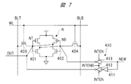
図7に示すように、スピンの値を記憶するメモリセルNは、SRAMと同様に、クロスカップル接続された一対のCMOSインバータ401,402と、この一対のCMOSインバータの記憶ノードNT,NBにそれぞれ接続されたパスゲートトランジスタ403,404から構成される。一対のCMOSインバータ401,402は、互いに、ゲートは出力に接続され、出力はゲートに接続されている。この一対のCMOSインバータ401,402の各ゲートが記憶ノードNT,NBとなる。パスゲートトランジスタ403,404は、それぞれ、記憶ノードNT,NBとビット線BLT,BLBとの間に接続され、ゲートがワード線WLに接続されている。
As shown in FIG. 7, the memory cell N that stores the spin value is connected to a pair of
このメモリセルNにスピンの値を書き込む書き込み回路410は、スピンの値NEWを入力として、インバータ411およびクロックドインバータ412の直列回路と、クロックドインバータ413とが並列に接続されて構成される。この並列接続において、インバータ411およびクロックドインバータ412の直列回路から記憶ノードNTに接続され、クロックドインバータ413から記憶ノードNBに接続されている。クロックドインバータ412,413は、相互作用の実行を許可または非許可にする相補の相互作用信号(相互作用信号INTENと、これを反転した反転相互作用信号INTENB)により制御される。この書き込み回路410は、相互作用計算回路340に含まれる。
The
この図7に示す回路構成では、クロスカップル接続された一対のCMOSインバータ401,402により、記憶ノードNTおよびNBにおいて1ビットのデータが保持される。スピンのメモリセルNのデータをチップの外部から読み出し、書き込みを行う際には、ワード線WLとビット線BLTおよびBLBが用いられる。
In the circuit configuration shown in FIG. 7, 1-bit data is held in storage nodes NT and NB by a pair of
一方、スピンユニット300において、相互作用が計算された場合には、スピンユニット300内でデータが書き込まれる。新しいデータはNEWから入力され、それを相互作用信号INTENおよびINTENBにより制御する。詳細な動作波形を図8に示す。相互作用期間は、相互作用信号INTENがハイ、反転相互作用信号INTENBがロウの期間である。この相互作用計算中は、NEWの値がそのまま記憶ノードNTおよびNBに伝えられる。よって、相互作用期間に、NEWの値が変化し、スピンの値(メモリセルN)も変化する。また、相互作用をさせない相互作用不可期間では、相互作用信号INTENをディセーブル(ロウ)にする。
On the other hand, when the interaction is calculated in the
また、メモリセルNに書き込まれたスピンの値は、メモリセルNの記憶ノードNTから、隣接するスピンユニットへ出力(OUT)される。 The spin value written in the memory cell N is output (OUT) from the storage node NT of the memory cell N to the adjacent spin unit.
<10.相互作用計算回路の回路構成および回路動作>
図9〜図11は、相互作用計算回路の回路構成および回路動作の一例を説明するための図である。すなわち、図9および図10の相互作用計算回路は、上述した図6に示したスピンユニット300内の、排他的論理和回路310、スイッチ回路320、および多数決論理回路330を含めた相互作用計算回路340の論理回路を実現するための回路構成を示している。図9は、多数決論理の電流を足し合わせる回路を示し、図10は図9で足し合わせた電流を比較する回路を示している。また、図11は、図9および図10の相互作用計算回路340の動作波形を示している。
<10. Circuit configuration and circuit operation of interaction calculation circuit>
9 to 11 are diagrams for explaining an example of the circuit configuration and circuit operation of the interaction calculation circuit. That is, the interaction calculation circuit of FIGS. 9 and 10 includes an interaction calculation circuit including the exclusive OR
図9では、+1(または、0、上)のスピンの電流を足し合わせる+1計算回路510と、−1(または、1、下)のスピンの電流を足し合わせる−1計算回路530とに分けて、多数決論理の電流を足し合わせる部分の回路構成を示している。図9において、+1計算回路510は上側に図示し、−1計算回路530は下側に図示している。
In FIG. 9, a +1
+1計算回路510は、5つのNMOSトランジスタ511,512,513,514,515からなる並列接続の5組のブロックと、各ブロックを電源電位に接続するPMOSトランジスタ521とから構成される。PMOSトランジスタ521は、図11に示す相互作用信号INTENによりゲート制御され、相互作用信号INTENの電圧レベルがハイの期間にはオフし、逆に、ロウの期間にはオンする。
The +1
5組のブロックは、外部磁場係数ISxと、相互作用係数IUx(上側のスピン)、ILx(左側のスピン)、IRx(右側のスピン)、IDx(下側のスピン)に対応する各ブロックである。相互作用係数IUxに対応するブロックに着目すると、このブロックは、NUT、NUB、IU1T、IU1B、IU0でそれぞれゲート制御されるNMOSトランジスタ511,512,513,514,515から構成される。NMOSトランジスタ511,512,513,514,515は、それぞれ、対応するNUT、NUB、IU1T、IU1B、IU0の電圧レベルがハイの時にはオンし、逆に、ロウの時にはオフする。NMOSトランジスタ511と513とが直列に接続され、また、NMOSトランジスタ512と514とが直列に接続されている。この直列に接続されたNMOSトランジスタ511,513とNMOSトランジスタ512,514とが並列に接続されている。
The five sets of blocks are blocks corresponding to the external magnetic field coefficient ISx, the interaction coefficient IUx (upper spin), ILx (left spin), IRx (right spin), and IDx (lower spin). . Focusing on the block corresponding to the interaction coefficient IUx, this block is composed of
この並列接続において、NMOSトランジスタ511,512は、共通線CTに接続されている。この共通線CTは、PMOSトランジスタ521を介して電源電位に接続されている。一方、並列接続において、NMOSトランジスタ513,514は共通にNMOSトランジスタ515に接続されている。このNMOSトランジスタ515は、電流比較線CS1に接続される。この電流比較線CS1から、+1計算回路510の足し合わせた電流I1が取り出される。この相互作用係数IUxに対応するブロックでは、電流が流れるパスを2つ構成している。
In this parallel connection, the
他の相互作用係数ILx,IRx,IDxに対応するブロックにおいても、同様である。ILxに対応するブロックは、NLT、NLB、IL1T、IL1B、IL0でそれぞれゲート制御されるNMOSトランジスタ511,512,513,514,515から構成される。IRxに対応するブロックは、NRT、NRB、IR1T、IR1B、IR0でそれぞれゲート制御されるNMOSトランジスタ511,512,513,514,515から構成される。IDxに対応するブロックは、NDT、NDB、ID1T、ID1B、ID0でそれぞれゲート制御されるNMOSトランジスタ511,512,513,514,515から構成される。
The same applies to blocks corresponding to other interaction coefficients ILx, IRx, and IDx. The block corresponding to ILx includes
また、外部磁場係数ISxに対応するブロックは、ハイ固定、ハイ固定、IS1T、IS1B、IS0でそれぞれゲート制御されるNMOSトランジスタ511,512,513,514,515から構成される。この外部磁場係数ISxは、隣接するスピンユニットからの入力がないので、NMOSトランジスタ511,512のゲートはハイに固定され、NMOSトランジスタ511,512はオン状態になっている。
The block corresponding to the external magnetic field coefficient ISx is composed of
−1計算回路530も同様に、5つのNMOSトランジスタ531,532,533,534,535からなる並列接続の5組のブロックと、各ブロックを電源電位に接続するPMOSトランジスタ541とから構成される。この−1計算回路530では、電流比較線CS2から足し合わせた電流I2が取り出される。ただし、−1計算回路530が、+1計算回路510と異なる点は、例えば、相互作用係数IUxに対応するブロックにおいて、IU1Tでゲート制御されるNMOSトランジスタ533とIU1Bでゲート制御されるNMOSトランジスタ534とが入れ替えて接続されている。すなわち、NMOSトランジスタ531と534とが直列に接続され、また、NMOSトランジスタ532と533とが直列に接続されている。他の相互作用係数ILx,IRx,IDxに対応するブロック、外部磁場係数ISxに対応するブロックにおいても、同様である。
Similarly, the -1
以上のように構成される+1計算回路510および−1計算回路530では、以下のような動作となる。ここでは、簡単のため、相互作用係数IUxに対応するブロックに着目し、NUから入力されたデータとIU0およびIU1に保持された相互作用係数を用いた計算を行う部分を説明する。
The +1
それぞれのNMOSトランジスタが接続されている共通線CTおよび共通線CBは、相互作用計算を行う前、つまり図11に示す相互作用信号INTENの電圧レベルがロウの期間に、ハイの電位にプリチャージされる。相互作用信号INTENはハイになると、相互作用の値の計算が開始される。 The common line CT and the common line CB to which the respective NMOS transistors are connected are precharged to a high potential before the interaction calculation is performed, that is, when the voltage level of the interaction signal INTEN shown in FIG. 11 is low. The When the interaction signal INTEN goes high, the calculation of the interaction value is started.
NUから入力されたデータは、NUTとNUBの相補の信号に分割される。つまり、NUTはNUの値、NUBはNUの反転した値となる。また、相互作用係数のIU1も相補の信号IU1TとIU1Bとなる。IU0は、その相互作用係数を0にするか1にするかを示しており、IU0が0の場合には相互作用係数の値の影響がなくなるため、IU0が入力されたNMOSトランジスタ515,535がオフとなり、電流が流れず計算結果に影響を与えない。IU0が1の場合には、IU0が入力されたNMOSトランジスタ515,535がオンとなり、NUおよびIU1が関連する電流パスがオンとなる。
Data input from the NU is divided into complementary signals of NUT and NUB. That is, NUT is a value of NU, and NUB is a value obtained by inverting NU. The interaction coefficient IU1 is also complementary signals IU1T and IU1B. IU0 indicates whether the interaction coefficient is set to 0 or 1. When IU0 is 0, the influence of the value of the interaction coefficient is eliminated, so that the
NUとIU1の値が等しい場合には、NUTとIU1Tが入力されたNMOSトランジスタ511,513が直列接続されたパス、またはNUBとIU1Bが入力されたNMOSトランジスタ512,514が直列接続されたパスを通して電流が流れ、電流比較線CS1から取り出す電流I1が足し合わされる。逆に、NUとIU1の値が異なる場合には、NUTとIU1Bが入力されたNMOSトランジスタ531,534が直列接続されたパス、またはNUBとIU1Tが入力されたNMOSトランジスタ532,533が直列接続されたパスを通して電流が流れ、電流比較線CS2から取り出す電流I2が足し合わされる。
When the values of NU and IU1 are equal, the
このことは、他の相互作用係数ILx,IRx,IDxに対応するブロックにおいても、同様である。それぞれ、NL、NR、NDから入力されたデータとIL0、IR0、ID0およびIL1、IR1、ID1に保持された相互作用係数を用いた計算を行う。 The same applies to blocks corresponding to other interaction coefficients ILx, IRx, and IDx. Calculations are performed using data input from NL, NR, and ND and interaction coefficients held in IL0, IR0, ID0, and IL1, IR1, and ID1, respectively.
つまり、入力されたデータと相互作用係数の値が等しい係数に関しては電流比較線CS1から取り出す電流I1が足し合わされ、入力されたデータと相互作用係数の値が異なる係数に関しては電流比較線CS2から取り出す電流I2が足し合わされる。つまり、図6に示した排他的論理和の値が1になる係数に関しては電流比較線CS1から取り出す電流I1が足し合わされ、0になる係数に関しては電流比較線CS2から取り出す電流I2が足し合わされる。よって、電流比較線CS1から取り出す電流I1と電流比較線CS2から取り出す電流I2とを比較すれば、どちらが多いかの多数決を計算することができる。 In other words, the current I1 taken out from the current comparison line CS1 is added for the coefficient having the same interaction coefficient value as the input data, and the coefficient having the interaction coefficient value different from the input data is taken out from the current comparison line CS2. The current I2 is added. That is, the current I1 extracted from the current comparison line CS1 is added for the coefficient with the exclusive OR value of 1 shown in FIG. 6, and the current I2 extracted from the current comparison line CS2 is added for the coefficient of 0. . Therefore, if the current I1 taken out from the current comparison line CS1 and the current I2 taken out from the current comparison line CS2 are compared, the majority of which is more can be calculated.
上述した電流比較線CS1から取り出す電流I1と電流比較線CS2から取り出す電流I2とを比較する回路が、図10である。図10では、電流I1と電流I2とを比較する電流比較回路の回路構成を示している。電流比較回路550は、MOSトランジスタによるカレントミラー回路の組み合わせからなり、電流I1のカレントミラー回路と、電流I2のカレントミラー回路との2組から構成される。この電流比較回路550は、アナログ的な動作により、クロック同期は不要となっている。
FIG. 10 shows a circuit for comparing the current I1 extracted from the current comparison line CS1 and the current I2 extracted from the current comparison line CS2. FIG. 10 shows a circuit configuration of a current comparison circuit that compares the currents I1 and I2. The
電流I1のカレントミラー回路は、1つのPMOSトランジスタ551と、ゲート同士が接続された2つのNMOSトランジスタ552,553から構成される。電流I2のカレントミラー回路も、同様に、1つのPMOSトランジスタ556と、ゲート同士が接続された2つのNMOSトランジスタ557,558から構成される。
The current mirror circuit for the current I1 includes one
電流I1のカレントミラー回路において、PMOSトランジスタ551は、ソースが電源電位VDDに接続され、ドレインがNMOSトランジスタ553のドレインに接続されている。NMOSトランジスタ553は、ドレインがPMOSトランジスタ551のドレインに接続され、ソースが接地電位に接続され、ゲートがNMOSトランジスタ552のゲートに接続されている。NMOSトランジスタ552は、ドレインがゲートに接続されると共にNMOSトランジスタ553のゲートに接続され、ソースが接地電位に接続されている。
In the current mirror circuit of the current I1, the
電流I2のカレントミラー回路においても、同様の接続構成になっている。さらに、電流I1のカレントミラー回路におけるPMOSトランジスタ551のゲートと電流I2のカレントミラー回路におけるPMOSトランジスタ556のゲートとが接続されている。また、電流I1のカレントミラー回路におけるPMOSトランジスタ551のゲートとドレインとの間も接続されている。
The current I2 current mirror circuit has a similar connection configuration. Further, the gate of the
以上のような接続構成からなる電流比較回路550において、電流I1のカレントミラー回路におけるNMOSトランジスタ552のドレインに、+1計算回路510の電流比較線CS1から取り出した電流I1が供給される。また、電流I2のカレントミラー回路におけるNMOSトランジスタ557のドレインに、−1計算回路530の電流比較線CS2から取り出した電流I2が供給される。そして、この電流比較回路550の出力NEWは、電流I2のカレントミラー回路におけるPMOSトランジスタ556のドレインとNMOSトランジスタ558のドレインとの接続ノードから取り出される。
In the
この電流比較回路550においては、電流I1のカレントミラー回路におけるNMOSトランジスタ552のドレインに供給された電流I1は、NMOSトランジスタ553のドレインにも同じ電流I1が流れ、さらに、PMOSトランジスタ556のドレインにも同じ電流I1が流れる。また、電流I2のカレントミラー回路におけるNMOSトランジスタ557のドレインに供給された電流I2は、NMOSトランジスタ558のドレインにも同じ電流I2が流れる。そして、PMOSトランジスタ556のドレインに流れる電流I1とNMOSトランジスタ558のドレインに流れる電流I2とが比較される。この比較の結果、図11に示すように、電流I1が大きい場合、つまり入力されたデータと係数の排他的論理和の結果が1になる係数が多い場合にはスピンの次状態の値NEWとして1が出力され、電流I2が大きい場合、つまり入力されたデータと係数の排他的論理和の結果が0になる係数が多い場合にはスピンの次状態の値NEWとして0が出力される。
In this
以上の動作は、相互作用信号INTENの電圧レベルがハイとなる期間に実行される。このように相互作用信号INTENがハイの期間は、常に電流が評価されて出力NEWが変化する。この期間は、相互作用期間である。この相互作用期間では、+1(または、0、上)または−1(または、1、下)の多い方をスピンの次状態として決定することができる。また、相互作用信号INTENがロウの期間は電流がオフ(0)になる。この期間は、相互作用不可期間である。 The above operation is executed during a period when the voltage level of the interaction signal INTEN is high. Thus, during the period when the interaction signal INTEN is high, the current is always evaluated and the output NEW changes. This period is an interaction period. In this interaction period, the greater of +1 (or 0, up) or -1 (or 1, down) can be determined as the next state of spin. Further, the current is turned off (0) while the interaction signal INTEN is low. This period is an interaction impossible period.
なお、図9に示した多数決論理の電流を足し合わせる回路、図10に示した足し合わせた電流を比較する回路は、回路構成は種々の変更が可能である。例えば、図9の変形例として、各ブロックの接地電位側をNMOSトランジスタで接地して、電源電位側の電流を足し合わせる構成とすることができる。この構成の場合に、図10の回路構成は、PMOSトランジスタとNMOSトランジスタとを逆にした回路構成となる。すなわち、2組のカレントミラー回路において、それぞれ、ゲート同士が接続された2つのPMOSトランジスタが電源電位に接続され、NMOSトランジスタが接地電位に接続されて構成される。この構成において、2組のカレントミラー回路のPMOSトランジスタから各電流比較線に接続され、互いの電流比較線の電流の大きさが比較できる回路構成となる。 The circuit configuration for adding the majority logic currents shown in FIG. 9 and the circuit for comparing the added currents shown in FIG. 10 can be variously modified. For example, as a modification of FIG. 9, the ground potential side of each block can be grounded with an NMOS transistor, and the current on the power supply potential side can be added. In the case of this configuration, the circuit configuration of FIG. 10 is a circuit configuration in which the PMOS transistor and the NMOS transistor are reversed. That is, each of the two sets of current mirror circuits is configured such that two PMOS transistors whose gates are connected to each other are connected to a power supply potential, and an NMOS transistor is connected to a ground potential. In this configuration, the current comparison lines are connected to the current comparison lines from the PMOS transistors of the two sets of current mirror circuits, and the currents of the current comparison lines can be compared.
<11.イジングチップの相互作用動作>
図12〜図14は、イジングチップ100の相互作用動作の一例を説明するための図である。図12は、スピンユニット300の配置において、スピンの値の更新を一部に限る場合を示している。図13は、イネーブル信号とアドレス信号を使ってスピンユニット300内で相補の相互作用信号を作る回路を示している。図14は、図13の回路動作の動作波形を示している。
<11. Ising chip interaction>
12-14 is a figure for demonstrating an example of interaction operation | movement of the Ising chip |
このイジングチップ100の相互作用動作は、イジングチップ100を組み込んだ情報処理装置200において、イジングチップ100をCPU210が制御して基底状態探索における相互作用動作が実行される。
The interaction operation of the
相互作用動作の開始に先立って、初期設定として、対象問題を表現するイジングモデルについて、イジングチップ100の各スピンユニット300内のメモリセルに、スピンの値、相互作用係数、および、外部磁場係数を入力する。
Prior to the start of the interaction operation, as an initial setting, for the Ising model expressing the target problem, the spin value, the interaction coefficient, and the external magnetic field coefficient are stored in the memory cells in each
初期設定の完了後、相互作用動作が開始になると、各スピンユニット300の相互作用計算を実行する。この相互作用計算では、相互作用アドレス線180を介してアドレスをイジングチップ100に入力し、相互作用イネーブル線181を介して相互作用信号を生成してイジングチップ100内で相互作用を起こさせる。また、スピン用電源線141に供給される電圧をスケジューリングに沿って制御する。
When the interaction operation starts after completion of the initial setting, the interaction calculation of each
この場合に、全てのスピンを同時に更新しようとすると、あるスピンを更新するときに、隣接するスピンを見て、隣接するスピンとの間でエネルギーを最小化するようにスピンを更新するので、それと同時に隣接するスピンの値を更新すると、両方の更新が重複してしまい、エネルギーを最小化できずに振動してしまう。そこで、本実施の形態では、隣接するスピンを同時に更新しないように、スピンアレイ110内のスピンユニット300をグループ分けしている。
In this case, if you try to update all the spins at the same time, when you update a certain spin, you see the adjacent spins and update the spins to minimize the energy between adjacent spins. If the values of adjacent spins are updated at the same time, both updates are duplicated, and the energy cannot be minimized and vibrates. Therefore, in this embodiment, the
図12では、複数のスピンユニット300として、行方向に6個、列方向に4個を2次元格子状に配置している例を図示している。各スピンユニット300を区別するために、説明上便宜的に、座標(Nxyz、x=0,1,2、y=0,1,2,3、z=0,1)を付与している。このように2次元格子状に配置された複数のスピンユニット300は、外部から入力されるイネーブル信号IENとアドレス信号IAD[0],[1],[2],[3]により相互作用が制御される。
FIG. 12 illustrates an example in which six
各スピンユニット300では、図13に示すように、外部から入力されたイネーブル信号IENとアドレス信号IADとを使って、相互作用の実行を許可または非許可にする相互作用信号INTEN,INTENBを作る相互作用信号生成回路600を有している。この相互作用信号生成回路600は、NAND回路601と、インバータ602とから構成される。NAND回路601は、イネーブル信号IENとアドレス信号IADとを入力として、論理積の否定演算を行い、その演算結果を相互作用信号INTENBとして出力する。インバータ602は、NAND回路601の出力を反転して、相互作用信号INTENとして出力する。
In each of the
この相互作用信号生成回路600の動作波形は、図14のようになる。イネーブル信号IENがハイの期間は、相互作用が起きる相互作用期間である。一方、イネーブル信号IENがロウの期間は、相互作用が起こらず、メモリセルへのアクセスが実行されるメモリアクセス期間である。
The operation waveform of the interaction
相互作用期間において、イネーブル信号IENがハイの期間にアドレス信号IADが入ると、対応する相互作用信号INTENがハイとなる。この時に、アドレス信号IADが入ったスピンユニット300において、スピンの値の更新が行われる。例えば、図12において、アドレス信号IAD[0]の例では、このアドレス信号IAD[0]が入ったスピンユニットN000,N200,N110,N020,N220,N130において同時に、スピンの値の更新が行われる。この場合に、例えばスピンユニットN110に着目すると、このスピンユニットN110の上側のスピンユニットN100と左側のスピンユニットN011と右側のスピンユニットN111と下側のスピンユニットN120は更新が行われない。この結果、隣接するスピンユニットで同時に更新が起こらない。
In the interaction period, when the address signal IAD is input while the enable signal IEN is high, the corresponding interaction signal INTEN becomes high. At this time, the spin value is updated in the
他のアドレス信号IAD[1]〜[3]の例でも同様に、アドレス信号IAD[1]が入ったスピンユニットN001,N201,N111,N021,N221,N131が同時に更新され、アドレス信号IAD[2]が入ったスピンユニットN100,N010,N210,N120,N030,N230が同時に更新され、アドレス信号IAD[3]が入ったスピンユニットN101,N011,N211,N121,N031,N231が同時に更新される。このように、スピンの値の更新を一部に限り、隣接するスピンユニットで同時に更新が起こらないようにしている。 Similarly, in the examples of the other address signals IAD [1] to [3], the spin units N001, N201, N111, N021, N221, and N131 containing the address signal IAD [1] are simultaneously updated, and the address signal IAD [2 ] Are simultaneously updated, and spin units N101, N011, N211, N121, N031, and N231 containing address signal IAD [3] are simultaneously updated. In this way, the update of the spin value is limited to a part, so that the adjacent spin units do not update simultaneously.
そして、全てのスピンユニットの相互作用計算を所定の時間繰り返した後、相互作用動作が終了となる。所定の時間は、例えば対象問題に応じて最適な時間を設定する。なお、イネーブル信号のON/OFFを何回実行するかも設定する。この相互作用動作が終了となると、イジングチップ100から相互作用計算結果であるスピンの値を読み出すことで、対象問題を表現するイジングモデルの答えを得ることができる。
Then, after the interaction calculation of all the spin units is repeated for a predetermined time, the interaction operation is completed. As the predetermined time, for example, an optimal time is set according to the target problem. It is also set how many times the enable signal is turned ON / OFF. When this interaction operation ends, the Ising model answer expressing the target problem can be obtained by reading the spin value as the interaction calculation result from the
<12.効果>
以上説明した本実施の形態によれば、スピンユニット300内の相互作用計算回路340はアナログ回路を含むことで、イジングモデルの基底状態を求めるイジングチップ100において、クロックに非同期で相互作用計算を実行可能にする技術を提供することができる。より詳細には、以下の通りである。
<12. Effect>
According to the present embodiment described above, the
(1)隣接するスピンの値とこれに対応する相互作用係数との積、および外部磁場係数において、2値の多数決論理によってスピンの次状態を決定する相互作用計算回路340は、アナログ回路を含む。これにより、アナログ的な動作によりクロック同期を不要にして、相互作用計算を実行することができる。
(1) The
(2)相互作用計算回路340は、相互作用の実行を許可または非許可にする相互作用信号INTEN,INTENBで制御することができる。これにより、クロック同期が不要で、相互作用の実行が許可の期間は相互作用を常に評価することができる。
(2) The
(3)相互作用計算回路340は、+1計算回路510と−1計算回路530とを含む論理回路と、+1計算回路510と−1計算回路530との足し合わせ電流を比較する電流比較回路550とを有する。これにより、+1計算回路510は、並列接続の複数の電流パスからなる構成において、+1のスピンの電流を足し合わせることができる。かつ、−1計算回路530は、並列接続の複数の電流パスからなる構成において、−1のスピンの電流を足し合わせることができる。そして、電流比較回路550は、カレントミラー回路の組み合わせからなる構成において、+1計算回路510の結果が現れる電流比較線CS1の電流と−1計算回路530の結果が現れる電流比較線CS2の電流とを比較して、大きい方の電流に対応する値をスピンの次状態を決定する値として出力することができる。
(3) The
(4)相互作用計算回路340は、相互作用信号INTENがハイの相互作用期間に、+1計算回路510および−1計算回路530における電流の足し合わせを行い、電流比較回路550におけるスピンの次状態を決定する値を変化させることができる。相互作用信号INTENがロウの相互作用不可期間に、+1計算回路510および−1計算回路530における電流をオフにすることができる。
(4) The
(5)相互作用計算回路340は、メモリセルNへの書き込み回路410を含み、この書き込み回路410を相互作用信号INTEN,INTENBで制御することができる。これにより、クロック同期を不要にして、相互作用計算で決定した次状態の値をメモリセルNに書き込むことができる。
(5) The
(6)スピンユニット300は、相互作用信号生成回路600を含み、この相互作用信号生成回路600で生成した相互作用信号INTEN,INTENBに基づいて制御することができる。これにより、スピンの値を更新するスピンユニット300を制限することができる。
(6) The
(7)スピンユニット300は、相互作用信号INTEN,INTENBに基づいて隣接するスピンユニット300の同時更新を禁止することができる。
(7) The
(8)相互作用信号生成回路600は、論理回路を含むことで、アドレス信号IADを使用して相互作用信号INTEN,INTENBを生成することができる。
(8) The interaction
(9)情報処理装置200において、イジングチップ100の制御プログラムは、スピンアレイ110内のスピンユニット300へ、スピンの値、相互作用係数、および外部磁場係数を書き込む。そして、スピンユニット300の基底状態探索処理を所定の回数繰り返して実行することで、基底状態に達したスピンユニット300のスピンの値を読み出して対象問題の解を得ることができる。
(9) In the
以上、本発明者によってなされた発明をその実施の形態に基づき具体的に説明したが、本発明は前記実施の形態に限定されるものではなく、その要旨を逸脱しない範囲で種々変更可能であることは言うまでもない。 As mentioned above, the invention made by the present inventor has been specifically described based on the embodiment. However, the invention is not limited to the embodiment, and various modifications can be made without departing from the scope of the invention. Needless to say.
例えば、上記した実施の形態は、本発明を分かり易く説明するために詳細に説明したものであり、必ずしも説明した全ての構成を備えるものに限定されるものではない。また、実施の形態の構成の一部について、他の構成の追加・削除・置換をすることが可能である。 For example, the above-described embodiment has been described in detail for easy understanding of the present invention, and is not necessarily limited to one having all the configurations described. In addition, it is possible to add, delete, and replace other configurations for a part of the configuration of the embodiment.
また、上記した実施の形態では、物理学の世界で代表的なイジングモデルを例にあげて説明したが、本発明はこれに限定されるものではなく、種々の物理現象や社会現象を表現することができる相互作用モデル全般に適用できるものである。 In the above-described embodiment, the Ising model typical in the physics world has been described as an example. However, the present invention is not limited to this, and expresses various physical and social phenomena. It can be applied to all possible interaction models.
100,100−1,100−2 イジングチップ
110 スピンアレイ
120 I/Oドライバ
130 I/Oアドレスデコーダ
140 相互作用アドレスデコーダ
141 スピン用電源線
142 通常電源線
150 SRAM互換インタフェース
160 相互作用制御インタフェース
180 相互作用アドレス線
181 相互作用イネーブル線
190 アドレスバス(SRAM互換インタフェース)
191 データバス(SRAM互換インタフェース)
192 I/Oイネーブル線(SRAM互換インタフェース)
193 R/W制御線(SRAM互換インタフェース)
200 情報処理装置
210 CPU
220 RAM
230 システムバス
240 NIC
250 イジングチップコントローラ
260 HDD
290 装置間ネットワーク
300 スピンユニット
310 排他的論理和回路
320 スイッチ回路
330 多数決論理回路
340 相互作用計算回路
410 書き込み回路
510 +1計算回路
530 −1計算回路
550 電流比較回路
600 相互作用信号生成回路
N,IS0,IS1,IU0,IU1,IL0,IL1,IR0,IR1,ID0,ID1 メモリセル
100, 100-1, 100-2
191 Data bus (SRAM compatible interface)
192 I / O enable line (SRAM compatible interface)
193 R / W control line (SRAM compatible interface)
200
220 RAM
230
250
290
Claims (15)
前記相互作用計算回路は、相互作用の実行を許可または非許可にする相互作用信号で制御される、半導体装置。 The semiconductor device according to claim 1,
The interaction calculation circuit is a semiconductor device controlled by an interaction signal that permits or disallows the execution of the interaction.
前記相互作用計算回路は、
前記接続されたノードの状態を示す値及び前記相互作用係数に基づいて、第1の値と第2の値との電流を足し合わせる論理回路と、
前記論理回路の結果に基づいて、前記足し合わせ電流を比較して前記1つのノードの次状態を示す値として前記第1の値または前記第2の値を出力する比較回路と、
を含む、半導体装置。 The semiconductor device according to claim 2,
The interaction calculation circuit is:
A logic circuit that adds the currents of the first value and the second value based on the value indicating the state of the connected node and the interaction coefficient;
A comparison circuit that compares the sum current and outputs the first value or the second value as a value indicating a next state of the one node based on a result of the logic circuit;
Including a semiconductor device.
前記論理回路は、前記接続されたノードの状態を示す値及び前記相互作用係数に基づいてそれぞれゲート制御される複数のMOSトランジスタによる並列接続の複数の電流パスからなり、前記第1の値の電流を足し合わせる第1計算回路と、前記接続されたノードの状態を示す値及び前記相互作用係数に基づいてそれぞれゲート制御される複数のMOSトランジスタによる並列接続の複数の電流パスからなり、前記第2の値の電流を足し合わせる第2計算回路と、を含み、
前記比較回路は、MOSトランジスタによるカレントミラー回路の組み合わせからなり、前記第1計算回路の結果が現れる第1電流比較線の電流と前記第2計算回路の結果が現れる第2電流比較線の電流とを比較して、大きい方の電流に対応する前記第1の値または前記第2の値を前記1つのノードの次状態を示す値として出力する、半導体装置。 The semiconductor device according to claim 3.
The logic circuit includes a plurality of current paths connected in parallel by a plurality of MOS transistors gate-controlled based on the value indicating the state of the connected node and the interaction coefficient, and the current of the first value And a plurality of current paths connected in parallel by a plurality of MOS transistors gate-controlled based on the value indicating the state of the connected node and the interaction coefficient, respectively, A second calculation circuit for adding currents of the values of
The comparison circuit comprises a combination of current mirror circuits of MOS transistors, and the current of the first current comparison line where the result of the first calculation circuit appears and the current of the second current comparison line where the result of the second calculation circuit appears. And outputting the first value or the second value corresponding to the larger current as a value indicating the next state of the one node.
前記相互作用計算回路は、
前記相互作用信号が相互作用の実行を許可する期間に、前記第1計算回路および前記第2計算回路における電流の足し合わせが行われ、前記比較回路における前記1つのノードの次状態を示す値が変化し、
前記相互作用信号が相互作用の実行を非許可にする期間に、前記第1計算回路および前記第2計算回路における電流がオフになる、半導体装置。 The semiconductor device according to claim 4,
The interaction calculation circuit is:
During the period when the interaction signal permits execution of the interaction, the currents in the first calculation circuit and the second calculation circuit are added, and a value indicating the next state of the one node in the comparison circuit is obtained. Change,
The semiconductor device, wherein the current in the first calculation circuit and the second calculation circuit is turned off during a period in which the interaction signal does not permit execution of the interaction.
前記相互作用計算回路は、前記比較回路から出力する前記第1の値または前記第2の値を前記第1メモリセルに書き込む書き込み回路を含み、前記書き込み回路は、前記相互作用信号で制御される、半導体装置。 The semiconductor device according to claim 3.
The interaction calculation circuit includes a write circuit that writes the first value or the second value output from the comparison circuit into the first memory cell, and the write circuit is controlled by the interaction signal. , Semiconductor devices.
前記複数のユニットのそれぞれは、前記相互作用信号を生成する生成回路を含み、前記生成回路で生成した前記相互作用信号に基づいて、前記ノードの状態を示す値を更新するユニットが制限される、半導体装置。 The semiconductor device according to claim 2,
Each of the plurality of units includes a generation circuit that generates the interaction signal, and a unit that updates a value indicating the state of the node is limited based on the interaction signal generated by the generation circuit. Semiconductor device.
前記複数のユニットのそれぞれは、前記相互作用信号に基づいて、隣接するユニットの同時更新が禁止される、半導体装置。 The semiconductor device according to claim 7,
Each of the plurality of units is a semiconductor device in which simultaneous updating of adjacent units is prohibited based on the interaction signal.
前記生成回路は、アドレス信号を使用して前記相互作用信号を生成する論理回路を含む、半導体装置。 The semiconductor device according to claim 8,
The generation circuit includes a logic circuit that generates the interaction signal using an address signal.
前記半導体装置は、
相互作用モデルの1つのノードの状態を示す値を記憶する第1メモリセルと、前記1つのノードに接続されたノードからの相互作用を示す相互作用係数を記憶する第2メモリセルと、前記接続されたノードの状態を示す値及び前記相互作用係数により決定される電流に基づいて、前記1つのノードの次状態を示す値を決定する相互作用計算回路と、をそれぞれ含む複数のユニットと、
前記複数のユニットのメモリセルをリード/ライトするI/Oインタフェースと、
前記複数のユニットに対して、相互作用を許可する信号を供給する相互作用制御インタフェースと、を有し、
前記CPU上で実行される前記半導体装置の制御プログラムは、
対象問題を表現する前記相互作用モデルの各ノードを割り当てた前記半導体装置上の前記複数のユニットへ、前記ノードの状態を示す値、および前記相互作用係数を書き込み、
前記複数のユニットの基底状態探索処理を所定の時間繰り返して実行し、
基底状態に達した前記複数のユニットのノードの状態を示す値を読み出して前記対象問題の解を得る、情報処理装置。 An information processing apparatus in which a CPU, a RAM, an HDD, and a semiconductor device operable as an accelerator are connected via a system bus,
The semiconductor device includes:
A first memory cell storing a value indicating a state of one node of the interaction model; a second memory cell storing an interaction coefficient indicating an interaction from a node connected to the one node; and the connection A plurality of units each including an interaction calculation circuit that determines a value indicating a next state of the one node based on a value indicating a state of the node and a current determined by the interaction coefficient;
An I / O interface for reading / writing the memory cells of the plurality of units;
An interaction control interface for supplying a signal allowing the interaction to the plurality of units;
The control program for the semiconductor device executed on the CPU is:
Write a value indicating the state of the node and the interaction coefficient to the plurality of units on the semiconductor device to which each node of the interaction model expressing the target problem is assigned,
The ground state search process of the plurality of units is repeatedly executed for a predetermined time,
An information processing apparatus that obtains a solution to the target problem by reading a value indicating a state of a node of the plurality of units that has reached a ground state.
前記複数のユニットの基底状態探索処理は、相互作用の実行を許可または非許可にする相互作用信号で制御する、情報処理装置。 The information processing apparatus according to claim 10,
The information processing apparatus that controls the ground state search processing of the plurality of units by an interaction signal that permits or disallows the execution of the interaction.
前記複数のユニットの基底状態探索処理は、
前記相互作用信号が相互作用の実行を許可する期間に、前記相互作用計算回路における電流の足し合わせを行い、前記1つのノードの状態を示す値を変化させ、
前記相互作用信号が相互作用の実行を非許可にする期間に、前記相互作用計算回路における電流をオフにする、情報処理装置。 The information processing apparatus according to claim 11,
The ground state search process of the plurality of units is:
During the period in which the interaction signal permits execution of an interaction, the currents in the interaction calculation circuit are added, and the value indicating the state of the one node is changed,
An information processing apparatus that turns off the current in the interaction calculation circuit during a period in which the interaction signal does not permit execution of an interaction.
前記複数のユニットの基底状態探索処理は、前記相互作用信号に基づいて、前記相互作用計算回路で決定されたノードの次状態を示す値を前記第1メモリセルに書き込む、情報処理装置。 The information processing apparatus according to claim 12,
The ground state search processing of the plurality of units is an information processing apparatus that writes a value indicating a next state of a node determined by the interaction calculation circuit to the first memory cell based on the interaction signal.
前記複数のユニットの基底状態探索処理は、前記相互作用信号に基づいて、前記ノードの状態を示す値を更新するユニットを制限する、情報処理装置。 The information processing apparatus according to claim 11,
The ground state search processing of the plurality of units is an information processing apparatus that restricts units that update a value indicating the state of the node based on the interaction signal.
前記複数のユニットの基底状態探索処理は、前記相互作用信号に基づいて、隣接するユニットの同時更新を禁止する、情報処理装置。 The information processing apparatus according to claim 14,
The ground state search processing of the plurality of units is an information processing apparatus that prohibits simultaneous updating of adjacent units based on the interaction signal.
Priority Applications (2)
| Application Number | Priority Date | Filing Date | Title |
|---|---|---|---|
| JP2014176385A JP5903471B2 (en) | 2014-08-29 | 2014-08-29 | Semiconductor device and information processing apparatus |
| US14/642,266 US9588911B2 (en) | 2014-08-29 | 2015-03-09 | Semiconductor system for implementing an ising model of interaction |
Applications Claiming Priority (1)
| Application Number | Priority Date | Filing Date | Title |
|---|---|---|---|
| JP2014176385A JP5903471B2 (en) | 2014-08-29 | 2014-08-29 | Semiconductor device and information processing apparatus |
Publications (2)
| Publication Number | Publication Date |
|---|---|
| JP2016052012A true JP2016052012A (en) | 2016-04-11 |
| JP5903471B2 JP5903471B2 (en) | 2016-04-13 |
Family
ID=55403242
Family Applications (1)
| Application Number | Title | Priority Date | Filing Date |
|---|---|---|---|
| JP2014176385A Expired - Fee Related JP5903471B2 (en) | 2014-08-29 | 2014-08-29 | Semiconductor device and information processing apparatus |
Country Status (2)
| Country | Link |
|---|---|
| US (1) | US9588911B2 (en) |
| JP (1) | JP5903471B2 (en) |
Families Citing this family (2)
| Publication number | Priority date | Publication date | Assignee | Title |
|---|---|---|---|---|
| JP6021864B2 (en) * | 2014-08-29 | 2016-11-09 | 株式会社日立製作所 | Semiconductor device and information processing apparatus |
| JP6914872B2 (en) * | 2018-02-27 | 2021-08-04 | 株式会社日立製作所 | Information processing equipment and semiconductor integrated circuit equipment |
Citations (4)
| Publication number | Priority date | Publication date | Assignee | Title |
|---|---|---|---|---|
| JPS6427315A (en) * | 1987-04-09 | 1989-01-30 | Nec Corp | Logic circuit |
| JPH02276310A (en) * | 1989-04-18 | 1990-11-13 | Res Dev Corp Of Japan | Logic circuit |
| JPH04156108A (en) * | 1990-10-19 | 1992-05-28 | Fujitsu Ltd | Majority decision circuit |
| JP2009026181A (en) * | 2007-07-23 | 2009-02-05 | Ryukoku Univ | Neural network |
Family Cites Families (2)
| Publication number | Priority date | Publication date | Assignee | Title |
|---|---|---|---|---|
| US9411026B2 (en) | 2011-03-01 | 2016-08-09 | Inter-University Research Institute Corporation, Research Organization of Information and systems | Ising model quantum computation device and Ising model quantum computation method |
| EP2812737B1 (en) * | 2012-02-09 | 2018-04-11 | Saudi Arabian Oil Company | Multi-level solution of large-scale linear systems in simulation of porous media in giant reservoirs |
-
2014
- 2014-08-29 JP JP2014176385A patent/JP5903471B2/en not_active Expired - Fee Related
-
2015
- 2015-03-09 US US14/642,266 patent/US9588911B2/en active Active
Patent Citations (4)
| Publication number | Priority date | Publication date | Assignee | Title |
|---|---|---|---|---|
| JPS6427315A (en) * | 1987-04-09 | 1989-01-30 | Nec Corp | Logic circuit |
| JPH02276310A (en) * | 1989-04-18 | 1990-11-13 | Res Dev Corp Of Japan | Logic circuit |
| JPH04156108A (en) * | 1990-10-19 | 1992-05-28 | Fujitsu Ltd | Majority decision circuit |
| JP2009026181A (en) * | 2007-07-23 | 2009-02-05 | Ryukoku Univ | Neural network |
Also Published As
| Publication number | Publication date |
|---|---|
| US9588911B2 (en) | 2017-03-07 |
| US20160064080A1 (en) | 2016-03-03 |
| JP5903471B2 (en) | 2016-04-13 |
Similar Documents
| Publication | Publication Date | Title |
|---|---|---|
| JP5865456B1 (en) | Semiconductor device | |
| US9823882B2 (en) | Semiconductor device and information processing device | |
| JP5864684B1 (en) | Semiconductor device | |
| JP5901712B2 (en) | Semiconductor device and information processing apparatus | |
| JP5922203B2 (en) | Semiconductor device | |
| JP6177993B2 (en) | Semiconductor device and information processing apparatus | |
| JP6568222B2 (en) | Semiconductor system and calculation method | |
| US10366745B2 (en) | Semiconductor device and information processing device | |
| JP6295325B2 (en) | Semiconductor device and information processing system | |
| JP5894645B1 (en) | Semiconductor device and quality control method thereof | |
| JP5851570B1 (en) | Semiconductor device | |
| Hayashi et al. | Accelerator chip for ground-state searches of Ising model with asynchronous random pulse distribution | |
| JP2016051313A (en) | Semiconductor device, image segmentation method, and image processing device | |
| JPWO2017037903A1 (en) | Semiconductor system and calculation method | |
| JP5903471B2 (en) | Semiconductor device and information processing apparatus | |
| JP6207583B2 (en) | Semiconductor device and information processing method | |
| WO2017033263A1 (en) | Information processing system |
Legal Events
| Date | Code | Title | Description |
|---|---|---|---|
| A521 | Request for written amendment filed |
Free format text: JAPANESE INTERMEDIATE CODE: A523 Effective date: 20160210 |
|
| TRDD | Decision of grant or rejection written | ||
| A01 | Written decision to grant a patent or to grant a registration (utility model) |
Free format text: JAPANESE INTERMEDIATE CODE: A01 Effective date: 20160301 |
|
| A61 | First payment of annual fees (during grant procedure) |
Free format text: JAPANESE INTERMEDIATE CODE: A61 Effective date: 20160314 |
|
| R150 | Certificate of patent or registration of utility model |
Ref document number: 5903471 Country of ref document: JP Free format text: JAPANESE INTERMEDIATE CODE: R150 |
|
| LAPS | Cancellation because of no payment of annual fees |