JP2015526966A - Reconfigurable optical network - Google Patents
Reconfigurable optical network Download PDFInfo
- Publication number
- JP2015526966A JP2015526966A JP2015520377A JP2015520377A JP2015526966A JP 2015526966 A JP2015526966 A JP 2015526966A JP 2015520377 A JP2015520377 A JP 2015520377A JP 2015520377 A JP2015520377 A JP 2015520377A JP 2015526966 A JP2015526966 A JP 2015526966A
- Authority
- JP
- Japan
- Prior art keywords
- optical
- microcavity
- wavelength
- resonators
- output
- Prior art date
- Legal status (The legal status is an assumption and is not a legal conclusion. Google has not performed a legal analysis and makes no representation as to the accuracy of the status listed.)
- Withdrawn
Links
- 230000003287 optical effect Effects 0.000 title claims abstract description 120
- 230000001902 propagating effect Effects 0.000 claims abstract description 16
- 239000000758 substrate Substances 0.000 claims description 59
- 238000000034 method Methods 0.000 claims description 37
- 230000008878 coupling Effects 0.000 claims 1
- 238000010168 coupling process Methods 0.000 claims 1
- 238000005859 coupling reaction Methods 0.000 claims 1
- XUIMIQQOPSSXEZ-UHFFFAOYSA-N Silicon Chemical compound [Si] XUIMIQQOPSSXEZ-UHFFFAOYSA-N 0.000 description 10
- 229910052710 silicon Inorganic materials 0.000 description 10
- 239000010703 silicon Substances 0.000 description 10
- 230000008569 process Effects 0.000 description 9
- VYPSYNLAJGMNEJ-UHFFFAOYSA-N Silicium dioxide Chemical compound O=[Si]=O VYPSYNLAJGMNEJ-UHFFFAOYSA-N 0.000 description 8
- 125000004122 cyclic group Chemical group 0.000 description 7
- 239000000463 material Substances 0.000 description 7
- 238000004891 communication Methods 0.000 description 6
- 238000004519 manufacturing process Methods 0.000 description 5
- 239000011159 matrix material Substances 0.000 description 4
- 239000013307 optical fiber Substances 0.000 description 4
- 239000000377 silicon dioxide Substances 0.000 description 4
- 238000005253 cladding Methods 0.000 description 3
- 238000012545 processing Methods 0.000 description 3
- 239000004065 semiconductor Substances 0.000 description 3
- UMIVXZPTRXBADB-UHFFFAOYSA-N benzocyclobutene Chemical compound C1=CC=C2CCC2=C1 UMIVXZPTRXBADB-UHFFFAOYSA-N 0.000 description 2
- 230000005540 biological transmission Effects 0.000 description 2
- 239000000969 carrier Substances 0.000 description 2
- 150000001875 compounds Chemical class 0.000 description 2
- 238000013500 data storage Methods 0.000 description 2
- 239000003989 dielectric material Substances 0.000 description 2
- 239000004744 fabric Substances 0.000 description 2
- RYGMFSIKBFXOCR-UHFFFAOYSA-N Copper Chemical compound [Cu] RYGMFSIKBFXOCR-UHFFFAOYSA-N 0.000 description 1
- 229910001218 Gallium arsenide Inorganic materials 0.000 description 1
- 229910013641 LiNbO 3 Inorganic materials 0.000 description 1
- 229910004541 SiN Inorganic materials 0.000 description 1
- 238000007792 addition Methods 0.000 description 1
- 229910045601 alloy Inorganic materials 0.000 description 1
- 239000000956 alloy Substances 0.000 description 1
- XAGFODPZIPBFFR-UHFFFAOYSA-N aluminium Chemical compound [Al] XAGFODPZIPBFFR-UHFFFAOYSA-N 0.000 description 1
- 229910052782 aluminium Inorganic materials 0.000 description 1
- 230000003321 amplification Effects 0.000 description 1
- 230000004888 barrier function Effects 0.000 description 1
- 230000015572 biosynthetic process Effects 0.000 description 1
- 239000003990 capacitor Substances 0.000 description 1
- 239000002131 composite material Substances 0.000 description 1
- 230000003750 conditioning effect Effects 0.000 description 1
- 229910052802 copper Inorganic materials 0.000 description 1
- 239000010949 copper Substances 0.000 description 1
- 238000012217 deletion Methods 0.000 description 1
- 230000037430 deletion Effects 0.000 description 1
- 238000010586 diagram Methods 0.000 description 1
- 239000011521 glass Substances 0.000 description 1
- 239000012212 insulator Substances 0.000 description 1
- 230000010354 integration Effects 0.000 description 1
- 238000012986 modification Methods 0.000 description 1
- 230000004048 modification Effects 0.000 description 1
- 238000003199 nucleic acid amplification method Methods 0.000 description 1
- 230000010363 phase shift Effects 0.000 description 1
- 238000005498 polishing Methods 0.000 description 1
- 229920000642 polymer Polymers 0.000 description 1
- 229910052594 sapphire Inorganic materials 0.000 description 1
- 239000010980 sapphire Substances 0.000 description 1
- 229910000679 solder Inorganic materials 0.000 description 1
- 238000001228 spectrum Methods 0.000 description 1
- 239000000126 substance Substances 0.000 description 1
- 238000006467 substitution reaction Methods 0.000 description 1
Images


Classifications
-
- G—PHYSICS
- G02—OPTICS
- G02F—OPTICAL DEVICES OR ARRANGEMENTS FOR THE CONTROL OF LIGHT BY MODIFICATION OF THE OPTICAL PROPERTIES OF THE MEDIA OF THE ELEMENTS INVOLVED THEREIN; NON-LINEAR OPTICS; FREQUENCY-CHANGING OF LIGHT; OPTICAL LOGIC ELEMENTS; OPTICAL ANALOGUE/DIGITAL CONVERTERS
- G02F1/00—Devices or arrangements for the control of the intensity, colour, phase, polarisation or direction of light arriving from an independent light source, e.g. switching, gating or modulating; Non-linear optics
- G02F1/01—Devices or arrangements for the control of the intensity, colour, phase, polarisation or direction of light arriving from an independent light source, e.g. switching, gating or modulating; Non-linear optics for the control of the intensity, phase, polarisation or colour
- G02F1/011—Devices or arrangements for the control of the intensity, colour, phase, polarisation or direction of light arriving from an independent light source, e.g. switching, gating or modulating; Non-linear optics for the control of the intensity, phase, polarisation or colour in optical waveguides, not otherwise provided for in this subclass
-
- H—ELECTRICITY
- H04—ELECTRIC COMMUNICATION TECHNIQUE
- H04J—MULTIPLEX COMMUNICATION
- H04J14/00—Optical multiplex systems
- H04J14/02—Wavelength-division multiplex systems
- H04J14/0201—Add-and-drop multiplexing
- H04J14/0215—Architecture aspects
-
- G—PHYSICS
- G02—OPTICS
- G02B—OPTICAL ELEMENTS, SYSTEMS OR APPARATUS
- G02B6/00—Light guides; Structural details of arrangements comprising light guides and other optical elements, e.g. couplings
- G02B6/24—Coupling light guides
- G02B6/26—Optical coupling means
- G02B6/28—Optical coupling means having data bus means, i.e. plural waveguides interconnected and providing an inherently bidirectional system by mixing and splitting signals
- G02B6/293—Optical coupling means having data bus means, i.e. plural waveguides interconnected and providing an inherently bidirectional system by mixing and splitting signals with wavelength selective means
- G02B6/29331—Optical coupling means having data bus means, i.e. plural waveguides interconnected and providing an inherently bidirectional system by mixing and splitting signals with wavelength selective means operating by evanescent wave coupling
- G02B6/29335—Evanescent coupling to a resonator cavity, i.e. between a waveguide mode and a resonant mode of the cavity
- G02B6/29338—Loop resonators
-
- G—PHYSICS
- G02—OPTICS
- G02B—OPTICAL ELEMENTS, SYSTEMS OR APPARATUS
- G02B6/00—Light guides; Structural details of arrangements comprising light guides and other optical elements, e.g. couplings
- G02B6/24—Coupling light guides
- G02B6/42—Coupling light guides with opto-electronic elements
- G02B6/43—Arrangements comprising a plurality of opto-electronic elements and associated optical interconnections
-
- G—PHYSICS
- G02—OPTICS
- G02F—OPTICAL DEVICES OR ARRANGEMENTS FOR THE CONTROL OF LIGHT BY MODIFICATION OF THE OPTICAL PROPERTIES OF THE MEDIA OF THE ELEMENTS INVOLVED THEREIN; NON-LINEAR OPTICS; FREQUENCY-CHANGING OF LIGHT; OPTICAL LOGIC ELEMENTS; OPTICAL ANALOGUE/DIGITAL CONVERTERS
- G02F2/00—Demodulating light; Transferring the modulation of modulated light; Frequency-changing of light
- G02F2/004—Transferring the modulation of modulated light, i.e. transferring the information from one optical carrier of a first wavelength to a second optical carrier of a second wavelength, e.g. all-optical wavelength converter
-
- H—ELECTRICITY
- H04—ELECTRIC COMMUNICATION TECHNIQUE
- H04J—MULTIPLEX COMMUNICATION
- H04J14/00—Optical multiplex systems
- H04J14/02—Wavelength-division multiplex systems
- H04J14/0201—Add-and-drop multiplexing
- H04J14/0202—Arrangements therefor
- H04J14/021—Reconfigurable arrangements, e.g. reconfigurable optical add/drop multiplexers [ROADM] or tunable optical add/drop multiplexers [TOADM]
- H04J14/0212—Reconfigurable arrangements, e.g. reconfigurable optical add/drop multiplexers [ROADM] or tunable optical add/drop multiplexers [TOADM] using optical switches or wavelength selective switches [WSS]
-
- H—ELECTRICITY
- H04—ELECTRIC COMMUNICATION TECHNIQUE
- H04Q—SELECTING
- H04Q11/00—Selecting arrangements for multiplex systems
- H04Q11/0001—Selecting arrangements for multiplex systems using optical switching
- H04Q11/0062—Network aspects
- H04Q11/0071—Provisions for the electrical-optical layer interface
-
- H—ELECTRICITY
- H05—ELECTRIC TECHNIQUES NOT OTHERWISE PROVIDED FOR
- H05K—PRINTED CIRCUITS; CASINGS OR CONSTRUCTIONAL DETAILS OF ELECTRIC APPARATUS; MANUFACTURE OF ASSEMBLAGES OF ELECTRICAL COMPONENTS
- H05K13/00—Apparatus or processes specially adapted for manufacturing or adjusting assemblages of electric components
- H05K13/04—Mounting of components, e.g. of leadless components
-
- G—PHYSICS
- G02—OPTICS
- G02F—OPTICAL DEVICES OR ARRANGEMENTS FOR THE CONTROL OF LIGHT BY MODIFICATION OF THE OPTICAL PROPERTIES OF THE MEDIA OF THE ELEMENTS INVOLVED THEREIN; NON-LINEAR OPTICS; FREQUENCY-CHANGING OF LIGHT; OPTICAL LOGIC ELEMENTS; OPTICAL ANALOGUE/DIGITAL CONVERTERS
- G02F2/00—Demodulating light; Transferring the modulation of modulated light; Frequency-changing of light
- G02F2/004—Transferring the modulation of modulated light, i.e. transferring the information from one optical carrier of a first wavelength to a second optical carrier of a second wavelength, e.g. all-optical wavelength converter
- G02F2/008—Opto-electronic wavelength conversion, i.e. involving photo-electric conversion of the first optical carrier
-
- H—ELECTRICITY
- H04—ELECTRIC COMMUNICATION TECHNIQUE
- H04Q—SELECTING
- H04Q11/00—Selecting arrangements for multiplex systems
- H04Q11/0001—Selecting arrangements for multiplex systems using optical switching
- H04Q11/0005—Switch and router aspects
- H04Q2011/0007—Construction
- H04Q2011/0032—Construction using static wavelength routers (e.g. arrayed waveguide grating router [AWGR] )
-
- H—ELECTRICITY
- H04—ELECTRIC COMMUNICATION TECHNIQUE
- H04Q—SELECTING
- H04Q11/00—Selecting arrangements for multiplex systems
- H04Q11/0001—Selecting arrangements for multiplex systems using optical switching
- H04Q11/0005—Switch and router aspects
- H04Q2011/0037—Operation
- H04Q2011/0039—Electrical control
-
- H—ELECTRICITY
- H04—ELECTRIC COMMUNICATION TECHNIQUE
- H04Q—SELECTING
- H04Q11/00—Selecting arrangements for multiplex systems
- H04Q11/0001—Selecting arrangements for multiplex systems using optical switching
- H04Q11/0005—Switch and router aspects
- H04Q2011/0052—Interconnection of switches
- H04Q2011/0058—Crossbar; Matrix
-
- Y—GENERAL TAGGING OF NEW TECHNOLOGICAL DEVELOPMENTS; GENERAL TAGGING OF CROSS-SECTIONAL TECHNOLOGIES SPANNING OVER SEVERAL SECTIONS OF THE IPC; TECHNICAL SUBJECTS COVERED BY FORMER USPC CROSS-REFERENCE ART COLLECTIONS [XRACs] AND DIGESTS
- Y10—TECHNICAL SUBJECTS COVERED BY FORMER USPC
- Y10T—TECHNICAL SUBJECTS COVERED BY FORMER US CLASSIFICATION
- Y10T29/00—Metal working
- Y10T29/49—Method of mechanical manufacture
- Y10T29/49002—Electrical device making
Landscapes
- Physics & Mathematics (AREA)
- Engineering & Computer Science (AREA)
- Optics & Photonics (AREA)
- General Physics & Mathematics (AREA)
- Computer Networks & Wireless Communication (AREA)
- Nonlinear Science (AREA)
- Signal Processing (AREA)
- Manufacturing & Machinery (AREA)
- Microelectronics & Electronic Packaging (AREA)
- Optical Integrated Circuits (AREA)
- Optical Modulation, Optical Deflection, Nonlinear Optics, Optical Demodulation, Optical Logic Elements (AREA)
- Optical Communication System (AREA)
- Data Exchanges In Wide-Area Networks (AREA)
- Use Of Switch Circuits For Exchanges And Methods Of Control Of Multiplex Exchanges (AREA)
Abstract
例えば再構成可能な光チャネル・ルータであるシステムは、波長デマルチプレクサに光学的に接続されている入力導波管を含む。複数のマイクロキャビティ共振器を含む第1の入力マイクロキャビティ共振器の組が、入力導波管に隣接して配置される。マイクロキャビティ共振器は、前記入力導波管の内部を伝搬する光信号の複数の周波数チャネルの中の対応する1つに制御可能に結合するように、構成されている。For example, a system that is a reconfigurable optical channel router includes an input waveguide that is optically connected to a wavelength demultiplexer. A first set of input microcavity resonators including a plurality of microcavity resonators is disposed adjacent to the input waveguide. The microcavity resonator is configured to controllably couple to a corresponding one of the plurality of frequency channels of the optical signal propagating within the input waveguide.
Description
関連出願の相互参照
本出願は、2012年6月29日に出願され参照により本明細書に組み入れられている米国特許出願第13/538,525号(’525出願)と関連する。本出願は、更に、本出願と同日に出願され参照により本明細書に組み入れられている米国特許出願第13/800,403号(弁護士整理番号812258−US−NP)(’258出願)と関連する。本出願は、同一の名称を有し2012年7月2日に出願され参照によりその全体が本明細書に組み入れられている本出願以前の出願である米国仮特許出願第61/667,374号の優先権を主張するものである。本出願は、更に、同一の名称を有し2012年7月2日に出願され参照によりその全体が本明細書に組み入れられている本出願以前の出願である米国仮特許出願第61/667,380号(’380出願)の優先権を主張するものである。
CROSS REFERENCE TO RELATED APPLICATIONS This application is related to US patent application Ser. No. 13 / 538,525 (the '525 application) filed on June 29, 2012 and incorporated herein by reference. This application is further related to US Patent Application No. 13 / 800,403 (Attorney Docket No. 81258-US-NP) ('258 application) filed on the same day as this application and incorporated herein by reference. To do. This application is a US Provisional Patent Application No. 61 / 667,374, which is an earlier application having the same name and filed on July 2, 2012, which is incorporated herein by reference in its entirety. Claiming priority. This application is further related to U.S. Provisional Patent Application No. 61/667, which is an earlier application having the same name and filed July 2, 2012, which is incorporated herein by reference in its entirety. The priority of 380 ('380 application) is claimed.
この出願は、一般に、光通信システムおよび方法に関する。 This application relates generally to optical communication systems and methods.
このセクションでは、本発明のよりよい理解を容易にする助けとなり得る態様を紹介する。従って、このセクションにおける記載は、そのような観点から読まれるべきであって、従来技術には何が存在するのか、または、従来技術には何が存在しないのか、に関する承認として理解されるべきではない。 This section introduces aspects that can help facilitate a better understanding of the present invention. Accordingly, the statements in this section should be read from such a perspective and should be understood as an admission as to what exists in the prior art or what does not exist in the prior art. Absent.
光スイッチング・ネットワークは、「光スイッチ・ファブリック」と称されることがあるスイッチング・トポロジを用いる。そのようなネットワークのサイズおよび速度が高度成長化するにつれて、そのような高度成長化から取り残されないためには、より高い性能を提供する新たな光スイッチ・ファブリックが必要とされる。取り組まれるべき性能に関する態様としては、そのような光ネットワークの構成(configuration)がある。 Optical switching networks use switching topologies that are sometimes referred to as “optical switch fabrics”. As the size and speed of such networks grows high, new optical switch fabrics that provide higher performance are needed in order not to be left behind from such growth. As an aspect regarding the performance to be addressed, there is such an optical network configuration.
一態様によると、例えば再構成可能な光チャネル・ルータなどのシステムが、提供される。このシステムは、波長デマルチプレクサに光学的に接続されており光キャリア信号の複数の波長チャネルを伝搬するように構成されている入力導波管を含む。第1の入力マイクロキャビティ共振器の組が、入力導波管に隣接して配置されている。この組は、複数のマイクロキャビティ共振器を含んでおり、これら複数のマイクロキャビティ共振器は、それぞれが、入力導波管の内部を伝搬する光信号の複数の周波数チャネルの中の対応する1つに制御可能に結合するように、構成されている。 According to one aspect, a system such as a reconfigurable optical channel router is provided. The system includes an input waveguide optically connected to the wavelength demultiplexer and configured to propagate a plurality of wavelength channels of the optical carrier signal. A first set of input microcavity resonators is disposed adjacent to the input waveguide. The set includes a plurality of microcavity resonators, each of which corresponds to a corresponding one of a plurality of frequency channels of an optical signal propagating within the input waveguide. Are configured to controllably couple to each other.
別の態様によると、例えば再構成可能な光チャネル・ルータなどの光システムを例えば形成するための方法が、提供される。この方法は、波長デマルチプレクサに光学的に接続されている入力導波管を形成するステップを含む。マイクロキャビティ共振器の第1の入力の組のマイクロキャビティ共振器が、入力導波管に隣接して配置されるように、形成される。それぞれのマイクロキャビティ共振器は、入力導波管の内部を伝搬する複数の周波数チャネルの中の対応する1つに制御可能に結合するように、構成される。 According to another aspect, a method is provided for, for example, forming an optical system, such as a reconfigurable optical channel router. The method includes forming an input waveguide that is optically connected to the wavelength demultiplexer. A first input set of microcavity resonators of the microcavity resonator is formed to be disposed adjacent to the input waveguide. Each microcavity resonator is configured to controllably couple to a corresponding one of a plurality of frequency channels propagating within the input waveguide.
更に別の態様によると、例えば再構成可能な光ルータなどの光システムを例えば形成するための方法が、提供される。この方法の第1のステップでは、第1の基板が提供される。第1の基板は、波長デマルチプレクサに光学的に接続されている入力導波管を有する。第1の入力マイクロキャビティ共振器の組は、入力導波管に隣接して配置されている複数のマイクロキャビティ共振器を含む。マイクロキャビティ共振器の組は、入力導波管の内部を伝搬する光信号の異なる周波数チャネルに結合するようにそれぞれが構成されている複数のマイクロキャビティ共振器を含む。この方法の第2のステップでは、第2の基板が提供される。第2の基板は、その上に電子コントローラが形成されている。このコントローラは、周波数チャネルの中の対応する1つに制御可能に結合するように、マイクロキャビティ共振器のそれぞれを制御するように構成されている。この方法の第3のステップでは、第1の基板と第2の基板とが結合されることにより、コントローラをマイクロキャビティ共振器に動作可能に接続する。 According to yet another aspect, a method is provided for, eg, forming an optical system, eg, a reconfigurable optical router. In the first step of the method, a first substrate is provided. The first substrate has an input waveguide that is optically connected to the wavelength demultiplexer. The first set of input microcavity resonators includes a plurality of microcavity resonators disposed adjacent to the input waveguide. The set of microcavity resonators includes a plurality of microcavity resonators each configured to couple to different frequency channels of an optical signal propagating within the input waveguide. In the second step of the method, a second substrate is provided. An electronic controller is formed on the second substrate. The controller is configured to control each of the microcavity resonators to controllably couple to a corresponding one of the frequency channels. In the third step of the method, the first substrate and the second substrate are coupled to operably connect the controller to the microcavity resonator.
いずれの実施形態においても、複数の出力導波管が形成され得るのであって、それぞれの導波管は、波長デマルチプレクサに光学的に接続されている。そのような実施形態において、波長デマルチプレクサは、それぞれのキャリア信号を出力導波管の中の対応する1つにルーティングするように構成され得る。いずれの実施形態も、複数の出力マイクロキャビティ共振器の組を形成するステップを含み得る。それぞれの共振器の組は、対応する複数のマイクロキャビティ共振器を含む。それぞれの出力の組のそれぞれのマイクロキャビティ共振器は、それぞれの出力の組のマイクロキャビティ共振器が、対応する出力導波管の内部を伝搬する対応する別の波長チャネルに制御可能に結合し得るように、出力導波管の中の同一の対応する1つに隣接して配置されている。 In either embodiment, multiple output waveguides can be formed, each waveguide optically connected to a wavelength demultiplexer. In such embodiments, the wavelength demultiplexer may be configured to route each carrier signal to a corresponding one in the output waveguide. Any embodiment may include forming a set of multiple output microcavity resonators. Each resonator set includes a corresponding plurality of microcavity resonators. Each microcavity resonator in each output set can be controllably coupled to a corresponding different wavelength channel in which each output set microcavity resonator propagates within the corresponding output waveguide. As such, it is positioned adjacent to the same corresponding one of the output waveguides.
いくつかのそのような実施形態においては、複数の光/電気トランスデューサが形成され得るのであるが、それらのトランスデューサはそれぞれが出力マイクロキャビティ共振器の中の対応する1つに光学的に結合されている。それぞれのトランスデューサは、その対応する共振器の内部の光信号を電気信号に変換するように構成されている。 In some such embodiments, multiple optical / electrical transducers can be formed, each of which is optically coupled to a corresponding one of the output microcavity resonators. Yes. Each transducer is configured to convert an optical signal within its corresponding resonator into an electrical signal.
いずれの実施形態においても、波長デマルチプレクサは、アレイ導波路格子(AWG)を含み得る。いずれの実施形態においても、AWGは、AWGの入力と出力との間で波長チャネルの光経路の巡回置換を提供するように、構成され得る。いずれの実施形態においても、導波管と波長デマルチプレクサとは、シリコンから形成され得る。いずれの実施形態も、マイクロキャビティ共振器の共振周波数を変調するように構成されている制御電子装置を含み得る。いずれの実施形態においても、マイクロキャビティ共振器はリング共振器であり得る。 In either embodiment, the wavelength demultiplexer may include an arrayed waveguide grating (AWG). In either embodiment, the AWG may be configured to provide a cyclic permutation of the optical path of the wavelength channel between the AWG input and output. In either embodiment, the waveguide and wavelength demultiplexer can be formed from silicon. Any embodiment may include control electronics configured to modulate the resonant frequency of the microcavity resonator. In either embodiment, the microcavity resonator can be a ring resonator.
一実施形態は、第1の複数の別々の組の光リング共振器と、第2の複数の別々の組の光リング共振器と、光マルチプレクサ/デマルチプレクサとを備えているシステムである。光マルチプレクサ/デマルチプレクサは、1組の光入力と1組の光出力とを有する。第1の複数の別々の組の中のそれぞれの組は、光マルチプレクサ/デマルチプレクサの光入力の中の対応する1つに光学的に接続されている。第2の複数の別々の組の中のそれぞれの組は、光マルチプレクサ/デマルチプレクサの光出力の中の対応する1つに光学的に接続されている。 One embodiment is a system comprising a first plurality of separate sets of optical ring resonators, a second plurality of separate sets of optical ring resonators, and an optical multiplexer / demultiplexer. The optical multiplexer / demultiplexer has a set of optical inputs and a set of optical outputs. Each set in the first plurality of separate sets is optically connected to a corresponding one of the optical inputs of the optical multiplexer / demultiplexer. Each set in the second plurality of separate sets is optically connected to a corresponding one of the optical outputs of the optical multiplexer / demultiplexer.
いくつかのそのような実施形態は、複数の第1のデバイスを更に備えており、それぞれの第1のデバイスは、第1の複数の組の中の対応する1つのリング共振器を経由する光キャリア上に、デジタル・データ・ストリームを変調するように接続されている。いくつかのそのような実施形態は、複数の第1の装置を更に備えており、それぞれの第1の装置は、第2の複数の組の中の対応する1つのリング共振器を経由する光キャリアからのデジタル・データ・ストリームを復調するように接続されている。いくつかのそのような実施形態は、複数の第1の装置を更に備えており、それぞれの第1の装置は、第2の複数の組の中の対応する1つのリング共振器を経由する光キャリアからのデジタル・データ・ストリームを復調するように接続されている。いくつかのそのような実施形態は、更に、第1の複数の組のリング共振器のいくつかの共振周波数を別々に調整することができる電子コントローラを備えている。いくつかのそのような実施形態は、複数の第1の光ファイバを更に備えており、それぞれの第1の光ファイバは、第1の複数の組の中の対応する1つを、マルチ波長チャネルの光源に接続する。いくつかのそのような実施形態では、それぞれの第1の光ファイバが、光マルチプレクサ/デマルチプレクサの光入力の中の対応する1つに接続する。 Some such embodiments further comprise a plurality of first devices, each first device passing through a corresponding one ring resonator in the first plurality of sets. A carrier is connected to modulate the digital data stream. Some such embodiments further comprise a plurality of first devices, each first device passing through a corresponding one ring resonator in the second plurality of sets. Connected to demodulate the digital data stream from the carrier. Some such embodiments further comprise a plurality of first devices, each first device passing through a corresponding one ring resonator in the second plurality of sets. Connected to demodulate the digital data stream from the carrier. Some such embodiments further comprise an electronic controller that can separately adjust several resonant frequencies of the first plurality of sets of ring resonators. Some such embodiments further comprise a plurality of first optical fibers, each first optical fiber having a corresponding one of the first plurality of sets as a multi-wavelength channel. Connect to the light source. In some such embodiments, each first optical fiber connects to a corresponding one of the optical inputs of the optical multiplexer / demultiplexer.
ここで、次の添付図面を用いて行われる以下の説明が参照される。 Reference is now made to the following description, which is made with reference to the accompanying drawings.
発明者らは、光ネットワークにおいてデータをスイッチングするためのコンパクトで柔軟性を有するアーキテクチャが、例えば、光/電気スイッチング・マトリクスの内部において、変調された光信号を選択的に追加および削除するための導波管に結合されたマイクロキャビティ共振器を用いて実装され得る、と考えている。複数の実施形態が、例えばフォトニック集積回路内部などのように小規模に、例えばデータ・センタ内部などのように中規模に、または、例えば長距離光通信システムなどのように大規模に、コンパクトで低コストである信号ルーティングを提供するために、用いられ得る。 The inventors have developed a compact and flexible architecture for switching data in an optical network, for example for selectively adding and removing modulated optical signals within an optical / electrical switching matrix. It is believed that it can be implemented using a microcavity resonator coupled to a waveguide. Embodiments are compact on a small scale, such as inside a photonic integrated circuit, on a medium scale, such as inside a data center, or on a large scale, such as in a long-distance optical communication system. Can be used to provide low-cost signal routing.
’380出願および/または’258出願に記載されているいくつかの構造および/または方法は、本出願の同様の構造および/または方法を構成する、または、用いるのに適切であり得る。 Some structures and / or methods described in the '380 application and / or the' 258 application may be suitable for constructing or using similar structures and / or methods of the present application.
図1は、例えば、MNxNMの再構成可能な電気クロスコネクト100の実施形態である、システム100を与えている。クロスコネクト100は、光波長チャネルを用いて、N個の出力デバイスのM個の電気ポートからM個の入力デバイスのN個のポートまでの間で、入力および出力デバイスの個々のポートに関して1対1の態様で、デジタル・データ信号ストリームを選択的にルーティングする。個々の入力ポートは、m=1、2、・・・Mおよびn=1、2、・・・Nという1対の整数(m,n)によってインデックスが付され、個々の出力ポートは、n=1、2、・・・Nおよびm=1、2、・・・Mという1対の整数(n,m)によってインデックスが付されている。パラメータNは、データを送信するのに利用可能である波長分割多重化(WDM)キャリアの個数を示す。システム100は、位置分散型の送信機段105、受動的スイッチング段110、および位置分散型の受信機段115という順に説明がなされる3つの主要部分を含む。システム100は、MおよびNの異なる値をサポートするように構成可能である。従って、一般化されたアーキテクチャを用いてシステム100が説明されるのであるが、システム100のいくつかの詳細な態様を説明するためには、より具体的な例が用いられる。
FIG. 1 provides a
送信段105は、集合的に導波管120と称される、N個の光パワー導波管120−1、120−2・・・120−Nを含む。送信段105は、更に、N個の入力マイクロキャビティ共振器の組125−1、125−2・・・125−Nを含むのであるが、それぞれの組は、光パワー導波管120−1、120−2〜120−Nの中の対応する1つに光学的に結合されている。マイクロキャビティ共振器の組125−1〜125−Nのそれぞれは、後述されるように、M個のマイクロキャビティ共振器130を含む。それぞれのマイクロキャビティ共振器の組125は、例えばSバンド(1460nm〜1530nm)、Cバンド(1530nm〜1565nm)またはLバンド(1565nm〜1625nm)におけるある光波長で共振するように再構成可能に構成されている、例えば光リング共振器(マイクロリング)または光ディスク共振器(マイクロディスク)を含み得る。以下の議論では、それに限定することなく、リング共振器としては、マイクロキャビティ共振器を参照する。マイクロキャビティ共振器の組125は、従って、リング共振器の組125とも称され得る。
The
N個の導波管120−1〜120−Nのそれぞれは、変調されていない波長成分の重ね合わせである、変調されていないマルチチャネルの光信号200(図2を参照のこと)を受信する。図2は、6つの等しい間隔を有する波長成分λ1、・・・λ6を含む、代表的な変調されていないマルチチャネルの光信号200のスペクトルを概略的に図解している。個々の波長は、WDMグリッドの周波数間隔Δf(または、同等の波長間隔Δλ)の間隔を有し得るのであり、これは例えば、例えば約100GHzの同じ周波数差だけの波長成分の規則的でほぼ等しい間隔である。6つの波長成分が示されているが、実施形態は、波長成分のどのような特定の個数にも限定されない。
Each of the N waveguides 120-1 to 120-N receives an unmodulated multichannel optical signal 200 (see FIG. 2), which is a superposition of unmodulated wavelength components. . FIG. 2 schematically illustrates the spectrum of an exemplary unmodulated multi-channel
再び図1を参照して、リング共振器の組125−1を例として考察すると、この組は、M個のリング共振器130−11、130−21・・・130−M1を含む。リング共振器130−11、130−21・・・130−M1のそれぞれは、変調されていないマルチチャネルの光信号200のM個の波長成分の中心波長、すなわち、λ1、λ2、・・・λMの中の1つにほぼ等しい共振波長で動作するように制御され得る。
Referring again to FIG. 1, considering the ring resonator set 125-1 as an example, this set includes M ring resonators 130-11, 130-21... 130-M1. Each of the ring resonators 130-11, 130-21,... 130-M1 is a center wavelength of M wavelength components of the unmodulated multi-channel
送信機段105では、特定のk番目のリング共振器130−1kの共振波長に近い波長を有する光信号の波長成分がそのリング共振器に結合するように、リング共振器130−11、130−21・・・130−M1のそれぞれが光パワー導波管120−1に光学的に結合されている。コントローラ135は、リング共振器130−11、130−21・・・130−M1の中の一意的な1つの公称共振周波数を波長成分の1つに設定する準静的な制御信号を提供し得る。公称共振周波数は、共振器130の光経路の長さの電気的光学的、熱的、または自由キャリアの変調によって、変更され得る。データ変調器(図示せず)は、例えばバイナリ位相シフト・キーイングまたはオン・オフ・キーイングによって、リング共振器130の共振周波数を変調し、結合された信号上にデータを与え得る。例えば、それぞれの共振器130の共振周波数は、公称共振周波数から僅かな量だけ外れた2つの共振周波数の間で、高速でスイッチングされ得る。そのような変調の追加的な適切な例は、’525出願に記載があり得る。よって、コントローラ135は、それぞれのリング共振器130に運ばれるデータ・ストリームを、特定の波長チャネルにマッピングするように動作し得る。
In the
それぞれの導波管120の内部を伝搬する波長成分λ1・・・λMは、独立に変調され得る。よって、送信機段は、MxN個の独立にデータ変調された光キャリアを生じることができる。導波管120−1・・・120−Nの出力においては、それぞれの光信号は、波長λ1・・・λMの中の任意のものを有し得る。
The wavelength components λ 1 ... Λ M propagating inside each
スイッチング段110において、波長デマルチプレクサ145は、入力ポート150−1・・・150−Nと出力ポート155−1・・・155−Mとを含む。入力ポート150において、波長デマルチプレクサ145は、導波管120から、対応する光経路140−1・・・140Nを経由して、変調された光信号を受け取る。図解されている実施形態では、光経路140は、送信段105とスイッチング段110との間に物理的に配置されているものとして示されているが、他の実施形態では、光経路140のセグメントが、スイッチング段110と受信機段115との間に物理的に配置されることがあり得る。光経路140は、例えば、様々な長さのシングル・モード光ファイバのセグメントを含み得る。例えば一体化されたフォトニック光プロセッサとしてシステム100が実装される実施形態では、短い経路長が用いられることがあり得る。例えば長距離通信システムとしてシステム100が実装される実施形態では、長い経路長が用いられることがあり得る。例えばデータ処理センタの内部における通信ネットワークとしてシステム100が実装される実施形態では、中間的な経路長が用いられることがあり得る。
In the
様々な実施形態において、波長デマルチプレクサ145は、それぞれの入力ポート150において受け取られた光キャリア信号の波長成分をデマルチプレクスして、それらの成分を、波長選択的に、出力ポート155にルーティングする。例えば、波長デマルチプレクサ145は、導波管120−1から受け取られたM個の波長成分の中のそれぞれを、M個の出力ポート155の中の対応する1つにルーティングし得る。
In various embodiments, the
様々な実施形態において、波長デマルチプレクサ145は、典型的に、WDM光信号の個々の波長成分を、シーケンシャルおよび巡回的に、出力ポート155にルーティングする。例えば、入力150−1が波長順のシーケンスλ1、λ2、λ3・・・λMとしてM個の波長成分を有するWDM光信号を受け取る場合には、波長λ{k+M−1}がM番目の出力155−Mにおいて出力されるというように、k番目の波長λkが第1の出力155−1において出力され、次の巡回的にシーケンシャルな波長λk+1が第2の出力155−2において出力される等のように、これらの成分が出力ポート155までルーティングされ得る。ここで、{k+M−1}は、モジュロMでk+M+1に等しく区間[1,M]の中にある整数を指定している。
In various embodiments, the
よって、デマルチプレクサ145は、例えばAWGベースの光デマルチプレクサなど、任意の従来型の波長巡回的な光デマルチプレクサであり得る。本明細書においては、そのようなデマルチプレクサを、巡回的な光デマルチプレクサと称することがある。
Thus, the
図4A〜図4Dは、より具体的な実施形態における波長デマルチプレクサ145の出力におけるチャネル周波数の順序を、限定することなしに、図解している。以下の議論では、例示であって、限定を意味することなく、NおよびMはそれぞれ4であり、波長デマルチプレクサ145が波長成分の巡回置換を実装している。それぞれの波長チャネルの中心波長は、λMと記載される。図4Aでは、入力ポート150−1において受け取られる波長成分λ1、λ2、λ3、およびλ4は、波長デマルチプレクサ145によって、波長選択的に、出力ポート155−1、155−2、155−3、および155−4に、それぞれルーティングされる。図4Bでは、入力ポート150−2において受け取られる波長成分λ1、λ2、λ3、およびλ4は、波長デマルチプレクサ145によって、波長選択的に、出力ポート155−4、155−1、155−2、および155−3に、それぞれルーティングされる。図4Cでは、入力ポート150−3において受け取られる波長成分λ1、λ2、λ3、およびλ4は、波長デマルチプレクサ145によって、波長選択的に、出力ポート155−3、155−4、155−1、および155−2に、それぞれルーティングされる。図4Dでは、入力ポート150−4において受け取られる波長成分λ1、λ2、λ3、およびλ4は、波長デマルチプレクサ145によって、波長選択的に、出力ポート155−2、155−3、155−4、および155−1に、それぞれルーティングされる。
4A-4D illustrate, without limitation, the order of channel frequencies at the output of
波長デマルチプレクサ145は、どの特定の実装例にも限定されない。いくつかの便利な実装例は、アレイ導波路格子(AWG)ベースの光クロスコネクトを含む。光学技術分野の当業者に知られているように、AWGベースの光クロスコネクトは、WDM光信号の一連の波長成分を、波長選択的に、光出力の並列的な空間的シーケンスにルーティングするのに用いられ得る。上述したように、AWGベースの波長選択的なクロスコネクトは、成分のシーケンスにおいて巡回的に、波長チャネルを出力にルーティングすることもできる。更に、AWGベースのデバイスは、例えばSOI基板上のシリカなど平坦な導波管プロセスにおいて実装することができ、それにより、フォトニック集積回路(PIC)における一体化に非常に適している。
The
波長デマルチプレクサ145の実施形態は、AWGを用いる実装例に限定されることはない。例えば、巡回的な波長デマルチプレクサもまた、エシェル(Echelle)格子に基づく場合もあり得る。そのような格子は、実質的な量の受けとった光を、複数の回折次数に導き、よって、デバイス145のM個の光出力のそれぞれが、複数の次数からの光を受け取るように接続され得る。いくつかの別の実施形態では、スイッチング段110が、電子的に制御されるスイッチング・マトリクスを用いて、実装され得る。例えば、2x2の電気的光学的スイッチが、電子的に制御されるスイッチを用いて、MxNマトリクスを実装するように構成され得る。光学技術分野の当業者であれば、そのようなスイッチング・マトリクスに習熟している。しかし、そのようなマトリクスのサイズは、Nが増大するにつれて急激に大きくなり、Nによりそのような実施形態が扱い困難で高価になり得る。
Embodiments of the
図1を再び参照すると、受信機段115は、例えば、1つの導波管160−1、160−2・・・160−Mが波長デマルチプレクサ145の出力ポート155の中の対応する1つに光学的に接続されている、複数の導波管160を含む。それぞれの導波管160は、出力リング共振器の組165と関連している。よって、例えば、導波管160−1は出力リング共振器の組165−1と関連し、導波管160−2は出力リング共振器の組165−2と関連する、などである。リング共振器の組165−1はN個のリング共振器170−11・・・170−N1を含んでおり、例えば、1つのリング共振器はリング共振器の組125のそれぞれと対応している。
Referring back to FIG. 1, the
それぞれのリング共振器170−11・・・170−N1は、チャネル波長λ1〜λMの中の1つにおいて導波管160−1を伝搬する光に選択的に結合するように構成され得る。よって、例えば、リング共振器170−11はλ1で伝搬する光に結合され得る、リング共振器170−21はλ2で伝搬する光に結合され得る、などである。同様にして、リング共振器170−12は導波管160−2の内部をλ1で伝搬する光に結合され得る、リング共振器170−22は導波管160−2の内部をλ2で伝搬する光に結合され得る、などである。 Each ring resonator 170-11... 170-N1 may be configured to selectively couple to light propagating through the waveguide 160-1 at one of the channel wavelengths λ 1 to λ M. . Thus, for example, the ring resonator 170-11 may be coupled to the light propagating at lambda 1, the ring resonator 170-21 may be coupled to the light propagating at lambda 2, and the like. Similarly, ring resonator 170-12 may be coupled to light propagating at [lambda] 1 inside waveguide 160-2, and ring resonator 170-22 at [lambda] 2 inside waveguide 160-2. It can be coupled to propagating light, etc.
受信機コントローラ175は、リング共振器170のそれぞれの共振周波数を制御する。コントローラ175は、リング共振器170のそれぞれを、チャネル波長λ1、λ2、λ3、およびλ4の中のいずれか1つに対応する公称共振周波数を有するように、構成し得る。すなわち、リング共振器の組165−QのN個のリング共振器170−1Q、・・・、170−NQのそれぞれの共振周波数を、N個のチャネル波長の中の選択された1つと結合するように設定し得ることにより、光導波管160におけるN個の波長成分の中の1つがそのリング共振器170に選択的に結合される。典型的には、波長の組165の中では、チャネル波長λ1、λ2、λ3、およびλ4のそれぞれが、リング共振器の組165−Qの中のただ1つのリング共振器に割り当てられる。
The
リング共振器170のそれぞれは、本明細書においてドメイン・コンバータ300と称される光/電気トランスデューサ300とペアになる。図3は、代表的なドメイン・コンバータ300の詳細図を図解している。それぞれのドメイン・コンバータ300は、導波管部分310とフォトダイオード320とを含む。導波管部分310は、光がリング共振器170から導波管部分310に結合されるように、関連するリング共振器170に近接して配置される。フォトダイオード320は、例えば受信されたデータ・ストリームの復調などの更なる処理のために、結合された光信号を対応する電気信号に変換する。ドメイン・コンバータ300のそれぞれは、その関連するリング共振器170と同じ添え字によって識別され得る。このように、例えば、ドメイン・コンバータ300−11はリング共振器170−11と関連し、ドメイン・コンバータ300−21はリング共振器170−21と関連する、などである。
Each of the
再び図1を参照すると、コントローラ135とコントローラ175とは、協調された態様で作用して、NMのリング共振器130の中の選択された1つからMNのリング共振器170の中の選択された1つにデータを送信する。例えば、リング共振器130−21によって受信されたデータ・ストリームをリング共振器170−22に送信することが望まれる場合には、コントローラ135は、リング共振器130−21を、チャネル波長λ2に結合することによって、データ・ストリームを用いてλ2のキャリアを変調するように構成し得る。波長デマルチプレクサ145は、λ2のキャリアを出力155−2にルーティングする(図4Aを参照のこと)。受信機コントローラ175は、リング共振器170−22をやはりチャネル波長λ2に結合するように構成する。次に、トランスデューサ300−22が、処理のために光信号を電気ドメインに変換する。この技術分野の当業者にとっては、説明されている原理を用いて、リング共振器130のいずれかによって受信されたデータをトランスデューサ300のいずれかの所望のインスタンスに送信することにより一般的なMxNの光/電気スイッチング・ネットワークを実装し得ることは明らかであろう。
Referring again to FIG. 1,
図1Aは、N個の電気デバイス800−1、・・・、800−NとM個の電気デバイス900−1、・・・、900−Mとの間において、光ネットワーク100がどのようにしてデータ接続を光学的に提供し得るかを、概略的に図解している。それぞれの電気デバイス800−Rは、M個のデータ・ストリームを、対応するM個のリング共振器の組125−Rに電気的に送信するように接続されている。それぞれの電気デバイス900−Sは、対応するN個のリング共振器の組165−SからのN個のデータ・ストリームを電気的にモニタするように接続されている。その理由のために、いずれの個別的な電気デバイス800−Rも、デジタル・データ・ストリームを、光ネットワーク100を経由して、いずれかの個別的な電気デバイス900−Sに通信することができる。すなわち、N個の電気デバイス800−1〜800−Nは、光ネットワーク100を経由して、M個の電気デバイス900−1〜900−Mと、独立に、並列的に通信し得る。例としては、電気デバイス800−1〜800−Nは、データ・センタのN個のデジタル・データ・プロセッサであり得るし、電気デバイス900−1〜900−Mは、データ・センタのM個のデジタル・データ・ストレージ・デバイスであり得る。次に、光ネットワーク100は、N個のデジタル・データ・プロセッサのそれぞれが、別々のデジタル・データ・ストリームをM個のデジタル・データ・ストレージ・デバイスのそれぞれに選択的にルーティングすることを可能にする。
FIG. 1A shows how the
他の実施形態では、光ネットワーク100は、N個のデータ・デバイスの第1の組とM個のデータ・デバイスの第2の組との間において、そのような並列的なデジタル・データ接続を提供し得る。第1の組においては、N個の個別的なデバイスは、デジタル・データ・ストリームを出力する様々なタイプの従来型のデバイスを含み得る。第2の組においては、M個の個別的なデバイスは、デジタル・データ・ストリームを入力する様々なタイプの従来型のデバイスを含み得る。
In other embodiments, the
上述した実施形態では、例えばλ1、λ2、λ3、およびλ4など、同じ組のチャネル波長の中の1つに結合するように構成されているリング共振器130のそれぞれを用いて説明を行った。そのような実施形態では、様々な実施形態において既に説明されたように、波長デマルチプレクサ145が入力チャネル波長の巡回置換を出力に提供することが好ましいことがあり得る。いくつかの他の実施形態では、それぞれのリング共振器の組125が光キャリアに結合する波長の組は、リング共振器の組125の他のものがそうする場合の波長の組と同じであるように拘束されることはない。そのような場合には、波長デマルチプレクサ145は、その出力において、入力波長チャネルの巡回置換を提供する必要がない。特に、いくつかのそのような実施形態は、同じ波長を備えているどの2つのチャネルも同じ導波管上を同時に伝搬することがないように、波長を選択し得る。
The embodiments described above are described using each of the
コントローラ135とコントローラ175とが同じ位置に配置されている実施形態においては、これらのコントローラの動作の調整が、例えば、通信のために選択されるデータ・チャネルを運ぶタイミング情報および/またはデータを通信するデータ経路180を用いて、容易に達成され得る。長距離通信の場合のようにコントローラ135とコントローラ175とが物理的に離れている実施形態においては、データ経路180は、コントローラ135とコントローラ175との動作を調整するために、選択されたデータ・チャネルおよび/またはチャネル・スケジュリング・データを通信し得る。
In embodiments where
システム100の光コンポーネントは、例えばシリコン・ウエハなどのシリコン基板の上に形成された例えばプレーナ構造として、従来型の態様で、形成され得る。その上にシステム100を形成すべき便利なプラットフォームとして、シリコン・オン・インシュレータ(SOI)ウエハがあるが、本発明の実施形態が、それに限定されることはない。例えばプラズマ酸化物などの誘電層を任意の適切な基板の上に形成することが可能であり、その上にシリコン層を任意の適切な方法によって形成することが可能である。他の実施形態は、例えばガラス、サファイアまたは化合物半導体から形成された基板を用いることがあり得る。関連する技術分野の当業者であれば、そのような製造技術に精通している。
The optical components of the
いくつかの実施形態では、システム100の光コンポーネントと電気コンポーネントとが、同一の基板の上に形成される。そのようなシステムでは、例えばシリコン・ベースの電子コンポーネントが、あるフォトニック集積回路(PIC)のある領域の上に形成され、光コンポーネントが、そのPICの別の領域の上に形成されることがあり得る。相互接続が、ドメイン・コンバータ300から制御段110への導電性経路を提供し得る。
In some embodiments, the optical and electrical components of
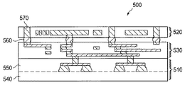
図5A〜図5Cによって表されているような他の実施形態では、ある光学的電気的システムの各部分が、別々の基板の上に形成されることがあり得る。図5Aは、ある実施形態に従って形成されたそのようなシステム500を図解している。電気コンポーネントが電気的にアクティブな基板510上に形成され、光コンポーネントが光基板520上に形成され、相互接続が相互接続基板530上に形成される。次に、基板510、520および530が面結合されて、動作可能なシステム500を形成する。
In other embodiments, as represented by FIGS. 5A-5C, each portion of an opto-electrical system may be formed on a separate substrate. FIG. 5A illustrates such a
電子基板510は、システム100の電気的機能を実装するためのトランジスタ、ダイオード、抵抗およびコンデンサなどの電子コンポーネントを含み得る。これらの機能は、限定されることはないが、スイッチング、信号調整および増幅を含むコントローラ135および175の機能を含み得る。電子基板510は、例えばシリコン・ウエハなどのベース層540と、電子デバイスと相互接続とを含むアクティブ層550とを含み得る。基板510は、任意の従来型のおよび/または将来発見されるプロセスから形成され得るのであって、どのような特定の材料のタイプにも限定されない。例示であって、限定ではないが、そのような材料は、シリコン、シリカ、SiN、InP、GaAs、銅製の相互接続、アルミニウム製の相互接続、および/または様々なバリア材料を含み得る。
光基板520は、送信段105、スイッチング段110、および受信機段115の光コンポーネントを含み得る。そのようなコンポーネントは、例えば、格子カプラ、AWG、光導波管、マイクロキャビティ共振器、光パワー・スプリッタ、光パワー・コンバイナおよびフォトダイオードなどを含む。光導波管は、従来型のおよび/または新規なプロセスによって、プレーナまたは隆起構造から形成され得る。そのようなコンポーネントは、光コア領域と光クラッド領域とを含むのが典型的である。コア領域は、例えば、シリカ、シリコン、LiNbO3、GaAlAsやGaAlNもしくはInPなどの化合物半導体合金、または電気的光学的ポリマなど、任意の従来型または非従来型の光材料系から形成され得る。本明細書で説明されているいくつかの実施形態は、非限定的な例であるシリコン(Si)に実装されている。本発明の範囲に属する実施形態はSiに限定されないが、この材料は、他の材料系と比較すると、例えば、比較的低コストであること、十分に進んだ製造用インフラストラクチャが存在すること、のようないくつかの利点を提供する。クラッド領域は、例えばシリカやベンゾシクロブテン(BCB)などの均一または不均一な誘電性材料を含み得る。クラッド領域のいくつかの部分は空気を含み得るのであるが、ここでの議論の目的として真空も含まれる。
The
相互接続基板530は、システム500の動作を構成し得る追加的な相互接続構造を含む。相互接続基板530は、所望の接続性を実装するのに必要とされる任意の誘電性材料と導電性(例えば金属製の)材料とを含み得る。いくつかの場合には、基板530の形成は、機械的なサポートを提供するハンドル・ウエハを用いることを含み得るが、その後では、基板530はハンドルから取り外される。
電子基板510は、例えばバンプ・プロセスによって、または、図解されているようなウエハ・ボンディング・プロセスによって、相互接続基板530に結合され得る。これらのプロセスは、半導体製造の当業者に広く知られており、例えば、ボンディングのために基板表面を準備するための化学的機械的研磨(CMP)を含み得る。相互接続基板530は、例えば、図5Aに図解されているバンプ・プロセスによって、または、図5Bに図解されているウエハ・ボンディング・プロセスによって、光基板520に結合され得る。バンプ・プロセスでは、半田ボール560が、基板530における相互接続構造を、光基板520におけるメタライゼーション処理がなされたバイア(via)構造570に結合する。バイア構造570は、基板520と基板530との間において、電気的および/または機械的な接続を提供し得る。
The
図5Cは、システム100の別の実施形態を図解しているのであるが、この実施形態では、相互接続と光機能とが、一体化された基板580の中に組み合わされている。図解されている実施形態では、基板580は、光基板520と、光基板520の両側に形成されている相互接続層530aおよび530bとを含む。一体化された基板580は、例えばウエハ・ボンディングによって、基板510に結合され得る。
FIG. 5C illustrates another embodiment of the
電子基板510と相互接続基板530と光基板520とが別個に形成されることによって、いくつかの目的の中の少なくとも1つにおいて役立つことがある。第1に、例えば光基板520における高品質の導波管などのいくつかの特徴を形成するのに要求される熱収支(budget)により、電気的にアクティブな基板510におけるトランジスタのドーピング・プロファイルなどの他の特徴と互換性がない可能性がある。第2に、基板510、520および530は、特定の技能および/または製造設備を有する企業によって別々に形成され、別の企業によって結合されることが可能である。第3に、組み立てられたシステム500の機能に関するセキュリティが望まれる場合であっても、どの1つの企業もデバイスの特定の機能性を判断するのに十分な知識を取得することがないように、製造作業を、様々な企業に割り当てることが可能である。このようにして、最終的な組み立ては、組み立てられたシステム500の動作に関する機密性が保証される安全な状況の下で、完成され得るのである。
The
次に図6を参照すると、例えば、様々な実施形態によるシステム100を形成するための方法600が与えられている。方法600のステップは、例えば図1〜図5においてなど、本明細書で既に説明された要素を参照することによって、限定されることなく、説明される。方法600のステップは、図解されている順序とは異なる順序で実行されることがあり得るし、いくつかの実施形態では、完全に省略されること、および/または、同時もしくは並列的なグループとして実行されることがあり得る。この方法600は、異なる基板における別個の処理によるなど、そのステップが連続的に実行されるものとして、限定されることなく、図解されている。他の実施形態、例えば共通の複合基板を用いる実施形態では、部分的に並列的にまたは完全に並列的に、そして任意の順序で、ステップを実行することもあり得る。
With reference now to FIG. 6, for example, a
ステップ610では、例えば導波管120−1などの入力導波管が形成され、例えば波長デマルチプレクサ145などの波長デマルチプレクサに光学的に接続される。ステップ620では、第1の入力組のマイクロキャビティ共振器のマイクロキャビティ共振器が、形成される。これらの共振器は、それぞれのマイクロキャビティ共振器が入力導波管の内部を伝搬する複数の周波数チャネルの中の対応する1つに制御可能に結合するように構成されるように、入力導波管に隣接して配置されている。
In
方法600のいくつかの実施形態は、複数の出力導波管が形成されるステップ630を含む。それぞれの導波管は、波長デマルチプレクサに光学的に接続されている。波長デマルチプレクサは、それぞれのキャリア信号を出力導波管の中の対応する1つにルーティングするように、構成されている。
Some embodiments of the
そのような実施形態のいくつかは、複数の出力マイクロキャビティ共振器の組が形成されるステップ640を含む。それぞれの共振器の組は、対応する複数のマイクロキャビティ共振器を含む。それぞれの出力の組の中のそれぞれのマイクロキャビティ共振器は、それぞれの組のマイクロキャビティ共振器が対応する出力導波管の内部を伝搬する対応する異なる波長チャネルと制御可能に結合し得るように、出力導波管の中の同じ対応する1つに隣接して配置されている。 Some such embodiments include a step 640 in which a plurality of output microcavity resonator sets are formed. Each resonator set includes a corresponding plurality of microcavity resonators. Each microcavity resonator in each output set can be controllably coupled to a corresponding different wavelength channel that propagates within the corresponding output waveguide. , Adjacent to the same corresponding one of the output waveguides.
図7は、例えばシステム100を形成する方法700を与えている。方法700のステップは、例えば図1〜図5など、本明細書において既に説明された要素を参照することによって、限定されることなく、説明される。方法700のステップは、図解されている順序とは異なる順序で実行されることがあり得るし、いくつかの実施形態では、完全に省略されること、および/または、並列的にもしくは並列的なグループとして実行されることがあり得る。本明細書および特許請求の範囲では、「提供される」または「提供する」とは、デバイス、基板、構造的要素などが、開示されている方法を実行する個人もしくは企業によって製造され得ること、または、別の個人もしくは企業を含む個人もしくは企業とは異なるソースからそのようにして取得され得ること、を意味する。
FIG. 7 provides a
この方法は、第1の基板が提供されるステップ710を含む。この基板は、波長デマルチプレクサに光学的に接続された入力導波管を有する。複数のマイクロキャビティ共振器を含む第1の入力マイクロキャビティ共振器の組は、入力導波管に隣接して配置されている。
The method includes a
ステップ720では、第2の基板が提供される。第2の基板は、その上に電子コントローラが形成されている。このコントローラは、マイクロキャビティ共振器のそれぞれを、入力導波管の内部を伝搬する光信号の複数の周波数チャネルの中の対応する1つに制御可能に結合するように、マイクロキャビティ共振器を制御できるように構成されている。
In
ステップ730では、第1および第2の基板が結合され、それによって、コントローラをマイクロキャビティ共振器に接続する。
In
本出願と関係する技術分野の当業者であれば、他のおよび更なる追加、削除、置換および修正を、説明されている実施形態に対して行い得ることを、理解するであろう。 Those skilled in the art to which this application relates will appreciate that other and further additions, deletions, substitutions and modifications may be made to the described embodiments.
Claims (10)
第2の複数の別々の組の光リング共振器と、
1組の光入力と1組の光出力とを有する光マルチプレクサ/デマルチプレクサと、
を備えており、
前記第1の複数の別々の組の中のそれぞれの組は、前記光マルチプレクサ/デマルチプレクサの前記光入力の中の対応する1つに光学的に接続されており、
前記第2の複数の別々の組の中のそれぞれの組は、前記光マルチプレクサ/デマルチプレクサの前記光出力の中の対応する1つに光学的に接続されている、システム。 A first plurality of separate sets of optical ring resonators;
A second plurality of separate sets of optical ring resonators;
An optical multiplexer / demultiplexer having a set of optical inputs and a set of optical outputs;
With
Each of the first plurality of separate sets is optically connected to a corresponding one of the optical inputs of the optical multiplexer / demultiplexer;
A system wherein each set in the second plurality of separate sets is optically connected to a corresponding one of the optical outputs of the optical multiplexer / demultiplexer.
それぞれのマイクロキャビティ共振器が前記入力導波管の内部を伝搬する光信号の複数の波長チャネルの中の対応する1つに結合することができるように、前記入力導波管に隣接して配置されている複数のマイクロキャビティ共振器を含む第1のマイクロキャビティ共振器の組と、
を備えている、システム。 An input waveguide optically connected to the input of the optical demultiplexer;
Arranged adjacent to the input waveguide such that each microcavity resonator can be coupled to a corresponding one of a plurality of wavelength channels of an optical signal propagating within the input waveguide. A first set of microcavity resonators comprising a plurality of microcavity resonators being configured;
System.
それぞれのマイクロキャビティ共振器が前記入力導波管の内部を伝搬する複数の波長チャネルの中の対応する1つに結合することができるように、前記入力導波管に隣接して配置されている複数のマイクロキャビティ共振器を含む第1の入力マイクロキャビティ共振器の組を提供するステップと、
を含む、方法。 Providing an input waveguide optically connected to the wavelength demultiplexer;
Each microcavity resonator is disposed adjacent to the input waveguide such that each microcavity resonator can be coupled to a corresponding one of a plurality of wavelength channels propagating within the input waveguide. Providing a first set of input microcavity resonators comprising a plurality of microcavity resonators;
Including a method.
その上に電子コントローラが形成されている第2の基板を提供するステップであって、前記電子コントローラは、周波数チャネルの中の対応する1つに制御可能に結合するように前記マイクロキャビティ共振器を制御できるように構成されている、ステップと、
前記第1の基板と前記第2の基板とを結合することにより、前記コントローラを前記マイクロキャビティ共振器に接続するステップと、
を含む方法。 A first input microcavity set comprising an input waveguide optically connected to a wavelength demultiplexer and a plurality of microcavity resonators disposed adjacent to the input waveguide Providing a first substrate, wherein each of the microcavity resonators is configured to couple to different frequencies of an optical signal propagating within the input waveguide; and
Providing a second substrate having an electronic controller formed thereon, the electronic controller configured to controllably couple the microcavity resonator to a corresponding one of the frequency channels. A step configured to be controllable, and
Connecting the controller to the microcavity resonator by coupling the first substrate and the second substrate;
Including methods.
Applications Claiming Priority (9)
| Application Number | Priority Date | Filing Date | Title |
|---|---|---|---|
| US201261667380P | 2012-07-02 | 2012-07-02 | |
| US201261667374P | 2012-07-02 | 2012-07-02 | |
| US61/667,380 | 2012-07-02 | ||
| US61/667,374 | 2012-07-02 | ||
| US13/800,634 US20140003810A1 (en) | 2012-07-02 | 2013-03-13 | Reconfigurable optical networks |
| US13/800,403 | 2013-03-13 | ||
| US13/800,403 US9164300B2 (en) | 2012-07-02 | 2013-03-13 | Reconfigurable optical networks |
| US13/800,634 | 2013-03-13 | ||
| PCT/US2013/047455 WO2014008028A1 (en) | 2012-07-02 | 2013-06-25 | Reconfigurable optical networks |
Publications (1)
| Publication Number | Publication Date |
|---|---|
| JP2015526966A true JP2015526966A (en) | 2015-09-10 |
Family
ID=49778272
Family Applications (3)
| Application Number | Title | Priority Date | Filing Date |
|---|---|---|---|
| JP2015520376A Pending JP2015526965A (en) | 2012-07-02 | 2013-06-25 | Reconfigurable optical network |
| JP2015520377A Withdrawn JP2015526966A (en) | 2012-07-02 | 2013-06-25 | Reconfigurable optical network |
| JP2017046353A Pending JP2017143533A (en) | 2012-07-02 | 2017-03-10 | Reconfigurable Optical Network |
Family Applications Before (1)
| Application Number | Title | Priority Date | Filing Date |
|---|---|---|---|
| JP2015520376A Pending JP2015526965A (en) | 2012-07-02 | 2013-06-25 | Reconfigurable optical network |
Family Applications After (1)
| Application Number | Title | Priority Date | Filing Date |
|---|---|---|---|
| JP2017046353A Pending JP2017143533A (en) | 2012-07-02 | 2017-03-10 | Reconfigurable Optical Network |
Country Status (7)
| Country | Link |
|---|---|
| US (2) | US9164300B2 (en) |
| EP (2) | EP2868018A1 (en) |
| JP (3) | JP2015526965A (en) |
| KR (2) | KR20150016611A (en) |
| CN (2) | CN104769872A (en) |
| IN (2) | IN2014DN10746A (en) |
| WO (2) | WO2014008027A1 (en) |
Families Citing this family (24)
| Publication number | Priority date | Publication date | Assignee | Title |
|---|---|---|---|---|
| US9164300B2 (en) | 2012-07-02 | 2015-10-20 | Alcatel Lucent | Reconfigurable optical networks |
| US20150253502A1 (en) * | 2012-09-13 | 2015-09-10 | Ben-Gurion University Of The Negev Research And Development Authority | Integrated circuit with photonic elements |
| US20150336372A1 (en) * | 2013-05-28 | 2015-11-26 | Claude Louis Van Ness | Screen Printing Device and Method |
| EP3042463B1 (en) * | 2013-09-04 | 2017-05-31 | Telefonaktiebolaget LM Ericsson (publ) | Optical switch, optical add-drop multiplexer, communication network node and communication network |
| JP6249837B2 (en) * | 2014-03-17 | 2017-12-20 | 富士通株式会社 | Control method of optical element |
| US9698457B2 (en) * | 2014-07-28 | 2017-07-04 | The University Of Connecticut | Optoelectronic integrated circuitry for transmitting and/or receiving wavelength-division multiplexed optical signals |
| TWI603594B (en) * | 2014-09-19 | 2017-10-21 | 財團法人工業技術研究院 | Optical communication device and optical communication method |
| EP3016402A1 (en) * | 2014-10-31 | 2016-05-04 | Hewlett-Packard Development Company, L.P. | Optical circuit switch |
| US9762479B2 (en) * | 2014-11-10 | 2017-09-12 | Maged E. Beshai | Distributed routing control in a vast communication network |
| GB2535236A (en) * | 2015-02-16 | 2016-08-17 | Ge Oil & Gas Uk Ltd | Retrofit power switching and repeating module |
| US10820071B2 (en) | 2015-08-13 | 2020-10-27 | Hewlett Packard Enterprise Development Lp | Reconfigurable interconnected nodes |
| WO2017027042A1 (en) * | 2015-08-13 | 2017-02-16 | Hewlett Packard Enterprise Development Lp | Reconfigurable interconnected nodes |
| US9366822B1 (en) * | 2015-09-29 | 2016-06-14 | Sandia Corporation | Thermo-optically tuned photonic resonators with concurrent electrical connection and thermal isolation |
| CN106936506B (en) * | 2015-12-30 | 2019-05-24 | 华为技术有限公司 | A kind of optical node and related system |
| US20180035090A1 (en) * | 2016-03-15 | 2018-02-01 | Sutherland Cook Ellwood, JR. | Photonic signal converter |
| CA3025833A1 (en) * | 2016-06-01 | 2017-12-07 | Roshmere, Inc. | An optically-switched data network |
| US9991966B1 (en) * | 2017-01-06 | 2018-06-05 | Huawei Technologies Canada Co., Ltd. | Optical transmitter |
| US11957261B2 (en) | 2017-04-28 | 2024-04-16 | Lutron Technology Company Llc | Window treatment mounting bracket |
| KR102338923B1 (en) | 2017-07-06 | 2021-12-14 | 삼성전자주식회사 | Photonic integrated circuit and optical transmitter |
| US10200144B1 (en) * | 2017-09-15 | 2019-02-05 | Nokia Of America Corporation | Communication system for connecting network hosts |
| US11101912B2 (en) * | 2018-07-12 | 2021-08-24 | Ayar Labs, Inc. | Electro-optical interface module and associated methods |
| US11139907B2 (en) | 2018-11-07 | 2021-10-05 | Nokia Solutions And Networks Oy | Methods and apparatus for tuning optical microring devices |
| GB2582971B (en) * | 2019-04-12 | 2021-07-07 | Rockley Photonics Ltd | Switch with a shuffle |
| US20220075114A1 (en) * | 2020-09-04 | 2022-03-10 | Ciena Corporation | Resonant device improvement in PICs using spare devices to reduce power requirements |
Family Cites Families (39)
| Publication number | Priority date | Publication date | Assignee | Title |
|---|---|---|---|---|
| JP3114801B2 (en) | 1997-07-07 | 2000-12-04 | 日本電気株式会社 | Optical communication network equipment |
| US6195187B1 (en) * | 1998-07-07 | 2001-02-27 | The United States Of America As Represented By The Secretary Of The Air Force | Wavelength-division multiplexed M×N×M cross-connect switch using active microring resonators |
| US6580534B2 (en) * | 1999-01-27 | 2003-06-17 | Lucent Technologies Inc. | Optical channel selector |
| WO2000050938A1 (en) * | 1999-02-22 | 2000-08-31 | Massachusetts Institute Of Technology | Vertically coupled optical resonator devices over a cross-grid waveguide architecture |
| US20030128980A1 (en) | 2002-11-27 | 2003-07-10 | Abeles Joseph H. | Channelizer switch |
| US7894418B2 (en) | 2002-08-15 | 2011-02-22 | The Boeing Company | Mixed analog and digital chip-scale reconfigurable WDM network |
| US7088919B2 (en) | 2002-11-04 | 2006-08-08 | Nortel Networks Limited | Modular photonic switch with wavelength conversion |
| US7313329B2 (en) | 2003-09-04 | 2007-12-25 | The Regents Of The University Of California | All optical variable buffer queue useful in optical packet networks |
| US7203387B2 (en) * | 2003-09-10 | 2007-04-10 | Agency For Science, Technology And Research | VLSI-photonic heterogeneous integration by wafer bonding |
| US20080165565A1 (en) | 2004-01-12 | 2008-07-10 | Eidgenossische Technische Hochschule Zurich | Ferroelectric Thin Films and Devices Comprising Thin Ferroelectric Films |
| JP5059601B2 (en) | 2004-04-15 | 2012-10-24 | インフィネラ コーポレイション | Coolerless integrated circuit and floating wavelength grid photonic integrated circuit (PIC) for WDM transmission networks |
| WO2005106551A1 (en) | 2004-04-30 | 2005-11-10 | Pirelli & C. S.P.A. | An optical device based on a three-arm mach-zehnder interferometer |
| US7539418B1 (en) | 2005-09-16 | 2009-05-26 | Sun Microsystems, Inc. | Integrated ring modulator array WDM transceiver |
| US7720377B2 (en) * | 2006-01-23 | 2010-05-18 | Hewlett-Packard Development Company, L.P. | Compute clusters employing photonic interconnections for transmitting optical signals between compute cluster nodes |
| US20070280577A1 (en) | 2006-05-25 | 2007-12-06 | Way-Seen Wang | Optical multi-wavelength modulator |
| US8295655B2 (en) | 2006-08-24 | 2012-10-23 | Cornell Research Foundation, Inc. | Electro-optical modulator |
| US7970244B2 (en) | 2006-09-11 | 2011-06-28 | The Boeing Company | Fabrication of an optical ring resonator device |
| US7421168B1 (en) | 2007-07-02 | 2008-09-02 | Northrop Grumman Systems Corporation | Integrated optical channelizer |
| US8027587B1 (en) | 2007-08-21 | 2011-09-27 | Sandia Corporation | Integrated optic vector-matrix multiplier |
| WO2009055032A2 (en) | 2007-10-23 | 2009-04-30 | Hewlett-Packard Development Company, L.P. | All optical fast distributed arbitration in a computer system device |
| US7945165B2 (en) * | 2007-11-16 | 2011-05-17 | Alcatel-Lucent Usa Inc. | Optical signal synchronizer |
| US8073333B2 (en) * | 2007-11-16 | 2011-12-06 | Alcatel Lucent | Multiplex delay unit |
| US20090161113A1 (en) * | 2007-12-19 | 2009-06-25 | Young-Kai Chen | Integrated optoelectronic system for automatic calibration of an optical device |
| JP4901768B2 (en) | 2008-01-18 | 2012-03-21 | 株式会社東芝 | Optical multiplexer / demultiplexer |
| US8938139B2 (en) | 2008-03-11 | 2015-01-20 | Hewlett-Packard Development Company, L.P. | Optoelectronic switches using on-chip optical waveguides |
| EP2371044B1 (en) | 2008-12-03 | 2019-08-28 | Innolume GmbH | Semiconductor laser with low relative intensity noise of individual longitudinal modes and optical transmission system incorporating the laser |
| US8660390B2 (en) | 2009-01-27 | 2014-02-25 | Hewlett-Packard Development Company, L.P. | Redundant ring resonators of varying dimensions to reduce ring resonator tuning requirements |
| US8705972B2 (en) * | 2010-05-11 | 2014-04-22 | Hewlett-Packard Development Company, L.P. | Energy-efficient and fault-tolerant resonator-based modulation and wavelength division multiplexing systems |
| US9054493B2 (en) | 2010-06-22 | 2015-06-09 | Oracle International Corporation | Multiple-wavelength laser |
| US9753349B2 (en) * | 2010-08-20 | 2017-09-05 | University Of Rochester | Optical circuit apparatus, method, and application |
| US9819435B2 (en) | 2010-08-26 | 2017-11-14 | Cornell University | Optical apparatus, method, and applications |
| US20120146646A1 (en) | 2010-12-09 | 2012-06-14 | General Electric Company | Nanophotonic system for optical data and power transmission in medical imaging systems |
| US8594471B2 (en) | 2011-03-30 | 2013-11-26 | Telefonaktiebolaget L M Ericsson (Publ) | Adaptive waveguide optical switching system and method |
| US8847598B2 (en) | 2011-07-08 | 2014-09-30 | General Electric Company | Photonic system and method for optical data transmission in medical imaging systems |
| US8625936B1 (en) * | 2012-06-29 | 2014-01-07 | Alcatel Lucent | Advanced modulation formats using optical modulators |
| US8588556B1 (en) | 2012-06-29 | 2013-11-19 | Alcatel Lucent | Advanced modulation formats using optical modulators |
| US9164300B2 (en) | 2012-07-02 | 2015-10-20 | Alcatel Lucent | Reconfigurable optical networks |
| US20140270621A1 (en) * | 2013-03-15 | 2014-09-18 | Apic Corporation | Photonic multi-chip module |
| US9020347B2 (en) * | 2013-09-09 | 2015-04-28 | Oracle International Corporation | Reconfigurable optical interconnect network |
-
2013
- 2013-03-13 US US13/800,403 patent/US9164300B2/en not_active Expired - Fee Related
- 2013-03-13 US US13/800,634 patent/US20140003810A1/en not_active Abandoned
- 2013-06-25 JP JP2015520376A patent/JP2015526965A/en active Pending
- 2013-06-25 CN CN201380035368.5A patent/CN104769872A/en active Pending
- 2013-06-25 CN CN201380035296.4A patent/CN104604168A/en active Pending
- 2013-06-25 JP JP2015520377A patent/JP2015526966A/en not_active Withdrawn
- 2013-06-25 EP EP13739879.8A patent/EP2868018A1/en not_active Withdrawn
- 2013-06-25 IN IN10746DEN2014 patent/IN2014DN10746A/en unknown
- 2013-06-25 WO PCT/US2013/047454 patent/WO2014008027A1/en active Application Filing
- 2013-06-25 WO PCT/US2013/047455 patent/WO2014008028A1/en active Application Filing
- 2013-06-25 EP EP13740094.1A patent/EP2868019A1/en not_active Withdrawn
- 2013-06-25 IN IN10812DEN2014 patent/IN2014DN10812A/en unknown
- 2013-06-25 KR KR1020147036945A patent/KR20150016611A/en not_active Application Discontinuation
- 2013-06-25 KR KR1020147037064A patent/KR20150016619A/en not_active Application Discontinuation
-
2017
- 2017-03-10 JP JP2017046353A patent/JP2017143533A/en active Pending
Also Published As
| Publication number | Publication date |
|---|---|
| JP2017143533A (en) | 2017-08-17 |
| WO2014008028A1 (en) | 2014-01-09 |
| EP2868018A1 (en) | 2015-05-06 |
| US9164300B2 (en) | 2015-10-20 |
| KR20150016619A (en) | 2015-02-12 |
| WO2014008027A1 (en) | 2014-01-09 |
| JP2015526965A (en) | 2015-09-10 |
| IN2014DN10746A (en) | 2015-09-04 |
| US20140003810A1 (en) | 2014-01-02 |
| IN2014DN10812A (en) | 2015-09-04 |
| CN104769872A (en) | 2015-07-08 |
| US20140003760A1 (en) | 2014-01-02 |
| KR20150016611A (en) | 2015-02-12 |
| EP2868019A1 (en) | 2015-05-06 |
| CN104604168A (en) | 2015-05-06 |
Similar Documents
| Publication | Publication Date | Title |
|---|---|---|
| JP2015526966A (en) | Reconfigurable optical network | |
| TWI472820B (en) | Core-selective optical switches and method of forming thereof | |
| JP3256419B2 (en) | Optical filter and optical signal transmission system | |
| US11101913B2 (en) | Processing of multimode optical signals | |
| US7200299B1 (en) | Adding and dropping wavelength-channels | |
| US20120063778A1 (en) | Optical Add/Drop Multiplexer Using Integrated Optical Components | |
| JP6008984B2 (en) | Dual polarization multiwavelength coherent receiver front end | |
| CN105229953A (en) | The radix of photon packet switch strengthens | |
| US6549313B1 (en) | Broadbrand electronic N×N cross-connect switch using tunable lasers | |
| JP3593291B2 (en) | WDM network | |
| CN114114529A (en) | Optical redistribution layer for high channel count photonics | |
| KR101329875B1 (en) | System and method for demultiplexing optical multi-wavelength signals | |
| US11811455B2 (en) | Device and method for processing an optical signal | |
| TW202225750A (en) | Optical data communication system and associated method | |
| CN111052759B (en) | All optical network based on Switchable Wavelength Connection (SWC) | |
| Testa et al. | Silicon photonics for telecom and datacom applications | |
| JP2018074273A (en) | Network system | |
| Xiao et al. | Experimental demonstration of SiPh Flex-LIONS for bandwidth-reconfigurable optical interconnects | |
| TW201320646A (en) | Transmitter and method for optical transmission | |
| WO2023164213A1 (en) | Optical communication system with simplified remote optical power supply | |
| JP4001825B2 (en) | Semiconductor optical device for wavelength division multiplexing | |
| JP2005117507A (en) | Optical communication network system | |
| JPH03226137A (en) | Optical wavelength split multiple communication system and communication network |
Legal Events
| Date | Code | Title | Description |
|---|---|---|---|
| A761 | Written withdrawal of application |
Free format text: JAPANESE INTERMEDIATE CODE: A761 Effective date: 20150820 |