JP2015210323A - Lighting unit, lighting control method, and display device - Google Patents
Lighting unit, lighting control method, and display device Download PDFInfo
- Publication number
- JP2015210323A JP2015210323A JP2014090316A JP2014090316A JP2015210323A JP 2015210323 A JP2015210323 A JP 2015210323A JP 2014090316 A JP2014090316 A JP 2014090316A JP 2014090316 A JP2014090316 A JP 2014090316A JP 2015210323 A JP2015210323 A JP 2015210323A
- Authority
- JP
- Japan
- Prior art keywords
- signal
- blpwm
- control signal
- value
- bits
- Prior art date
- Legal status (The legal status is an assumption and is not a legal conclusion. Google has not performed a legal analysis and makes no representation as to the accuracy of the status listed.)
- Pending
Links
Images

Classifications
-
- G—PHYSICS
- G09—EDUCATION; CRYPTOGRAPHY; DISPLAY; ADVERTISING; SEALS
- G09G—ARRANGEMENTS OR CIRCUITS FOR CONTROL OF INDICATING DEVICES USING STATIC MEANS TO PRESENT VARIABLE INFORMATION
- G09G3/00—Control arrangements or circuits, of interest only in connection with visual indicators other than cathode-ray tubes
- G09G3/20—Control arrangements or circuits, of interest only in connection with visual indicators other than cathode-ray tubes for presentation of an assembly of a number of characters, e.g. a page, by composing the assembly by combination of individual elements arranged in a matrix no fixed position being assigned to or needed to be assigned to the individual characters or partial characters
- G09G3/34—Control arrangements or circuits, of interest only in connection with visual indicators other than cathode-ray tubes for presentation of an assembly of a number of characters, e.g. a page, by composing the assembly by combination of individual elements arranged in a matrix no fixed position being assigned to or needed to be assigned to the individual characters or partial characters by control of light from an independent source
- G09G3/3406—Control of illumination source
-
- G—PHYSICS
- G09—EDUCATION; CRYPTOGRAPHY; DISPLAY; ADVERTISING; SEALS
- G09G—ARRANGEMENTS OR CIRCUITS FOR CONTROL OF INDICATING DEVICES USING STATIC MEANS TO PRESENT VARIABLE INFORMATION
- G09G2320/00—Control of display operating conditions
- G09G2320/06—Adjustment of display parameters
- G09G2320/0626—Adjustment of display parameters for control of overall brightness
- G09G2320/064—Adjustment of display parameters for control of overall brightness by time modulation of the brightness of the illumination source
-
- G—PHYSICS
- G09—EDUCATION; CRYPTOGRAPHY; DISPLAY; ADVERTISING; SEALS
- G09G—ARRANGEMENTS OR CIRCUITS FOR CONTROL OF INDICATING DEVICES USING STATIC MEANS TO PRESENT VARIABLE INFORMATION
- G09G2320/00—Control of display operating conditions
- G09G2320/06—Adjustment of display parameters
- G09G2320/0626—Adjustment of display parameters for control of overall brightness
- G09G2320/0646—Modulation of illumination source brightness and image signal correlated to each other
Landscapes
- Engineering & Computer Science (AREA)
- Physics & Mathematics (AREA)
- Computer Hardware Design (AREA)
- General Physics & Mathematics (AREA)
- Theoretical Computer Science (AREA)
- Control Of Indicators Other Than Cathode Ray Tubes (AREA)
- Liquid Crystal Display Device Control (AREA)
- Liquid Crystal (AREA)
- Multimedia (AREA)
Abstract
Description
照明装置、照明制御方法および表示装置に関する。 The present invention relates to an illumination device, an illumination control method, and a display device.
近年、RGBW方式を採用した液晶パネル表示が開発されている。これは、通常のR(赤)、G(緑)、B(青)の画素に対して、W(白)の画素を追加して1つの画素を構成するものである。これにより、W画素の輝度を向上させる分、液晶パネルを背面等から照明するバックライトの輝度を下げることができ、装置全体の消費電力の低減化を可能にしている。 In recent years, liquid crystal panel displays employing the RGBW method have been developed. In this configuration, one pixel is configured by adding W (white) pixels to normal R (red), G (green), and B (blue) pixels. As a result, the brightness of the backlight for illuminating the liquid crystal panel from the back surface or the like can be lowered by the amount of improvement in the brightness of the W pixel, and the power consumption of the entire apparatus can be reduced.
一方、上記のような表示方式では、バックライトの輝度の制御に伴って、画品位の低下が生じる場合がある。このため、例えば、画像信号に適した発光輝度となるように設定した輝度設定値を含む変換テーブルを用いて、輝度設定値をバックライト制御値に変換して、バックライトに供給する技術が提案されている(特許文献1)。 On the other hand, in the display method as described above, there is a case where the image quality is lowered with the control of the luminance of the backlight. For this reason, for example, a technique is proposed in which a brightness setting value is converted into a backlight control value using a conversion table including a brightness setting value set so as to have a light emission brightness suitable for an image signal, and is supplied to the backlight. (Patent Document 1).
または、1画面毎の画像の平均輝度と、輝度調整直線とから、バックライト輝度を調整するための調整値を計算し、調整値に応じてバックライトを駆動するための信号を発生させて、バックライト輝度を制御する技術が提案されている(特許文献2)。 Alternatively, an adjustment value for adjusting the backlight luminance is calculated from the average luminance of the image for each screen and the luminance adjustment line, and a signal for driving the backlight according to the adjustment value is generated. A technique for controlling backlight luminance has been proposed (Patent Document 2).
本発明は、画品位低下の改善を図った照明装置、照明制御方法および表示装置を提供する。または高精度な輝度制御を実現した照明装置、照明制御方法および表示装置を提供する。 The present invention provides an illumination device, an illumination control method, and a display device that are improved in image quality degradation. Alternatively, an illumination device, an illumination control method, and a display device that realize high-accuracy brightness control are provided.
本発明の一態様は、光源と、前記光源の輝度を制御するための、第1のビット数の第1の輝度制御信号に対して、前記第1の輝度制御信号で表現される値を、前記第1のビット数よりも小さな第2のビット数を持つ第2の輝度制御信号で時分割し、前記第2の輝度制御信号で表現される値に対応するパルス幅を持つ第3の輝度制御信号を生成する時分割制御部と、前記第3の輝度制御信号にもとづいて、前記光源を発光させるための駆動信号を生成して、前記光源へ供給する駆動部とを有する照明装置である。 One embodiment of the present invention is directed to a light source and a value represented by the first luminance control signal with respect to a first luminance control signal having a first number of bits for controlling the luminance of the light source. A third luminance having a pulse width corresponding to a value represented by the second luminance control signal, time-divided by a second luminance control signal having a second bit number smaller than the first bit number. A lighting device comprising: a time division control unit that generates a control signal; and a drive unit that generates a drive signal for causing the light source to emit light based on the third luminance control signal and supplies the drive signal to the light source. .
以下に、本発明の各実施の形態について、図面を参照しつつ説明する。 Hereinafter, embodiments of the present invention will be described with reference to the drawings.
なお、開示はあくまでも一例にすぎず、当業者において、発明の主旨を保っての適宜変更について容易に想到し得るものについては、当然に本発明の範囲に含有されるものである。また、図面は説明をより明確にするため、実際の態様に比べ、各部の幅、厚さ、形状等について模式的に表される場合があるが、あくまで一例であって、本発明の解釈を限定するものではない。 It should be noted that the disclosure is merely an example, and those skilled in the art can easily conceive of appropriate changes while maintaining the gist of the invention are naturally included in the scope of the present invention. In addition, the drawings may be schematically represented with respect to the width, thickness, shape, and the like of each part in comparison with actual aspects for the sake of clarity of explanation, but are merely examples, and the interpretation of the present invention is not limited. It is not limited.
また、本発明と各図において、既出の図に関して前述したものと同様の要素には、同一の符号を付して、詳細な説明を適宜省略することがある。 In the present invention and each drawing, the same reference numerals are given to the same elements as those described above with reference to the previous drawings, and the detailed description may be omitted as appropriate.
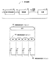
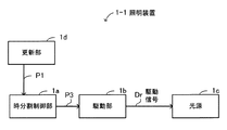
まず、本発明を図1を用いて簡潔に説明する。図1は照明装置の構成例を示す図である。照明装置1は、時分割制御部1a、駆動部1bおよび表示パネル等に使用される照明用の光源1cを備える。
First, the present invention will be briefly described with reference to FIG. FIG. 1 is a diagram illustrating a configuration example of a lighting device. The
時分割制御部1aは、光源1cの輝度を制御するための、第1のビット数の輝度制御信号P1(第1の輝度制御信号)に対して、輝度制御信号P1で表現される値を、第1のビット数よりも小さな第2のビット数を持つ輝度制御信号P2(第2の輝度制御信号)で時分割する。
The time
そして、時分割制御部1aは、時分割した輝度制御信号P2で表現される各値に対応するパルス幅を持つ輝度制御信号P3(第3の輝度制御信号)を生成する。
Then, the time
駆動部1bは、輝度制御信号P3にもとづいて、光源1cを発光させるための駆動信号Drを生成して、光源1cへ供給する。
The
ここで、図1に示す時分割制御の例では、第1のビット数を10ビット、第2のビット数を8ビットとすると、10ビットの輝度制御信号P1で表現される257という値に対して、4つに時分割した64、64、64、65という値の8ビットの輝度制御信号P2が生成されている。 Here, in the example of time division control shown in FIG. 1, when the first bit number is 10 bits and the second bit number is 8 bits, the value of 257 expressed by the 10-bit luminance control signal P1 is obtained. Thus, an 8-bit luminance control signal P2 having a value of 64, 64, 64, 65 divided into four is generated.
また、64という値の輝度制御信号P2に対してはパルス幅(の長さ)がw1、65という値の輝度制御信号P2に対してはパルス幅がw2(>w1)という、1ビットの輝度制御信号P3が生成されている。 In addition, for the luminance control signal P2 having the value of 64, the pulse width (length) is w1, and for the luminance control signal P2 having the value of 65, the pulse width is w2 (> w1). A control signal P3 is generated.
このように、照明装置1では、第1のビット数の輝度制御信号P1で表現される値を、第1のビット数よりも小さな第2のビット数を持つ輝度制御信号P2で時分割して表現し、輝度制御信号P2で表現される各値に対応するパルス幅を持つ輝度制御信号P3を生成する。
Thus, in the
そして、照明装置1では、輝度制御信号P3にもとづいて、光源1cを発光させる駆動信号Drを生成して光源1cへ供給する。
And in the
このような制御により、画品位低下の改善を図ることが可能になり、また、バックライトに対する高精度な輝度制御を実現することが可能になる。 By such control, it becomes possible to improve the image quality deterioration, and it is possible to realize highly accurate luminance control for the backlight.
以下に、本技術の詳細を説明する。なお、本発明の詳細を説明する前に、解決すべき課題について図2〜図7を用いて説明する。液晶パネルを背面等から照明するバックライトを有する照明装置では、表示される画像に応じて、バックライトの輝度を変化させる。バックライトの輝度は、PWM(Pulse Width Modulated:パルス幅変調)信号によって制御される。 Details of the present technology will be described below. Before describing the details of the present invention, problems to be solved will be described with reference to FIGS. In an illuminating device having a backlight that illuminates the liquid crystal panel from the back or the like, the luminance of the backlight is changed according to the displayed image. The brightness of the backlight is controlled by a PWM (Pulse Width Modulated) signal.
バックライトの輝度制御(PWM制御)では、通常、パラレルビットのPWM信号を1ビットのPWM信号に変換し、1ビットのPWM信号でバックライトドライバ(BL(Back Light)ドライバ)の駆動制御を行っている。 In backlight brightness control (PWM control), a parallel bit PWM signal is usually converted into a 1-bit PWM signal, and a drive control of a backlight driver (BL (Back Light) driver) is performed using the 1-bit PWM signal. ing.
なお、以降では、パラレルビットのPWM信号をBLPWM(Back Light PWM)信号と呼ぶ。また、1ビットのPWM信号を単にPWM信号とも呼ぶ。 Hereinafter, the parallel bit PWM signal is referred to as a BLPWM (Back Light PWM) signal. A 1-bit PWM signal is also simply referred to as a PWM signal.
バックライトの輝度を細かく制御する場合、BLPWM信号のパラレルのビット数を増やして、PWM信号の分解能を細かく設定することになるが、BLPWM信号のビット数を単純に増やすと、下記のような問題が生じる。 When the backlight brightness is finely controlled, the number of parallel bits of the BLPWM signal is increased and the resolution of the PWM signal is finely set. However, if the number of bits of the BLPWM signal is simply increased, the following problems occur. Occurs.
(1)複数のビット数のBLPWM信号を、1ビットのPWM信号に変換する回路において、PWM信号の周期が伸びてしまい、バックライトのちらつき(フリッカ)の原因となる。 (1) In a circuit that converts a BLPWM signal having a plurality of bits into a 1-bit PWM signal, the period of the PWM signal is extended, which causes backlight flicker.
(2)逆に、PWM信号の周期を維持すると、1ビット当たりのPWM信号のパルス幅が狭くなり、BLドライバがその狭いパルス幅の信号に応答できずに、輝度のリニアリティが保てなくなる。 (2) Conversely, if the period of the PWM signal is maintained, the pulse width of the PWM signal per bit becomes narrow, the BL driver cannot respond to the signal with the narrow pulse width, and the luminance linearity cannot be maintained.
以下、(1)については図2〜図4を用いて、(2)については図5〜図7を用いて説明する。図2〜図4はPWM信号の周期の伸長を示す図である。 Hereinafter, (1) will be described with reference to FIGS. 2 to 4, and (2) will be described with reference to FIGS. 2 to 4 are diagrams showing the expansion of the period of the PWM signal.
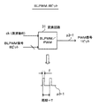
図2では、8ビットのBLPWM信号のPWM信号への変換を示している。変換回路31には、周波数f0のクロック信号ckと、8ビットのBLPWM信号とが入力し、変換回路31から1ビットのPWM信号p3−1が出力している。また、PWM信号p3−1の1周期をTとし、PWM信号p3−1のHレベルのパルス幅をτとする。 FIG. 2 shows conversion of an 8-bit BLPWM signal to a PWM signal. A clock signal ck having a frequency f0 and an 8-bit BLPWM signal are input to the conversion circuit 31, and a 1-bit PWM signal p3-1 is output from the conversion circuit 31. Further, T represents one cycle of the PWM signal p3-1 and τ represents a pulse width of the H level of the PWM signal p3-1.
図3では、10ビットのBLPWM信号のPWM信号への変換を示している。変換回路31には、周波数f0のクロック信号ckと、10ビットのBLPWM信号とが入力し、変換回路31から1ビットのPWM信号p3−2が出力している。 FIG. 3 shows conversion of a 10-bit BLPWM signal into a PWM signal. A clock signal ck having a frequency f0 and a 10-bit BLPWM signal are input to the conversion circuit 31, and a 1-bit PWM signal p3-2 is output from the conversion circuit 31.
このとき、PWM信号p3−2のHレベルのパルス幅を、図2のPWM信号p3−1のパルス幅と同じτにした場合、PWM信号p3−2の1周期は4Tとなる。 At this time, when the pulse width of the H level of the PWM signal p3-2 is set to the same τ as the pulse width of the PWM signal p3-1 in FIG. 2, one cycle of the PWM signal p3-2 is 4T.
図4では、12ビットのBLPWM信号のPWM信号への変換を示している。変換回路31には、周波数f0のクロック信号ckと、12ビットのBLPWM信号とが入力し、変換回路31から1ビットのPWM信号p3−3が出力している。 FIG. 4 shows conversion of a 12-bit BLPWM signal into a PWM signal. A clock signal ck having a frequency f0 and a 12-bit BLPWM signal are input to the conversion circuit 31, and a 1-bit PWM signal p3-3 is output from the conversion circuit 31.
このとき、PWM信号p3−3のHレベルのパルス幅を、図2のPWM信号p3−1のパルス幅と同じτにした場合、PWM信号p3−3の1周期は16Tとなる。 At this time, if the pulse width of the H level of the PWM signal p3-3 is set to the same τ as the pulse width of the PWM signal p3-1 in FIG. 2, one cycle of the PWM signal p3-3 is 16T.
ここで、BLPWM信号からPWM信号を生成する際に要するクロック信号ckのクロック数は、BLPWM信号のビット数に応じて異なるものである。 Here, the number of clocks of the clock signal ck required when generating the PWM signal from the BLPWM signal differs depending on the number of bits of the BLPWM signal.
すなわち、8ビットのBLPWM信号から1ビットのPWM信号を生成する場合は、256(=28)クロックを要する。また、10ビットのBLPWM信号から1ビットのPWM信号を生成する場合は、1024(=210)クロックを要する。さらに、12ビットのBLPWM信号から1ビットのPWM信号を生成する場合は、4096(=212)クロックを要する。 That is, when generating a 1-bit PWM signal from an 8-bit BLPWM signal, 256 (= 2 8 ) clocks are required. When generating a 1-bit PWM signal from a 10-bit BLPWM signal, 1024 (= 2 10 ) clocks are required. Further, when a 1-bit PWM signal is generated from a 12-bit BLPWM signal, 4096 (= 2 12 ) clocks are required.
これに対して、上記の変換回路31のように、入力クロック信号の周波数(クロック数)を固定にして、BLPWM信号のビット数だけ変化させ、変換回路31から出力されるPWM信号のパルス幅を、BLPWM信号の最小ビット数のときのパルス幅と同じ値にする。すると、BLPWM信号のビット数の増加に伴い、変換回路31から出力されるPWM信号の周期が伸長することになる。 On the other hand, like the conversion circuit 31 described above, the frequency (number of clocks) of the input clock signal is fixed, the number of bits of the BLPWM signal is changed, and the pulse width of the PWM signal output from the conversion circuit 31 is changed. , The pulse width is set to the same value as the minimum number of bits of the BLPWM signal. Then, as the number of bits of the BLPWM signal increases, the cycle of the PWM signal output from the conversion circuit 31 is extended.
すなわち、図2〜図4に示すように、変換回路31において、同じ周波数f0のクロック信号ckで、BLPWM信号のビット数を8、10、12ビットと上げていく。そして、10、12ビットのBLPWM信号に対しても、そのとき出力されるPWM信号のパルスの変化幅を、8ビットのBLPWM信号のときと同じパルス幅にする(上記ではHレベルを同じにしたが、Lレベルを同じにしてもよい)。 That is, as shown in FIGS. 2 to 4, in the conversion circuit 31, the number of bits of the BLPWM signal is increased to 8, 10, and 12 with the clock signal ck having the same frequency f0. For the 10 and 12-bit BLPWM signal, the pulse width of the PWM signal output at that time is set to the same pulse width as that of the 8-bit BLPWM signal (in the above, the H level is the same). However, the L level may be the same).
すると、8ビットBLPWM信号が入力されたときの変換回路31から出力されるPWM信号の1周期がTだったものが、10ビットBLPWM信号の入力では、PWM信号の1周期が4Tに伸長する。 Then, when one cycle of the PWM signal output from the conversion circuit 31 when the 8-bit BLPWM signal is input is T, one cycle of the PWM signal is extended to 4T when the 10-bit BLPWM signal is input.
また、8ビットBLPWM信号が入力されたときの変換回路31から出力されるPWM信号の1周期がTだったものが、12ビットBLPWM信号の入力では、PWM信号の1周期が16Tに伸長する。 In addition, although one cycle of the PWM signal output from the conversion circuit 31 when the 8-bit BLPWM signal is input is T, when the 12-bit BLPWM signal is input, one cycle of the PWM signal is expanded to 16T.
このように、BLPWM信号のビット数を単に増やして、バックライトの輝度を細かく制御すると、PWM信号の周期の増加(PWM信号の周波数の低下)が生じてしまう。それがバックライトの画面ちらつきの原因となり、その結果、画品位の低下を引き起こすことになる。 In this way, if the number of bits of the BLPWM signal is simply increased to finely control the backlight brightness, the PWM signal cycle will increase (the PWM signal frequency will decrease). This causes the screen flickering of the backlight, and as a result, the image quality is lowered.
図5〜図7は1ビット当たりのPWM信号のパルス幅の狭くなる現象を示す図である。BLPWM信号のどのパラレルビット数に対しても、変換出力後のPWM信号の周期を同一にした場合には、PWM信号のパルス幅が狭くなる。PWM信号のパルス幅が狭くなる理由を以下に説明する。 5 to 7 are diagrams showing a phenomenon in which the pulse width of the PWM signal per bit is narrowed. When the cycle of the PWM signal after conversion output is made the same for any number of parallel bits of the BLPWM signal, the pulse width of the PWM signal becomes narrow. The reason why the pulse width of the PWM signal becomes narrow will be described below.
なお、図中のBL電流とは、バックライトの輝度を設定するための電流信号のことであり、BLドライバがPWM信号にもとづいて生成する駆動信号である。また、BL電流がバックライトを構成するLED(Light Emitting Diode)に供給されることで、BL電流の値に応じて、バックライトの輝度が設定されることになる。 The BL current in the figure is a current signal for setting the brightness of the backlight, and is a drive signal generated by the BL driver based on the PWM signal. Further, the brightness of the backlight is set according to the value of the BL current by supplying the BL current to an LED (Light Emitting Diode) constituting the backlight.
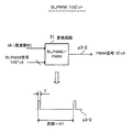
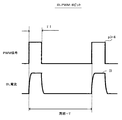
図5では、8ビットのBLPWM信号に対する、変換出力後のPWM信号p3−4と、PWM信号p3−4にもとづき、BLドライバによって生成されるBL電流I1との波形を示している。 FIG. 5 shows the waveforms of the PWM signal p3-4 after conversion output and the BL current I1 generated by the BL driver based on the PWM signal p3-4 with respect to the 8-bit BLPWM signal.
8ビットのBLPWM信号に対して、PWM信号p3−4の1ビット変化に要する時間は、1/256時間であり、PWM信号p3−4の周期をTとする。 The time required for 1-bit change of the PWM signal p3-4 with respect to the 8-bit BLPWM signal is 1/256 hours, and the period of the PWM signal p3-4 is T.
ここで、PWM信号p3−4のHレベルのパルス幅がτ1であれば、BLドライバは、PWM信号p3−4に正常に応答して、バックライトの輝度を設定するに必要な電流値を持つBL電流I1を生成することができるとする。 Here, if the H-level pulse width of the PWM signal p3-4 is τ1, the BL driver normally responds to the PWM signal p3-4 and has a current value necessary for setting the luminance of the backlight. It is assumed that the BL current I1 can be generated.
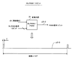
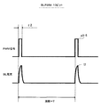
図6では、10ビットのBLPWM信号に対する、変換出力後のPWM信号p3−5と、PWM信号p3−5にもとづき、BLドライバによって生成されるBL電流I2との波形を示している。 FIG. 6 shows the waveforms of the PWM signal p3-5 after conversion output and the BL current I2 generated by the BL driver based on the PWM signal p3-5 with respect to the 10-bit BLPWM signal.
10ビットのBLPWM信号に対して、PWM信号p3−5も図5のPWM信号p3−4と同じ周期Tにする。このとき、PWM信号p3−5の1ビット変化に要する時間は、1/1024時間であるので、PWM信号p3−5のパルス幅は、PWM信号p3−4のパルス幅=τ1よりも狭いτ2(<τ1)となっている。 For the 10-bit BLPWM signal, the PWM signal p3-5 has the same period T as the PWM signal p3-4 in FIG. At this time, since the time required for 1-bit change of the PWM signal p3-5 is 1/1024 hours, the pulse width of the PWM signal p3-5 is τ2 (which is narrower than the pulse width of the PWM signal p3-4 = τ1). <Τ1).
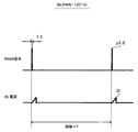
図7では、12ビットのBLPWM信号に対する、変換出力後のPWM信号p3−6と、PWM信号p3−6にもとづき、BLドライバによって生成されるBL電流I3との波形を示している。 FIG. 7 shows a waveform of a PWM signal p3-6 after conversion output with respect to a 12-bit BLPWM signal and a BL current I3 generated by the BL driver based on the PWM signal p3-6.
12ビットのBLPWM信号に対して、PWM信号p3−6も図5のPWM信号p3−4と同じ周期Tにする。このとき、PWM信号p3−6の1ビット変化に要する時間は、1/4096時間であるので、PWM信号p3−6のパルス幅は、PWM信号p3−4のパルス幅=τ1およびPWM信号p3−5のパルス幅=τ2よりも狭いτ3(<τ2<τ1)となっている。 For the 12-bit BLPWM signal, the PWM signal p3-6 also has the same period T as the PWM signal p3-4 in FIG. At this time, since the time required for 1-bit change of the PWM signal p3-6 is 1/496 hours, the pulse width of the PWM signal p3-6 is equal to the pulse width of the PWM signal p3-4 = τ1 and the PWM signal p3−3. The pulse width of 5 is τ3 (<τ2 <τ1) narrower than τ2.
ここで、図6に示すPWM信号p3−5のHレベルのパルス幅=τ2と、図7に示すPWM信号p3−6のHレベルのパルス幅=τ3とは、BLドライバが応答することができる所定値以下のパルス幅とする。 Here, the H level pulse width = τ2 of the PWM signal p3-5 shown in FIG. 6 and the H level pulse width = τ3 of the PWM signal p3-6 shown in FIG. 7 can be responded by the BL driver. The pulse width is a predetermined value or less.
この場合、パルス幅=τ2のPWM信号p3−5がBLドライバに入力しても、BLドライバは、PWM信号p3−5に正常に応答することができないので、バックライトを駆動するに必要なBL電流を生成することができない。 In this case, even if the PWM signal p3-5 having the pulse width = τ2 is input to the BL driver, the BL driver cannot normally respond to the PWM signal p3-5. The current cannot be generated.
同様に、パルス幅=τ3のPWM信号p3−6がBLドライバに入力しても、BLドライバは、PWM信号p3−6に正常に応答することができないので、バックライトを駆動するに必要なBL電流を生成することができない。 Similarly, even if the PWM signal p3-6 having the pulse width = τ3 is input to the BL driver, the BL driver cannot normally respond to the PWM signal p3-6, so that the BL necessary for driving the backlight is required. The current cannot be generated.
なぜなら、BLドライバに入力するPWM信号のパルス幅が所定値以下であると、PWM信号の立ち上がりに追従してBL電流が立ち上がる際に、BL電流の立ち上がりが十分に確保される前にPWM信号がLレベルになってしまい、PWM信号が表す情報をBL電流の電流量に反映できないからである。 This is because when the pulse width of the PWM signal input to the BL driver is equal to or smaller than a predetermined value, the PWM signal rises before the BL current rise is sufficiently secured when the BL current rises following the rise of the PWM signal. This is because the information represented by the PWM signal cannot be reflected in the current amount of the BL current.
このように、BLPWM信号のビット数を増やして、バックライトの輝度を細かく制御する場合に、1ビット当たりのPWM信号のパルス幅が所定値以下まで狭くなってしまう。PWM信号のパルス幅が狭くなると、BLドライバが正常に応答できず、輝度のリニアリティが保てなくなってしまう。また、輝度のリニアリティが保てないと、結果的に画品位の低下を引き起こすことになる。 As described above, when the number of bits of the BLPWM signal is increased to finely control the luminance of the backlight, the pulse width of the PWM signal per bit is narrowed to a predetermined value or less. When the pulse width of the PWM signal is narrowed, the BL driver cannot respond normally and the luminance linearity cannot be maintained. Further, if the luminance linearity cannot be maintained, as a result, the image quality is lowered.
本技術はこのような点に鑑みてなされたものであり、バックライトの高精度な輝度制御を実現し、画品位低下の改善を図った照明制御を行うものである。 The present technology has been made in view of such a point, and realizes high-precision luminance control of a backlight and performs illumination control with the aim of improving image quality degradation.
次に本技術の照明装置1について以降詳しく説明する。照明装置1の時分割制御部1aでは、BLPWM信号のビット数が増えても、PWM信号の分解能はそのままにし、その代わりに時間方向にPWM信号を変化させて、BLPWM信号のビット数の増加分を表現させる(以下、時分割制御部1aで行われる制御をBLPWM時分割制御とも呼ぶ)。
Next, the
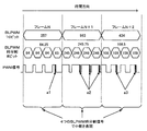
図8はBLPWM時分割制御の概念を説明するための図である。BLPWM信号は、10ビットのパラレル信号とする。なお、図中の“BLPWM10ビット”は、図1の輝度制御信号P1に該当する。
FIG. 8 is a diagram for explaining the concept of BLPWM time-division control. The BLPWM signal is a 10-bit parallel signal. The “
また、図中の“BLPWM時分割8ビット”は、図1の輝度制御信号P2に該当する。さらに、図中の“PWM信号”は、図1の輝度制御信号P3に該当する。
Further, “
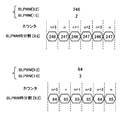
一方、フレームNでの10ビットのBLPWM信号で表現する値(輝度階調値)が257、フレームN+1での10ビットのBLPWM信号で表現する値が983、フレームN+2での10ビットのBLPWM信号で表現する値が434であったとする。 On the other hand, the value (luminance gradation value) expressed by the 10-bit BLPWM signal in frame N is 257, the value expressed by the 10-bit BLPWM signal in frame N + 1 is 983, and the 10-bit BLPWM signal in frame N + 2 Assume that the value to be expressed is 434.
このような10ビットのBLPWM信号で表現されるフレーム対して、BLPWM時分割制御として、10ビットのBLPWM信号を、例えば8ビットのBLPWM信号に変換する場合を考える。 Consider a case in which a 10-bit BLPWM signal is converted into, for example, an 8-bit BLPWM signal as BLPWM time-division control for a frame represented by such a 10-bit BLPWM signal.
この場合、10ビットの下位2ビットを切り捨てるが、これはビットシフト演算において22での割り算に相当する。フレームNに対しては、257を22で割って、64.25(=257/4)となる。64.25は、8ビットで表せる整数部分の64と、端数部分の小数点0.25とを含んでいる。
In this case, the lower 2 bits of the 10 bits are truncated, which corresponds to division by 2 2 in the bit shift operation. For frame N, 257 is divided by 2 2 to give 64.25 (= 257/4). 64.25 includes an
上記のように端数部分が生じた場合は、8ビットのBLPWM信号のうちの、少なくとも1つの整数部分を変化させることにより、10ビットのBLPWM信号を表現する。例えば、フレームNの時間領域において、10ビットのBLPWM信号の257を、8ビットのBLPWM信号の64、64、64、65というそれぞれ8ビットデータに時分割して表現する。 When a fractional part is generated as described above, a 10-bit BLPWM signal is expressed by changing at least one integer part of the 8-bit BLPWM signal. For example, in the time domain of frame N, 257 of the 10-bit BLPWM signal is time-divided into 8-bit data of 64, 64, 64, and 65 of the 8-bit BLPWM signal.
このときの8ビットBLPWM信号の平均値は、(64+64+64+65)/4=64.25となっており、4つの64、64、64、65というそれぞれ8ビットのBLPWM時分割信号によって小数を表現している。 The average value of the 8-bit BLPWM signal at this time is (64 + 64 + 64 + 65) /4=64.25, and the decimal is expressed by four 64-, 64-, 64-, and 64-bit 8-bit BLPWM time-division signals. Yes.
そして、64、65というそれぞれの値に応じたパルス幅を持つ、1ビットのPWM信号が生成される。図中の斜線部a1は、64に対して1が加算された65という値の1ビット増加分を表している。 Then, a 1-bit PWM signal having a pulse width corresponding to each value of 64 and 65 is generated. A hatched portion a1 in the figure represents a 1-bit increment of a value of 65 obtained by adding 1 to 64.
なお、65という8ビットデータの値は、図8ではフレームNの時間帯の先頭から4番目に位置しているが、フレームNの時間帯の中のどの位置にきてもよい。ただし、例えば、フレームNの時間帯の4番目に位置させるとしたら、フレーム切替時において、フレームNの時間帯では、4番目の位置に固定的に65がくるようにする。 Note that the value of 8-bit data of 65 is located at the fourth position from the beginning of the time zone of frame N in FIG. 8, but may be located at any position in the time zone of frame N. However, for example, if it is positioned at the fourth position in the time slot of frame N, 65 is fixedly positioned at the fourth position in the time slot of frame N at the time of frame switching.
一方、フレームN+1に対しては、983を22で割って、245.75(=983/4)を求める。245.75は、8ビットで表せる整数部分の245と、端数部分の小数点0.75とを含んでいる。
On the other hand, for frame N + 1, 983 is divided by 2 2 to obtain 245.75 (= 983/4). 245.75 includes an
したがって、フレームN+1の時間帯において、10ビットのBLPWM信号の983を、8ビットのBLPWM信号の245、246、246、246というそれぞれ8ビットデータに時分割して表現する。
Accordingly, 983 of the 10-bit BLPWM signal is time-divided into 8-
このときの8ビットBLPWM信号の平均値は、(245+246+246+246)/4=245.75となっており、4つの245、246、246、246というそれぞれ8ビットのBLPWM時分割信号によって小数を表現している。 The average value of the 8-bit BLPWM signal at this time is (245 + 246 + 246 + 246) /4=245.75, and the decimals are expressed by four 8-bit BLPWM time-division signals of 245, 246, 246, and 246, respectively. Yes.
そして、245、246というそれぞれの値に応じたパルス幅を持つ、1ビットのPWM信号が生成される。図中の斜線部a2は、245に対して1が加算された246という値の1ビット増加分を表している。 Then, a 1-bit PWM signal having a pulse width corresponding to each value of 245 and 246 is generated. A hatched portion a2 in the figure represents a 1-bit increment of a value of 246 obtained by adding 1 to 245.
なお、246という8ビットデータの値は、図8ではフレームN+1の時間帯の先頭から2、3、4番目に位置しているが、フレームN+1の時間帯の中のどの位置にきてもよい。ただし、例えば、フレームN+1の時間帯の2、3、4番目に位置させるとしたら、フレーム切替時において、フレームN+1の時間帯では、2、3、4番目の位置に固定的に246がくるようにする。 Note that the 8-bit data value of 246 is located at the second, third, and fourth positions from the beginning of the time slot of frame N + 1 in FIG. 8, but may be at any position in the time slot of frame N + 1. . However, for example, if it is positioned at the second, third, and fourth positions in the time slot of frame N + 1, 246 is fixedly placed at the second, third, and fourth positions in the time slot of frame N + 1 when switching frames. To.
同様に、フレームN+2に対しては、434を22で割って、108.5(=434/4)を求める。108.5は、8ビットで表せる整数部分108と、端数部分の小数点0.5とを含んでいる。
Similarly, for frame N + 2, 434 is divided by 2 2 to obtain 108.5 (= 434/4). 108.5 includes an
したがって、フレームN+2の時間帯において、10ビットのBLPWM信号の434を、8ビットのBLPWM信号の108、109、108、109というそれぞれ8ビットデータに時分割して表現する。
Therefore, the 10-
このときの8ビットBLPWM信号の平均値は、(108+109+108+109)/4=108.5となっており、4つの108、109、108、109というそれぞれ8ビットのBLPWM時分割信号によって小数を表現している。 The average value of the 8-bit BLPWM signal at this time is (108 + 109 + 108 + 109) /4=108.5, and the decimal is expressed by four 8-bit BLPWM time-division signals of 108, 109, 108, and 109, respectively. Yes.
そして、108、109というそれぞれの値に応じたパルス幅を持つ、1ビットのPWM信号が生成される。図中の斜線部a3は、108に対して1が加算された109という値の1ビット増加分を表している。
Then, a 1-bit PWM signal having a pulse width corresponding to the
なお、109という8ビットデータの値は、図8ではフレームN+2の時間帯の先頭から2、4番目に位置しているが、フレームN+2の時間帯の中のどの位置にきてもよい。ただし、例えば、フレームN+2の時間帯の2、4番目に位置させるとしたら、フレーム切替時において、フレームN+2の時間帯では、2、4番目の位置に固定的に109がくるようにする。 The 8-bit data value 109 is located at the second and fourth positions from the beginning of the time slot of frame N + 2 in FIG. 8, but may be at any position in the time slot of frame N + 2. However, for example, if it is positioned at the second and fourth positions in the time slot of the frame N + 2, 109 is fixedly placed at the second and fourth positions in the time slot of the frame N + 2 at the time of frame switching.
以上説明したように、照明装置1の時分割制御部1aは、BLPWM信号のパラレルビット数をKビット、BLPWM時分割信号のビット数をL(<K)とした場合、BLPWM信号の所定の時間領域(例えば、1フレームの時間領域)から2K-L個の分割領域を生成する。K=10、L=8とすれば、4(=210-8)つの分割領域が生成される。
As described above, the time
そして、Kビットで表現される輝度階調の値を2K-Lで除算する(10ビットで表現される。例えば、257を210-8で除算)。 Then, the luminance gradation value expressed in K bits is divided by 2 KL (expressed in 10 bits. For example, 257 is divided by 2 10-8 ).
そして、2K-L個の分割領域に対して、Lビットで表せる整数値を割り当てる。この場合、2K-L個の分割領域に割り振られた値の総和を2K-Lで割った平均値が、除算の結果の値となるように割り当てることになる。端数部分は、分割領域のうちの1つに割り当てる。例えば、64、64、64、65の総和を210-8で徐算すれば、257/210-8となるので、4つの分割領域には、64、64、64、65が割り当てられることになる。 An integer value that can be expressed by L bits is assigned to 2 KL divided regions. In this case, the average value obtained by dividing the sum of the values assigned to the 2 KL divided areas by 2 KL is assigned so as to be the value of the division result. The fractional part is assigned to one of the divided areas. For example, if the sum of 64, 64, 64, and 65 is gradually subtracted by 2 10-8 , it becomes 257/2 10-8 , so that 64, 64, 64, and 65 are assigned to the four divided areas. become.
なお、上記の図8では、各フレームに対するBLPWM時分割制御として、例えば、10ビットのBLPWM信号を時間方向に8ビットデータに時分割し、そのとき生成されたBLPWM時分割信号の8ビットデータそれぞれを1ビットのPWM信号に変換している。 In FIG. 8 described above, as BLPWM time division control for each frame, for example, a 10-bit BLPWM signal is time-divided into 8-bit data in the time direction, and the 8-bit data of the BLPWM time-division signal generated at that time is respectively Is converted into a 1-bit PWM signal.
これにより、高精度の輝度制御を実行することが可能となる。また、BLPWM信号をPWM信号に変換する場合に、BLPWM信号のパラレルビット数の違いにおいても、PWM信号の1周期を同じに維持でき、輝度のちらつきを抑制することが可能になる。 Thereby, it is possible to execute high-precision brightness control. Further, when the BLPWM signal is converted into the PWM signal, even if the number of parallel bits of the BLPWM signal is different, one cycle of the PWM signal can be maintained to be the same, and luminance flicker can be suppressed.
さらに、PWM信号の1周期を維持しても、1ビット当たりのPWM信号の変化幅は同じになるため、図1の駆動部1bに該当するBLドライバが正常に応答することができ、輝度のリニアリティを確保することが可能になる。
Further, even if one cycle of the PWM signal is maintained, the change width of the PWM signal per bit is the same, so that the BL driver corresponding to the
次に10ビットのBLPWM信号を8ビットのBLPWM時分割信号で表現する場合についてさらに詳しく説明する。なお、以降では、ビット表現を[MSB:LSB]で表す。MSB(Most Significant Bit)は最上位ビット、LSB(Least Significant Bit)は最下位ビットである。 Next, a case where a 10-bit BLPWM signal is expressed by an 8-bit BLPWM time division signal will be described in more detail. Hereinafter, the bit representation is represented by [MSB: LSB]. MSB (Most Significant Bit) is the most significant bit, and LSB (Least Significant Bit) is the least significant bit.
例えば、A信号[9:0]とは、A信号は、最下位ビットが0ビットで、最上位ビットが9ビットであり、0ビット目から9ビット目までの全部で10ビットの信号であることを表す。 For example, the A signal [9: 0] is a 10-bit signal in which the least significant bit is 0 bit, the most significant bit is 9 bits, and the 0th to 9th bits are in total. Represents that.
また、例えば、B信号[9:2]とは、B信号は、最下位ビットが2ビットで、最上位ビットが9ビットであり、2ビット目から9ビット目までの全部で8ビットの信号であることを表す。 For example, the B signal [9: 2] means that the B signal has 2 bits as the least significant bit and 9 bits as the most significant bit, and is a signal of 8 bits in total from the 2nd bit to the 9th bit. It represents that.
このような表記において以降では、10ビットパラレルのBLPWM信号をBLPWM[9:0]と表記する。さらに、BLPWM信号の2ビット目〜9ビット目までの8ビットの整数部分をBLPWM[9:2]と表記する。 In the following description, the 10-bit parallel BLPWM signal is expressed as BLPWM [9: 0]. Further, an 8-bit integer part from the second bit to the ninth bit of the BLPWM signal is expressed as BLPWM [9: 2].
さらにまた、BLPWM信号の0ビット目〜1ビット目までの2ビットの小数部分をBLPWM[1:0]と表記する。さらに、8ビットのBLPWM時分割信号をBLPWM時分割[9:2]と表記する。 Furthermore, the 2-bit decimal part from the 0th bit to the 1st bit of the BLPWM signal is expressed as BLPWM [1: 0]. Further, the 8-bit BLPWM time division signal is expressed as BLPWM time division [9: 2].
なお、小数点部分の2ビットは、0.00(10)を00(2)、0.25(10)を01(2)、0.5(10)を10(2)、0.75(10)を11(2)にそれぞれ対応させることができる。したがって、小数0.00は、BLPWM[1:0]=0と表記する(00(2)→0)。 Note that the 2 bits of the decimal part are 0.00 (10) 00 (2) , 0.25 (10) 01 (2) , 0.5 (10) 10 (2) , 0.75 (10 ) Can correspond to 11 (2) , respectively. Therefore, the decimal number 0.00 is expressed as BLPWM [1: 0] = 0 (00 (2) → 0).
また、小数0.25は、BLPWM[1:0]=1と表記する(01(2)→1)。同様に、小数0.50は、BLPWM[1:0]=2と表記し(10(2)→2)、小数0.75は、BLPWM[1:0]=3と表記する(11(2)→3)。 The decimal number 0.25 is expressed as BLPWM [1: 0] = 1 (01 (2) → 1). Similarly, the decimal 0.50 is expressed as BLPWM [1: 0] = 2 (10 (2) → 2), and the decimal 0.75 is expressed as BLPWM [1: 0] = 3 (11 (2 ) → 3).
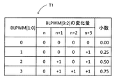
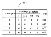
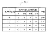
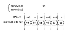
図9はBLPWM[9:2]の変化量を示す図である。テーブルT1は、BLPWM[1:0]と、BLPWM[9:2]の変化量と、小数との項目を有する。なお、BLPWM[9:2]の変化量は、n、n+1、n+2、n+3の4つの時間領域に分割されており、n、n+1、n+2、n+3は、カウンタのカウント値に相当する。 FIG. 9 is a diagram showing the amount of change in BLPWM [9: 2]. The table T1 includes items of BLPWM [1: 0], BLPWM [9: 2] change amount, and decimal. The amount of change in BLPWM [9: 2] is divided into four time regions, n, n + 1, n + 2, and n + 3, and n, n + 1, n + 2, and n + 3 correspond to the count value of the counter.
また、1フレーム内おいて、このカウンタは、n→n+1→n+2→n+3→n→n+1→・・・と巡回カウントを行うものとする。 Also, within one frame, this counter performs cyclic counting in the order of n → n + 1 → n + 2 → n + 3 → n → n + 1 →.
テーブルT1において、BLPWM[1:0]=0は、小数0.00を表し、BLPWM[9:2]の変化量における、カウントn、n+1、n+2、n+3はすべて“0”となる。なお、“0”とは、BLPWM[9:2]の2ビット〜9ビットまでの8ビットデータで表現されるそのままの値が用いられるということである。 In the table T1, BLPWM [1: 0] = 0 represents a decimal number 0.00, and the counts n, n + 1, n + 2, and n + 3 in the variation amount of BLPWM [9: 2] are all “0”. Note that “0” means that the same value represented by 8-bit data from 2 bits to 9 bits of BLPWM [9: 2] is used.
例えば、BLPWM[9:0]で表現する値が256ならば、256/4=64となって小数は含まれない。したがって、1フレーム内のカウントn、n+1、n+2、n+3のすべての時間領域の値は、8ビットデータの整数(=64)で表現できるので、この場合、カウントn、n+1、n+2、n+3はすべて“0”となる。 For example, if the value expressed by BLPWM [9: 0] is 256, 256/4 = 64 and no decimals are included. Therefore, all the time domain values of the counts n, n + 1, n + 2, and n + 3 in one frame can be expressed by integers (= 64) of 8-bit data. In this case, the counts n, n + 1, n + 2, and n + 3 are all It becomes “0”.
また、BLPWM[1:0]=1は、小数0.25を表し、BLPWM[9:2]の変化量における、カウントn、n+1、n+2、n+3のいずれか1つは“+1”となり、残り3つは“0”となる。 BLPWM [1: 0] = 1 represents a decimal number of 0.25, and any one of the counts n, n + 1, n + 2, n + 3 in the amount of change in BLPWM [9: 2] is “+1”, and the rest Three become “0”.
なお、“+1”とは、BLPWM[1:0]の0ビット〜1ビットまでの2ビットデータでの小数の表現を意味している。 Note that “+1” means a decimal representation of 2-bit data from 0 to 1 bit of BLPWM [1: 0].
例えば、BLPWM[9:0]で表現する値が257ならば、257/4=64.25となって小数0.25を含んでいる。64.25は、64、64、64、65(=64+1)の平均で表せるので、4つの時間領域の内の3つが“0”となって64を表現し、4つの時間領域の内の1つが“+1”となって65を表現するものである。 For example, if the value expressed by BLPWM [9: 0] is 257, 257/4 = 64.25, which includes the decimal number 0.25. 64.25 can be represented by the average of 64, 64, 64, 65 (= 64 + 1), so three of the four time domains represent “0” to represent 64, and 1 of the four time domains One becomes “+1” and expresses 65.
図9の例では、BLPWM[1:0]=1の場合、カウントn、n+1、n+2の3つの時間領域が“0”、カウントn+3の1つの時間領域が“1”となるように設定されている。 In the example of FIG. 9, when BLPWM [1: 0] = 1, the three time regions of counts n, n + 1, and n + 2 are set to “0”, and one time region of count n + 3 is set to “1”. ing.
さらに、BLPWM[1:0]=2は、小数0.50を表し、BLPWM[9:2]の変化量における、カウントn、n+1、n+2、n+3のいずれか2つは“+1”となり、残り2つは“0”となる。 Further, BLPWM [1: 0] = 2 represents a decimal number 0.50, and any two of the counts n, n + 1, n + 2, n + 3 in the amount of change in BLPWM [9: 2] are “+1”, and the rest Two become “0”.
例えば、BLPWM[9:0]で表現する値が434ならば、434/4=108.5となって小数0.5を含んでいる。108.5は、108、108、109(=108+1)、109(=108+1)の平均で表せるので、4つの時間領域の内の2つが“0”となって108を表現し、4つの時間領域の内の2つが“+1”となって109を表現するものである。 For example, if the value expressed by BLPWM [9: 0] is 434, 434/4 = 108.5, which includes the decimal number 0.5. Since 108.5 can be represented by the average of 108, 108, 109 (= 108 + 1), 109 (= 108 + 1), two of the four time domains represent “0” to represent 108 and represent four time domains. Two of these become “+1” to represent 109.
図9の例では、BLPWM[1:0]=2の場合、カウントn、n+2の2つの時間領域が“0”、カウントn+1、n+3の2つの時間領域が“+1”となるように設定されている。 In the example of FIG. 9, when BLPWM [1: 0] = 2, the two time regions of count n and n + 2 are set to “0”, and the two time regions of count n + 1 and n + 3 are set to “+1”. ing.
さらにまた、BLPWM[1:0]=3は、小数0.75を表し、BLPWM[9:2]の変化量における、カウントn、n+1、n+2、n+3のいずれか3つは“+1”となり、残り1つは“0”となる。 Furthermore, BLPWM [1: 0] = 3 represents a decimal number 0.75, and any three of the counts n, n + 1, n + 2, n + 3 in the amount of change in BLPWM [9: 2] are “+1”. The remaining one is “0”.
例えば、BLPWM[9:0]で表現する値が983ならば、983/4=245.75となって小数0.75を含んでいる。245.75は、245、246(=245+1)、246(=245+1)、246(=245+1)の平均で表せるので、4つの時間領域の内の1つが“0”となって245を表現し、4つの時間領域の内の3つが“+1”となって246を表現するものである。 For example, if the value expressed by BLPWM [9: 0] is 983, 983/4 = 245.75, which includes the decimal number 0.75. 245.75 can be expressed as an average of 245, 246 (= 245 + 1), 246 (= 245 + 1), and 246 (= 245 + 1), so that one of the four time domains becomes “0” to express 245, Three of the four time domains become “+1” to represent 246.
図9の例では、BLPWM[1:0]=3の場合、カウントnの1つの時間領域が“0”、カウントn+1、n+2、n+3の3つの時間領域が“1”となるように設定されている。なお、変化量の他バージョンについては後述する。 In the example of FIG. 9, when BLPWM [1: 0] = 3, one time region of count n is set to “0”, and three time regions of counts n + 1, n + 2, and n + 3 are set to “1”. ing. The other version of the change amount will be described later.
図10、図11はBLPWM時分割制御の一例を示す図である。10ビット→8ビットのBLPWM時分割制御の例を示す。フレームNでのBLPWM[9:0]で表現する値が1024、フレームN+1でのBLPWM[9:0]で表現する値が259、フレームN+2でのBLPWM[9:0]で表現する値が986とする。 10 and 11 are diagrams illustrating an example of BLPWM time division control. An example of 10-bit → 8-bit BLPWM time division control is shown. The value expressed by BLPWM [9: 0] in frame N is 1024, the value expressed by BLPWM [9: 0] in frame N + 1 is 259, and the value expressed by BLPWM [9: 0] in frame N + 2 is 986. And
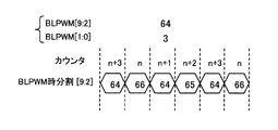
フレームNについては、256(=1024/4)なので、BLPWM[9:2]=256であり、BLPWM[1:0]=0(小数0.00に該当)となる。 Since frame N is 256 (= 1024/4), BLPWM [9: 2] = 256, and BLPWM [1: 0] = 0 (corresponding to decimal 0.00).
また、フレームN+1については、64.75(=259/4)なので、BLPWM[9:2]=64であり、BLPWM[1:0]=3(小数0.75に該当)となる。 For frame N + 1, since it is 64.75 (= 259/4), BLPWM [9: 2] = 64 and BLPWM [1: 0] = 3 (corresponding to the decimal number 0.75).
さらに、フレームN+2については、246.5(=986/4)なので、BLPWM[9:2]=246であり、BLPWM[1:0]=2(小数0.50に該当)となる。 Furthermore, since the frame N + 2 is 246.5 (= 986/4), BLPWM [9: 2] = 246 and BLPWM [1: 0] = 2 (corresponding to the decimal 0.50).
BLPWM時分割[9:2]について見ると、図10において、フレームNでは、BLPWM[1:0]=0なので、テーブルT1にもとづき、カウントn、n+1、n+2、n+3の時間領域はすべて“0”である。 Looking at BLPWM time division [9: 2], in FIG. 10, in frame N, BLPWM [1: 0] = 0, so that the time domain of counts n, n + 1, n + 2, and n + 3 are all “0” based on table T1. ".
したがって、フレームNのBLPWM時分割[9:2]は、カウントn、n+1、n+2、n+3の時間領域において、すべて256というそれぞれ8ビットデータになる。そして、256という値に応じたパルス幅を持つ、1ビットのPWM信号が生成されることになる。 Therefore, BLPWM time division [9: 2] of frame N is all 8-bit data of 256 in the time domain of counts n, n + 1, n + 2, and n + 3. Then, a 1-bit PWM signal having a pulse width corresponding to a value of 256 is generated.
一方、図11において、フレームN+1では、BLPWM[1:0]=3なので、テーブルT1にもとづき、カウントnの時間領域は“0”、カウントn+1、n+2、n+3の時間領域は“+1”となる。 On the other hand, in FIG. 11, since BLPWM [1: 0] = 3 in frame N + 1, the time domain of count n is “0” and the time domain of counts n + 1, n + 2, and n + 3 is “+1” based on table T1. .
したがって、フレームN+1のBLPWM時分割[9:2]は、カウントnの時間領域の値は64、カウントn+1、n+2、n+3の時間領域は65となる。そして、64、65というそれぞれの値に応じたパルス幅を持つ、1ビットのPWM信号が生成されることになる。 Therefore, in the BLPWM time division [9: 2] of the frame N + 1, the time domain value of the count n is 64, and the time domain of the counts n + 1, n + 2, and n + 3 is 65. Then, a 1-bit PWM signal having a pulse width corresponding to each value of 64 and 65 is generated.
さらに、図11において、フレームN+2では、BLPWM[1:0]=2なので、テーブルT1にもとづき、カウントn、n+2の時間領域は“0”、カウントn+1、n+3の時間領域は“+1”となる。 Further, in FIG. 11, in frame N + 2, BLPWM [1: 0] = 2, so that the time domain of count n and n + 2 is “0” and the time domain of count n + 1 and n + 3 is “+1” based on table T1. .
したがって、フレームN+2のBLPWM時分割[9:2]は、カウントn、n+2の時間領域の値は246、カウントn+1、n+3の時間領域は247となる。そして、246、247というそれぞれの値に応じたパルス幅を持つ、1ビットのPWM信号が生成されることになる。 Therefore, in the BLPWM time division [9: 2] of the frame N + 2, the time domain value of the count n and n + 2 is 246, and the time domain of the count n + 1 and n + 3 is 247. Then, a 1-bit PWM signal having a pulse width corresponding to each value of 246 and 247 is generated.
上記のようなBLPWM時分割制御を行うことにより、BLドライバが正常に応答できるPWM信号の最小のパルス幅を維持することができ、さらにPWM信号の周期も維持することが可能になる。 By performing BLPWM time division control as described above, it is possible to maintain the minimum pulse width of the PWM signal to which the BL driver can normally respond, and also to maintain the period of the PWM signal.
なお、図9で示したテーブルT1では、BLPWM[1:0]=1のとき、カウントn+3の時間領域を“+1”としている。さらに、PWM[1:0]=2のとき、カウントn+1、n+3の時間領域を“+1”とし、BLPWM[1:0]=3のとき、カウントn+1、n+2、n+3の時間領域を“+1”としている。 In the table T1 shown in FIG. 9, when BLPWM [1: 0] = 1, the time region of the count n + 3 is set to “+1”. Further, when PWM [1: 0] = 2, the time region of count n + 1, n + 3 is “+1”, and when BLPWM [1: 0] = 3, the time region of count n + 1, n + 2, n + 3 is “+1”. It is said.
テーブルT1は一例であって、上記の変化量の“+1”とする位置は、分散して設定し、またその設定位置は、任意に変更可能である。 The table T1 is an example, and the positions where the change amount is “+1” are set in a distributed manner, and the set positions can be arbitrarily changed.
次にBLPWM[9:2]の変化量の他のバージョンについて説明する。図12はBLPWM[9:2]の変化量の他のバージョンを示す図である。図12のテーブルT1−1は、“+1”とする設定箇所の異なるバージョンを示している。 Next, another version of the amount of change in BLPWM [9: 2] will be described. FIG. 12 is a diagram showing another version of the amount of change in BLPWM [9: 2]. A table T1-1 in FIG. 12 shows different versions of the set location set to “+1”.
テーブルT1−1の端数部分の表現において、BLPWM[1:0]=1のとき、カウントnの時間領域を“+1”とし、BLPWM[1:0]=2のとき、カウントn、n+2の時間領域を“+1”としている。また、BLPWM[1:0]=3のとき、カウントn、n+1、n+2の時間領域を“+1”としている。 In the representation of the fractional part of the table T1-1, when BLPWM [1: 0] = 1, the time region of the count n is “+1”, and when BLPWM [1: 0] = 2, the time of the count n and n + 2 The area is set to “+1”. Further, when BLPWM [1: 0] = 3, the time regions of the counts n, n + 1, and n + 2 are set to “+1”.
図13はBLPWM時分割を示す図である。テーブルT1−1に対応したBLPWM時分割[9:2]=246、BLPWM[1:0]=2の場合と、BLPWM時分割[9:2]=64、BLPWM[1:0]=3の場合とを示す。 FIG. 13 shows BLPWM time division. BLPWM time division [9: 2] = 246, BLPWM [1: 0] = 2 corresponding to table T1-1, BLPWM time division [9: 2] = 64, BLPWM [1: 0] = 3 Indicates the case.
BLPWM[9:2]=246で、BLPWM[1:0]=2の場合、テーブルT1−1では、カウントn、n+2の時間領域が“+1”、カウントn+1、n+3の時間領域が“0”となっている。 When BLPWM [9: 2] = 246 and BLPWM [1: 0] = 2, in the table T1-1, the time region of the count n and n + 2 is “+1”, and the time region of the count n + 1 and n + 3 is “0”. It has become.
したがって、このときのBLPWM時分割[9:2]は、カウントn、n+2の時間領域に247が位置し、カウントn+1、n+3の時間領域に246が位置することになる。
Accordingly, in this BLPWM time division [9: 2], 247 is located in the time region of count n, n + 2, and 246 is located in the time region of count n + 1,
また、BLPWM[9:2]=64で、BLPWM[1:0]=3の場合、テーブルT1−1では、カウントn、n+1、n+2の時間領域が“+1”、カウントn+3の時間領域が“0”となっている。 Further, when BLPWM [9: 2] = 64 and BLPWM [1: 0] = 3, in the table T1-1, the time region of the count n, n + 1, n + 2 is “+1”, and the time region of the count n + 3 is “ 0 ”.
したがって、このときのBLPWM時分割[9:2]は、カウントn、n+1、n+2の時間領域に65(=64+1)が位置し、カウントn+3の時間領域に64(=64+0)が位置することになる。
Therefore, in this BLPWM time division [9: 2], 65 (= 64 + 1) is located in the time domain of counts n, n + 1, and n + 2, and 64 (= 64 + 0) is located in the time domain of
図14はBLPWM[9:2]の変化量の他のバージョンを示す図である。図9のテーブルT1では、BLPWM[9:2]の変化量を“+1”としたが、図14のテーブルT1−2では、“+1”に加えて、さらに“+2”の変化量も設定して、端数部分を表現している。 FIG. 14 is a diagram showing another version of the amount of change in BLPWM [9: 2]. In the table T1 of FIG. 9, the change amount of BLPWM [9: 2] is “+1”, but in the table T1-2 of FIG. 14, in addition to “+1”, a change amount of “+2” is also set. The fractional part is expressed.
テーブルT1−2の端数部分の表現において、BLPWM[1:0]=1のとき、カウントnの時間領域を“+1”とし、BLPWM[1:0]=2のとき、カウントn、n+2の時間領域を“+1”としている。また、BLPWM[1:0]=3のとき、カウントnの時間領域を“+2”、カウントn+2の時間領域を“+1”としている。 In the expression of the fractional part of the table T1-2, when BLPWM [1: 0] = 1, the time region of the count n is “+1”, and when BLPWM [1: 0] = 2, the time of the count n and n + 2 The area is set to “+1”. When BLPWM [1: 0] = 3, the time region of count n is “+2”, and the time region of count n + 2 is “+1”.
図15はBLPWM時分割を示す図である。テーブルT1−2に対応したBLPWM時分割[9:2]=64、BLPWM[1:0]=3の場合を示す。 FIG. 15 shows BLPWM time division. The case where BLPWM time division [9: 2] = 64 and BLPWM [1: 0] = 3 corresponding to the table T1-2 is shown.
BLPWM[9:2]=64で、BLPWM[1:0]=3の場合、テーブルT1−2では、カウントnの時間領域を“+2”、カウントn+1、n+3の時間領域を“0”カウントn+2の時間領域を“+1”としている。 When BLPWM [9: 2] = 64 and BLPWM [1: 0] = 3, in the table T1-2, the time region of count n is “+2”, the time region of count n + 1, n + 3 is “0”, and count n + 2. Is set to “+1”.
したがって、このときのBLPWM時分割[9:2]は、カウントnの時間領域に66(=64+2)が位置し、カウントn+1、n+3の時間領域に64(=64+0)が位置し、カウントn+2の時間領域に65(=64+1)が位置することになる。 Therefore, in this BLPWM time division [9: 2], 66 (= 64 + 2) is located in the time region of count n, 64 (= 64 + 0) is located in the time region of count n + 1, n + 3, and the count n + 2 65 (= 64 + 1) is located in the time domain.
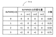
図16はBLPWM[9:2]の変化量の他のバージョンを示す図である。図9のテーブルT1では、BLPWM[9:2]の変化量を“+1”としたが、図16のテーブルT1−3では、“+1”に加えて、さらに“+2”の変化量、さらにまた“−1”の変化量も設定して、端数部分を表現している。 FIG. 16 is a diagram showing another version of the amount of change in BLPWM [9: 2]. In the table T1 of FIG. 9, the change amount of BLPWM [9: 2] is “+1”, but in the table T1-3 of FIG. 16, in addition to “+1”, the change amount of “+2” is further increased. The amount of change of “−1” is also set to express the fractional part.
テーブルT1−3の端数部分の表現において、BLPWM[1:0]=1のとき、カウントn、n+2の時間領域を“+1”とし、カウントn+3の時間領域を“−1”としている。BLPWM[1:0]=2のとき、カウントn、n+2の時間領域を“+1”としている。また、BLPWM[1:0]=3のとき、カウントnの時間領域を“+2”、カウントn+2の時間領域を“+1”としている。 In the expression of the fractional part of the table T1-3, when BLPWM [1: 0] = 1, the time region of the count n and n + 2 is “+1”, and the time region of the count n + 3 is “−1”. When BLPWM [1: 0] = 2, the time region of the count n and n + 2 is “+1”. When BLPWM [1: 0] = 3, the time region of count n is “+2”, and the time region of count n + 2 is “+1”.
図17はBLPWM時分割を示す図である。テーブルT1−3に対応したBLPWM時分割[9:2]=64、BLPWM[1:0]=1の場合を示す。 FIG. 17 shows BLPWM time division. The case of BLPWM time division [9: 2] = 64 and BLPWM [1: 0] = 1 corresponding to the table T1-3 is shown.
BLPWM[9:2]=64で、BLPWM[1:0]=1の場合、テーブルT1−3では、カウントn、n+2の時間領域を“+1”とし、カウントn+1の時間領域を“0”とし、カウントn+3の時間領域を“−1”としている。 When BLPWM [9: 2] = 64 and BLPWM [1: 0] = 1, in the table T1-3, the time region of the count n and n + 2 is “+1”, and the time region of the count n + 1 is “0”. The time region of the count n + 3 is “−1”.
したがって、このときのBLPWM時分割[9:2]は、カウントn、n+2の時間領域に65(=64+1)が位置し、カウントn+1の時間領域に64(=64+0)が位置し、カウントn+3の時間領域に63(=64−1)が位置することになる。なお、上記の変化量の設定は一例であって、上記以外のバージョンの変化量を設定することも可能である。 Therefore, in this BLPWM time division [9: 2], 65 (= 64 + 1) is located in the time region of count n, n + 2, 64 (= 64 + 0) is located in the time region of count n + 1, and the count n + 3 63 (= 64-1) is located in the time domain. Note that the above-described change amount setting is an example, and it is possible to set a change amount of a version other than the above.
次にBLPWM時分割制御の他の例として、12ビットのBLPWM信号を8ビットのBLPWM時分割信号で表現する場合について説明する。BLPWM信号は、12ビットパラレルとする。また、フレームNでの12ビットのBLPWM信号で表現する値が3163であったとする。 Next, as another example of BLPWM time division control, a case where a 12-bit BLPWM signal is expressed by an 8-bit BLPWM time division signal will be described. The BLPWM signal is assumed to be 12-bit parallel. Further, it is assumed that the value expressed by the 12-bit BLPWM signal in the frame N is 3163.
このような12ビットのBLPWM信号で表現されるフレーム対して、BLPWM時分割制御として、12ビットのBLPWM信号を例えば、8ビットのBLPWM信号に変換する場合を考える。 Consider a case where a 12-bit BLPWM signal is converted into, for example, an 8-bit BLPWM signal as BLPWM time-division control for a frame expressed by such a 12-bit BLPWM signal.
この場合、12ビットの下位4ビットを切り捨てるが、これはビットシフト演算において24での割り算に相当するので、フレームNに対しては、3163を24で割って、197.6875(=3163/16)を求める。197.6875は、8ビットで表せる整数部分の197と、端数部分の小数点0.6875を含んでいる。
In this case, the lower 4 bits of 12 bits are rounded down, which corresponds to division by 2 4 in the bit shift operation, so that for frame N, 3163 is divided by 2 4 and 197.6875 (= 3163). / 16). 196.875 includes an
したがって、フレームNの時間領域において、12ビットのBLPWM信号の3163を、8ビットのBLPWM信号の5個の197という値と、8ビットのBLPWM信号の11個の198という値とに時分割する。 Therefore, in the time domain of frame N, 3163 of the 12-bit BLPWM signal is time-divided into 5 values of 197 of the 8-bit BLPWM signal and 11 values of 198 of the 8-bit BLPWM signal.
このときの8ビットBLPWM信号の平均値は、(197×5+198×11)/16=197.6875となっており、5個の197と、11個の198というそれぞれ8ビットのBLPWM時分割制御信号によって小数を表現している。 The average value of the 8-bit BLPWM signal at this time is (197 × 5 + 198 × 11) /16=1977.6875, and the 5-bit BLPWM time-division control signal of 5 197 and 11 198, respectively. Represents a decimal.
図18はBLPWM[11:4]の変化量を示す図である。テーブルT2は、BLPWM[3:0]と、BLPWM[11:4]の変化量と、小数との項目を有する。 FIG. 18 is a diagram illustrating the amount of change in BLPWM [11: 4]. The table T2 includes items of BLPWM [3: 0], BLPWM [11: 4] change amounts, and decimal numbers.
なお、BLPWM[11:4]の変化量は、n、n+1、・・・、n+14、n+15の16個の時間領域に分割されており、n、n+1、・・・、n+14、n+15は、カウンタのカウント値に相当する。 The amount of change in BLPWM [11: 4] is divided into 16 time regions of n, n + 1,..., N + 14, n + 15, and n, n + 1,..., N + 14, n + 15 are counters. It corresponds to the count value.
また、1フレーム内おいて、このカウンタは、n→n+1→・・・→n+14→n+15→n→n+1→・・・と巡回カウントを行うとする。 Further, it is assumed that this counter performs a cyclic count in the order of n → n + 1 →... → n + 14 → n + 15 → n → n + 1 →.
テーブルT2の端数部分の表現として、例えば、BLPWM[3:0]=1であるならば、小数0.0625を表し、BLPWM[11:4]の変化量における、カウントn、n+1、・・・、n+14、n+15のいずれか1個は“+1”となり、残り15個は“0”となる。 As an expression of the fractional part of the table T2, for example, if BLPWM [3: 0] = 1, it represents a decimal number 0.0625 and counts n, n + 1,... In the amount of change in BLPWM [11: 4]. , N + 14, or n + 15 is “+1”, and the remaining 15 are “0”.
また、例えば、BLPWM[3:0]=11であるならば、小数0.6875を表し、BLPWM[11:4]の変化量における、カウントn、n+1、・・・、n+14、n+15のいずれか11個は“+1”となり、残り5個は“0”となる。 Further, for example, if BLPWM [3: 0] = 11, it represents a decimal number 0.6875, and any one of counts n, n + 1,..., N + 14, n + 15 in the amount of change in BLPWM [11: 4]. Eleven are "+1" and the remaining five are "0".
なお、その他のBLPWM[3:0]についても同様な考え方の設定であり、テーブルの見方は上述したので説明は省略する。 The other BLPWM [3: 0] are set in the same way of thinking, and the way of viewing the table has been described above, and the description thereof will be omitted.
図19はBLPWM時分割制御の一例を示す図である。12ビット→8ビットのBLPWM時分割制御の例を示す。フレームN+1でのBLPWM[11:0]で表現する値が3163とする。 FIG. 19 is a diagram illustrating an example of BLPWM time-division control. An example of 12-bit to 8-bit BLPWM time division control is shown. A value expressed by BLPWM [11: 0] in the frame N + 1 is 3163.
フレームN+1については、197.6875(=3163/16)なので、BLPWM[11:4]=197であり、BLPWM[3:0]=11(小数0.6875に該当)となる。 Since the frame N + 1 is 197.6875 (= 3163/16), BLPWM [11: 4] = 197 and BLPWM [3: 0] = 11 (corresponding to the decimal number 0.6875).
フレームN+1では、BLPWM[3:0]=11なので、テーブルT2にもとづき、カウントn、n+3、n+6、n+9、n+12の時間領域は“0”、カウントn+1、n+2、n+4、n+5、n+7、n+8、n+10、n+11、n+13、n+14、n+15の時間領域は“+1”となる。 In frame N + 1, since BLPWM [3: 0] = 11, the time domain of counts n, n + 3, n + 6, n + 9, and n + 12 is “0” based on table T2, and counts n + 1, n + 2, n + 4, n + 5, n + 7, n + 8, The time domain of n + 10, n + 11, n + 13, n + 14, and n + 15 is “+1”.
したがって、フレームN+1のBLPWM時分割[11:4]は、カウントn、n+3、n+6、n+9、n+12の時間領域は197(=197+0)、カウントn+1、n+2、n+4、n+5、n+7、n+8、n+10、n+11、n+13、n+14、n+15の時間領域は198(=197+1)となる。 Therefore, BLPWM time division [11: 4] of frame N + 1 has a time domain of counts n, n + 3, n + 6, n + 9, and n + 12 is 197 (= 197 + 0), counts n + 1, n + 2, n + 4, n + 5, n + 7, n + 8, n + 10, The time domain of n + 11, n + 13, n + 14, and n + 15 is 198 (= 197 + 1).
そして、197、198というそれぞれの値に応じたパルス幅を持つ、1ビットのPWM信号が生成されることになる。 Then, a 1-bit PWM signal having a pulse width corresponding to each value of 197 and 198 is generated.
図20はBLPWM[11:4]の変化量の他のバージョンを示す図である。図18のテーブルT2では、BLPWM[11:4]の変化量を“+1”としたが、図20のテーブルT2−1では、“+1”に加えて、さらに“+2”の変化量も設定して、端数部分を表現している。なお、テーブルの見方については詳述したので説明は省略する。 FIG. 20 is a diagram showing another version of the amount of change in BLPWM [11: 4]. In table T2 in FIG. 18, the change amount of BLPWM [11: 4] is “+1”, but in table T2-1 in FIG. 20, in addition to “+1”, a change amount of “+2” is also set. The fractional part is expressed. In addition, since the way of looking at the table has been described in detail, the description is omitted.
次に照明装置1の他の実施の形態について説明する。図21は照明装置の構成例を示す図である。照明装置1−1は、時分割制御部1a、駆動部1b、光源1cおよび更新部1dを備える。なお、図1と同じ構成要素については説明は省略する。
Next, another embodiment of the
更新部1dは、第1のビット数の輝度制御信号P1に対し、第1のビット数で表現される輝度階調の値を更新する。この場合、輝度制御信号P3が第1の周期から第2の周期に切り替わるタイミングで、該輝度階調の値を更新する。
The updating
図22はBLPWM信号の更新タイミングを示す図である。BLPWM[9:0]は、10ビットデータの表現値が259、986、1020となっている。 FIG. 22 is a diagram showing the update timing of the BLPWM signal. BLPWM [9: 0] has 10-bit data representation values of 259, 986, and 1020.
このように、BLPWM[9:0]の輝度階調の値は更新されていくが、BLPWM[9:0]からBLPWM時分割[9:2]に変換し、BLPWM時分割[9:2]からPWM信号への生成時においては、PWM信号の周期の切り替わりタイミングで、BLPWM[9:2]の輝度階調の値を更新させる。 In this way, the brightness gradation value of BLPWM [9: 0] is updated, but the BLPWM [9: 0] is converted to BLPWM time division [9: 2] and BLPWM time division [9: 2]. In the generation from the PWM signal to the PWM signal, the brightness gradation value of BLPWM [9: 2] is updated at the timing of switching the period of the PWM signal.
例えば、PWM信号のデューティDt1の周期F1からデューティDt2の周期F2への切り替わりタイミングで、BLPWM[9:0]の輝度階調値が259から986に更新されている。 For example, the luminance gradation value of BLPWM [9: 0] is updated from 259 to 986 at the switching timing from the period F1 of the duty Dt1 of the PWM signal to the period F2 of the duty Dt2.
また、PWM信号のデューティDt2の周期F2からデューティDt3の周期F3への切り替わりタイミングで、BLPWM[9:0]の輝度階調値が986から1020に更新されている(なお、実際には、回路処理上の遅延が発生するので、PWM信号の周期の切れ目と、BLPWM[9:0]の更新タイミングとにはタイムラグが発生するが、図22は説明がわかりやすいように理想的な状態を示しているものである)。 In addition, the luminance gradation value of BLPWM [9: 0] is updated from 986 to 1020 at the switching timing of the cycle D2 of the PWM signal from the cycle F2 of the duty Dt2 to the cycle F3 of the duty Dt3. Since a processing delay occurs, a time lag occurs between the break of the PWM signal cycle and the update timing of BLPWM [9: 0]. FIG. 22 shows an ideal state for easy understanding. Is)
このような制御を行うことで、PWM信号のあるデューティからなる1周期を壊さずにPWM信号の輝度階調の値を更新されるので、バックライトの輝度のちらつきをさらに低減することが可能になる。 By performing such control, the luminance gradation value of the PWM signal is updated without destroying one cycle of a certain duty of the PWM signal, so that it is possible to further reduce the luminance flicker of the backlight. Become.
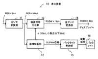
次に本発明の照明装置の機能を含む表示装置の構成について説明する。図23は表示装置の構成例を示す図である。表示回路10は、ガンマ(γ)変換部11、画像解析部12、画像信号生成部13、逆ガンマ(1/γ)変換部14、バックライト制御部15およびバックライト16を備える。
Next, the structure of the display device including the function of the lighting device of the present invention will be described. FIG. 23 is a diagram illustrating a configuration example of a display device. The
なお、図1の時分割制御部1aと駆動部1bの機能、さらに図21の更新部1dの機能は、バックライト制御部15に含まれる。また、図1の光源1cは、バックライト16に該当する。
The functions of the time
ガンマ変換部11は、R(第1の副画素)、G(第2の副画素)、B(第3の副画素)各々が例えば、8ビットの入力RGB信号をガンマ変換して、各々が16ビットのRGB信号(第1の画像信号)を出力する。 For example, each of R (first subpixel), G (second subpixel), and B (third subpixel) gamma-converts an 8-bit input RGB signal, A 16-bit RGB signal (first image signal) is output.
画像解析部12は、ガンマ変換部11から出力されたRGB信号を受信すると、伸長係数α(例えば、10ビット、小数点以下8ビット)を算出し、さらにバックライト16の輝度を制御するためのBLPWM信号(第1の輝度制御信号)を生成する。
When receiving the RGB signal output from the
画像信号生成部13は、伸長係数αにもとづいてW(第4の副画素)信号を生成して、R、G、B、W各々が例えば、16ビットのRGBW信号(第2の画像信号)を出力する。
The image
逆ガンマ変換部14は、画像信号生成部13から出力されたRGBW信号を逆ガンマ変換して、R、G、B、W各々が例えば、8ビットのRGBW信号をディスプレイ側へ出力する。
The inverse
バックライト制御部15は、画像解析部12から出力されたBLPWM信号にもとづいてバックライト16の輝度制御を行う。
The
すなわち、バックライト制御部15は、バックライト16の輝度を制御するための、第1のビット数のBLPWM信号に対して、BLPWM信号で表現される値を、第1のビット数よりも小さな第2のビット数を持つBLPWM時分割信号(第2の輝度制御信号)で時分割し、BLPWM時分割信号で表現される値に対応するパルス幅を持つPWM信号(第3の輝度制御信号)を生成する。
That is, the
そして、バックライト制御部15は、PWM信号にもとづいて、バックライト16を発光させるための駆動信号を生成して、バックライト16へ供給する。
Then, the
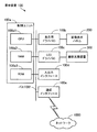
次に表示装置のハードウェア構成例について説明する。図24は表示装置のハードウェア構成例を示す図である。 Next, a hardware configuration example of the display device will be described. FIG. 24 is a diagram illustrating a hardware configuration example of the display device.
表示装置100は、制御ユニット100aと、表示用ドライバIC(Integrated Circuit)100b、LEDドライバIC100c、入出力インタフェース100d、通信インタフェース100eを含み、バス100fを介して相互に信号が入出力可能に接続されている。さらに、表示装置100は、画像表示パネル200と、面状光源装置300を含む。
The display device 100 includes a
制御ユニット100aは、CPU(Central Processing Unit:中央処理装置)100a1を含み、CPU100a1により装置全体を制御する。このような制御ユニット100aは、さらに、RAM(Random Access Memory)100a2、ROM(Read Only Memory)100a3を含み、複数の周辺機器が接続されている。
The
RAM100a2は、表示装置100の主記憶装置として使用される。RAM100a2には、CPU100a1に実行させるOS(Operating System)のプログラムやアプリケーションプログラムの少なくとも一部が一時的に格納される。また、RAM100a2には、CPU100a1による処理に必要な各種データが格納される。 The RAM 100a2 is used as a main storage device of the display device 100. The RAM 100a2 temporarily stores at least part of an OS (Operating System) program and application programs to be executed by the CPU 100a1. The RAM 100a2 stores various data necessary for processing by the CPU 100a1.
ROM100a3は、読出し専用の半導体記憶装置で、OSのプログラム、アプリケーションプログラム、及び書き替えをしない固定データが格納される。また、ROM100a3の代わり、あるいはROM100a3に加えて、二次記憶装置としてフラッシュメモリ等の半導体記憶装置を使用することもできる。 The ROM 100a3 is a read-only semiconductor storage device that stores an OS program, application programs, and fixed data that is not rewritten. Further, instead of the ROM 100a3 or in addition to the ROM 100a3, a semiconductor storage device such as a flash memory can be used as a secondary storage device.
このような制御ユニット100aには、周辺機器として、例えば、表示用ドライバIC100bと、LEDドライバIC100c、入出力インタフェース100d、通信インタフェース100eが接続されている。
For example, a
表示用ドライバIC100bは、画像表示パネル200が接続されている。表示用ドライバIC100bは、入力信号が入力されると、所定の処理を実行して、出力信号を生成する。表示用ドライバIC100bは、生成した出力信号に応じた制御信号を画像表示パネル200に出力することによって画像表示パネル200に画像を表示させる。
The
LEDドライバIC100cには、面状光源装置300に含まれるサイドライト光源の各光源に接続されている。LEDドライバIC100cは、光源制御信号に応じて光源を駆動し、面状光源装置300の輝度を制御する。
The LED driver IC 100c is connected to each of the sidelight light sources included in the planar
入出力インタフェース100dには、利用者の指示を入力する入力装置が接続されている。例えば、キーボードや、ポインティングデバイスとして使用されるマウス、タッチパネル等の入力装置に接続される。入出力インタフェース100dは、バス100fを介して、入力装置から送られてくる信号をCPU100a1に送信する。
An input device for inputting user instructions is connected to the input /
通信インタフェース100eは、ネットワーク1000に接続されている。通信インタフェース100eは、ネットワーク1000を介して、他のコンピュータまたは通信機器との間でデータの送受信を行う。
The communication interface 100e is connected to the
表示装置100は、例えば以上のハードウェア構成により、本実施の形態の処理機能を実現することができる。 The display device 100 can realize the processing functions of the present embodiment, for example, with the above hardware configuration.
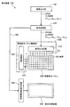
次に表示装置が備える機能の構成例について説明する。図25は表示装置が備える機能の構成例を示す図である。 Next, a configuration example of functions provided in the display device will be described. FIG. 25 is a diagram illustrating a configuration example of functions provided in the display device.
表示装置100は、画像出力部110と、信号処理部120とを含み、画像表示パネル駆動部400に出力信号SRGBWを、面状光源装置駆動部500に光源制御信号SBLをそれぞれ入力する。
The display device 100 includes an
画像出力部110は、入力信号SRGB(例えば、表示階調ビット数は8ビット)を信号処理部120に出力する。入力信号SRGBには、第1原色に対する入力信号値x1(p,q)、第2原色に対する入力信号値x2(p,q)、第3原色に対する入力信号値x3(p,q)が含まれる。第2の実施の形態では、第1原色は赤色、第2原色は緑色、第3原色は青色であるとする。
The
信号処理部120は、画像表示パネル200を駆動する画像表示パネル駆動部400と、面状光源装置300を駆動する面状光源装置駆動部500とに信号を供給する。信号処理部120は、入力信号SRGBに応じて画像表示パネル200の画素の輝度を調整する指標(または、面状光源装置300の輝度を削減する指標)を決定し、当該指標に応じて面状光源装置300の画素ごとの輝度情報を算出して出力信号SRGBW(例えば、表示階調ビット数は、8ビット)に反映し、面状光源装置300の画像表示を制御する。出力信号SRGBWには、第1副画素の出力信号値X1(p,q)、第2副画素の出力信号値X2(p,q)、第3副画素の出力信号値X3(p,q)に加え、第4の色を表示する第4副画素の出力信号値X4(p,q)が含まれる。第4の色は白色であるとする。
The
このような信号処理部120の処理動作は、図24に示した、表示用ドライバIC100bまたはCPU100a1等によって実現される。
Such processing operation of the
表示用ドライバIC100bで実現する場合には、CPU100a1を介して入力信号SRGBが表示用ドライバIC100bに入力される。表示用ドライバIC100bは、出力信号SRGBWを生成し、画像表示パネル200を制御する。また、光源制御信号SBLを生成し、バス100fを介してLEDドライバIC100cに送る。
When the
CPU100a1によって実現する場合には、表示用ドライバIC100bには、CPU100a1から出力信号SRGBWが入力される。また、光源制御信号SBLもCPU100a1によって生成され、バス100fを介してLEDドライバIC100cに送られる。
When realized by the CPU 100a1, the output signal SRGBW is input from the CPU 100a1 to the
なお、上記の照明装置または表示装置の処理機能は、コンピュータによって実現することができる。その場合、照明装置または表示装置が有すべき機能の処理内容を記述したプログラムが提供される。そのプログラムをコンピュータで実行することにより、上記処理機能がコンピュータ上で実現される。処理内容を記述したプログラムは、コンピュータで読み取り可能な記録媒体に記録しておくことができる。 Note that the processing functions of the illumination device or the display device described above can be realized by a computer. In that case, a program describing the processing content of the function that the lighting device or the display device should have is provided. By executing the program on a computer, the above processing functions are realized on the computer. The program describing the processing contents can be recorded on a computer-readable recording medium.
コンピュータで読み取り可能な記録媒体としては、磁気記憶装置、光ディスク、光磁気記録媒体、半導体メモリなどがある。磁気記憶装置には、ハードディスクドライブ(HDD:Hard Disk Drive)、フレキシブルディスク(FD)、磁気テープなどがある。光ディスクには、DVD(Digital Versatile Disc)、DVD−RAM(Random Access Memory)、CD−ROM(Compact Disc Read Only Memory)、CD−R(Recordable)/RW(Rewritable)などがある。光磁気記録媒体には、MO(Magneto-Optical disk)などがある。 Examples of the computer-readable recording medium include a magnetic storage device, an optical disk, a magneto-optical recording medium, and a semiconductor memory. Examples of the magnetic storage device include a hard disk drive (HDD), a flexible disk (FD), and a magnetic tape. Examples of the optical disc include a DVD (Digital Versatile Disc), a DVD-RAM (Random Access Memory), a CD-ROM (Compact Disc Read Only Memory), and a CD-R (Recordable) / RW (Rewritable). Magneto-optical recording media include MO (Magneto-Optical disk).
プログラムを流通させる場合には、たとえば、そのプログラムが記録されたDVD、CD−ROMなどの可搬型記録媒体が販売される。また、プログラムをサーバコンピュータの記憶装置に格納しておき、ネットワークを介して、サーバコンピュータから他のコンピュータにそのプログラムを転送することもできる。 When distributing the program, for example, portable recording media such as a DVD and a CD-ROM in which the program is recorded are sold. It is also possible to store the program in a storage device of a server computer and transfer the program from the server computer to another computer via a network.
プログラムを実行するコンピュータは、たとえば、可搬型記録媒体に記録されたプログラムもしくはサーバコンピュータから転送されたプログラムを、自己の記憶装置に格納する。 The computer that executes the program stores, for example, the program recorded on the portable recording medium or the program transferred from the server computer in its own storage device.
そして、コンピュータは、自己の記憶装置からプログラムを読み取り、プログラムにしたがった処理を実行する。なお、コンピュータは、可搬型記録媒体から直接プログラムを読み取り、そのプログラムにしたがった処理を実行することもできる。また、コンピュータは、ネットワークを介して接続されたサーバコンピュータからプログラムが転送されるごとに、逐次、受け取ったプログラムにしたがった処理を実行することもできる。 Then, the computer reads the program from its own storage device and executes processing according to the program. The computer can also read the program directly from the portable recording medium and execute processing according to the program. In addition, each time a program is transferred from a server computer connected via a network, the computer can sequentially execute processing according to the received program.
また、上記の処理機能の少なくとも一部を、DSP(Digital Signal Processor)、ASIC(Application Specific Integrated Circuit)、PLD(Programmable Logic Device)などの電子回路で実現することもできる。 In addition, at least a part of the above processing functions can be realized by an electronic circuit such as a DSP (Digital Signal Processor), an ASIC (Application Specific Integrated Circuit), or a PLD (Programmable Logic Device).
本発明の思想の範疇において、当業者であれば、各種の変更例及び修正例に想到し得るものであり、それら変更例及び修正例についても本発明の範囲に属するものと了解される。例えば、前述の各実施形態に対して、当業者が適宜、構成要素の追加、削除若しくは設計変更を行ったもの、または、工程の追加、省略もしくは条件変更を行ったものも、本発明の要旨を備えている限り、本発明の範囲に含まれる。 In the scope of the idea of the present invention, those skilled in the art can conceive various changes and modifications, and it is understood that these changes and modifications also belong to the scope of the present invention. For example, those in which the person skilled in the art has appropriately added, deleted, or changed the design of the above-described embodiments, or those in which processes have been added, omitted, or changed conditions are also the gist of the present invention. As long as it is provided, it is included in the scope of the present invention.
(1)開示される発明の一態様は、
光源と、
前記光源の輝度を制御するための、第1のビット数の第1の輝度制御信号に対して、前記第1の輝度制御信号で表現される値を、前記第1のビット数よりも小さな第2のビット数を持つ第2の輝度制御信号で時分割し、前記第2の輝度制御信号で表現される値に対応するパルス幅を持つ第3の輝度制御信号を生成する時分割制御部と、
前記第3の輝度制御信号にもとづいて、前記光源を発光させるための駆動信号を生成して、前記光源へ供給する駆動部と、
を有する照明装置である。
(1) One aspect of the disclosed invention is
A light source;
For a first luminance control signal having a first number of bits for controlling the luminance of the light source, a value expressed by the first luminance control signal is a value smaller than the first number of bits. A time division control unit for time-division using a second luminance control signal having a bit number of 2 and generating a third luminance control signal having a pulse width corresponding to a value represented by the second luminance control signal; ,
A drive unit that generates a drive signal for causing the light source to emit light based on the third luminance control signal, and supplies the drive signal to the light source;
It is an illuminating device which has.
(2)開示される発明の一態様は、
前記時分割制御部は、
前記第1のビット数をKビット、前記第2のビット数をL(<K)ビットとした場合、
前記第1の輝度制御信号の所定の時間領域から2K-L個の分割領域を生成し、
前記第1のビット数で表現される輝度階調の値を2K-Lで除算し、
前記分割領域に割り振られた値の総和を2K-Lで割った平均値が、前記除算の結果の値となるように、前記分割領域に対して、前記第2のビット数で表せる整数値を割り当てる、
(1)に記載の照明装置である。
(2) One aspect of the disclosed invention is as follows:
The time division control unit
When the first bit number is K bits and the second bit number is L (<K) bits,
Dividing the luminance gradation value expressed by the first number of bits by 2 KL ;
An integer value that can be expressed by the second number of bits is assigned to the divided area so that an average value obtained by dividing the sum of the values assigned to the divided area by 2 KL becomes a value resulting from the division. ,
It is an illuminating device as described in (1).
(3)開示される発明の一態様は、
前記時分割制御部は、前記除算の結果の整数部分と端数部分とに対して、前記端数部分に対応させた変化量を前記整数部分に加減算し、前記整数部分の値と、前記整数部分に加減算した値とで、前記分割領域に対して、前記第2のビット数で表せる整数値を割り当てる、
(2)に記載の照明装置である。
(3) One aspect of the disclosed invention is as follows:
The time division control unit adds or subtracts a change amount corresponding to the fractional part to the integer part and the integer part of the result of the division, and adds the value of the integer part to the integer part. An integer value that can be expressed by the second number of bits is assigned to the divided region with the added and subtracted values.
The lighting device according to (2).
(4)開示される発明の一態様は、
前記時分割制御部は、前記端数部分に対応させた変化量を前記整数部分に加減算して求めた値は、前記分割領域の中で分散させて割り当てる、
(3)に記載の照明装置である。
(4) One aspect of the disclosed invention is as follows:
The time division control unit assigns the value obtained by adding or subtracting the change amount corresponding to the fractional part to the integer part in a distributed manner in the divisional area.
It is an illuminating device as described in (3).
(5)開示される発明の一態様は、
前記第1のビット数の前記第1の輝度制御信号に対し、前記第1のビット数で表現される輝度階調の値を更新する更新部をさらに有し、前記更新部は、前記第3の輝度制御信号が第1の周期から第2の周期に切り替わるタイミングで、前記輝度階調の値を更新する、
(1)に記載の照明装置。
(5) One aspect of the disclosed invention is
The update unit further updates the luminance gradation value expressed by the first bit number with respect to the first luminance control signal having the first bit number, and the update unit includes the third luminance control signal. Updating the value of the luminance gradation at the timing when the luminance control signal is switched from the first period to the second period,
The lighting device according to (1).
(6)開示される発明の一態様は、
光源の輝度を制御するための、第1のビット数の第1の輝度制御信号に対して、前記第1の輝度制御信号で表現される値を、前記第1のビット数よりも小さな第2のビット数を持つ第2の輝度制御信号で時分割し、
前記第2の輝度制御信号で表現される値に対応するパルス幅を持つ第3の輝度制御信号を生成し、
前記第3の輝度制御信号にもとづいて、前記光源を発光させるための駆動信号を生成して、前記光源へ供給する照明制御方法である。
(6) One aspect of the disclosed invention is
For a first luminance control signal having a first number of bits for controlling the luminance of the light source, a value expressed by the first luminance control signal is set to a second value smaller than the first number of bits. Time-division with a second luminance control signal having the number of bits,
Generating a third luminance control signal having a pulse width corresponding to a value represented by the second luminance control signal;
The illumination control method generates a drive signal for causing the light source to emit light based on the third luminance control signal and supplies the drive signal to the light source.
(7)開示される発明の一態様は、
第1の副画素、第2の副画素および第3の副画素に対する第1の画像から伸長係数を算出し、光源の輝度を制御するための第1のビット数の第1の輝度制御信号を生成する画像解析部と、
前記伸長係数にもとづき、前記第1の副画素、前記第2の副画素、前記第3の副画素および前記第4の副画素に対する第2の画像を生成する画像生成部と、
前記第1の輝度制御信号で表現される値を、前記第1のビット数よりも小さな第2のビット数を持つ第2の輝度制御信号で時分割し、前記第2の輝度制御信号で表現される値に対応するパルス幅を持つ第3の輝度制御信号を生成し、前記第3の輝度制御信号にもとづいて、前記光源を制御するための駆動信号を生成し、前記光源へ供給する光源制御部と、
を有する表示装置である。
(7) One aspect of the disclosed invention is as follows:
The expansion coefficient is calculated from the first image for the first subpixel, the second subpixel, and the third subpixel, and the first luminance control signal having the first number of bits for controlling the luminance of the light source is obtained. An image analysis unit to be generated;
An image generation unit configured to generate a second image for the first subpixel, the second subpixel, the third subpixel, and the fourth subpixel based on the expansion coefficient;
A value expressed by the first luminance control signal is time-divided by a second luminance control signal having a second bit number smaller than the first bit number, and expressed by the second luminance control signal. A light source that generates a third luminance control signal having a pulse width corresponding to the value to be generated, generates a drive signal for controlling the light source based on the third luminance control signal, and supplies the drive signal to the light source A control unit;
It is a display apparatus which has.
(8)開示される発明の一態様は、
前記光源制御部は、
前記第1のビット数をKビット、前記第2のビット数をL(<K)ビットとした場合、
前記第1の輝度制御信号の所定の時間領域から2K-L個の分割領域を生成し、
前記第1のビット数で表現される輝度階調の値を2K-Lで除算し、
前記分割領域に割り振られた値の総和を2K-Lで割った平均値が、前記除算の結果の値となるように、前記分割領域に対して、前記第2のビット数で表せる整数値を割り当てる、
(7)に記載の表示装置である。
(8) One aspect of the disclosed invention is
The light source controller is
When the first bit number is K bits and the second bit number is L (<K) bits,
Dividing the luminance gradation value expressed by the first number of bits by 2 KL ;
An integer value that can be expressed by the second number of bits is assigned to the divided area so that an average value obtained by dividing the sum of the values assigned to the divided area by 2 KL becomes a value resulting from the division. ,
(7) It is a display apparatus as described in.
(9)開示される発明の一態様は、
前記光源制御部は、前記除算の結果の整数部分と端数部分とに対して、前記端数部分に対応させた変化量を前記整数部分に加減算し、前記整数部分の値と、前記整数部分に加減算した値とで、前記分割領域に対して、前記第2のビット数で表せる整数値を割り当てる、
(8)に記載の表示装置である。
(9) One aspect of the disclosed invention is
The light source control unit adds or subtracts a change amount corresponding to the fractional part with respect to the integer part and fractional part of the division result, and adds or subtracts the value of the integer part and the integer part. And assigning an integer value that can be expressed by the second number of bits to the divided region.
The display device according to (8).
1……照明装置、1a……時分割制御部、1b……駆動部、1c……光源、P1、P2、P3……輝度制御信号、dr……駆動信号、w1、w2……パルス幅
DESCRIPTION OF
Claims (9)
前記光源の輝度を制御するための、第1のビット数の第1の輝度制御信号に対して、前記第1の輝度制御信号で表現される値を、前記第1のビット数よりも小さな第2のビット数を持つ第2の輝度制御信号で時分割し、前記第2の輝度制御信号で表現される値に対応するパルス幅を持つ第3の輝度制御信号を生成する時分割制御部と、
前記第3の輝度制御信号にもとづいて、前記光源を発光させるための駆動信号を生成して、前記光源へ供給する駆動部と、
を有する照明装置。 A light source;
For a first luminance control signal having a first number of bits for controlling the luminance of the light source, a value expressed by the first luminance control signal is a value smaller than the first number of bits. A time division control unit for time-division using a second luminance control signal having a bit number of 2 and generating a third luminance control signal having a pulse width corresponding to a value represented by the second luminance control signal; ,
A drive unit that generates a drive signal for causing the light source to emit light based on the third luminance control signal, and supplies the drive signal to the light source;
A lighting device.
前記第1のビット数をKビット、前記第2のビット数をL(<K)ビットとした場合、
前記第1の輝度制御信号の所定の時間領域から2K-L個の分割領域を生成し、
前記第1のビット数で表現される輝度階調の値を2K-Lで除算し、
前記分割領域に割り振られた値の総和を2K-Lで割った平均値が、前記除算の結果の値となるように、前記分割領域に対して、前記第2のビット数で表せる整数値を割り当てる、
請求項1に記載の照明装置。 The time division control unit
When the first bit number is K bits and the second bit number is L (<K) bits,
Generating 2 KL divided regions from a predetermined time region of the first luminance control signal;
Dividing the luminance gradation value expressed by the first number of bits by 2 KL ;
An integer value that can be expressed by the second number of bits is assigned to the divided area so that an average value obtained by dividing the sum of the values assigned to the divided area by 2 KL becomes a value resulting from the division. ,
The lighting device according to claim 1.
請求項2に記載の照明装置。 The time division control unit adds or subtracts a change amount corresponding to the fractional part to the integer part and the integer part of the result of the division, and adds the value of the integer part to the integer part. An integer value that can be expressed by the second number of bits is assigned to the divided region with the added and subtracted values.
The lighting device according to claim 2.
請求項3に記載の照明装置。 The time division control unit assigns the value obtained by adding or subtracting the change amount corresponding to the fractional part to the integer part in a distributed manner in the divisional area.
The lighting device according to claim 3.
請求項1に記載の照明装置。 The update unit further updates the luminance gradation value expressed by the first bit number with respect to the first luminance control signal having the first bit number, and the update unit includes the third luminance control signal. Updating the value of the luminance gradation at the timing when the luminance control signal is switched from the first period to the second period,
The lighting device according to claim 1.
前記第2の輝度制御信号で表現される値に対応するパルス幅を持つ第3の輝度制御信号を生成し、
前記第3の輝度制御信号にもとづいて、前記光源を発光させるための駆動信号を生成して、前記光源へ供給する照明制御方法。 For a first luminance control signal having a first number of bits for controlling the luminance of the light source, a value expressed by the first luminance control signal is set to a second value smaller than the first number of bits. Time-division with a second luminance control signal having the number of bits,
Generating a third luminance control signal having a pulse width corresponding to a value represented by the second luminance control signal;
An illumination control method for generating a drive signal for causing the light source to emit light based on the third luminance control signal and supplying the drive signal to the light source.
前記伸長係数にもとづき、前記第1の副画素、前記第2の副画素、前記第3の副画素および前記第4の副画素に対する第2の画像を生成する画像生成部と、
前記第1の輝度制御信号で表現される値を、前記第1のビット数よりも小さな第2のビット数を持つ第2の輝度制御信号で時分割し、前記第2の輝度制御信号で表現される値に対応するパルス幅を持つ第3の輝度制御信号を生成し、前記第3の輝度制御信号にもとづいて、前記光源を制御するための駆動信号を生成し、前記光源へ供給する光源制御部と、
を有する表示装置。 The expansion coefficient is calculated from the first image for the first subpixel, the second subpixel, and the third subpixel, and the first luminance control signal having the first number of bits for controlling the luminance of the light source is obtained. An image analysis unit to be generated;
An image generation unit configured to generate a second image for the first subpixel, the second subpixel, the third subpixel, and the fourth subpixel based on the expansion coefficient;
A value expressed by the first luminance control signal is time-divided by a second luminance control signal having a second bit number smaller than the first bit number, and expressed by the second luminance control signal. A light source that generates a third luminance control signal having a pulse width corresponding to the value to be generated, generates a drive signal for controlling the light source based on the third luminance control signal, and supplies the drive signal to the light source A control unit;
A display device.
前記第1のビット数をKビット、前記第2のビット数をL(<K)ビットとした場合、
前記第1の輝度制御信号の所定の時間領域から2K-L個の分割領域を生成し、
前記第1のビット数で表現される輝度階調の値を2K-Lで除算し、
前記分割領域に割り振られた値の総和を2K-Lで割った平均値が、前記除算の結果の値となるように、前記分割領域に対して、前記第2のビット数で表せる整数値を割り当てる、
請求項7に記載の表示装置。 The light source controller is
When the first bit number is K bits and the second bit number is L (<K) bits,
Generating 2 KL divided regions from a predetermined time region of the first luminance control signal;
Dividing the luminance gradation value expressed by the first number of bits by 2 KL ;
An integer value that can be expressed by the second number of bits is assigned to the divided area so that an average value obtained by dividing the sum of the values assigned to the divided area by 2 KL becomes a value resulting from the division. ,
The display device according to claim 7.
請求項8に記載の表示装置。 The light source control unit adds or subtracts a change amount corresponding to the fractional part with respect to the integer part and fractional part of the division result, and adds or subtracts the value of the integer part and the integer part. And assigning an integer value that can be expressed by the second number of bits to the divided region.
The display device according to claim 8.
Priority Applications (2)
| Application Number | Priority Date | Filing Date | Title |
|---|---|---|---|
| JP2014090316A JP2015210323A (en) | 2014-04-24 | 2014-04-24 | Lighting unit, lighting control method, and display device |
| US14/682,520 US9972253B2 (en) | 2014-04-24 | 2015-04-09 | Illumination apparatus, illumination control method, and display apparatus |
Applications Claiming Priority (1)
| Application Number | Priority Date | Filing Date | Title |
|---|---|---|---|
| JP2014090316A JP2015210323A (en) | 2014-04-24 | 2014-04-24 | Lighting unit, lighting control method, and display device |
Publications (1)
| Publication Number | Publication Date |
|---|---|
| JP2015210323A true JP2015210323A (en) | 2015-11-24 |
Family
ID=54335340
Family Applications (1)
| Application Number | Title | Priority Date | Filing Date |
|---|---|---|---|
| JP2014090316A Pending JP2015210323A (en) | 2014-04-24 | 2014-04-24 | Lighting unit, lighting control method, and display device |
Country Status (2)
| Country | Link |
|---|---|
| US (1) | US9972253B2 (en) |
| JP (1) | JP2015210323A (en) |
Families Citing this family (1)
| Publication number | Priority date | Publication date | Assignee | Title |
|---|---|---|---|---|
| US11694641B2 (en) * | 2021-09-24 | 2023-07-04 | Apple Inc. | Systems and methods for increasing a pulse width modulation frequency while preserving resolution |
Family Cites Families (5)
| Publication number | Priority date | Publication date | Assignee | Title |
|---|---|---|---|---|
| JP2007322881A (en) | 2006-06-02 | 2007-12-13 | Sony Corp | Display device and display control method |
| JP2010002876A (en) | 2008-05-19 | 2010-01-07 | Sony Ericsson Mobilecommunications Japan Inc | Display device, display control method, and display control program |
| JP5386211B2 (en) | 2008-06-23 | 2014-01-15 | 株式会社ジャパンディスプレイ | Image display device and driving method thereof, and image display device assembly and driving method thereof |
| JP5568074B2 (en) | 2008-06-23 | 2014-08-06 | 株式会社ジャパンディスプレイ | Image display device and driving method thereof, and image display device assembly and driving method thereof |
| KR20110017777A (en) * | 2009-08-14 | 2011-02-22 | 삼성에스디아이 주식회사 | Light emitting device and driving method the same |
-
2014
- 2014-04-24 JP JP2014090316A patent/JP2015210323A/en active Pending
-
2015
- 2015-04-09 US US14/682,520 patent/US9972253B2/en active Active
Also Published As
| Publication number | Publication date |
|---|---|
| US9972253B2 (en) | 2018-05-15 |
| US20150310828A1 (en) | 2015-10-29 |
Similar Documents
| Publication | Publication Date | Title |
|---|---|---|
| CN111489685B (en) | Multi-line scanning LED gray scale switching display method and system | |
| JP7109436B2 (en) | Intensity Scaled Dithering Pulse Width Modulation | |
| TWI506609B (en) | Method for adjusting gamma curve and gamma voltage generator and display control system therof | |
| CN109754741B (en) | Apparatus and method for display brightness control | |
| TW201824237A (en) | Organic light emitting display device, data driver, method for driving data driver, display device, and method for driving display device | |
| TW201346874A (en) | Display device | |
| JP4707381B2 (en) | Electron emission display device having variable gradation expression power | |
| WO2016084544A1 (en) | Pixel unit, display panel, and signal transmission method | |
| JP6659178B2 (en) | Image processing apparatus and image processing method | |
| CN111583845A (en) | Source driver and display device comprising same | |
| JPWO2011158541A1 (en) | Display signal generator, display device, and image display method | |
| JP2017015751A (en) | Display panel driver, display unit, and driving method for display panel | |
| JP2016048334A (en) | Illumination device, illumination control method, and display device | |
| US10297212B2 (en) | Display device and display device drive method | |
| TW201942893A (en) | Digital driving of active matrix displays capable of increasing PWM depth | |
| JP2015210323A (en) | Lighting unit, lighting control method, and display device | |
| JP2019028291A (en) | Display driver, display controller, electro-optic device, and electronic apparatus | |
| TW201528869A (en) | Binary distribution control method of multi-channel light emitting diode driving system | |
| WO2019058787A1 (en) | Display device and drive method for display device | |
| US8767000B2 (en) | Data processing method and display apparatus for performing the same | |
| JP5906631B2 (en) | Display device, display method, and electronic apparatus | |
| TW202247641A (en) | Method and apparatus of generating drive signal for light emitting element | |
| JP2018194567A (en) | Light-emitting device, display device and method for controlling light-emitting device | |
| WO2017187837A1 (en) | Image display device and image display method | |
| KR101142934B1 (en) | Driver and display having the same |