JP2015201567A - plasma processing apparatus and method - Google Patents
plasma processing apparatus and method Download PDFInfo
- Publication number
- JP2015201567A JP2015201567A JP2014080213A JP2014080213A JP2015201567A JP 2015201567 A JP2015201567 A JP 2015201567A JP 2014080213 A JP2014080213 A JP 2014080213A JP 2014080213 A JP2014080213 A JP 2014080213A JP 2015201567 A JP2015201567 A JP 2015201567A
- Authority
- JP
- Japan
- Prior art keywords
- gas
- plasma processing
- mounting table
- axis
- processing apparatus
- Prior art date
- Legal status (The legal status is an assumption and is not a legal conclusion. Google has not performed a legal analysis and makes no representation as to the accuracy of the status listed.)
- Withdrawn
Links
Images


Classifications
-
- H—ELECTRICITY
- H01—ELECTRIC ELEMENTS
- H01J—ELECTRIC DISCHARGE TUBES OR DISCHARGE LAMPS
- H01J37/00—Discharge tubes with provision for introducing objects or material to be exposed to the discharge, e.g. for the purpose of examination or processing thereof
- H01J37/32—Gas-filled discharge tubes
- H01J37/32431—Constructional details of the reactor
- H01J37/3244—Gas supply means
-
- H—ELECTRICITY
- H01—ELECTRIC ELEMENTS
- H01J—ELECTRIC DISCHARGE TUBES OR DISCHARGE LAMPS
- H01J37/00—Discharge tubes with provision for introducing objects or material to be exposed to the discharge, e.g. for the purpose of examination or processing thereof
- H01J37/32—Gas-filled discharge tubes
- H01J37/32009—Arrangements for generation of plasma specially adapted for examination or treatment of objects, e.g. plasma sources
- H01J37/32192—Microwave generated discharge
- H01J37/32211—Means for coupling power to the plasma
- H01J37/3222—Antennas
Landscapes
- Physics & Mathematics (AREA)
- Engineering & Computer Science (AREA)
- Plasma & Fusion (AREA)
- Chemical & Material Sciences (AREA)
- Analytical Chemistry (AREA)
- Drying Of Semiconductors (AREA)
- Plasma Technology (AREA)
- General Physics & Mathematics (AREA)
- Condensed Matter Physics & Semiconductors (AREA)
- Manufacturing & Machinery (AREA)
- Computer Hardware Design (AREA)
- Microelectronics & Electronic Packaging (AREA)
- Power Engineering (AREA)
- Spectroscopy & Molecular Physics (AREA)
- Electromagnetism (AREA)
- Chemical Vapour Deposition (AREA)
Abstract
Description
本発明の実施形態は、プラズマ処理装置及びプラズマ処理方法に関するものである。 Embodiments described herein relate generally to a plasma processing apparatus and a plasma processing method.
電子デバイスの製造においては、被処理体に対してプラズマエッチングといったプラズマ処理が施される。このようなプラズマ処理では、被処理体に対する処理に面内均一性が要求される。 In manufacturing an electronic device, a plasma process such as plasma etching is performed on an object to be processed. In such plasma processing, in-plane uniformity is required for processing on an object to be processed.
下記の特許文献1には、このような要求に対して提案された一種のプラズマ処理装置が記載されている。特許文献1に記載されたプラズマ処理装置は、マイクロ波によってプラズマを発生させるプラズマ処理装置であり、載置台、中央導入部、及び周辺導入部を有している。載置台は、その上に被処理体を載置する。中央導入部は、載置台の中心を鉛直方向に通る軸線に沿って載置台の上方からガスを導入する。また、周辺導入部は、中央導入部のガス吐出口と載置台との間の高さ位置において環状に延在する管からガスを導入する。この周辺導入部の管には、周方向に配列された複数のガス吐出口が形成されている。これら複数のガス吐出口は、載置台の上面と略平行に上記軸線に向けて延びている。即ち、周辺導入部のガス吐出口は、軸線に対して垂直に当該軸線に向けて延びている。 The following Patent Document 1 describes a kind of plasma processing apparatus proposed for such a requirement. The plasma processing apparatus described in Patent Document 1 is a plasma processing apparatus that generates plasma by microwaves, and includes a mounting table, a central introduction unit, and a peripheral introduction unit. A mounting table mounts a to-be-processed object on it. The central introduction part introduces gas from above the mounting table along an axis passing through the center of the mounting table in the vertical direction. Further, the peripheral introduction part introduces gas from a pipe extending in an annular shape at a height position between the gas discharge port of the central introduction part and the mounting table. A plurality of gas discharge ports arranged in the circumferential direction are formed in the pipe of the peripheral introduction portion. The plurality of gas discharge ports extend toward the axis substantially parallel to the upper surface of the mounting table. That is, the gas discharge port of the peripheral introduction portion extends toward the axis perpendicular to the axis.
特許文献1に記載されたプラズマ処理装置では、周辺導入部からガスが上記軸線に向けて吐出された後、当該ガスの流れは、上方に向かう流れと、下方、即ち載置台に向かう流れとに分離される。したがって、周辺導入部から導入されて被処理体に向かうガスの流れと中央導入部から導入されるガスとは、被処理体上において衝突し得る。これにより、被処理体上にはガスが滞留する領域が生じ得る。かかる領域が生じると、被処理体に対する処理が不均一となる。 In the plasma processing apparatus described in Patent Document 1, after the gas is discharged from the peripheral introduction portion toward the axis, the flow of the gas is divided into an upward flow and a downward flow, that is, a flow toward the mounting table. To be separated. Therefore, the gas flow introduced from the peripheral introduction part toward the object to be processed and the gas introduced from the central introduction part can collide on the object to be processed. Thereby, the area | region where gas stagnates on a to-be-processed object may arise. When such a region is generated, processing on the object to be processed becomes non-uniform.
したがって、プラズマ処理装置には、被処理体上でのガスの滞留を抑制することが必要となっている。 Therefore, it is necessary for the plasma processing apparatus to suppress gas stagnation on the object to be processed.
一側面においては被処理体に対してプラズマ処理を行うためのプラズマ処理装置が提供される。このプラズマ処理装置は、処理容器、載置台、中央導入部、及び、周辺導入部を有している。処理容器は、後述する軸線に沿って延びる側壁を有している。載置台は、処理容器内に設けられている。中央導入部は、載置台の上方に設けられており、載置台の中心を通る軸線に沿って当該載置台に向けてガスを導入する。周辺導入部は、軸線が延在する方向、即ち高さ方向においては、中央導入部と載置台の上面との間に設けられている。また、周辺導入部は、側壁に沿って設けられている。即ち、周辺導入部は、側壁に接するように設けられている。周辺導入部は、前記軸線に対して周方向に配列された複数のガス吐出口を提供している。周辺導入部の複数のガス吐出口は、前記軸線に近づくにつれて前記載置台から離れるように延びている。換言すると、これら複数のガス吐出口は、処理容器内の空間の中央に向かう成分と前記軸線に沿って載置台から離れる成分とをもつ方向、即ち、斜め上方に延びている。 In one aspect, a plasma processing apparatus for performing plasma processing on an object to be processed is provided. This plasma processing apparatus has a processing container, a mounting table, a central introduction part, and a peripheral introduction part. The processing container has a side wall extending along an axis described later. The mounting table is provided in the processing container. The central introduction part is provided above the mounting table, and introduces gas toward the mounting table along an axis passing through the center of the mounting table. The peripheral introduction portion is provided between the central introduction portion and the upper surface of the mounting table in the direction in which the axis extends, that is, in the height direction. Moreover, the periphery introduction part is provided along the side wall. That is, the peripheral introduction part is provided in contact with the side wall. The peripheral introduction portion provides a plurality of gas discharge ports arranged in the circumferential direction with respect to the axis. The plurality of gas discharge ports of the peripheral introduction portion extend away from the mounting table as approaching the axis. In other words, the plurality of gas discharge ports extend in a direction having a component toward the center of the space in the processing container and a component away from the mounting table along the axis, that is, obliquely upward.
このプラズマ処理装置によれば、周辺導入部から導入されたガスは、斜め上方に向かって流れ、中央導入部から導入されるガスと合流し、或いは、中央導入部から導入されるガスの流れに沿って流れる。したがって、載置台上に載置された被処理体上では、ガスは被処理体の中心から被処理体のエッジに向かう方向に流れるようになる。故に、被処理体上でのガスの滞留が抑制される。 According to this plasma processing apparatus, the gas introduced from the peripheral introduction portion flows obliquely upward, merges with the gas introduced from the central introduction portion, or flows into the gas flow introduced from the central introduction portion. Flowing along. Therefore, on the object to be processed placed on the mounting table, the gas flows from the center of the object to be processed toward the edge of the object to be processed. Therefore, stagnation of gas on the object to be processed is suppressed.
一形態においては、周辺導入部の複数のガス吐出口は、前記軸線に垂直な面に対して15度以上60度以下の角度を有するように延在していてもよい。 In one embodiment, the plurality of gas discharge ports of the peripheral introduction portion may extend so as to have an angle of 15 degrees or more and 60 degrees or less with respect to a plane perpendicular to the axis.
一形態においてプラズマ処理装置は、処理容器内にマイクロ波を導入するためのアンテナを更に有し得る。このアンテナは、載置台の上方において載置台と対面するように設けられており、且つ、処理容器内の空間に接する誘電体窓を有する。誘電体窓には前記軸線に沿って延びる中央導入部のガス吐出口が形成されている。一形態において、アンテナは、ラジアルラインスロットアンテナであり得る。 In one form, the plasma processing apparatus may further include an antenna for introducing a microwave into the processing container. This antenna is provided above the mounting table so as to face the mounting table, and has a dielectric window in contact with the space in the processing container. The dielectric window is formed with a gas outlet of the central introduction portion extending along the axis. In one form, the antenna may be a radial line slot antenna.
別の一側面においては、上述した一側面及び種々の形態のうち何れかのプラズマ処理装置を用いたプラズマ処理方法が提供される。このプラズマ処理方法では、中央導入部及び周辺導入部からガスが導入され、該ガスのプラズマにより載置台上に載置された被処理体が処理される。このプラズマ処理方法によれば、被処理体の処理の面内均一性が向上され得る。 In another aspect, there is provided a plasma processing method using the plasma processing apparatus according to any one of the above aspects and various forms. In this plasma processing method, gas is introduced from the central introduction portion and the peripheral introduction portion, and the object to be processed placed on the placement table is processed by the plasma of the gas. According to this plasma processing method, the in-plane uniformity of processing of the object to be processed can be improved.
一形態において、被処理体は、シリコン、ゲルマニウム、又はシリコンゲルマニウムから構成された膜を有し、前記ガスは、当該膜に対して腐食性を有するガスを含み得る。このようなガスの例は、HBrガスを含むガスであり得る。 In one embodiment, the object to be processed includes a film made of silicon, germanium, or silicon germanium, and the gas may include a gas that is corrosive to the film. An example of such a gas may be a gas containing HBr gas.
以上説明したように、被処理体上でのガスの滞留を抑制することが可能なプラズマ処理装置、及び当該プラズマ処理装置を用いたプラズマ処理方法が提供される。 As described above, a plasma processing apparatus capable of suppressing gas stagnation on an object to be processed and a plasma processing method using the plasma processing apparatus are provided.
以下、図面を参照して種々の実施形態について詳細に説明する。なお、各図面において同一又は相当の部分に対しては同一の符号を附すこととする。 Hereinafter, various embodiments will be described in detail with reference to the drawings. In the drawings, the same or corresponding parts are denoted by the same reference numerals.
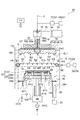
まず、一実施形態に係るプラズマ処理装置について説明する。図1は、一実施形態に係るプラズマ処理装置を概略的に示す断面図である。図1に示すプラズマ処理装置10は、処理容器12を備えている。処理容器12は、被処理体を収容するための処理空間Sを提供している。なお、以下の説明では、被処理体のことを、ウエハWということがある。
First, a plasma processing apparatus according to an embodiment will be described. FIG. 1 is a cross-sectional view schematically showing a plasma processing apparatus according to an embodiment. A
処理容器12は、側壁12aを含んでいる。また、処理容器12は、底部12b、及び、天部12cを更に含み得る。側壁12aは、軸線Zが延びる方向に延在する略円筒形状を有している。この軸線Zは、例えば、後述する載置台の中心を鉛直方向に通る軸線である。一実施形態では、側壁12aの中心軸線は、軸線Zと一致している。この側壁12aの内径は、例えば、540mmである。
The
底部12bは、側壁12aの下端側に設けられている。また、側壁12aの上端部は開口している。側壁12aの上端部開口は、誘電体窓18によって閉じられている。誘電体窓18は、側壁12aの上端部と天部12cとの間に挟持されている。この誘電体窓18と側壁12aの上端部との間には封止部材SL1が介在していてもよい。封止部材SL1は、例えばOリングであり、処理容器12の密閉に寄与する。
The bottom 12b is provided on the lower end side of the
プラズマ処理装置10は、処理容器12内に設けられた載置台20を更に備えている。載置台20は、誘電体窓18の下方に設けられている。例えば、誘電体窓18の下面と載置台20の上面との間の距離は、245mmである。一実施形態においては、載置台20は、下部電極LE、及び、静電チャックESCを含んでいる。
The
下部電極LEは、第1プレート22a及び第2プレート22bを含んでいる。第1プレート22a及び第2プレート22bは共に、略円盤形状を有しており、例えば、アルミニウムから構成されている。第1プレート22aは、筒状の支持部SP1によって支持されている。支持部SP1は、底部12bから垂直上方に延びている。第2プレート22bは、第1プレート22a上に設けられており、第1プレート22aに導通している。
The lower electrode LE includes a first plate 22a and a
下部電極LEは、給電棒PFR及びマッチングユニットMUを介して、高周波電源RFGに電気的に接続されている。高周波電源RFGは、高周波バイアス電力を下部電極LEに供給する。高周波電源RFGによって発生される高周波バイアス電力は、ウエハWに引き込むイオンのエネルギーを制御するのに適した一定の周波数、例えば、13.65MHzの周波数を有し得る。マッチングユニットMUは、高周波電源RFG側のインピーダンスと、主に電極、プラズマ、処理容器12といった負荷側のインピーダンスとの間で整合をとるための整合器を収容している。この整合器の中には、例えば、自己バイアス生成用のブロッキングコンデンサが含まれ得る。
The lower electrode LE is electrically connected to the high frequency power supply RFG via the power supply rod PFR and the matching unit MU. The high frequency power supply RFG supplies high frequency bias power to the lower electrode LE. The high frequency bias power generated by the high frequency power supply RFG may have a certain frequency suitable for controlling the energy of ions drawn into the wafer W, for example, a frequency of 13.65 MHz. The matching unit MU accommodates a matching unit for matching between the impedance on the high frequency power supply RFG side and the impedance on the load side such as an electrode, plasma, and the
静電チャックESCは、第2プレート22b上に設けられている。静電チャックESCは、処理空間S側にウエハWを載置するための載置領域MRを提供している。載置領域MRは、軸線Zに略直交する略円形の領域であり、ウエハWの直径と略同一の直径又はウエハWの直径よりも若干小さい直径を有し得る。また、この載置領域MRは、載置台20の上面を構成しており、当該載置領域MRの中心、即ち、載置台20の中心は、軸線Z上に位置している。
The electrostatic chuck ESC is provided on the
静電チャックESCは、ウエハWを静電吸着力により保持する。静電チャックESCは、誘電体内に設けられた吸着用電極を含んでいる。静電チャックESCの吸着用電極には、直流電源DCSがスイッチSW及び被覆線CLを介して接続されている。静電チャックESCは、直流電源DCSから印加される直流電圧により発生するクーロン力によって、その上面にウエハWを吸着して、当該ウエハWを保持することができる。この静電チャックESCの径方向外側には、ウエハWの周囲を環状に囲むフォーカスリングFRが設けられている。 The electrostatic chuck ESC holds the wafer W by electrostatic attraction force. The electrostatic chuck ESC includes an attracting electrode provided in a dielectric. A DC power source DCS is connected to the chucking electrode of the electrostatic chuck ESC via a switch SW and a covered wire CL. The electrostatic chuck ESC can hold the wafer W by adsorbing the wafer W on the upper surface by a Coulomb force generated by a DC voltage applied from the DC power source DCS. On the outer side in the radial direction of the electrostatic chuck ESC, a focus ring FR that surrounds the periphery of the wafer W in an annular shape is provided.
第2プレート22bの内部には、環状の流路24gが形成されている。この流路24gには、チラーユニットから配管PP1を介して冷媒が供給される。流路24gに供給された冷媒は、配管PP3を介してチラーユニットに回収される。さらに、プラズマ処理装置10では、伝熱ガス供給部からの伝熱ガス、例えば、Heガスが供給管PP2を介して静電チャックESCの上面とウエハWの裏面との間に供給される。
An
載置台20の外周の外側、即ち、載置台20と側壁12aとの間には、空間が提供されている。この空間は、平面視においては環形状を有する排気路VLとなっている。排気路VLの軸線Z方向における中間には、複数の貫通孔が形成された環状のバッフル板26が設けられている。排気路VLは、排気口28hを提供する排気管28に接続している。排気管28は、処理容器12の底部12bに取り付けられている。この排気管28には、排気装置30が接続されている。排気装置30は、圧力調整器、及びターボ分子ポンプなどの真空ポンプを有している。この排気装置30により、処理容器12内の処理空間Sを所望の真空度まで減圧することができる。また、ウエハWに対して供給されたガスは、排気装置30を動作させることにより、ウエハWの表面に沿って当該ウエハWのエッジの外側に向けて流れ、載置台20の外周から排気路VLを介して排気されるようになっている。
A space is provided outside the outer periphery of the mounting table 20, that is, between the mounting table 20 and the
一実施形態においては、プラズマ処理装置10は、温度制御機構として、ヒータHT、HS、HC、及び、HEを更に備え得る。ヒータHTは、天部12c内に設けられており、アンテナ14を囲むように、環状に延在している。また、ヒータHSは、側壁12a内に設けられており、環状に延在している。ヒータHCは、第2プレート22b内又は静電チャックESC内に設けられている。ヒータHCは、上述した載置領域MRの中央部分の下方、即ち軸線Zに交差する領域に設けられている。また、ヒータHEは、ヒータHCを囲むように環状に延在している。ヒータHEは、上述した載置領域MRの外縁部分の下方に設けられている。
In one embodiment, the
一実施形態においては、プラズマ処理装置10は、アンテナ14、同軸導波管16、マイクロ波発生器32、チューナ34、導波管36、及び、モード変換器38を更に備え得る。これらアンテナ14、同軸導波管16、誘電体窓18、マイクロ波発生器32、チューナ34、導波管36、及び、モード変換器38は、処理容器内に導入されるガスを励起させるためのプラズマ生成源を構成している。
In one embodiment, the
マイクロ波発生器32は、例えば2.45GHzの周波数のマイクロ波を発生する。マイクロ波発生器32は、チューナ34、導波管36、及びモード変換器38を介して、同軸導波管16の上部に接続されている。同軸導波管16は、その中心軸線である軸線Zに沿って延在している。
The
同軸導波管16は、外側導体16a及び内側導体16bを含んでいる。外側導体16aは、軸線Z中心に延在する円筒形状を有している。外側導体16aの下端は、導電性の表面を有する冷却ジャケット40の上部に電気的に接続されている。内側導体16bは、外側導体16aの内側において、当該外側導体16aと同軸に設けられている。内側導体16bは、軸線Z中心に延在する円筒形状を有している。内側導体16bの下端は、アンテナ14のスロット板44に接続している。
The
一実施形態においては、アンテナ14は、ラジアルラインスロットアンテナである。このアンテナ14は、載置台20と対面するよう、天部12cに形成された開口内に配置されている。アンテナ14は、誘電体板42、スロット板44、及び誘電体窓18を含んでいる。誘電体板42は、マイクロ波の波長を短縮させるものであり、略円盤形状を有している。誘電体板42は、例えば、石英又はアルミナから構成される。この誘電体板42は、スロット板44と冷却ジャケット40の下面の間に挟持されている。
In one embodiment, the
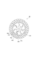
図2は、スロット板の一例を示す平面図である。スロット板44は、薄板状であって、円板状である。スロット板44の板厚方向の両面は、それぞれ平らである。スロット板44の中心CSは、軸線Z上に位置している。スロット板44には、複数のスロット対44pが設けられている。複数のスロット対44pの各々は、板厚方向に貫通する二つのスロット孔44a,44bを含んでいる。スロット孔44a,44bそれぞれの平面形状は、長孔形状である。各スロット対44pにおいて、スロット孔44aの長軸が延びる方向と、スロット孔44bの長軸が延びる方向は、互いに交差又は直交している。これら複数のスロット対44pは、周方向に配列されている。図2に示す例では、二つの同心円に沿って、複数のスロット対44pが周方向に配列されている。各同心円上では、スロット対44pは、略等間隔で配列されている。このスロット板44は、誘電体窓18上の上面18uに設けられている。
FIG. 2 is a plan view showing an example of the slot plate. The
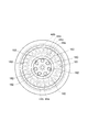
図3は、誘電体窓の一例を示す平面図であり、図4は、図3のIV−IV線に沿ってとった断面図である。図3及び図4に示すように、誘電体窓18は、石英といった誘電体製の略円盤状の部材である。誘電体窓18の中央には、貫通孔18hが形成されている。貫通孔18hの上側部分は、後述する中央導入部50のインジェクタ50bが収容される空間18sであり、下側部分は、後述する中央導入部50のガス吐出口18iである。なお、誘電体窓18の中心軸線は、軸線Zと一致している。
FIG. 3 is a plan view showing an example of a dielectric window, and FIG. 4 is a cross-sectional view taken along line IV-IV in FIG. As shown in FIGS. 3 and 4, the
誘電体窓の上面18uと反対側の面、即ち下面18bは、処理空間Sに接しており、プラズマを生成する側の面である。この下面18bは、種々の形状を画成している。具体的に、下面18bは、ガス吐出口18iを囲む中央領域において、平坦面180を有している。この平坦面180は、軸線Zに直交する平坦な面である。下面18bは、環状の第1凹部181を画成している。第1凹部181は、平坦面180の径方向外側領域において、環状に連なり誘電体窓18の板厚方向内方側に向かってテーパ状に窪んでいる。
The surface opposite to the
また、下面18bは、複数の第2凹部182を画成している。これら複数の第2凹部182は、平坦面180から板厚方向内方側に向かって窪んでいる。複数の第2凹部182の個数は、図3及び図4に示す例では、7個である。これら複数の第2凹部182は、周方向に沿って等間隔に形成されている。また、複数の第2凹部182は、軸線Zに直交する面において円形の平面形状を有している。
The
図5は、図3に示す誘電体窓上に図2に示すスロット板を設けた状態を示す平面図であり、誘電体窓18を下側から見た状態を示している。図5に示すように、平面視において、即ち、軸線Z方向に見ると、径方向外側の同心円に沿って設けられたスロット対44pは、第1凹部181に重なっている。また、径方向内側の同心円に沿って設けられたスロット対44pのスロット孔44bは、第1凹部181に重なっている。さらに、径方向内側の同心円に沿って設けられたスロット対44pのスロット孔44aは、複数の第2凹部182に重なっている。
FIG. 5 is a plan view showing a state in which the slot plate shown in FIG. 2 is provided on the dielectric window shown in FIG. 3, and shows a state where the
図1を再び参照する。プラズマ処理装置10では、マイクロ波発生器32により発生されたマイクロ波が、同軸導波管16を通って、誘電体板42に伝播され、スロット板44のスロット孔44a及び44bから誘電体窓18に与えられる。誘電体窓18の直下においては、比較的薄い板厚を有する部分によって画成された第1凹部181及び第2凹部182にマイクロ波のエネルギーが集中する。したがって、このプラズマ処理装置10では、周方向及び径方向に安定して分布するようにプラズマを発生させることが可能となる。
Please refer to FIG. 1 again. In the
また、プラズマ処理装置10は、中央導入部50及び周辺導入部52を備えている。中央導入部50は、導管50a、インジェクタ50b、及びガス吐出口18iを含んでいる。導管50aは、同軸導波管16の内側導体16bの内孔に通されている。また、導管50aの端部は、誘電体窓18が軸線Zに沿って画成する空間18s(図4参照)内まで延在している。この空間18s内且つ導管50aの端部の下方には、インジェクタ50bが収容されている。インジェクタ50bには、軸線Z方向に延びる複数の貫通孔が設けられている。また、誘電体窓18は、上述したガス吐出口18iを提供している。ガス吐出口18iは、空間18sの下方に連続し、且つ軸線Zに沿って延びている。かかる構成の中央導入部50は、導管50aを介してインジェクタ50bにガスを供給し、インジェクタ50bからガス吐出口18iを介してガスを吐出する。このように、中央導入部50は、軸線Zに沿って誘電体窓18の直下にガスを吐出する。即ち、中央導入部50は、電子温度が高いプラズマ生成領域にガスを導入する。また、中央導入部50から吐出されたガスは、概ね軸線Zに沿ってウエハWの中央の領域に向けて流れる。
In addition, the
中央導入部50には、第1の流量制御ユニット群FCG1を介して第1のガスソース群GSG1が接続されている。第1のガスソース群GSG1は、複数の第1のガスソースを含んでいる。複数の第1のガスソースは、ウエハWの処理に必要な各種のガスのソースである。このようなガスは、多結晶シリコン層をエッチングする場合には、HBrガスといった腐食性ガスを含み得る。また、当該ガスは、Ar、Heといった希ガス、酸素ガスといった種々のガスを含み得る。第1の流量制御ユニット群FCG1は、複数の流量制御器及び複数の開閉弁を含んでいる。各第1のガスソースは、第1の流量制御ユニット群FCG1の対応の流量制御器及び開閉弁を介して、中央導入部50に接続されている。
A first gas source group GSG1 is connected to the
図6は、周辺導入部の一部を拡大して示す図である。図1及び図6に示すように、周辺導入部52は、高さ方向、即ち軸線Z方向においては中央導入部50のガス吐出口18iと載置台20の上面との間に設けられている。周辺導入部52は、側壁12aに沿った位置から処理空間S内にガスを導入する。この周辺導入部52は、複数のガス吐出口52iを含んでいる。複数のガス吐出口52iは、ガス吐出口18iよりも下方、且つ、載置台20の上方において周方向に沿って配列されている。
FIG. 6 is an enlarged view showing a part of the peripheral introduction part. As shown in FIGS. 1 and 6, the
一実施形態においては、周辺導入部52は、環状の管52pを含んでいる。この管52pは、例えば、載置台20の上面から上方に90mmの距離で配置されている。この管52pには、複数のガス吐出口52iが形成されている。環状の管52pは、例えば、石英から構成され得る。図1に示すように、環状の管52pは、一実施形態においては、側壁12aに接している。また、図6に示すように、複数のガス吐出口52iは、軸線Zに近づくにつれて載置台20の上面から離れるように延びている。換言すると、複数のガス吐出口52iは、処理空間Sの中央に向かう成分と軸線Zに沿って載置台20から離れる成分とをもつ方向、即ち、斜め上方に延びている。各ガス吐出口52iの中心線は、軸線Zに直交する仮想面VPを想定すると、当該仮想面VPに対して角度θをなしている。この角度θは、15度以上60度以下の角度を有し得る。
In one embodiment, the
周辺導入部52の環状の管52pには、ガス供給ブロック62及び第2の流量制御ユニット群FCG2を介して第2のガスソース群GSG2が接続されている。第2のガスソース群GSG2は、複数の第2のガスソースを含んでいる。複数の第2のガスソースは、ウエハWの処理に必要な各種のガスのソースである。このようなガスは、多結晶シリコン層をエッチングする場合には、HBrガスといった腐食性ガスを含み得る。また、当該ガスは、Ar、Heといった希ガス、酸素ガスといった種々のガスを含み得る。第2の流量制御ユニット群FCG2は、複数の流量制御器及び複数の開閉弁を含んでいる。各第2のガスソースは、第2の流量制御ユニット群FCG2の対応の流量制御器及び開閉弁を介して、周辺導入部52に接続されている。
A second gas source group GSG2 is connected to the
このプラズマ処理装置10では、中央導入部50から処理空間Sに導入されるガスの種類、中央導入部50から処理空間Sに導入される一以上のガスの流量を独立して制御することができ、また、周辺導入部52から処理空間Sに導入されるガスの種類、周辺導入部52から処理空間Sに導入される一以上のガスの流量を独立して制御することができる。
In the
また、周辺導入部52から導入されたガスは、処理空間S内において、斜め上方に向かって流れ、中央導入部50から導入されるガスと合流し、或いは、中央導入部50から導入されるガスの流れに沿って流れる。したがって、載置台20上に載置されたウエハW上では、ガスはウエハWの中心から当該ウエハWのエッジに向かう方向に流れるようになる。故に、ウエハW上でのガスの滞留が抑制される。その結果、ウエハWの処理の面内均一性が向上される。
In addition, the gas introduced from the
一実施形態においては、プラズマ処理装置10は、図1に示すように、制御部Cntを更に備え得る。制御部Cntは、プログラム可能なコンピュータ装置といった制御器であり得る。制御部Cntは、レシピに基づくプログラムに従ってプラズマ処理装置10の各部を制御し得る。例えば、制御部Cntは、第1の流量制御ユニット群FCG1の流量制御器及び開閉弁に制御信号を送出して、中央導入部50から導入するガス種及びガスの流量を調整することができる。また、制御部Cntは、第2の流量制御ユニット群FCG1の流量制御器及び開閉弁に制御信号を送出して、周辺導入部52から導入するガス種及びガスの流量を調整することができる。また、制御部Cntは、マイクロ波のパワー、高周波バイアス電力のパワー及びON/OFF、並びに、処理容器12内の圧力を制御するよう、マイクロ波発生器32、高周波電源RFG、排気装置30に制御信号を供給し得る。さらに、制御部Cntは、ヒータHT、HS、HC、及びHEの温度を調整するために、これらヒータに接続されたヒータ電源に制御信号を送出し得る。
In one embodiment, the
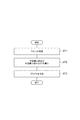
以下、上述したプラズマ処理装置10を用いて実施されるプラズマ処理方法について説明する。図7は、一実施形態に係るプラズマ処理方法を示す流れ図である。図7に示すように、この方法では、まず、工程ST1において、ウエハWが準備される。具体的には、ウエハWが載置台20上に載置され、静電チャックESCによって吸着される。そして、排気装置30が作動されることにより、処理容器12内の空間の圧力が所定の圧力に設定される。次いで、工程ST2において、処理容器12内に中央導入部50及び周辺導入部52からガスが導入される。次いで、工程ST3において、処理容器12内に導入されたガスのプラズマが生成される。このガスのプラズマによってウエハWが処理される。
Hereinafter, the plasma processing method implemented using the
一実施形態においては、ウエハWの処理対象の膜は、シリコン、ゲルマニウム、又はシリコンゲルマニウムから構成された膜である。この実施形態のウエハWを処理する場合には、ガスは、当該膜に対する腐食性を有するガスを含む。例えば、多結晶シリコン膜が処理対象の膜である場合には、当該ガスは、HBrガスを含む。また、当該ガスは、希ガス、及び/又は酸素ガスを更に含み得る。 In one embodiment, the film to be processed of the wafer W is a film made of silicon, germanium, or silicon germanium. When processing the wafer W of this embodiment, the gas includes a gas having corrosiveness to the film. For example, when a polycrystalline silicon film is a film to be processed, the gas includes HBr gas. In addition, the gas may further include a rare gas and / or an oxygen gas.
以上説明したプラズマ処理装置10を用いたプラズマ処理方法によれば、ウエハW上でガスが滞留しないので、ウエハWの膜の処理の面内均一性が向上される。
According to the plasma processing method using the
以下、プラズマ処理装置10の評価のために行ったシミュレーションについて説明する。このシミュレーションでは、載置台20の上面から5mm上方で、軸線Zに対して放射方向のガス流の速度を算出した。また、このシミュレーションでは、以下の条件を模擬した。なお、ガス吐出口52iの角度θが正の値であることは、ガス吐出口52iが斜め上方に延びていることを示しており、ガス吐出口52iの角度θが負の値であることは、ガス吐出口52iが斜め下方に延びていることを示している。
<シミュレーションの条件>
・処理容器12の側壁12aの直径:540mm
・周辺導入部52の載置台20の上面からの距離:90mm
・載置台20の上面と誘電体窓18の平坦面180との間の距離:245mm
・処理ガス:1000sccmのAr、800sccmのHBr
・中央導入部50のガス流量:周辺導入部52のガス流量=70:30
・処理容器12内の圧力:100mTorr(13.33Pa)
・ガス吐出口52iの角度θ:60度、45度、30度、15度、0度、−45度の6種
Hereinafter, a simulation performed for evaluating the
<Simulation conditions>
-Diameter of the
-Distance from the upper surface of the mounting table 20 of the peripheral introduction part 52: 90 mm
The distance between the upper surface of the mounting table 20 and the
Process gas: 1000 sccm Ar, 800 sccm HBr
-Gas flow rate of the central introduction part 50: Gas flow rate of the
-Pressure in the processing vessel 12: 100 mTorr (13.33 Pa)
The angle θ of the
図8は、シミュレーション結果を示す図である。図8の(a)、(b)、(c)、(d)、(e)、(f)はそれぞれ、ガス吐出口52iの角度θが60度、45度、30度、15度、0度、−45度の場合のシミュレーション結果のグラフが示されている。図8の各グラフにおいて、横軸は、軸線Zからの放射方向の距離を示しており、縦軸は、軸線Zに対して放射方向のガス流の速度を示している。
FIG. 8 is a diagram showing a simulation result. 8 (a), (b), (c), (d), (e), and (f), the angle θ of the
図8の(f)に示すように、ガス吐出口52iの角度θが−45度である場合、即ち、ガス吐出口52iが斜め下方に延びている場合には、速度が負の値を有する領域が発生している。このことは、ウエハW上においてガスが滞留する領域が発生することを表している。また、図8の(e)に示すように、ガス吐出口52iの角度θが0度である場合にも、速度が極小値をもつ領域が放射方向の途中に発生している。このことも、ウエハW上においてガスが滞留する領域が発生することを表している。一方、図8の(a)、(b)、(c)及び(d)に示すように、ガス吐出口52iの角度θが60度、45度、30度、15度である場合には、速度は軸線Zから放射方向に離れるにつれて滑らかに減少している。このことから、ガス吐出口52iが斜め上方に延びている場合には、ウエハW上でのガスの滞留が抑制されることが確認された。
As shown in FIG. 8F, when the angle θ of the
次いで、プラズマ処理装置10を用いて行った実験例1、及び比較実験例1〜2について説明する。実験例1では、プラズマ処理装置10を用いて、図9の(a)に示す構造100を、ウエハWに作成した。具体的に、構造100は、基板102、シリコン酸化膜104、フィン106、多結晶シリコン製の複数の領域108、及びシリコン窒化膜製のマスク110を有している。シリコン酸化膜104は、基板102上に設けられている。フィン106は、多結晶シリコンを含んでおり、略直方体形状を有している。複数の領域108は、シリコン酸化膜104上においてフィン106に跨るように設けられている。複数の領域108は、略直方体形状を有しており、互いに平行に延在している。また、マスク110は領域108上に設けられている。実験例1では、この構造100を作成するために、シリコン酸化膜104及びフィン106を覆うように多結晶シリコン層を形成し、当該多結晶シリコン層上にマスク110を設け、プラズマ処理装置10を用いて多結晶シリコン層をエッチングすることにより、領域108を形成した。
Next, Experimental Example 1 performed using the
実験例1の条件は以下の通りであった。
<実験例1の条件>
・処理容器12の側壁12aの直径:540mm
・周辺導入部52の載置台20の上面からの距離:90mm
・載置台20の上面と誘電体窓18の平坦面180との間の距離:245mm
・処理ガス
Arガス:1000sccm
HBrガス:800sccm
Cl2ガス:35sccm
O2ガス:18sccm
・中央導入部50のガス流量:周辺導入部52のガス流量=70:30
・処理容器12内の圧力:120mTorr(16Pa)
・ガス吐出口52iの角度θ:45度
・マイクロ波:2.45GHz、1500W
・高周波バイアス電力:13.56MHz、300W
The conditions of Experimental Example 1 were as follows.
<Conditions of Experimental Example 1>
-Diameter of the
-Distance from the upper surface of the mounting table 20 of the peripheral introduction part 52: 90 mm
The distance between the upper surface of the mounting table 20 and the
・ Processing gas Ar gas: 1000sccm
HBr gas: 800sccm
Cl2 gas: 35 sccm
O 2 gas: 18 sccm
-Gas flow rate of the central introduction part 50: Gas flow rate of the
-Pressure in the processing vessel 12: 120 mTorr (16 Pa)
・ An angle θ of the
・ High frequency bias power: 13.56 MHz, 300 W
比較実験例1及び2では、実験例1と同様に構造100を作成した。但し、比較実験例1ではガス吐出口52iの角度θを−45度とし、比較実験例2ではガス吐出口52iの角度θを0度とした。
In Comparative Experimental Examples 1 and 2, the
そして、実験例1及び比較実験例1〜2で作成した構造100のフィン106と領域108の境界での当該領域108の幅CDを、図9の(b)に示すように、ウエハWの中心からエッジまでを等しく分割した七つの区画C1、T1、T2、T3、T4、T5、及びT6のそれぞれにおいて測定した。
Then, the width CD of the
図10は、実験結果を示す図であり、実験例1及び比較実験例1〜2で作成した構造100の幅CDを示すグラフである。図10に示すグラフにおいて、横軸は、上述した七つの区画を示しており、縦軸はCDを示している。図10に示すように、比較実験例1及び比較実験例2では、区画T3、T4、及びT5のCDが他の区画のCDよりも大きくなっていた。この結果から、比較実験例1及び比較実験例2では、区画T3、T4、及びT5の上方でガスが滞留していたことによるものと推測される。一方、実験例1では、全ての区画のCDの差異が略等しい値になっていた。この結果から、周辺導入部52から斜め上方にガスを吐出することにより、ウエハW上でのガスの滞留を抑制することができ、ウエハWの処理の面内均一性を向上することが可能であることが確認された。
FIG. 10 is a graph showing the experimental results, and is a graph showing the width CD of the
以上、種々の実施形態について説明してきたが、上述した実施形態に限定されることなく種々の変形態様を構成可能である。例えば、プラズマ処理装置10は、プラズマ源としてマイクロ波を利用してガスを励起させるものであった。しかしながら、プラズマ処理装置は、任意のプラズマ源を有し得る。例えば、プラズマ処理装置は、容量結合型のプラズマ処理装置であってもよく、誘導結合型のプラズマ処理装置であってもよい。
Although various embodiments have been described above, various modifications can be made without being limited to the above-described embodiments. For example, the
10…プラズマ処理装置、12…処理容器、12a…側壁、14…アンテナ、18…誘電体窓、20…載置台、ESC…静電チャック、LE…下部電極、30…排気装置、32…マイクロ波発生器、50…中央導入部、18i…ガス吐出口、52…周辺導入部、52p…環状の管、52i…ガス吐出口、VL…排気路、VP…仮想面、θ…周辺導入部のガス吐出口の角度、Z…軸線。
DESCRIPTION OF
Claims (7)
側壁を有する処理容器と、
前記処理容器内に設けられた載置台と、
前記載置台の上方に設けられた中央導入部であり、前記載置台の中心を通る軸線に沿って前記載置台に向けてガスを導入する中央導入部と、
前記軸線が延在する方向において前記中央導入部と前記載置台の上面との間に設けられており、且つ、前記側壁に沿って設けられた周辺導入部であり、前記軸線に対して周方向に配列された複数のガス吐出口を提供する、該周辺導入部と、
を備え、
前記複数のガス吐出口は、前記軸線に近づくにつれて前記該載置台から離れるように延びている、
プラズマ処理装置。 A plasma processing apparatus for performing plasma processing on an object to be processed,
A processing vessel having a side wall;
A mounting table provided in the processing container;
A central introduction part provided above the mounting table, and a central introduction part for introducing gas toward the mounting table along an axis passing through the center of the mounting table;
A peripheral introduction portion provided between the central introduction portion and the upper surface of the mounting table in a direction in which the axis extends, and provided along the side wall; and circumferential direction with respect to the axis Providing a plurality of gas outlets arranged in the peripheral introduction portion;
With
The plurality of gas discharge ports extend away from the mounting table as approaching the axis.
Plasma processing equipment.
前記アンテナは、前記載置台の上方において前記載置台と対面するように設けられており、且つ、前記処理容器内の空間に接する誘電体窓を有し、
前記誘電体窓には前記軸線に沿って延びる前記中央導入部のガス吐出口が形成されている、請求項1又は2に記載のプラズマ処理装置。 An antenna for introducing microwaves into the processing vessel;
The antenna is provided to face the mounting table above the mounting table, and has a dielectric window in contact with the space in the processing container,
3. The plasma processing apparatus according to claim 1, wherein a gas discharge port of the central introduction portion extending along the axis is formed in the dielectric window.
前記中央導入部及び前記周辺導入部からガスを導入し、該ガスのプラズマにより前記載置台上に載置された被処理体を処理するプラズマ処理方法。 A plasma processing method using the plasma processing apparatus according to any one of claims 1 to 4,
A plasma processing method for introducing a gas from the central introduction part and the peripheral introduction part, and treating a target object placed on the mounting table by plasma of the gas.
前記ガスは、前記膜に対して腐食性を有するガスを含む、
請求項5に記載のプラズマ処理方法。 The object to be processed has a film made of silicon, germanium, or silicon germanium,
The gas includes a gas that is corrosive to the film.
The plasma processing method according to claim 5.
Priority Applications (3)
| Application Number | Priority Date | Filing Date | Title |
|---|---|---|---|
| JP2014080213A JP2015201567A (en) | 2014-04-09 | 2014-04-09 | plasma processing apparatus and method |
| US14/681,161 US20150294839A1 (en) | 2014-04-09 | 2015-04-08 | Plasma processing apparatus and plasma processing method |
| KR1020150050226A KR20150117227A (en) | 2014-04-09 | 2015-04-09 | Plasma processing apparatus and plasma processing method |
Applications Claiming Priority (1)
| Application Number | Priority Date | Filing Date | Title |
|---|---|---|---|
| JP2014080213A JP2015201567A (en) | 2014-04-09 | 2014-04-09 | plasma processing apparatus and method |
Publications (1)
| Publication Number | Publication Date |
|---|---|
| JP2015201567A true JP2015201567A (en) | 2015-11-12 |
Family
ID=54265658
Family Applications (1)
| Application Number | Title | Priority Date | Filing Date |
|---|---|---|---|
| JP2014080213A Withdrawn JP2015201567A (en) | 2014-04-09 | 2014-04-09 | plasma processing apparatus and method |
Country Status (3)
| Country | Link |
|---|---|
| US (1) | US20150294839A1 (en) |
| JP (1) | JP2015201567A (en) |
| KR (1) | KR20150117227A (en) |
Families Citing this family (1)
| Publication number | Priority date | Publication date | Assignee | Title |
|---|---|---|---|---|
| KR20160021958A (en) * | 2014-08-18 | 2016-02-29 | 삼성전자주식회사 | Plasma treating apparatus and substrate treating apparatus |
Family Cites Families (8)
| Publication number | Priority date | Publication date | Assignee | Title |
|---|---|---|---|---|
| US6185839B1 (en) * | 1998-05-28 | 2001-02-13 | Applied Materials, Inc. | Semiconductor process chamber having improved gas distributor |
| US20060042754A1 (en) * | 2004-07-30 | 2006-03-02 | Tokyo Electron Limited | Plasma etching apparatus |
| US7250373B2 (en) * | 2004-08-27 | 2007-07-31 | Applied Materials, Inc. | Method and apparatus for etching material layers with high uniformity of a lateral etch rate across a substrate |
| KR20060076346A (en) * | 2004-12-29 | 2006-07-04 | 주식회사 하이닉스반도체 | High Density Plasma Chemical Vapor Deposition Equipment for Semiconductor Manufacturing |
| KR101341371B1 (en) * | 2008-11-18 | 2013-12-13 | 도쿄엘렉트론가부시키가이샤 | Plasma processing device and plasma processing method |
| CN102473634B (en) * | 2009-08-20 | 2015-02-18 | 东京毅力科创株式会社 | Plasma treatment device and plasma treatment method |
| US8415884B2 (en) * | 2009-09-08 | 2013-04-09 | Tokyo Electron Limited | Stable surface wave plasma source |
| KR101772723B1 (en) * | 2010-06-28 | 2017-08-29 | 도쿄엘렉트론가부시키가이샤 | Plasma processing method |
-
2014
- 2014-04-09 JP JP2014080213A patent/JP2015201567A/en not_active Withdrawn
-
2015
- 2015-04-08 US US14/681,161 patent/US20150294839A1/en not_active Abandoned
- 2015-04-09 KR KR1020150050226A patent/KR20150117227A/en not_active Withdrawn
Also Published As
| Publication number | Publication date |
|---|---|
| KR20150117227A (en) | 2015-10-19 |
| US20150294839A1 (en) | 2015-10-15 |
Similar Documents
| Publication | Publication Date | Title |
|---|---|---|
| KR102356211B1 (en) | Etching method | |
| JP6154390B2 (en) | Electrostatic chuck | |
| CN110047775B (en) | Semiconductor device manufacturing apparatus and method | |
| TWI686863B (en) | Method for etching organic film | |
| JP6974088B2 (en) | Plasma processing equipment and plasma processing method | |
| JP6339961B2 (en) | Etching method | |
| KR102348077B1 (en) | Plasma processing method | |
| CN102217044A (en) | Plasma processing device and plasma processing method | |
| KR20210037318A (en) | Substrate processing apparatus and method, and semiconductor device manufacturing method using the processing method | |
| KR20200051505A (en) | Placing table and substrate processing apparatus | |
| TW202027161A (en) | Method for etching, and plasma processing device | |
| TWI650812B (en) | Method for etching ruthenium layer, and plasma processing device | |
| KR102183566B1 (en) | Etching method | |
| JP2019201086A (en) | Processing device, component, and temperature control method | |
| WO2020059596A1 (en) | Placement table and substrate treating device | |
| KR102185192B1 (en) | Plasma etching method | |
| CN105027269B (en) | The productivity ratio of etch system is improved by polymer management | |
| KR20190114870A (en) | Plasma processing apparatus | |
| JP2019102521A (en) | Component for semiconductor manufacturing device and semiconductor manufacturing device | |
| JP2015201567A (en) | plasma processing apparatus and method | |
| US9711371B2 (en) | Method of etching organic film | |
| CN110660721B (en) | Wafer bearing device, system and method | |
| JP2022023211A (en) | Plasma processing device and plasma processing method | |
| KR20230127373A (en) | Method for processing workpiece | |
| JP6308858B2 (en) | Electrostatic chuck, mounting table, plasma processing equipment |
Legal Events
| Date | Code | Title | Description |
|---|---|---|---|
| A621 | Written request for application examination |
Free format text: JAPANESE INTERMEDIATE CODE: A621 Effective date: 20161222 |
|
| A761 | Written withdrawal of application |
Free format text: JAPANESE INTERMEDIATE CODE: A761 Effective date: 20170412 |