JP2015200765A - Light-emitting element display device - Google Patents
Light-emitting element display device Download PDFInfo
- Publication number
- JP2015200765A JP2015200765A JP2014079178A JP2014079178A JP2015200765A JP 2015200765 A JP2015200765 A JP 2015200765A JP 2014079178 A JP2014079178 A JP 2014079178A JP 2014079178 A JP2014079178 A JP 2014079178A JP 2015200765 A JP2015200765 A JP 2015200765A
- Authority
- JP
- Japan
- Prior art keywords
- reflective electrode
- light
- emitting element
- display device
- layer
- Prior art date
- Legal status (The legal status is an assumption and is not a legal conclusion. Google has not performed a legal analysis and makes no representation as to the accuracy of the status listed.)
- Pending
Links
- 239000010410 layer Substances 0.000 claims abstract description 80
- 239000000758 substrate Substances 0.000 claims abstract description 40
- 239000012044 organic layer Substances 0.000 claims abstract description 17
- 239000004020 conductor Substances 0.000 claims abstract description 10
- 239000011159 matrix material Substances 0.000 claims abstract description 7
- 239000011368 organic material Substances 0.000 claims abstract description 5
- 239000004983 Polymer Dispersed Liquid Crystal Substances 0.000 claims description 29
- 239000003990 capacitor Substances 0.000 claims description 11
- 239000004973 liquid crystal related substance Substances 0.000 abstract description 9
- 239000004815 dispersion polymer Substances 0.000 abstract description 5
- 238000010586 diagram Methods 0.000 description 17
- 230000004048 modification Effects 0.000 description 12
- 238000012986 modification Methods 0.000 description 12
- 239000010408 film Substances 0.000 description 10
- 230000005684 electric field Effects 0.000 description 9
- 239000003086 colorant Substances 0.000 description 7
- 230000005540 biological transmission Effects 0.000 description 5
- 239000011347 resin Substances 0.000 description 4
- 229920005989 resin Polymers 0.000 description 4
- 238000007789 sealing Methods 0.000 description 4
- 230000000694 effects Effects 0.000 description 3
- 238000005401 electroluminescence Methods 0.000 description 3
- 238000005286 illumination Methods 0.000 description 3
- 238000000926 separation method Methods 0.000 description 3
- 230000007423 decrease Effects 0.000 description 2
- 239000006185 dispersion Substances 0.000 description 2
- 239000011810 insulating material Substances 0.000 description 2
- 238000004519 manufacturing process Methods 0.000 description 2
- 239000000463 material Substances 0.000 description 2
- 238000010521 absorption reaction Methods 0.000 description 1
- 239000003795 chemical substances by application Substances 0.000 description 1
- 230000002542 deteriorative effect Effects 0.000 description 1
- 238000009792 diffusion process Methods 0.000 description 1
- 239000011521 glass Substances 0.000 description 1
- AMGQUBHHOARCQH-UHFFFAOYSA-N indium;oxotin Chemical compound [In].[Sn]=O AMGQUBHHOARCQH-UHFFFAOYSA-N 0.000 description 1
- 238000009413 insulation Methods 0.000 description 1
- 230000031700 light absorption Effects 0.000 description 1
- 238000000034 method Methods 0.000 description 1
- 239000000565 sealant Substances 0.000 description 1
- 239000010409 thin film Substances 0.000 description 1
- 238000002834 transmittance Methods 0.000 description 1
Images


Abstract
Description
本発明は、発光素子表示装置に関する。 The present invention relates to a light emitting element display device.
近年、有機発光ダイオード(OLED:Organic Light Emitting Diode)等の自発光体を用いた発光素子表示装置が実用化されている。このようなOLEDを用いた有機EL(Electro-luminescent)表示装置をはじめとする発光素子表示装置は、従来の液晶表示装置と比較して、自発光体を用いているため、視認性、応答速度の点で優れているだけでなく、バックライトのような補助照明装置を要しないため、更なる薄型化が可能となっている。 2. Description of the Related Art In recent years, light emitting element display devices using self-luminous materials such as organic light emitting diodes (OLEDs) have been put into practical use. Light-emitting element display devices such as organic EL (Electro-luminescent) display devices using such OLEDs use a self-luminous body as compared with conventional liquid crystal display devices, so that visibility and response speed are improved. In addition to being excellent in this respect, since an auxiliary lighting device such as a backlight is not required, further thinning is possible.
特許文献1は、PDLC(Polymer Dispersed Liquid Crystal:高分子分散型液晶)層を有する有機EL表示装置において、発光素子が発光している状態においてPDLC層が透明性を示し、発光素子が発光していない状態においてPDLC層が光吸収性を示すように制御される有機EL表示装置について開示している。 Patent Document 1 discloses that in an organic EL display device having a PDLC (Polymer Dispersed Liquid Crystal) layer, the PDLC layer shows transparency when the light emitting element emits light, and the light emitting element emits light. An organic EL display device is disclosed in which the PDLC layer is controlled so as to exhibit light absorption in the absence of the PDLC layer.
特許文献2は、有機エレクトロルミネッセンス素子において、有機発光層に接する電極の基板側に、散乱層及び吸収電極を設け、有機発光層が発光していない状態で散乱層は散乱性を有せず、有機発光層が発光している状態で散乱層は散乱性を有している有機エレクトロルミネッセンス素子について開示している。 In Patent Document 2, in the organic electroluminescence element, a scattering layer and an absorption electrode are provided on the substrate side of the electrode in contact with the organic light emitting layer, and the scattering layer does not have scattering properties in a state where the organic light emitting layer is not emitting light. An organic electroluminescence device is disclosed in which the scattering layer has a scattering property while the organic light emitting layer emits light.
有機EL表示装置は、観察者側からみて発光層の裏側に通常、発光効率を高めるための反射膜を有しているが、例えば室外等において外光が強い場合には、反射膜による外光の反射により画像の視認性が悪化したり、画面上に虹模様が発生することがあった。従来、このような外光反射の防止のために、円偏光板を表示パネルの上面に設置する構造が提案されているが、円偏光板の光透過率は50%未満と低く、発光効率の低下につながることとなっていた。また、円偏光板の追加は、新たな製造工程を増加させることとなるため、製造コストの上昇にも繋がる恐れがあった。 The organic EL display device usually has a reflective film on the back side of the light-emitting layer as viewed from the observer side. However, for example, when the outside light is strong outside the room, the external light from the reflective film is used. Due to the reflection, the visibility of the image may deteriorate or a rainbow pattern may occur on the screen. Conventionally, in order to prevent such reflection of external light, a structure in which a circularly polarizing plate is installed on the upper surface of the display panel has been proposed, but the light transmittance of the circularly polarizing plate is as low as less than 50%, and the luminous efficiency is low. It was supposed to lead to a decline. Moreover, since the addition of a circularly polarizing plate increases a new manufacturing process, it may lead to an increase in manufacturing cost.
本発明は上述の事情を鑑みてしたものであり、外光の環境が変化した場合であっても高い視認性で表示させることができる発光素子表示装置を提供することを目的とする。 The present invention has been made in view of the above circumstances, and an object thereof is to provide a light-emitting element display device that can display with high visibility even when the environment of external light changes.
本発明の発光素子表示装置は、マトリクス状に配置された複数の画素からなる表示領域を有する基板と、前記基板上の前記複数の画素のそれぞれにおいて形成され、導電体からなる下部電極と、前記下部電極上に形成され、有機材料からなる発光層を含む有機層と、前記有機層上に形成され、導電体からなる上部電極と、前記下部電極より前記基板側に形成され、前記表示領域の各画素において共通の電位を有する反射電極層と、前記下部電極及び前記反射電極層の間に配置される高分子分散型液晶層と、周囲環境の光の強さを測定する外光センサと、前記外光センサの出力に基づいて前記反射電極層に印加する電位を変化させる反射電極制御部と、を備えることを特徴とする発光素子表示装置である。 The light-emitting element display device of the present invention includes a substrate having a display region composed of a plurality of pixels arranged in a matrix, a lower electrode made of a conductor and formed in each of the plurality of pixels on the substrate, An organic layer formed on the lower electrode and including a light emitting layer made of an organic material; an upper electrode formed on the organic layer and made of a conductor; and formed on the substrate side of the lower electrode; A reflective electrode layer having a common potential in each pixel; a polymer-dispersed liquid crystal layer disposed between the lower electrode and the reflective electrode layer; an external light sensor that measures the intensity of light in the surrounding environment; A light emitting element display device comprising: a reflective electrode control unit that changes a potential applied to the reflective electrode layer based on an output of the external light sensor.
本発明の発光素子表示装置は、マトリクス状に配置された複数の画素からなる表示領域を有する基板と、前記基板上の前記複数の画素のそれぞれにおいて形成され、導電体からなる下部電極と、前記下部電極上に形成され、有機材料からなる発光層を含む有機層と、前記有機層上に形成され、導電体からなる上部電極と、前記下部電極より前記基板側に形成された反射電極層と、前記下部電極及び前記反射電極層の間に配置される高分子分散型液晶層と、を備え、前記反射電極層及び前記下部電極は電気容量を形成する、ことを特徴とする発光素子表示装置である。 The light-emitting element display device of the present invention includes a substrate having a display region composed of a plurality of pixels arranged in a matrix, a lower electrode made of a conductor and formed in each of the plurality of pixels on the substrate, An organic layer formed on the lower electrode and including a light emitting layer made of an organic material; an upper electrode formed on the organic layer and made of a conductor; and a reflective electrode layer formed on the substrate side from the lower electrode; And a polymer dispersed liquid crystal layer disposed between the lower electrode and the reflective electrode layer, wherein the reflective electrode layer and the lower electrode form a capacitance. It is.
ここで、「画素」は、発光素子を有する単位を意味し、画素が複数の発光素子で構成されることにより複数の副画素を有している場合には副画素を意味する。 Here, the “pixel” means a unit having a light-emitting element, and means a sub-pixel when the pixel includes a plurality of light-emitting elements and thus has a plurality of sub-pixels.
また、本発明の発光素子表示装置において、前記反射電極層は、表示領域の各画素において共通の電位を有することとしてもよい。 In the light emitting element display device of the present invention, the reflective electrode layer may have a common potential in each pixel of the display region.
また、本発明の発光素子表示装置において、階調電圧に基づく電位が印加されることにより前記発光層における発光を制御する駆動トランジスタを更に備え、前記反射電極層は、前記駆動トランジスタのゲートに電気的に接続されていてもよい。また、この場合には、前記画素毎に形成されたスイッチを介して、前記反射電極層に電気的に接続される反射電極制御線を更に備えていてもよい。更に、この場合には、前記高分子分散型液晶層は、前記駆動トランジスタのゲート及び前記発光素子のアノード間の電位を保持する保持容量であってもよい。 The light-emitting element display device according to the present invention further includes a drive transistor that controls light emission in the light-emitting layer by applying a potential based on a gradation voltage, and the reflective electrode layer is electrically connected to a gate of the drive transistor. May be connected to each other. In this case, a reflective electrode control line electrically connected to the reflective electrode layer may be further provided via a switch formed for each pixel. Further, in this case, the polymer dispersed liquid crystal layer may be a storage capacitor that holds a potential between the gate of the driving transistor and the anode of the light emitting element.
また、本発明の発光素子表示装置において、前記反射電極層に印加する電位を変化させる反射電極制御部を更に備えていてもよい。この場合には、周囲環境の光の強さを測定する外光センサを更に備え、前記反射電極制御部は、前記外光センサの出力に基づいて前記反射電極層に印加する電位を変化させてもよい。 The light emitting element display device of the present invention may further include a reflective electrode control unit that changes a potential applied to the reflective electrode layer. In this case, it further includes an external light sensor that measures the intensity of light in the surrounding environment, and the reflective electrode control unit changes the potential applied to the reflective electrode layer based on the output of the external light sensor. Also good.
以下に、本発明の各実施の形態について、図面を参照しつつ説明する。なお、開示はあくまで一例にすぎず、当業者において、発明の主旨を保っての適宜変更について容易に想到し得るものについては、当然に本発明の範囲に含有されるものである。また、図面は説明をより明確にするため、実際の態様に比べ、各部の幅、厚さ、形状等について模式的に表される場合があるが、あくまで一例であって、本発明の解釈を限定するものではない。また、本明細書と各図において、既出の図に関して前述したものと同様の要素には、同一の符号を付して、詳細な説明を適宜省略することがある。 Hereinafter, embodiments of the present invention will be described with reference to the drawings. It should be noted that the disclosure is merely an example, and those skilled in the art can easily conceive of appropriate modifications while maintaining the gist of the invention are naturally included in the scope of the present invention. In addition, the drawings may be schematically represented with respect to the width, thickness, shape, and the like of each part in comparison with actual aspects for the sake of clarity of explanation, but are merely examples, and the interpretation of the present invention is not limited. It is not limited. In addition, in the present specification and each drawing, elements similar to those described above with reference to the previous drawings are denoted by the same reference numerals, and detailed description may be omitted as appropriate.
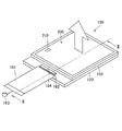
図1には、本発明の実施形態に係る発光素子表示装置である有機EL表示装置100が概略的に示されている。この図に示されるように、有機EL表示装置100は、TFT(Thin Film Transistor:薄膜トランジスタ)基板120及び対向基板150の2枚の基板を有している。有機EL表示装置100のTFT基板120及び対向基板150には、マトリクス状に配置された画素210からなる表示領域205が形成されている。ここで、各画素210は複数の副画素212(後述)から構成されている。
FIG. 1 schematically shows an organic
また、TFT基板120は透明のガラス又は樹脂の絶縁材料からなる基板であり、TFT基板120には、副画素212のそれぞれに配置された画素トランジスタの走査信号線に対してソース・ドレイン間を導通させるための電位を印加すると共に、画像信号線に対して副画素212の階調値に対応する電圧を印加する駆動回路である駆動IC(Integrated Circuit)182が載置され、外部から画像信号等を入力するためのFPC(Flexible Printed Circuits)181が取付けられている。また、有機EL表示装置100の環境における外光照度について測定する外光センサである照度センサ(輝度センサ)183を有していてもよく、この場合には照度センサ183の出力が、直接又は間接的に駆動IC182に通知される。更に、駆動IC182内には、照度センサ183の出力又は使用者の指示に基づいて表示品質を制御する反射電極制御部184を有している。ここで照度センサ等の外光センサは、発光素子表示装置を備える端末装置等に内蔵されたカメラや環境光センサとすることができる。なお、本実施形態においては、図の矢印に示されるように、TFT基板120の発光層が形成された側に光を出射するトップエミッション型の有機EL表示装置としている。
The
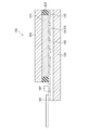
図2は、図1のII−II線における断面を概略的に示す図である。この断面図に示されるように、TFT基板120には、TFT回路が形成されたTFT回路層160と、TFT回路層160上に形成された複数の発光素子である複数の有機EL素子OLEDと、有機EL素子OLEDを覆って水分を遮断する封止膜125と、を有している。有機EL素子OLEDは、各画素210に含まれる副画素212の数だけ形成されるが、図2では説明を分かりやすくするため、省略して記載している。また、対向基板150には、例えば3色又は4色のそれぞれ異なる波長領域の光を透過するカラーフィルタ及び各副画素212の境界から出射される光を遮断する遮光膜であるブラックマトリクスが形成されている。TFT基板120と対向基板150との間の透明樹脂221は、シール剤222により封止されている。
FIG. 2 is a diagram schematically showing a cross section taken along line II-II in FIG. As shown in this cross-sectional view, the
なお、本実施形態においては、駆動IC182をTFT基板120上に配置することとしたが、駆動IC182をFPC181上に配置することとしてもよく、また、駆動回路はTFT基板120上に直接形成されることとしてもよい。また、TFT基板120を柔軟な樹脂材料とし、対向基板150を有さない構成とすることもでき、この場合には、TFT基板120をFPC181と一体とした構成であってもよい。また、本実施形態においては、有機EL素子OLEDにおいて白色を発光し、カラーフィルタを用いて3色又は4色の波長領域の光を透過する構成とするが、有機EL素子OLEDにおいて、例えば3色又は4色のそれぞれ異なる波長領域の光を発光する構成としてもよい。
In the present embodiment, the driving
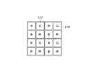
図3は、図1の画素210に含まれる副画素212の構成例について示す図である。この図に示されるように画素210は、R(赤)G(緑)B(青)W(白)の4種類の色に対応する波長領域の光を出射する略矩形の副画素212からなり、副画素212は同じ画素210内の他の副画素212と2辺が接するように田の字型に整列されている。なお、画素210における副画素212の構成は、図3の構成に限られず、図4に示されるようなRGBの3色に対応する副画素212からなるストライプ構成であってもよく、また、ストライプ構成で更にRGBWの4種類の色を使用するものであってもよい。画素210を構成する副画素212の配置はこれらに限られず適宜定めることができる。
FIG. 3 is a diagram illustrating a configuration example of the sub-pixel 212 included in the
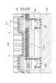
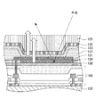
図5は、副画素212のTFT基板120側の断面の一例について拡大して示す図である。この図に示されるように、TFT回路層160内の駆動トランジスタDRTのソース/ドレインの一方は、例えばITO(Indium Tin Oxide)やAg等からなり、副画素212毎に独立した下部電極131に接続されている。下部電極131の端部は、隣接する副画素212の下部電極131と絶縁性を保つための、絶縁材料からなる画素分離膜137に覆われており、画素分離膜137上と、下部電極131上で表示領域205を覆うように発光層を含む有機層133が成膜されている。更に、下部電極131と対となって発光層を発光させるための上部電極135が、ITO等の透明電極により形成されている。上部電極135上には、有機層133の劣化を防ぐために、空気の侵入を防ぐ封止膜125が表示領域205を覆うように形成されている。また下部電極131の基板120側には、下部電極131に平行なAg等からなる反射電極138が形成され、発光層において発光した光を表示面側に反射させている。また、反射電極138と下部電極131との間には、高分子分散型液晶からなる高分子分散型液晶層139が配置されている。ここで高分子分散型液晶は、反射電極138と下部電極131に電位差が生じ、電界が生じている場合には可視光を透過する透過状態となり、反射電極138と下部電極131に電位差がなく電界が発生していない場合には入射する光を散乱させる散乱状態となる性質を有している。また電界の大きさに応じ、これらの中間状態となることも可能である。
FIG. 5 is an enlarged view showing an example of a cross section of the
各副画素212においては、下部電極131と接続された駆動トランジスタDRTが、各副画素212の階調電圧を反映した電流を流し、共通の電位に保たれた上部電極135と下部電極131との間の有機層133内の発光層を発光させる。有機層133は、上部電極135から出射される光が共振効果を利用して光が強められるように調整された膜厚を有する、所謂マイクロキャビティ効果を利用したものとすることができる。このマイクロキャビティ効果を利用する場合には特に正面輝度が高くなるように調整することができる。
In each
なお、本実施形態では、有機層133は表示領域205を覆う層であることとし、各副画素212において、例えばW(白)等の発光を行うこととしているが、各副画素212毎に発光層を塗り分け、各画素210において異なる色の波長領域の光を発する副画素212を有する構成としていてもよい。
In the present embodiment, the
なお、反射電極138への電位の印加は、図1の反射電極制御部184を介して行われ、表示領域の外側の複数の箇所において配線と接触することにより、各副画素212の反射電極138に共通で均一な電位を印加させることができる。なお、図1では反射電極制御部184を駆動IC182内に設けることとしているが、駆動IC182以外の制御回路内に設けることとしてもよい。また、反射電極制御部184への指示は、手動により、つまり画面表示の設定機能を提供する画面等からタッチパネル等の入力装置を用いて行われることとしてもよいし、図1の照度センサ183の出力を用いて切替えることとしてもよい。この場合に透過状態と散乱状態と2段階だけでなく、印加する電圧を3段階以上又は無段階で連続的に切り替えることにより、透過状態と散乱状態との間を3段階以上又は無段階で連続的に切り替わることとしてもよい。また、表示領域205内の各反射電極138は共通の電位でなく、個別に異なる電位であってもよく、更に反射電極制御部184を用いない構成としてもよい。
Note that application of a potential to the
図6及び7は、図5の構成における外光反射に対する制御を説明するための図であり、図6は、外光が弱いときの制御について説明するための図である。この図に示されるように、外光が弱いとき、例えば、照度センサ183からの出力に基づいて反射電極制御部184が外光が弱いと判定したときには、反射電極制御部184は、反射電極138に下部電極131との間に電位差を生じさせるような電圧を印加する。これにより反射電極138と下部電極131との間に生成された電界により、高分子分散型液晶層139は透過状態となる。このため、発光層で発光し基板120側へ向う光は、高分子分散型液晶層139を透過し、反射電極138で反射した後、再び高分子分散型液晶層139を透過して出射される。したがって、外光が弱いと判定された場合には、発光層で発光した光を反射を利用して効率よく出射させて、コントラストを高め視認性を向上させることができる。
6 and 7 are diagrams for explaining control with respect to external light reflection in the configuration of FIG. 5, and FIG. 6 is a diagram for explaining control when external light is weak. As shown in this figure, when the external light is weak, for example, when the reflective
図7は、外光が強いときの制御について説明するための図である。この図に示されるように、外光が強いとき、例えば、照度センサ183からの出力に基づいて反射電極制御部184が外光が強いと判定したときには、反射電極制御部184は、反射電極138に下部電極131と同電位又は同電位に近くなるような電位を印加する。これにより反射電極138と下部電極131との間には電界がほとんど発生せず、高分子分散型液晶層139は散乱状態となる。これにより表示面の外から反射電極138に向う外光は高分子分散型液晶層139で散乱され、ほとんど反射されることがないため、発光層で発光して外に向う光を妨げない。したがって、外光が強いと判定された場合には、反射電極138における外光の反射を抑え、視認性を向上させることができる。
FIG. 7 is a diagram for explaining control when external light is strong. As shown in this figure, when the external light is strong, for example, when the reflective
なお、本実施形態においては、照度センサ183による出力において、外光が強いと判定される場合には高分子分散型液晶層139を散乱状態とし、外光が弱いと判定される場合には高分子分散型液晶層139を透過状態とするように制御することとしたが、逆に外光が強いと判定される場合に散乱状態とし、外光が弱いと判定される場合に透過状態とすることもできる。これは、例えば外光反射を担う反射電極138が外光をどの程度反射するように設計されているか等の設計的要因により影響される。つまり、透過状態及び拡散状態を適切に選択することにより、外光の環境が変化した場合であっても高い視認性で表示させることができる。
In the present embodiment, in the output from the
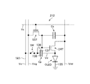
図8は、上述の副画素212の回路の一例について示す回路図である。この図に示されるように、回路は、上部電極135、有機層133及び下部電極131とからなる有機EL素子OLEDと、アノード(下部電極131)側にソース/ドレインの一方が接続され、ソース/ドレインの他方が高基準電位Vddに接続された駆動トランジスタDRTと、駆動トランジスタDRTのゲートに接続され、映像信号電圧Vsigをゲートに印加する行選択スイッチSSTと、駆動トランジスタDRTのゲートとソース/ドレインの他方との間に形成された保持容量Csと、反射電極138が接続された反射電極制御線141と、から構成され、下部電極131と反射電極138とは高分子分散型液晶層139を介して容量Cpを形成している。高分子分散型液晶層139の電界を形成する下部電極131及び反射電極138間の電位差(ΔV=Vd−Vc)は、照度センサ183による出力、又は手動による指示等に基づいて、反射電極制御部184が反射電極電位Vcを変化させることにより制御される。
FIG. 8 is a circuit diagram illustrating an example of the circuit of the sub-pixel 212 described above. As shown in this figure, the circuit includes an organic EL element OLED composed of an
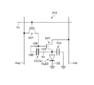
図9は、図8に示された回路の第1変形例について示す回路図である。図8の回路と異なる点は、反射電極138が駆動トランジスタDRTのゲートに接続され、反射電極138と反射電極制御線141とは、スイッチSWを介して接続されている点である。反射電極138に対して映像信号電圧Vsigを印加した上で所望の反射電極電位Vcを重畳する回路となっている。スイッチSWを制御し、映像信号電圧Vsigを書込むタイミングをずらすことで重畳することができる。この回路では、映像信号電圧Vsigは保持容量Csと容量Cpとに蓄積され、大きな容量を確保することができる。
FIG. 9 is a circuit diagram showing a first modification of the circuit shown in FIG. The difference from the circuit of FIG. 8 is that the
図10は、図8に示された回路の第2変形例について示す回路図である。図9の第1変形例の回路から、保持容量Csを削除している点で異なっている。この場合には、図9の回路と同様に制御することができると共に、容量Cpを保持容量Csとして機能させるため、図9において存在していた保持容量Csの分の領域を有効活用することができる。 FIG. 10 is a circuit diagram showing a second modification of the circuit shown in FIG. This is different from the circuit of the first modified example of FIG. 9 in that the storage capacitor Cs is deleted. In this case, the control can be performed in the same manner as the circuit of FIG. 9 and the region corresponding to the storage capacitor Cs existing in FIG. 9 can be effectively used in order to cause the capacitor Cp to function as the storage capacitor Cs. it can.
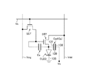
図11は、図8に示された回路の第3変形例について示す回路図である。この例では、反射電極制御線141を有さず、反射電極138が駆動トランジスタDRTのゲートに接続されている。また、駆動トランジスタDRTのソース/ドレインの一方は、例えば、上部電極135の電位等の基準電位と補助容量Cadを形成している。このように構成することにより、反射電極138の制御電位として映像信号電圧Vsigを用いることができる。つまり、各副画素212の発光輝度と連動して高分子分散型液晶層139の拡散性を変化させることができる。この場合において、通常の高分子分散型液晶を用いた場合には、画素の発光輝度が高い場合に高分子分散型液晶層139が透過状態となり、画素の発光輝度が低い場合に高分子分散型液晶層139を散乱状態となる。しかしながら、電位差が大きいほど拡散性が高くなり、電位差が小さいほど透過性が高くなるリバース型の高分子分散型液晶を用いることにより、画素の発光輝度が高い場合に高分子分散型液晶層139を散乱状態とし、画素の発光輝度が低い場合に高分子分散型液晶層139を透過状態とすることができる。
FIG. 11 is a circuit diagram showing a third modification of the circuit shown in FIG. In this example, the reflective
図12は、図8に示された回路の第4変形例について示す回路図である。この例では、第3変形例と同様に反射電極制御線141を有していない。また、駆動トランジスタDRTのソース/ドレインの一方とゲートとで保持容量Csを形成しており、反射電極138は反射電極電位Vcと接続され、補助容量Cadを形成している。この反射電極電位Vcは図8の場合と同様に、照度センサ183による出力、又は手動による指示等に基づいて、反射電極制御部184により制御されることとしてもよい。また、この場合においても上述のリバース型の高分子分散型液晶を用いることができる。
FIG. 12 is a circuit diagram showing a fourth modification of the circuit shown in FIG. In this example, the reflective
また、特に詳述しないが、上述の各回路の制御において、必要に応じて駆動トランジスタDRTの閾値電圧の補正のための動作、及び移動度の補正のための動作を組み合わせることができる。また、上述の特に反射電極電位Vcの制御は2段階に限らず、多段階及び/又は連続的であってもよい。 Although not specifically described in detail, in the control of each circuit described above, the operation for correcting the threshold voltage of the drive transistor DRT and the operation for correcting the mobility can be combined as necessary. Further, the control of the reflection electrode potential Vc described above is not limited to two steps, and may be multi-step and / or continuous.
また、上述の各実施形態における高分子分散型液晶には、図11及び12の場合を除き、電界が発生している場合に透過状態となり、電界が発生していない場合に散乱状態となるノーマルの高分子分散型液晶を用いることとしているが、使用環境や設計条件に応じて、電界が発生している場合に散乱状態となり、電界が発生していない場合に透過状態となるリバース型の高分子分散型液晶を用いることができる。 Further, the polymer dispersed liquid crystal in each of the above-described embodiments has a normal state that is in a transmissive state when an electric field is generated and is in a scattering state when no electric field is generated, except in the cases of FIGS. However, depending on the usage environment and design conditions, a reverse type high-performance liquid crystal that is in a scattering state when an electric field is generated and in a transmission state when no electric field is generated, is used. A molecular dispersion type liquid crystal can be used.
本発明の思想の範疇において、当業者であれば、各種の変更例及び修正例に想到し得るものであり、それら変更例及び修正例についても本発明の範囲に属するものと了解される。例えば、前述の各実施形態に対して、当業者が適宜、構成要素の追加、削除若しくは設計変更を行ったもの、又は、工程の追加、省略若しくは条件変更を行ったものも、本発明の要旨を備えている限り、本発明の範囲に含まれる。 In the scope of the idea of the present invention, those skilled in the art can conceive various changes and modifications, and it is understood that these changes and modifications also belong to the scope of the present invention. For example, those in which the person skilled in the art has appropriately added, deleted, or changed the design of the above-described embodiments, or those in which processes have been added, omitted, or changed conditions are also the subject matter of the present invention. As long as it is included in the scope of the present invention.
100 有機EL表示装置、120 TFT基板、125 封止膜、131 下部電極、133 有機層、135 上部電極、137 画素分離膜、138 反射電極、139 高分子分散型液晶層、141 反射電極制御線、150 対向基板、160 TFT回路層、182 駆動IC、183 照度センサ、184 反射電極制御部、205 表示領域、210 画素、212 副画素、221 透明樹脂、222 シール剤。 100 organic EL display device, 120 TFT substrate, 125 sealing film, 131 lower electrode, 133 organic layer, 135 upper electrode, 137 pixel separation film, 138 reflective electrode, 139 polymer dispersed liquid crystal layer, 141 reflective electrode control line, 150 counter substrate, 160 TFT circuit layer, 182 drive IC, 183 illuminance sensor, 184 reflective electrode control unit, 205 display area, 210 pixels, 212 sub-pixels, 221 transparent resin, 222 sealant.
Claims (8)
前記基板上の前記複数の画素のそれぞれにおいて形成され、導電体からなる下部電極と、
前記下部電極上に形成され、有機材料からなる発光層を含む有機層と、
前記有機層上に形成され、導電体からなる上部電極と、
前記下部電極より前記基板側に形成され、前記表示領域の各画素において共通の電位を有する反射電極層と、
前記下部電極及び前記反射電極層の間に配置される高分子分散型液晶層と、
周囲環境の光の強さを測定する外光センサと、
前記外光センサの出力に基づいて前記反射電極層に印加する電位を変化させる反射電極制御部と、を備えることを特徴とする発光素子表示装置。 A substrate having a display area composed of a plurality of pixels arranged in a matrix;
A lower electrode formed in each of the plurality of pixels on the substrate and made of a conductor;
An organic layer formed on the lower electrode and including a light emitting layer made of an organic material;
An upper electrode formed on the organic layer and made of a conductor;
A reflective electrode layer formed on the substrate side from the lower electrode and having a common potential in each pixel of the display region;
A polymer-dispersed liquid crystal layer disposed between the lower electrode and the reflective electrode layer;
An external light sensor that measures the light intensity of the surrounding environment,
A light emitting element display device comprising: a reflective electrode control unit that changes a potential applied to the reflective electrode layer based on an output of the external light sensor.
前記基板上の前記複数の画素のそれぞれにおいて形成され、導電体からなる下部電極と、
前記下部電極上に形成され、有機材料からなる発光層を含む有機層と、
前記有機層上に形成され、導電体からなる上部電極と、
前記下部電極より前記基板側に形成された反射電極層と、
前記下部電極及び前記反射電極層の間に配置される高分子分散型液晶層と、を備え、
前記反射電極層及び前記下部電極は電気容量を形成する、ことを特徴とする発光素子表示装置。 A substrate having a display area composed of a plurality of pixels arranged in a matrix;
A lower electrode formed in each of the plurality of pixels on the substrate and made of a conductor;
An organic layer formed on the lower electrode and including a light emitting layer made of an organic material;
An upper electrode formed on the organic layer and made of a conductor;
A reflective electrode layer formed on the substrate side from the lower electrode;
A polymer dispersed liquid crystal layer disposed between the lower electrode and the reflective electrode layer,
The light emitting element display device, wherein the reflective electrode layer and the lower electrode form a capacitance.
前記反射電極層は、表示領域の各画素において共通の電位を有する、ことを特徴とする発光素子表示装置。 The light emitting element display device according to claim 2,
The light emitting element display device, wherein the reflective electrode layer has a common potential in each pixel of a display region.
階調電圧に基づく電位が印加されることにより前記発光層における発光を制御する駆動トランジスタを更に備え、
前記反射電極層は、前記駆動トランジスタのゲートに電気的に接続されている、ことを特徴とする発光素子表示装置。 In the light emitting element display device according to claim 1 or 2,
A drive transistor that controls light emission in the light emitting layer by applying a potential based on a gradation voltage;
The light emitting element display device, wherein the reflective electrode layer is electrically connected to a gate of the driving transistor.
前記画素毎に形成されたスイッチを介して、前記反射電極層に電気的に接続される反射電極制御線を更に備える、ことを特徴とする発光素子表示装置。 In the light emitting element display device according to claim 4,
A light-emitting element display device, further comprising a reflective electrode control line electrically connected to the reflective electrode layer via a switch formed for each pixel.
前記高分子分散型液晶層は、前記駆動トランジスタのゲート及び前記発光素子のアノード間の電位を保持する保持容量である、ことを特徴とする発光素子表示装置。 In the light emitting element display device according to claim 5,
The light-emitting element display device, wherein the polymer-dispersed liquid crystal layer is a storage capacitor that holds a potential between a gate of the driving transistor and an anode of the light-emitting element.
前記反射電極層に印加する電位を変化させる反射電極制御部を更に備える、ことを特徴とする発光素子表示装置。 In the light emitting element display device according to claim 3 or 5,
A light emitting element display device, further comprising a reflective electrode control unit that changes a potential applied to the reflective electrode layer.
周囲環境の光の強さを測定する外光センサを更に備え、
前記反射電極制御部は、前記外光センサの出力に基づいて前記反射電極層に印加する電位を変化させる、ことを特徴とする発光素子表示装置。 In the light emitting element display device according to claim 7,
An external light sensor that measures the light intensity of the surrounding environment,
The light emitting element display device, wherein the reflective electrode control unit changes a potential applied to the reflective electrode layer based on an output of the external light sensor.
Priority Applications (1)
| Application Number | Priority Date | Filing Date | Title |
|---|---|---|---|
| JP2014079178A JP2015200765A (en) | 2014-04-08 | 2014-04-08 | Light-emitting element display device |
Applications Claiming Priority (1)
| Application Number | Priority Date | Filing Date | Title |
|---|---|---|---|
| JP2014079178A JP2015200765A (en) | 2014-04-08 | 2014-04-08 | Light-emitting element display device |
Publications (1)
| Publication Number | Publication Date |
|---|---|
| JP2015200765A true JP2015200765A (en) | 2015-11-12 |
Family
ID=54552056
Family Applications (1)
| Application Number | Title | Priority Date | Filing Date |
|---|---|---|---|
| JP2014079178A Pending JP2015200765A (en) | 2014-04-08 | 2014-04-08 | Light-emitting element display device |
Country Status (1)
| Country | Link |
|---|---|
| JP (1) | JP2015200765A (en) |
Cited By (3)
| Publication number | Priority date | Publication date | Assignee | Title |
|---|---|---|---|---|
| CN106960859A (en) * | 2016-01-11 | 2017-07-18 | 三星显示有限公司 | Organic light-emitting display device |
| CN109994521A (en) * | 2017-12-18 | 2019-07-09 | 乐金显示有限公司 | Organic light-emitting display device and organic light emitting display panel |
| CN109994514A (en) * | 2017-11-30 | 2019-07-09 | 乐金显示有限公司 | El display device |
-
2014
- 2014-04-08 JP JP2014079178A patent/JP2015200765A/en active Pending
Cited By (5)
| Publication number | Priority date | Publication date | Assignee | Title |
|---|---|---|---|---|
| CN106960859A (en) * | 2016-01-11 | 2017-07-18 | 三星显示有限公司 | Organic light-emitting display device |
| CN106960859B (en) * | 2016-01-11 | 2022-02-18 | 三星显示有限公司 | Organic light emitting display device |
| CN109994514A (en) * | 2017-11-30 | 2019-07-09 | 乐金显示有限公司 | El display device |
| CN109994514B (en) * | 2017-11-30 | 2022-11-18 | 乐金显示有限公司 | Electroluminescent display device |
| CN109994521A (en) * | 2017-12-18 | 2019-07-09 | 乐金显示有限公司 | Organic light-emitting display device and organic light emitting display panel |
Similar Documents
| Publication | Publication Date | Title |
|---|---|---|
| KR102536628B1 (en) | Transparent display device | |
| US9356077B2 (en) | Light-emitting element display device | |
| US20160293870A1 (en) | Display device | |
| US20110292095A1 (en) | Display device | |
| KR102334953B1 (en) | Display Device And Method For Driving Of The Same | |
| KR102475504B1 (en) | Transparent display pannel transparent display device including the same | |
| US20160109740A1 (en) | Display panel and display device having the same | |
| JP2017072812A (en) | Display device | |
| JP5311339B2 (en) | Display device having illumination light source | |
| JP5708140B2 (en) | Display device and electronic device | |
| KR102614061B1 (en) | Display apparatus | |
| US9111889B2 (en) | Display device | |
| JP2016119185A (en) | Image display device | |
| KR20170014043A (en) | Organic light emitting display device | |
| KR20130131693A (en) | Transparent display device including organic electro luminescent device | |
| JP6325318B2 (en) | Display device | |
| WO2016197524A1 (en) | Organic electroluminescent display device, display apparatus, and manufacturing method therefor | |
| JP2015200765A (en) | Light-emitting element display device | |
| JP6258047B2 (en) | Light emitting element display device | |
| US20150049465A1 (en) | Backlight unit, display device including the same, and method of manufacturing the same | |
| KR101331800B1 (en) | Organic electro luminescence display device | |
| US11100853B2 (en) | OLED display machine with illumination function | |
| KR102329809B1 (en) | Organic light emitting diode display | |
| JP2014212071A (en) | Light-emitting element display device | |
| JP5515527B2 (en) | Lighting device and electronic device |