JP2015199961A - Liquid crystal composition and liquid crystal display element using the same - Google Patents
Liquid crystal composition and liquid crystal display element using the same Download PDFInfo
- Publication number
- JP2015199961A JP2015199961A JP2015086772A JP2015086772A JP2015199961A JP 2015199961 A JP2015199961 A JP 2015199961A JP 2015086772 A JP2015086772 A JP 2015086772A JP 2015086772 A JP2015086772 A JP 2015086772A JP 2015199961 A JP2015199961 A JP 2015199961A
- Authority
- JP
- Japan
- Prior art keywords
- liquid crystal
- group
- carbon atoms
- crystal composition
- mass
- Prior art date
- Legal status (The legal status is an assumption and is not a legal conclusion. Google has not performed a legal analysis and makes no representation as to the accuracy of the status listed.)
- Pending
Links
- 0 *C(CC1)CCC1C1CCC(*)CC1 Chemical compound *C(CC1)CCC1C1CCC(*)CC1 0.000 description 2
- RGSMFOBHVXYBHA-UHFFFAOYSA-N CCC(CC1)CCC1C(CC1)CCC1OCC Chemical compound CCC(CC1)CCC1C(CC1)CCC1OCC RGSMFOBHVXYBHA-UHFFFAOYSA-N 0.000 description 1
- NOOKWAUFMZSDNK-UHFFFAOYSA-N CCCCC(CC1)CCC1C(CC1)CCC1OCC Chemical compound CCCCC(CC1)CCC1C(CC1)CCC1OCC NOOKWAUFMZSDNK-UHFFFAOYSA-N 0.000 description 1
- AOAFANKMISPOFY-UHFFFAOYSA-N CCCCCC(CC1)CCC1C(CC1)CCC1OCC Chemical compound CCCCCC(CC1)CCC1C(CC1)CCC1OCC AOAFANKMISPOFY-UHFFFAOYSA-N 0.000 description 1
Images


Abstract
Description
本願発明は液晶表示装置等の構成部材として有用な液晶組成物及び液晶表示素子に関する。 The present invention relates to a liquid crystal composition and a liquid crystal display element useful as components for liquid crystal display devices and the like.
液晶表示素子は、時計、電卓をはじめとして、各種測定機器、自動車用パネル、ワードプロセッサー、電子手帳、プリンター、コンピューター、テレビ、時計、広告表示板等に用いられるようになっている。液晶表示方式としては、その代表的なものにTN(ツイステッド・ネマチック)型、STN(スーパー・ツイステッド・ネマチック)型、TFT(薄膜トランジスタ)を用いたVA(垂直配向)型やIPS(イン・プレーン・スイッチング)型等がある。これらの液晶表示素子に用いられる液晶組成物は水分、空気、熱、光などの外的要因に対して安定であること、また、室温を中心としてできるだけ広い温度範囲で液晶相を示し、低粘性であり、かつ駆動電圧が低いことが求められる。さらに液晶組成物は個々の表示素子に対してあわせ最適な誘電率異方性(Δε)又は及び屈折率異方性(Δn)等を最適な値とするために、数種類から数十種類の化合物から構成されている。 Liquid crystal display elements are used in various measuring instruments, automobile panels, word processors, electronic notebooks, printers, computers, televisions, watches, advertisement display boards, as well as watches and calculators. Typical liquid crystal display methods include TN (twisted nematic) type, STN (super twisted nematic) type, VA (vertical alignment) type using TFT (thin film transistor), and IPS (in-plane Switching) type. The liquid crystal composition used in these liquid crystal display elements is stable against external factors such as moisture, air, heat, light, etc., and exhibits a liquid crystal phase in the widest possible temperature range centering on room temperature, and has low viscosity. And a low driving voltage is required. Furthermore, the liquid crystal composition has several to several tens of kinds of compounds in order to optimize the dielectric anisotropy (Δε) and the refractive index anisotropy (Δn) for each display element. It is composed of
垂直配向型ディスプレイではΔεが負の液晶組成物が用いられており、液晶TV等に広く用いられている。一方、全ての駆動方式において低電圧駆動、高速応答、広い動作温度範囲が求められている。すなわち、Δεが正で絶対値が大きく、粘度(η)が小さく、高いネマチック相−等方性液体相転移温度(Tni)が要求されている。また、Δnとセルギャップ(d)との積であるΔn×dの設定から、液晶組成物のΔnをセルギャップに合わせて適当な範囲に調節する必要がある。加えて液晶表示素子をテレビ等へ応用する場合においては高速応答性が重視されるため、γ1の小さい液晶組成物が要求される。
従来、γ1の小さい液晶組成物を構成するためには、ジアルキルビシクロヘキサン骨格を有する化合物を用いることが一般的であった(特許文献1参照)。しかしながら、ビシクロヘキサン系化合物はγ1の低減には効果が高いものの、一般に蒸気圧が高くアルキル鎖長の短い化合物は特にその傾向が顕著である。又、Tniも低い傾向があることからそのため、アルキルビシクロヘキサン系化合物は側鎖長の合計が炭素原子数7以上の化合物を用いることが多く、側鎖長の短い化合物については十分な検討がなされていないのが実情であった。
In a vertical alignment type display, a liquid crystal composition having a negative Δε is used, which is widely used for a liquid crystal TV or the like. On the other hand, low voltage driving, high-speed response, and a wide operating temperature range are required in all driving systems. That is, Δε is positive, the absolute value is large, the viscosity (η) is small, and a high nematic phase-isotropic liquid phase transition temperature (T ni ) is required. Further, from the setting of Δn × d, which is the product of Δn and the cell gap (d), it is necessary to adjust Δn of the liquid crystal composition to an appropriate range according to the cell gap. In addition, when applying a liquid crystal display element to a television or the like, since high-speed response is important, a liquid crystal composition having a small γ 1 is required.
Conventionally, in order to construct a liquid crystal composition having a small γ 1 , it has been common to use a compound having a dialkylbicyclohexane skeleton (see Patent Document 1). However, although the bicyclohexane-based compound is highly effective in reducing γ 1 , the tendency is particularly remarkable for a compound having a high vapor pressure and a short alkyl chain length. In addition, since T ni also tends to be low, alkylbicyclohexane compounds often use compounds having a total side chain length of 7 or more, and sufficient studies have been made on compounds with short side chain lengths. The fact was not made.
一方、液晶表示素子の用途が拡大するに至り、その使用方法、製造方法にも大きな変化が見られこれらに対応するためには、従来知られているような基本的な物性値以外の特性を最適化することが求められるようになった。すなわち、液晶組成物を使用する液晶表示素子はVA(垂直配向)型やIPS(イン・プレーン・スイッチング)型等が広く使用されるに至り、その大きさも50型以上の超大型サイズの表示素子が実用化されるに至り使用されるようになった。基板サイズの大型化に伴い、液晶組成物の基板への注入方法も従来の真空注入法から滴下注入(ODF:One Drop Fill)法が注入方法の主流となり(特許文献2参照)、液晶組成物を基板に滴下した際の滴下痕が表示品位の低下を招く問題が表面化するに至った。さらに、液晶表示素子中の液晶材料のプレチルト角の生成を高速応答性を目的に、PS液晶表示素子(polymer stabilized、ポリマー安定化)、PSA液晶表示素子(polymer sustained alignment、ポリマー維持配向)が開発され(特許文献3参照)、この問題はより大きな問題となっている。すなわち、これらの表示素子は液晶組成物中にモノマーを添加し、組成物中のモノマーを硬化させることに特徴を有する。アクティブマトリクス用液晶組成物は、高い電圧保持率を維持する必要性から、使用可能な化合物が特定され、化合物中にエステル結合を有する化合物は使用が制限されている。PSA液晶表示素子に使用するモノマーはアクリレート系が主であり、化合物中にエステル結合を有するものが一般的であり、このような化合物はアクティブマトリクス用液晶化合物としては通常使用されないものである(特許文献3参照)。このような異物は、滴下痕の発生を誘発し、表示不良による液晶表示素子の歩留まりの悪化が問題となっている。また、液晶組成物中に酸化防止剤、光吸収剤等の添加物を添加する際にも歩留まりの悪化が問題となる。 On the other hand, the use of liquid crystal display elements has expanded, and there has been a great change in the method of use and manufacturing, and in order to respond to these, characteristics other than the basic physical property values as conventionally known are required. It has become necessary to optimize. In other words, VA (vertical alignment) type, IPS (in-plane switching) type, etc. are widely used as liquid crystal display elements using a liquid crystal composition, and the size thereof is an ultra-large size display element of 50 type or more. Came to be used until practical use. As the substrate size is increased, a liquid crystal composition is injected into the substrate by a drop injection (ODF: One Drop Fill) method from the conventional vacuum injection method (see Patent Document 2). The surface of the problem that the dropping traces when the liquid was dropped on the substrate caused the display quality to deteriorate was brought to the surface. Furthermore, PS liquid crystal display elements (polymer stabilized) and PSA liquid crystal display elements (polymer sustained alignment, polymer sustaining alignment) have been developed for the purpose of high-speed response to the generation of pretilt angles of liquid crystal materials in liquid crystal display elements. (See Patent Document 3), this problem is a larger problem. That is, these display elements are characterized by adding a monomer to the liquid crystal composition and curing the monomer in the composition. In the active matrix liquid crystal composition, usable compounds are specified because of the necessity of maintaining a high voltage holding ratio, and use of compounds having an ester bond in the compound is restricted. Monomers used for PSA liquid crystal display elements are mainly acrylate-based, and compounds having an ester bond are generally used, and such compounds are not normally used as liquid crystal compounds for active matrix (patents). Reference 3). Such foreign matter induces the generation of dripping marks, and the deterioration of the yield of the liquid crystal display element due to display failure is a problem. In addition, when adding additives such as antioxidants and light absorbers to the liquid crystal composition, deterioration of yield becomes a problem.
ここで、滴下痕とは、黒表示した場合に液晶組成物を滴下した痕が白く浮かび上がる現象と定義する。 Here, the dripping mark is defined as a phenomenon in which the mark on which the liquid crystal composition is dripped emerges white when displaying black.
滴下痕の抑制には、液晶組成物中に混合した重合性化合物の重合により、液晶層中にポリマー層を形成することにより配向制御膜との関係で発生する滴下痕を抑制する方法が開示されている(特許文献4)。しかしながら、この方法においては液晶中に添加した重合性化合物に起因する表示の焼き付きの問題があり、滴下痕の抑制についてもその効果は不十分であり、液晶表示素子としての基本的な特性を維持しつつ、焼き付きや滴下痕の発生し難い液晶表示素子の開発が求められていた。 In order to suppress dripping marks, a method of suppressing dripping marks generated in relation to the alignment control film by forming a polymer layer in the liquid crystal layer by polymerization of a polymerizable compound mixed in the liquid crystal composition is disclosed. (Patent Document 4). However, in this method, there is a problem of display burn-in caused by the polymerizable compound added to the liquid crystal, and the effect is not sufficient for suppressing dripping marks, and the basic characteristics as a liquid crystal display element are maintained. However, there has been a demand for the development of a liquid crystal display element that hardly causes image sticking or dripping marks.
本発明が解決しようとする課題は、誘電率異方性、粘度、ネマチック相上限温度、低温でのネマチック相安定性、γ1等の液晶表示素子としての諸特性及び表示素子の焼き付き特性を悪化させること無く、製造時の滴下痕が発生し難く、ODF工程における安定した液晶材料の吐出量を実現する液晶表示素子に適する液晶組成物及びそれを用いた液晶表示素子を提供することにある。 An object of the present invention is to provide a deterioration dielectric anisotropy, viscosity, nematic phase upper limit temperature, the nematic phase stability at low temperatures, the burn characteristics of the various properties and display device as a liquid crystal display element such as gamma 1 Accordingly, it is an object of the present invention to provide a liquid crystal composition suitable for a liquid crystal display element that realizes a stable discharge amount of a liquid crystal material in an ODF process, and a liquid crystal display element using the same.
本発明者らは上記課題を解決するために、滴下法による液晶表示素子の作製に最適な種々の液晶組成物の構成を検討し、特定の液晶化合物を特定の混合割合で使用することにより液晶表示素子における滴下痕の発生を抑制することができることを見出し本願発明の完成に至った。 In order to solve the above-mentioned problems, the present inventors have studied the structures of various liquid crystal compositions that are optimal for the production of liquid crystal display elements by a dropping method, and used a specific liquid crystal compound at a specific mixing ratio to produce a liquid crystal. The inventors have found that the occurrence of dripping marks in the display element can be suppressed, and have completed the present invention.
本願発明は、一般式(I)、一般式(II)及び式(IIIb−1)で表される化合物を含有する誘電率異方性が負の液晶組成物及び当該液晶組成物を用いた液晶表示素子を提供する。 The present invention relates to a liquid crystal composition having a negative dielectric anisotropy containing a compound represented by general formula (I), general formula (II), or formula (IIIb-1), and a liquid crystal using the liquid crystal composition A display element is provided.
本願発明は、一般式(I)及び一般式(II)で表される化合物の中から、それぞれ1種又は2種以上選ばれる化合物を含有する誘電率異方性が負の液晶組成物及び当該液晶組成物を用いた液晶表示素子を提供する。 The present invention relates to a liquid crystal composition having a negative dielectric anisotropy and containing a compound selected from the compounds represented by general formula (I) and general formula (II), each of which is selected from one or more of them. A liquid crystal display element using the liquid crystal composition is provided.

(式中、R1は炭素原子数1から8のアルキル基又は炭素原子数2から8のアルコキシ基であり、R2は炭素原子数2から8のアルケニル基であり、R3及びR4はそれぞれ独立して炭素数2から8のアルケニル基である。) Wherein R 1 is an alkyl group having 1 to 8 carbon atoms or an alkoxy group having 2 to 8 carbon atoms, R 2 is an alkenyl group having 2 to 8 carbon atoms, and R 3 and R 4 are Each independently an alkenyl group having 2 to 8 carbon atoms.)
本発明の液晶表示素子は高速応答性優れ、焼き付きの発生が少ない特徴を有し、その製造に起因する滴下痕の発生が少ない特徴を有することから、液晶TV、モニター等の表示素子に有用である。 The liquid crystal display element of the present invention has characteristics of excellent high-speed response, low occurrence of burn-in, and low occurrence of dripping marks due to its manufacture, so it is useful for display elements such as liquid crystal TVs and monitors. is there.
前述の通り、滴下痕の発生のプロセスは現時点では明らかで無い、しかし、液晶化合物中の不純物と配向膜の相互作用、クロマト現象等が関係している可能性が高い。液晶化合物中の不純物は化合物の製造プロセスに大きな影響を受けるものであるが、化合物の製造方法は、たとえ側鎖の炭素原子数が異なるのみであっても同一とは限らない。すなわち、液晶化合物は精密な製造プロセスによって製造されることから、そのコストは化成品の中では高く、製造効率の向上が強く求められている。そのため、少しでも安い原料を使用するためには、たとえ側鎖の炭素原子数が一つ異なっただけでも全く別種の原料から製造を行った方が効率がよい場合もある。従って、液晶原体の製造プロセスは、原体毎に異なっていることがあり、たとえプロセスが同一であっても、原料が異なることは大部分であり、その結果、各原体毎に異なった不純物が混入していることが多い。しかし、滴下痕はきわめて微量の不純物によっても発生する可能性があり、原体の精製のみにより滴下痕の発生を抑制することには限界がある。 As described above, the process of generating the drop mark is not clear at present, but it is highly possible that the interaction between the impurities in the liquid crystal compound and the alignment film, the chromatographic phenomenon, and the like are related. Impurities in the liquid crystal compound are greatly affected by the production process of the compound, but the production method of the compound is not necessarily the same even if the number of carbon atoms in the side chain is different. That is, since the liquid crystal compound is manufactured by a precise manufacturing process, its cost is high among chemical products, and improvement in manufacturing efficiency is strongly demanded. Therefore, in order to use a raw material that is as low as possible, it may be more efficient to manufacture from a completely different type of raw material even if the number of carbon atoms in the side chain is different by one. Therefore, the manufacturing process of the liquid crystal original material may be different for each raw material, and even if the process is the same, the raw material is mostly different, and as a result, it differs for each raw material. Impurities are often mixed. However, dripping marks may be generated by a very small amount of impurities, and there is a limit to suppressing the generation of dripping marks only by refining the drug substance.
その一方で、汎用されている液晶原体の製造方法は製造プロセス確立後は、原体毎に一定に定まる傾向がある。分析技術の発展した現在においても、どのような不純物が混入しているかを完全に明らかにすることは容易ではないが、原体毎に定まった不純物が混入している前提で組成物の設計を行うことが必要となる。本願発明者らは、液晶原体の不純物と滴下痕の関係について検討を行った結果、組成物中に含まれていても滴下痕が発生し難い不純物と、発生し易い不純物があることを経験的に明らかにした。従って、滴下痕の発生を抑えるためには、特定の化合物を特定の混合割合で使用すること重要であり、特に滴下痕の発生がし難い組成物の存在を明らかにしたものである。以下に記載する好ましい実施の態様は、前記の観点から見いだされたものである。 On the other hand, a widely used liquid crystal raw material manufacturing method tends to be fixed for each base material after the manufacturing process is established. Even with the development of analytical technology, it is not easy to fully clarify what impurities are mixed in, but the composition design should be based on the assumption that impurities determined for each drug substance are mixed. It is necessary to do. As a result of studying the relationship between impurities in the liquid crystal active material and the dropping trace, the inventors of the present application have found that there are impurities that are difficult to generate a dropping mark and impurities that are easily generated even if included in the composition. Clearly revealed. Therefore, in order to suppress the occurrence of dripping marks, it is important to use a specific compound at a specific mixing ratio, and in particular, the existence of a composition in which dripping marks are difficult to occur is clarified. Preferred embodiments described below have been found from the above viewpoint.
本願発明の液晶組成物において、一般式(I)で表される化合物群の総含有率は、下限値としては15質量%が好ましく、20質量%がより好ましく、25質量%が更に好ましく、上限値としては45質量%が好ましく、40質量%がより好ましく、37質量%が更に好ましいが、より具体的には、応答速度を重視する場合には20〜45質量%含有することが好ましく、25〜45質量%含有することがより好ましく、より駆動電圧を重視する場合には15〜37質量%含有することが好ましく、15〜25質量%含有することがより好ましい。 In the liquid crystal composition of the present invention, the lower limit of the total content of the compound group represented by the general formula (I) is preferably 15% by mass, more preferably 20% by mass, still more preferably 25% by mass, and the upper limit. The value is preferably 45% by mass, more preferably 40% by mass, and still more preferably 37% by mass. More specifically, when the response speed is important, the content is preferably 20 to 45% by mass, 25 It is more preferable to contain -45 mass%, and when considering drive voltage more, it is preferable to contain 15-37 mass%, and it is more preferable to contain 15-25 mass%.
一般式(I)で表される化合物は次に記載する式(I−1)〜式(I−5) The compounds represented by the general formula (I) are represented by the following formulas (I-1) to (I-5).
で表される化合物群の中から選ばれることが好ましく、式(I−1)、式(I−3)及び式(I−5)で表される化合物群の中から選ばれることがより好ましく、式(I−1)及び式(I−5)で表される化合物群の中から選ばれることが更に好ましく、式(I−1)で表される化合物が選ばれることが特に好ましい。 Are preferably selected from the group of compounds represented by formula (I-1), formula (I-3) and formula (I-5). The compound represented by formula (I-1) and formula (I-5) is more preferably selected, and the compound represented by formula (I-1) is particularly preferably selected.
本願発明の液晶組成物において、一般式(II)で表される化合物群の総含有率は、下限値としては3質量%が好ましく、4質量%がより好ましく、5質量%が更に好ましく、上限値としては25質量%が好ましく、20質量%がより好ましく、15質量%が更に好ましい。 In the liquid crystal composition of the present invention, the total content of the compound group represented by the general formula (II) is preferably 3% by mass, more preferably 4% by mass, and still more preferably 5% by mass as the lower limit. As a value, 25 mass% is preferable, 20 mass% is more preferable, and 15 mass% is still more preferable.
一般式(II)で表される化合物は次に記載する式(II−1)〜式(II−3) The compounds represented by the general formula (II) are represented by the following formulas (II-1) to (II-3).
で表される化合物群の中から選ばれることが好ましく、式(II−1)及び式(II−2)で表される化合物がより好ましい。 Is preferably selected from the group of compounds represented by formula (II-1) and the compound represented by formula (II-2).
本願発明の液晶組成物は、以下に示す一般式(III) The liquid crystal composition of the present invention has the following general formula (III)
(式中、R5及びR6はそれぞれ独立して、炭素原子数1〜8のアルキル基、炭素原子数2〜8のアルケニル基、炭素原子数1〜8のアルコキシ基又は炭素原子数2〜8のアルケニルオキシ基を表し、A1は1,4−シクロヘキシレン基、1,4−フェニレン基又はテトラヒドロピラン−2,5−ジイル基を表すが、A1が1,4−フェニレン基を表す場合、該1,4−フェニレン基中の1つ以上の水素原子はフッ素原子に置換されていてもよい。)で表される化合物群から選ばれる化合物を更に含有することができる。 (In the formula, R 5 and R 6 are each independently an alkyl group having 1 to 8 carbon atoms, an alkenyl group having 2 to 8 carbon atoms, an alkoxy group having 1 to 8 carbon atoms, or 2 to 2 carbon atoms. 8 represents an alkenyloxy group, A 1 represents a 1,4-cyclohexylene group, a 1,4-phenylene group or a tetrahydropyran-2,5-diyl group, and A 1 represents a 1,4-phenylene group. In the case, one or more hydrogen atoms in the 1,4-phenylene group may be substituted with a fluorine atom.), A compound selected from the group of compounds represented by:
一般式(III)で表される化合物において、R5及びR6はそれぞれ独立して、炭素原子数1〜8のアルキル基、炭素原子数2〜8のアルケニル基、炭素原子数1〜8のアルコキシ基又は炭素原子数2〜8のアルケニルオキシ基を表すが、R3は炭素原子数1〜8のアルキル基又は炭素原子数2〜8のアルケニル基であることが好ましく、炭素原子数1〜8のアルキル基であることがより好ましく、炭素原子数2〜5のアルキル基であることが更に好ましく、R4は炭素原子数1〜8のアルキル基、炭素原子数1〜8のアルコキシ基であることが好ましく、炭素原子数1〜8のアルコキシ基であることがより好ましく、炭素原子数2〜5のアルコキシ基であることがさらに好ましい。 In the compound represented by the general formula (III), R 5 and R 6 are each independently an alkyl group having 1 to 8 carbon atoms, an alkenyl group having 2 to 8 carbon atoms, or 1 to 8 carbon atoms. Although it represents an alkoxy group or an alkenyloxy group having 2 to 8 carbon atoms, R 3 is preferably an alkyl group having 1 to 8 carbon atoms or an alkenyl group having 2 to 8 carbon atoms, More preferably, it is an alkyl group having 8 carbon atoms, more preferably an alkyl group having 2 to 5 carbon atoms, and R 4 is an alkyl group having 1 to 8 carbon atoms or an alkoxy group having 1 to 8 carbon atoms. It is preferably an alkoxy group having 1 to 8 carbon atoms, and more preferably an alkoxy group having 2 to 5 carbon atoms.
一般式(III)で表される化合物において、A1は1,4−シクロヘキシレン基、1,4−フェニレン基又はテトラヒドロピラン−2,5−ジイル基を表すが、1,4−シクロヘキシレン基又は1,4−フェニレン基を表すことが好ましく、A1が1,4−フェニレン基を表す場合、2つ以上の水素原子がフッ素原子に置換されていることが好ましく、1つの水素原子がフッ素原子に置換されていることがより好ましく、無置換であることが更に好ましい。 In the compound represented by the general formula (III), A 1 represents a 1,4-cyclohexylene group, a 1,4-phenylene group or a tetrahydropyran-2,5-diyl group, but a 1,4-cyclohexylene group. Alternatively, it preferably represents a 1,4-phenylene group, and when A 1 represents a 1,4-phenylene group, two or more hydrogen atoms are preferably substituted with fluorine atoms, and one hydrogen atom is fluorine. It is more preferable that it is substituted by an atom, and it is still more preferable that it is unsubstituted.
本願発明の液晶組成物が一般式(III)で表される化合物が選ばれる場合には、その含有率は5〜30質量%であることが好ましく、7〜25質量%であることがより好ましく、10〜20質量%であることが更に好ましい。 When the compound represented by the general formula (III) is selected as the liquid crystal composition of the present invention, the content is preferably 5 to 30% by mass, more preferably 7 to 25% by mass. More preferably, it is 10-20 mass%.
一般式(III)で表される化合物において、A1が1,4−シクロヘキシレン基で表わされる場合、次に記載する一般式(IIIa) In the compound represented by the general formula (III), when A 1 is represented by a 1,4-cyclohexylene group, the following general formula (IIIa)
(式中R5a及びR6aはそれぞれ一般式(III)におけるR3及びR4と同じ意味を表す)で表されるが、その化合物群のうち、式(IIIa−1)〜式(IIIa−8) (Wherein R 5a and R 6a represent the same meanings as R 3 and R 4 in formula (III), respectively), and among the compound groups, formula (IIIa-1) to formula (IIIa- 8)
で表される化合物が好ましく、式(IIIa−1)〜式(IIIa−4)で表される化合物がより好ましく、式(IIIa−1)及び式(IIIa−4)で表される化合物が更に好ましい。 The compounds represented by formula (IIIa-1) to (IIIa-4) are more preferred, and the compounds represented by formula (IIIa-1) and formula (IIIa-4) are further included. preferable.
一般式(IIIa)で表される化合物は、1〜30質量%含有することが好ましいが、1〜25質量%含有することがより好ましく、1〜20質量%含有することが更に好ましい。 The compound represented by the general formula (IIIa) is preferably contained in an amount of 1 to 30% by mass, more preferably 1 to 25% by mass, and further preferably 1 to 20% by mass.
一般式(IIIa)で表される化合物を4種以上使用する場合には、式(IIIa−1)から式(IIIa−4)で表される化合物を組み合わせて使用することが好ましく、式(IIIa−1)から式(IIIa−4)で表される化合物の含有量が、一般式(IIIa)で表される化合物中の50質量%以上であることが好ましく、70質量%以上であることがより好ましく、80質量%以上であることが更に好ましく、90質量%以上であることが特に好ましい。 When four or more compounds represented by the general formula (IIIa) are used, it is preferable to use a combination of the compounds represented by the formulas (IIIa-1) to (IIIa-4). The content of the compound represented by formula (IIIa-4) from -1) is preferably 50% by mass or more in the compound represented by general formula (IIIa), and preferably 70% by mass or more. More preferably, it is more preferably 80% by mass or more, and particularly preferably 90% by mass or more.
一般式(IIIa)で表される化合物を3種使用する場合には、式(IIIa−1)、式(IIIa−2)及び式(IIIa−4)で表される化合物を組み合わせて使用することが好ましく、式(IIIa−1) 、式(IIIa−2)及び式(IIIa−4)で表される化合物の含有量が、一般式(IIIa)で表される化合物中の50質量%以上であることが好ましく、70質量%以上であることがより好ましく、80質量%以上であることが更に好ましく、90質量%以上であることが特に好ましい。 When three kinds of compounds represented by the general formula (IIIa) are used, the compounds represented by the formula (IIIa-1), the formula (IIIa-2) and the formula (IIIa-4) should be used in combination. And the content of the compound represented by the formula (IIIa-1), the formula (IIIa-2) and the formula (IIIa-4) is 50% by mass or more in the compound represented by the general formula (IIIa). It is preferably 70% by mass or more, more preferably 80% by mass or more, and particularly preferably 90% by mass or more.
一般式(IIIa)で表される化合物を2種使用する場合には、式(IIIa−1)及び式(IIIa−4)で表される化合物を組み合わせて使用することが好ましく、式(IIIa−1)及び式(IIIa−4)で表される化合物の含有量が、一般式(IIIa)で表される化合物中の50質量%以上であることが好ましく、70質量%以上であることがより好ましく、80質量%以上であることが更に好ましく、90質量%以上であることが特に好ましい。 When two compounds represented by the general formula (IIIa) are used, the compounds represented by the formula (IIIa-1) and the formula (IIIa-4) are preferably used in combination. The content of the compound represented by 1) and the formula (IIIa-4) is preferably 50% by mass or more, more preferably 70% by mass or more in the compound represented by the general formula (IIIa). Preferably, it is more preferably 80% by mass or more, and particularly preferably 90% by mass or more.
一般式(III)で表される化合物において、A1が1,4−フェニレン基で表わされる場合、次に記載する一般式(IIIb) In the compound represented by the general formula (III), when A 1 is represented by a 1,4-phenylene group, the following general formula (IIIb)
(式中R5a及びR6aはそれぞれ一般式(III)におけるR5及びR6と同じ意味を表す)で表されるが、その化合物群のうち、式(IIIb−1)〜式(IIIb−8) (Wherein R 5a and R 6a represent the same meaning as R 5 and R 6 in general formula (III), respectively), and among the compound groups, formula (IIIb-1) to formula (IIIb- 8)
で表される化合物群の中から選ばれることが好ましく、式(IIIb−1)〜式(IIIb−4)で表される化合物がより好ましく、式(IIIb−1)及び式(IIIb−3)で表される化合物が更に好ましく、式(IIIb−1)で表される化合物が特に好ましい。 Are preferably selected from the group of compounds represented by formula (IIIb-1) to (IIIb-4), more preferably formula (IIIb-1) and formula (IIIb-3) Is more preferable, and a compound represented by the formula (IIIb-1) is particularly preferable.
一般式(IIIb)で表される化合物は、3〜30質量%含有することが好ましいが、5〜15質量%含有することがより好ましく、7〜12質量%含有することが更に好ましい。 The compound represented by the general formula (IIIb) is preferably contained in an amount of 3 to 30% by mass, more preferably 5 to 15% by mass, and further preferably 7 to 12% by mass.
一般式(IIIb)で表される化合物を4種以上使用する場合には、式(IIIb−1)〜式(IIIb−4)で表される化合物を組み合わせて使用することが好ましく、式(IIIb−1)〜式(IIIb−4)で表される化合物の含有量が、一般式(IIIb)で表される化合物中の50質量%以上であることが好ましく、70質量%以上であることがより好ましく、80質量%以上であることが更に好ましく、90質量%以上であることが特に好ましい。 When four or more compounds represented by the general formula (IIIb) are used, the compounds represented by the formulas (IIIb-1) to (IIIb-4) are preferably used in combination. The content of the compound represented by -1) to formula (IIIb-4) is preferably 50% by mass or more in the compound represented by the general formula (IIIb), and preferably 70% by mass or more. More preferably, it is more preferably 80% by mass or more, and particularly preferably 90% by mass or more.
一般式(IIIb)で表される化合物を3種使用する場合には、式(IIIb−1)〜式(IIIb−3)で表される化合物を組み合わせて使用することが好ましく、式(IIIb−1)〜式(IIIb−3)で表される化合物の含有量が、一般式(IIIb)で表される化合物中の50質量%以上であることが好ましく、70質量%以上であることがより好ましく、80質量%以上であることが更に好ましく、90質量%以上であることが特に好ましい。 When three types of compounds represented by the general formula (IIIb) are used, it is preferable to use a combination of the compounds represented by the formulas (IIIb-1) to (IIIb-3). It is preferable that content of the compound represented by 1)-formula (IIIb-3) is 50 mass% or more in the compound represented by general formula (IIIb), and it is more preferably 70 mass% or more. Preferably, it is more preferably 80% by mass or more, and particularly preferably 90% by mass or more.
一般式(IIIb)で表される化合物を2種使用する場合には、式(IIIb−1)及び式(IIIb−3)で表される化合物を組み合わせて使用することが好ましく、式(IIIb−1)及び式(IIIb−3)で表される化合物の含有量が、一般式(IIIb)で表される化合物中の50質量%以上であることが好ましく、70質量%以上であることがより好ましく、80質量%以上であることが更に好ましく、90質量%以上であることが特に好ましい。 When two compounds represented by the general formula (IIIb) are used, it is preferable to use a combination of the compounds represented by the formula (IIIb-1) and the formula (IIIb-3). The content of the compound represented by 1) and the formula (IIIb-3) is preferably 50% by mass or more, more preferably 70% by mass or more in the compound represented by the general formula (IIIb). Preferably, it is more preferably 80% by mass or more, and particularly preferably 90% by mass or more.
本願発明の液晶組成物は、以下に示す一般式(IV) The liquid crystal composition of the present invention has a general formula (IV) shown below.
(式中R7及びR8はそれぞれ独立して、炭素原子数1〜8のアルキル基、炭素原子数2〜8のアルケニル基、炭素原子数1〜8のアルコキシ基又は炭素原子数2〜8のアルケニルオキシ基を表し、A2は1,4−シクロヘキシレン基、1,4−フェニレン基又はテトラヒドロピラン−2,5−ジイル基を表すが、A2が1,4−フェニレン基を表す場合、該1,4−フェニレン基中の1つ以上の水素原子はフッ素原子に置換されていてもよい。)で表される化合物群から選ばれる化合物を更に含有することができる。 Wherein R 7 and R 8 are each independently an alkyl group having 1 to 8 carbon atoms, an alkenyl group having 2 to 8 carbon atoms, an alkoxy group having 1 to 8 carbon atoms, or 2 to 8 carbon atoms. represents alkenyloxy group, a 2 is 1,4-cyclohexylene group, represent a 1,4-phenylene group or a tetrahydropyran-2,5-diyl group, if a 2 represents a 1,4-phenylene group , One or more hydrogen atoms in the 1,4-phenylene group may be substituted with fluorine atoms.), And a compound selected from the group of compounds represented by:
一般式(IV)で表される化合物において、R7及びR8はそれぞれ独立して、炭素原子数1〜8のアルキル基、炭素原子数2〜8のアルケニル基、炭素原子数1〜8のアルコキシ基又は炭素原子数2〜8のアルケニルオキシ基を表すが、R7は炭素原子数1〜8のアルキル基又は炭素原子数2〜8のアルケニル基であることが好ましく、炭素原子数1〜8のアルキル基であることがより好ましく、炭素原子数2〜5のアルキル基であることが更に好ましく、炭素原子数2又は3のアルキル基であることが特に好ましく、R8は炭素原子数1〜8のアルキル基、炭素原子数1〜8のアルコキシ基であることが好ましく、炭素原子数1〜8のアルコキシ基であることがより好ましく、炭素原子数2〜5のアルコキシ基であることが更に好ましく、炭素原子数2又は3のアルコキシ基であることが特に好ましく、炭素原子数2のアルコキシ基であることが最も好ましい。 In the compound represented by the general formula (IV), R 7 and R 8 are each independently an alkyl group having 1 to 8 carbon atoms, an alkenyl group having 2 to 8 carbon atoms, or an alkyl group having 1 to 8 carbon atoms. Although it represents an alkoxy group or an alkenyloxy group having 2 to 8 carbon atoms, R 7 is preferably an alkyl group having 1 to 8 carbon atoms or an alkenyl group having 2 to 8 carbon atoms, More preferably, it is an alkyl group having 8 carbon atoms, more preferably an alkyl group having 2 to 5 carbon atoms, particularly preferably an alkyl group having 2 or 3 carbon atoms, and R 8 having 1 carbon atom. It is preferably an alkyl group having 8 to 8 carbon atoms, an alkoxy group having 1 to 8 carbon atoms, more preferably an alkoxy group having 1 to 8 carbon atoms, and an alkoxy group having 2 to 5 carbon atoms. More preferred In particular, an alkoxy group having 2 or 3 carbon atoms is particularly preferable, and an alkoxy group having 2 carbon atoms is most preferable.
一般式(IV)で表される化合物において、A2は1,4−シクロヘキシレン基、1,4−フェニレン基又はテトラヒドロピラン−2,5−ジイル基を表すが、1,4−シクロヘキシレン基又は1,4−フェニレン基を表すことが好ましく、A2が1,4−フェニレン基を表す場合、2つ以上の水素原子がフッ素原子に置換されていることが好ましく、1つの水素原子がフッ素原子に置換されていることがより好ましく、無置換であることが更に好ましい。 In the compound represented by the general formula (IV), A 2 represents a 1,4-cyclohexylene group, a 1,4-phenylene group or a tetrahydropyran-2,5-diyl group, but a 1,4-cyclohexylene group Alternatively, it preferably represents a 1,4-phenylene group, and when A 2 represents a 1,4-phenylene group, it is preferable that two or more hydrogen atoms are substituted with fluorine atoms, and one hydrogen atom is fluorine. It is more preferable that it is substituted by an atom, and it is still more preferable that it is unsubstituted.
一般式(IV)で表される化合物において、A2が1,4−シクロヘキシレン基を表わす場合、次に記載する一般式(IVa) In the compound represented by the general formula (IV), when A 2 represents a 1,4-cyclohexylene group, the following general formula (IVa)
(式中R7a及びR8aはそれぞれ一般式(IV)におけるR7及びR8と同じ意味を表す。) で表される化合物群から選ばれる化合物を更に含有することができる。 (Wherein R 7a and R 8a represent the same meaning as R 7 and R 8 in formula (IV), respectively), and a compound selected from the group of compounds represented by
本願発明の液晶組成物において、一般式(IVa)で表される化合物群の総含有率は、下限値としては3質量%が好ましく、5質量%がより好ましく、10質量%が更に好ましく、上限値としては30質量%が好ましく、25質量%がより好ましく、20質量%が更に好ましいが、より具体的には、液晶組成物の屈折率異方性の値を高くしたい場合には3〜15質量%含有することが好ましく、屈折率異方性の値を低くしたい場合には15〜30質量%含有することが好ましい。 In the liquid crystal composition of the present invention, the total content of the compound group represented by the general formula (IVa) is preferably 3% by mass, more preferably 5% by mass, and still more preferably 10% by mass as the lower limit. The value is preferably 30% by mass, more preferably 25% by mass, and still more preferably 20% by mass. More specifically, when the value of the refractive index anisotropy of the liquid crystal composition is desired to be high, 3-15. It is preferably contained by mass%, and when it is desired to lower the value of refractive index anisotropy, it is preferably contained by 15-30 mass%.
一般式(IVb)で表される化合物は、次に記載する式(IVa−1)〜式(IVa−6) The compounds represented by the general formula (IVb) are represented by the following formulas (IVa-1) to (IVa-6).
で表される化合物が好ましく、式(IVa−1)〜式(IVa−4)で表される化合物がより好ましく、式(IVa−1)〜式(IVa−3)で表される化合物が更に好ましく、式(IVa−1)及び式(IVa−3)で表される化合物が特に好ましく、式(IVa−1)で表される化合物が最も好ましい。 A compound represented by formula (IVa-1) to formula (IVa-4) is more preferred, and a compound represented by formula (IVa-1) to formula (IVa-3) is further preferred. The compounds represented by formula (IVa-1) and formula (IVa-3) are particularly preferred, and the compound represented by formula (IVa-1) is most preferred.
また、本願発明の液晶組成物が高いネマチック−等方相転移温度(Tni)を求められる場合には、式(IVa−5)及び式(IVa−6) で表される化合物群の中から少なくとも1種類が選ばれることが好ましい。 When the liquid crystal composition of the present invention is required to have a high nematic-isotropic phase transition temperature (T ni ), the compound group represented by formula (IVa-5) and formula (IVa-6) is selected. It is preferable that at least one kind is selected.
一般式(IVa)で表される化合物を4種以上使用する場合には、式(IVa−1)〜式(IVa−4)で表される化合物を組み合わせて使用することが好ましく、式(IVa−1)〜式(IVa−4)で表される化合物の含有量が、一般式(IVa)で表される化合物中の50質量%以上であることが好ましく、70質量%以上であることがより好ましく、80質量%以上であることが更に好ましく、90質量%以上であることが特に好ましい。 When using 4 or more types of compounds represented by general formula (IVa), it is preferable to use a combination of compounds represented by formula (IVa-1) to formula (IVa-4). The content of the compound represented by -1) to formula (IVa-4) is preferably 50% by mass or more in the compound represented by the general formula (IVa), and 70% by mass or more. More preferably, it is more preferably 80% by mass or more, and particularly preferably 90% by mass or more.
一般式(IVa)で表される化合物を併せて3種使用する場合には、式(IVa−1)〜式(IVa−3)で表される化合物を組み合わせて使用することが好ましく、式(IVa−1)〜式(IVa−3)で表される化合物の含有量が、一般式(IVa)で表される化合物中の50質量%以上であることが好ましく、70質量%以上であることがより好ましく、80質量%以上であることが更に好ましい。 When three types of compounds represented by general formula (IVa) are used in combination, it is preferable to use a combination of compounds represented by formula (IVa-1) to formula (IVa-3). The content of the compound represented by IVa-1) to formula (IVa-3) is preferably 50% by mass or more in the compound represented by the general formula (IVa), and 70% by mass or more. Is more preferable, and it is still more preferable that it is 80 mass% or more.
一般式(IVa)で表される化合物を併せて2種使用する場合には、式(IVa−1)及び(IVa−3)で表される化合物を組み合わせて使用することが好ましく、式(IVa−1)及び式(IVa−3)で表される化合物の含有量が、一般式(IVa)で表される化合物中の50質量%以上であることが好ましく、70質量%以上であることがより好ましく、80質量%以上であることが更に好ましく、90質量%以上であることが特に好ましい。 When two types of compounds represented by the general formula (IVa) are used in combination, it is preferable to use a combination of the compounds represented by the formulas (IVa-1) and (IVa-3). -1) and the content of the compound represented by the formula (IVa-3) is preferably 50% by mass or more in the compound represented by the general formula (IVa), and preferably 70% by mass or more. More preferably, it is more preferably 80% by mass or more, and particularly preferably 90% by mass or more.
一般式(IV)で表される化合物において、A2が1,4−フェニレン基を表わす場合、一般式(IVb) In the compound represented by the general formula (IV), when A 2 represents a 1,4-phenylene group, the general formula (IVb)
(式中R7b及びR8bはそれぞれ一般式(IV)におけるR7及びR8と同じ意味を表す。)で表される化合物群から選ばれる化合物を更に含有することができる。 (Wherein R 7b and R 8b represent the same meanings as R 7 and R 8 in general formula (IV), respectively), and can further contain a compound selected from the group of compounds represented by
本願発明の液晶組成物において、一般式(IVb)で表される化合物群の総含有率は、下限値としては5質量%が好ましく、8質量%がより好ましく、10質量%が更に好ましく、上限値としては35質量%が好ましく、30質量%がより好ましく、25質量%が更に好ましいが、より具体的には、液晶組成物の屈折率異方性の値を低くしたい場合には5〜15質量%含有することが好ましく、屈折率異方性の値を高くしたい場合には15〜35質量%含有することが好ましい。 In the liquid crystal composition of the present invention, the total content of the compound group represented by the general formula (IVb) is preferably 5% by mass, more preferably 8% by mass, and still more preferably 10% by mass as the lower limit. The value is preferably 35% by mass, more preferably 30% by mass, and even more preferably 25% by mass. More specifically, when the value of the refractive index anisotropy of the liquid crystal composition is desired to be low, the value is 5-15. It is preferable to contain it by mass%, and when it is desired to increase the value of refractive index anisotropy, it is preferably contained from 15 to 35 mass%.
一般式(IVb)で表される化合物は、次に記載する式(IVb−1)〜(IVb−4) The compounds represented by the general formula (IVb) are represented by the following formulas (IVb-1) to (IVb-4).
で表される化合物が好ましく、式(IVb−1)又は式(IVb−2)で表される化合物がより好ましい。 A compound represented by formula (IVb-1) or a formula (IVb-2) is more preferred.
一般式(IVb)で表される化合物を2種以上使用する場合には、式(IVb−1)及び式(IVb−2)で表される化合物を組み合わせて使用することが好ましく、式(IVb−1)及び式(IVb−2)で表される化合物の含有量が、一般式(IVb)で表される化合物中の50質量%以上であることが好ましく、70質量%以上であることがより好ましく、80質量%以上であることが更に好ましく、90質量%以上であることが特に好ましい。 When two or more compounds represented by the general formula (IVb) are used, it is preferable to use a combination of the compounds represented by the formula (IVb-1) and the formula (IVb-2). -1) and the content of the compound represented by the formula (IVb-2) is preferably 50% by mass or more in the compound represented by the general formula (IVb), and preferably 70% by mass or more. More preferably, it is more preferably 80% by mass or more, and particularly preferably 90% by mass or more.
本願発明の液晶組成物は、以下に示す一般式(V) The liquid crystal composition of the present invention has the general formula (V) shown below.
(式中、Ra及びRbはそれぞれ独立して、炭素原子数1〜8のアルキル基、炭素原子数2〜8のアルケニル基、炭素原子数1〜8のアルコキシ基又は炭素原子数2〜8のアルケニルオキシ基を表し、該アルキル基、アルケニル基、アルコキシ基及び/又はアルケニルオキシ基中の1つ以上の水素原子はフッ素原子で置換されていてもよく、該アルキル基、アルケニル基、アルコキシ基及び/又はアルケニルオキシ基中のメチレン基は酸素原子が連続して結合しない限り酸素原子で置換されていてもよく、カルボニル基が連続して結合しない限りカルボニル基で置換されていてもよく、
A3は1,4−シクロヘキシレン基、1,4−フェニレン基又はテトラヒドロピラン−2,5−ジイル基を表すが、A3が1,4−フェニレン基を表す場合、該1,4−フェニレン基中の1つ以上の水素原子はフッ素原子に置換されていてもよく、
Z1は単結合、−OCH2−、−OCF2−、−CH2O−、又は−CF2O−を表し、
nは0又は1を表し、
X1〜X6はそれぞれ独立して水素原子、又はフッ素原子を表すが、X1〜X6の少なくとも1つはフッ素原子を表す。)で表される化合物群から選ばれる化合物を更に含有することができる。
(In the formula, R a and R b are each independently an alkyl group having 1 to 8 carbon atoms, an alkenyl group having 2 to 8 carbon atoms, an alkoxy group having 1 to 8 carbon atoms, or 2 to 2 carbon atoms. 8 represents an alkenyloxy group, and one or more hydrogen atoms in the alkyl group, alkenyl group, alkoxy group and / or alkenyloxy group may be substituted with a fluorine atom, the alkyl group, alkenyl group, alkoxy group The methylene group in the group and / or alkenyloxy group may be substituted with an oxygen atom unless the oxygen atom is continuously bonded, and may be substituted with a carbonyl group unless the carbonyl group is bonded continuously,
A 3 represents a 1,4-cyclohexylene group, a 1,4-phenylene group or a tetrahydropyran-2,5-diyl group, and when A 3 represents a 1,4-phenylene group, One or more hydrogen atoms in the group may be substituted with fluorine atoms,
Z 1 represents a single bond, —OCH 2 —, —OCF 2 —, —CH 2 O—, or —CF 2 O—,
n represents 0 or 1,
X 1 to X 6 each independently represent a hydrogen atom or a fluorine atom, but at least one of X 1 to X 6 represents a fluorine atom. The compound selected from the compound group represented by) can further be contained.
一般式(V)で表される化合物は具体的には次に記載する一般式(V−1)〜(V−15) The compounds represented by the general formula (V) are specifically the following general formulas (V-1) to (V-15).
(式中、Ra及びRbは一般式(V)におけるRa及びRbと同じ意味を表す。)で表される化合物が好ましいが、式(V−1)、式(V−3)〜式(V−9)及び式(V−12)〜式(V−15)がより好ましく、式(V−1)、式(V−3)、式(V−5)、式(V−6)、式(V−9)、式(V−12)及び式(V−15)が更に好ましく、式(V−1)、式(V−5)、式(V−6)が特に好ましく、式(V−5)が最も好ましい。 (Wherein, R a and R b represent the same meaning as R a and R b in formula (V)) are preferred, but formula (V-1) and formula (V-3) are preferred. To Formula (V-9) and Formula (V-12) to Formula (V-15) are more preferable, Formula (V-1), Formula (V-3), Formula (V-5), Formula (V- 6), Formula (V-9), Formula (V-12), and Formula (V-15) are more preferable, and Formula (V-1), Formula (V-5), and Formula (V-6) are particularly preferable. And the formula (V-5) is most preferred.
本願発明の液晶組成物において、一般式(V)で表される化合物群の総含有率は、下限値としては3質量%が好ましく、5質量%がより好ましく、8質量%が更に好ましく、上限値としては35質量%が好ましく、30質量%がより好ましく、25質量%が更に好ましいが、より具体的には、液晶組成物の屈折率異方性の値を低くしたい場合には5〜15質量%含有することが好ましく、屈折率異方性の値を高くしたい場合には15〜35質量%含有することが好ましい。 In the liquid crystal composition of the present invention, the lower limit of the total content of the compound group represented by the general formula (V) is preferably 3% by mass, more preferably 5% by mass, still more preferably 8% by mass, and the upper limit. The value is preferably 35% by mass, more preferably 30% by mass, and even more preferably 25% by mass. More specifically, when the value of the refractive index anisotropy of the liquid crystal composition is desired to be low, the value is 5-15. It is preferable to contain it by mass%, and when it is desired to increase the value of refractive index anisotropy, it is preferably contained from 15 to 35 mass%.
一般式(V)で表される化合物が選ばれる場合には、式(V−5)で表される化合物が選ばれることが最も好ましいが、式(V−5)で表される化合物の含有量が、一般式(V)で表される化合物中の50質量%以上であることが好ましく、70質量%以上であることがより好ましく、80質量%以上であることが更に好ましく、90質量%以上であることが特に好ましい。 When the compound represented by the general formula (V) is selected, the compound represented by the formula (V-5) is most preferably selected. However, the inclusion of the compound represented by the formula (V-5) is preferred. The amount is preferably 50% by mass or more in the compound represented by the general formula (V), more preferably 70% by mass or more, still more preferably 80% by mass or more, and 90% by mass. The above is particularly preferable.
一般式(V)におけるRa及びRbはそれぞれ独立して、炭素原子数1〜8のアルキル基、炭素原子数2〜8のアルケニル基、炭素原子数1〜8のアルコキシ基又は炭素原子数2〜8のアルケニルオキシ基を表すが、炭素原子数1〜8のアルキル基又は炭素原子数2〜8のアルケニル基を表すことが好ましく、炭素原子数2〜5のアルキル基又は炭素原子数2〜5のアルケニル基を表すことがより好ましく、炭素原子数2〜5のアルキル基を表すことが更に好ましく、直鎖であることが好ましく、Ra及びRbが共にアルキル基である場合には、それぞれの炭素原子数は異なっている方が好ましい。 R a and R b in formula (V) are each independently an alkyl group having 1 to 8 carbon atoms, an alkenyl group having 2 to 8 carbon atoms, an alkoxy group having 1 to 8 carbon atoms, or the number of carbon atoms. Represents an alkenyloxy group having 2 to 8 carbon atoms, preferably an alkyl group having 1 to 8 carbon atoms or an alkenyl group having 2 to 8 carbon atoms, preferably an alkyl group having 2 to 5 carbon atoms or 2 carbon atoms More preferably an alkenyl group having 5 to 5 carbon atoms, still more preferably an alkyl group having 2 to 5 carbon atoms, a straight chain being preferred, and when R a and R b are both alkyl groups. The number of carbon atoms is preferably different.
更に詳述すると、Raがプロピル基を表しRbがエチル基を表す化合物又はRaがブチル基を表しRbがエチル基を表す化合物が好ましい。 More specifically, a compound in which R a represents a propyl group and R b represents an ethyl group or a compound in which R a represents a butyl group and R b represents an ethyl group is preferable.
本願発明の液晶組成物は、またさらに、一般式(VI−a)から一般式(VI−e) The liquid crystal composition of the present invention is still further represented by the general formula (VI-a) to the general formula (VI-e).
(式中、R91からR9aはそれぞれ独立して炭素原子数1から10のアルキル基、炭素原子数1から10のアルコキシ基又は炭素原子数2から10のアルケニル基を表すが、一般式(VI−a)で表される化合物において、R91が炭素原子数1から8のアルキル基又は炭素原子数2から8のアルコキシ基であり、R92が炭素原子数2から8のアルケニル基で表される化合物及びR91及びR92がそれぞれ独立して炭素数2から8のアルケニル基で表される化合物は除かれる。)で表される化合物群から選ばれる化合物を含有することができる。 (Wherein R 91 to R 9a each independently represents an alkyl group having 1 to 10 carbon atoms, an alkoxy group having 1 to 10 carbon atoms, or an alkenyl group having 2 to 10 carbon atoms, In the compound represented by VI-a), R 91 is an alkyl group having 1 to 8 carbon atoms or an alkoxy group having 2 to 8 carbon atoms, and R 92 is an alkenyl group having 2 to 8 carbon atoms. And compounds in which R 91 and R 92 are each independently an alkenyl group having 2 to 8 carbon atoms are excluded.
一般式(VI−a)から一般式(VI−e)で表される化合物群から選ばれる化合物を含有する場合、1種〜10種含有することが好ましく、1種〜8種含有することが特に好ましく、1種〜5種含有することが特に好ましく、2種以上の化合物を含有することも好ましく、1種の化合物を含有することも好ましいが、この場合の含有量は3〜20質量%であることが好ましく、4〜15質量%であることがより好ましく、5〜9質量%であることが更に好ましい。 When a compound selected from the group of compounds represented by formula (VI-a) to formula (VI-e) is contained, it is preferably contained in one to ten types, and preferably in one to eight types. Particularly preferably, 1 to 5 kinds are contained, particularly preferably two or more kinds of compounds are contained, and one kind of compound is also preferably contained. In this case, the content is 3 to 20% by mass. It is preferable that it is 4-15 mass%, and it is still more preferable that it is 5-9 mass%.
R91からR9aはそれぞれ独立しては炭素原子数1から10のアルキル基、炭素原子数2から10のアルケニル基又は炭素原子数2から10のアルコキシ基を表すことが好ましく、炭素原子数1から5のアルキル基、炭素原子数2から5のアルケニル基又は炭素原子数2から5のアルコキシ基を表すことがより好ましく、アルケニル基を表す場合は次に記載する式(i)〜式(iv) R 91 to R 9a each independently preferably represents an alkyl group having 1 to 10 carbon atoms, an alkenyl group having 2 to 10 carbon atoms, or an alkoxy group having 2 to 10 carbon atoms. More preferably represents an alkyl group having 5 to 5 carbon atoms, an alkenyl group having 2 to 5 carbon atoms, or an alkoxy group having 2 to 5 carbon atoms. When an alkenyl group is represented, the following formulas (i) to (iv) )
![]()
![]()
(式中、環構造へは右端で結合するものとする。)
で表される構造が好ましいが、本願発明の液晶組成物が反応性モノマーを含有する場合は、式(ii)及び式(iv)で表される構造が好ましく、式(ii)で表される構造がより好ましい。
(In the formula, it shall be bonded to the ring structure at the right end.)
However, when the liquid crystal composition of the present invention contains a reactive monomer, the structures represented by formula (ii) and formula (iv) are preferred, and the structure represented by formula (ii) A structure is more preferable.
又、R91及びR92は同一でも異なっていても良いが、異なった置換基を表すことが好ましい。 R 91 and R 92 may be the same or different, but preferably represent different substituents.
これらの点から、式(VI−a)から式(VI−e)で表される化合物は、より具体的には次に記載する化合物が好ましい。 From these points, the compounds represented by the formulas (VI-a) to (VI-e) are more preferably the following compounds.
これらの中でも、式(VI−a1)〜式(VI−a−5)、式(VI−b2)、式(VI−b6)、式(VI−c2)、式(II−c4)、式(VI−c5)、式(VI−d1)〜式(VI−d4)及び式(VI−e2)で表される化合物が好ましい。 Among these, the formula (VI-a1) to the formula (VI-a-5), the formula (VI-b2), the formula (VI-b6), the formula (VI-c2), the formula (II-c4), the formula ( Compounds represented by VI-c5), formula (VI-d1) to formula (VI-d4) and formula (VI-e2) are preferred.
本願発明における液晶組成物が、その他の成分の一部として式(VI−a3)〜式(VI−a5)で表される化合物群から1種、2種又は3種選ばれる場合、その総含有量は15〜40質量%であることが好ましく、18〜35質量%であることがより好ましく、20〜33質量%であることが更に好ましく、更に具体的には、式(VI−a3)で表される化合物が選ばれる場合にはその含有量は5〜30質量%が好ましく、10〜25質量%がより好ましく、13〜20質量%が更に好ましく、式(VI−a4)で表される化合物が選ばれる場合にはその含有量は1〜15質量%が好ましく、2〜12質量%がより好ましく、3〜9質量%が更に好ましく、式(VI−a5)で表される化合物が選ばれる場合にはその含有量は3〜15質量%が好ましく、5〜10質量%がより好ましく、7〜9質量%が更に好ましい。 When the liquid crystal composition in the present invention is selected from one, two or three kinds of compounds represented by formula (VI-a3) to formula (VI-a5) as part of other components, the total content thereof The amount is preferably 15 to 40% by mass, more preferably 18 to 35% by mass, still more preferably 20 to 33% by mass, and more specifically, in the formula (VI-a3) When the compound represented is selected, the content thereof is preferably 5 to 30% by mass, more preferably 10 to 25% by mass, further preferably 13 to 20% by mass, and represented by the formula (VI-a4). When a compound is selected, the content is preferably 1 to 15% by mass, more preferably 2 to 12% by mass, still more preferably 3 to 9% by mass, and the compound represented by the formula (VI-a5) is selected. The content is 3-15 mass More preferably from 5 to 10 wt%, even more preferably 7-9 wt%.
本願発明における液晶組成物が、その他の成分の一部として式(VI−a3)〜式(VI−a5)で表される化合物群から2種選ばれる場合には、式(VI−a3)及び式(VI−a4)が選ばれることが好ましく、1種選ばれる場合には式(VI−a3)が選ばれることがより好ましい。 When two kinds of liquid crystal compositions in the present invention are selected from the group of compounds represented by formula (VI-a3) to formula (VI-a5) as part of other components, formula (VI-a3) and The formula (VI-a4) is preferably selected, and when one type is selected, the formula (VI-a3) is more preferably selected.
一般式(VI)で表される化合物は一般式(I)及び一般式(II)で表される化合物と誘電率異方性がほぼ0である点で共通するものであるが、一般式(I)、一般式(II)及び一般式(VI)で表される化合物の総含有率は、25〜65質量%が好ましく、30〜60質量%がより好ましく、35〜55質量%が更に好ましい。 The compound represented by the general formula (VI) is common to the compound represented by the general formula (I) and the general formula (II) in that the dielectric anisotropy is substantially 0, but the general formula ( The total content of the compounds represented by I), general formula (II) and general formula (VI) is preferably 25 to 65% by mass, more preferably 30 to 60% by mass, and still more preferably 35 to 55% by mass. .
本願における1,4−シクロヘキシル基はトランス−1,4−シクロヘキシル基であることが好ましい。 The 1,4-cyclohexyl group in the present application is preferably a trans-1,4-cyclohexyl group.
本発明における液晶組成物は、一般式(I)、一般式(II)で表される化合物を必須の成分とするものであるが、更に一般式(III)、一般式(IV)、一般式(V)及び一般式(VI−a)〜一般式(VI−e)で表される化合物を含有することができる。液晶組成物中に含有する一般式(I)、一般式(II)、一般式(III)、一般式(IV)、一般式(V)及び一般式(VI−a)〜一般式(VI−e)で表される化合物の合計含有量は、下限値として60質量%が好ましく、65質量%が好ましく、70質量%が好ましく、75質量%が好ましく、80質量%が好ましく、85質量%が好ましく、90質量%が好ましく、92質量%が好ましく、95質量%が好ましく、98質量%が好ましく、99質量%が好ましく、上限値としては100質量%が好ましく、99.5質量%が好ましい。 The liquid crystal composition in the present invention contains the compounds represented by the general formula (I) and the general formula (II) as essential components, and further includes the general formula (III), the general formula (IV), and the general formula. The compound represented by (V) and general formula (VI-a)-general formula (VI-e) can be contained. General formula (I), general formula (II), general formula (III), general formula (IV), general formula (V) and general formula (VI-a) to general formula (VI-) contained in the liquid crystal composition The total content of the compound represented by e) is preferably 60% by mass, preferably 65% by mass, preferably 70% by mass, preferably 75% by mass, preferably 80% by mass, and 85% by mass as the lower limit. Preferably, 90 mass% is preferable, 92 mass% is preferable, 95 mass% is preferable, 98 mass% is preferable, 99 mass% is preferable, and 100 mass% is preferable as an upper limit, and 99.5 mass% is preferable.
より具体的には、一般式(I)、一般式(II)及び一般式(III)で表される化合物の合計含有量は、40〜75質量%であることが好ましく、45〜70質量%であることがより好ましく、50〜65質量%であることが更に好ましい。 More specifically, the total content of the compounds represented by general formula (I), general formula (II) and general formula (III) is preferably 40 to 75% by mass, and 45 to 70% by mass. It is more preferable that it is 50-65 mass%.
一般式(I)、一般式(II)及び一般式(IV)で表される化合物の合計含有量は、55〜95質量%であることが好ましく、60〜90質量%であることがより好ましく、65〜85質量%であることが更に好ましい。 The total content of the compounds represented by general formula (I), general formula (II) and general formula (IV) is preferably 55 to 95% by mass, more preferably 60 to 90% by mass. More preferably, it is 65 to 85% by mass.
一般式(I)、一般式(II)及び一般式(V)で表される化合物の合計含有量は、40〜70質量%であることが好ましく、45〜65質量%であることがより好ましく、50〜60質量%であることが更に好ましい。 The total content of the compounds represented by general formula (I), general formula (II) and general formula (V) is preferably 40 to 70% by mass, more preferably 45 to 65% by mass. More preferably, it is 50-60 mass%.
一般式(I)、一般式(II)及び一般式(VI)で表される化合物の合計含有量は、35〜65質量%であることが好ましく、40〜60質量%であることがより好ましく、45〜55質量%であることが更に好ましい。 The total content of the compounds represented by general formula (I), general formula (II) and general formula (VI) is preferably 35 to 65% by mass, more preferably 40 to 60% by mass. More preferably, it is 45-55 mass%.
一般式(I)、一般式(II)、一般式(III)及び一般式(IV)で表される化合物の合計含有量は、75〜99質量%であることが好ましく、80〜97質量%であることがより好ましく、85〜97質量%であることが更に好ましい。 The total content of the compounds represented by general formula (I), general formula (II), general formula (III) and general formula (IV) is preferably 75 to 99% by mass, and 80 to 97% by mass. It is more preferable that it is 85-97 mass%.
一般式(I)、一般式(II)、一般式(III)及び一般式(V)で表される化合物の合計含有量は、55〜85質量%であることが好ましく、60〜80質量%であることがより好ましく、65〜75質量%であることが更に好ましい。 The total content of the compounds represented by general formula (I), general formula (II), general formula (III) and general formula (V) is preferably 55 to 85% by mass, and 60 to 80% by mass. It is more preferable that it is 65-75 mass%.
一般式(I)、一般式(II)、一般式(III)及び一般式(VI)で表される化合物の合計含有量は、45〜75質量%であることが好ましく、50〜70質量%であることがより好ましく、55〜65質量%であることが更に好ましい。 The total content of the compounds represented by general formula (I), general formula (II), general formula (III) and general formula (VI) is preferably 45 to 75% by mass, and 50 to 70% by mass. It is more preferable that it is 55-65 mass%.
一般式(I)、一般式(II)、一般式(IV)及び一般式(V)で表される化合物の合計含有量は、70〜99質量%であることが好ましく、75〜95質量%であることがより好ましく、80〜90質量%であることが更に好ましい。 The total content of the compounds represented by general formula (I), general formula (II), general formula (IV) and general formula (V) is preferably 70 to 99% by mass, and 75 to 95% by mass. It is more preferable that it is 80-90 mass%.
一般式(I)、一般式(II)、一般式(IV)及び一般式(V)で表される化合物の合計含有量は、70〜99質量%であることが好ましく、75〜95質量%であることがより好ましく、80〜90質量%であることが更に好ましい。 The total content of the compounds represented by general formula (I), general formula (II), general formula (IV) and general formula (V) is preferably 70 to 99% by mass, and 75 to 95% by mass. It is more preferable that it is 80-90 mass%.
液晶組成物の信頼性及び長期安定性を重視する場合にはカルボニル基を有する化合物の含有量を前記組成物の総質量に対して5質量%以下とすることが好ましく、3質量%以下とすることがより好ましく、1質量%以下とすることが更に好ましく、実質的に含有しないことが最も好ましい。 When importance is attached to the reliability and long-term stability of the liquid crystal composition, the content of the compound having a carbonyl group is preferably 5% by mass or less with respect to the total mass of the composition, and 3% by mass or less. More preferably, it is more preferable to set it as 1 mass% or less, and it is most preferable not to contain substantially.
UV照射による安定性を重視する場合、塩素原子が置換している化合物の含有量を前記組成物の総質量に対して15質量%以下とすることが好ましく、10質量%以下とすることがより好ましく、5質量%以下とすることが更に好ましく、実質的に含有しないことが最も好ましい。 When importance is attached to stability by UV irradiation, the content of the compound substituted with chlorine atoms is preferably 15% by mass or less, more preferably 10% by mass or less, based on the total mass of the composition. Preferably, it is more preferable to set it as 5 mass% or less, and it is most preferable not to contain substantially.
分子内の環構造がすべて6員環である化合物の含有量を多くすることが好ましく、分子内の環構造がすべて6員環である化合物の含有量を前記組成物の総質量に対して80質量%以上とすることが好ましく、90質量%以上とすることがより好ましく、95質量%以上とすることが更に好ましく、実質的に分子内の環構造がすべて6員環である化合物のみで液晶組成物を構成することが最も好ましい。 It is preferable to increase the content of a compound in which all the ring structures in the molecule are 6-membered rings, and the content of the compound in which all the ring structures in the molecule are 6-membered rings is 80% relative to the total mass of the composition. It is preferably at least mass%, more preferably at least 90 mass%, even more preferably at least 95 mass%, and the liquid crystal is composed only of a compound having substantially all 6-membered ring structures in the molecule. Most preferably it constitutes a composition.
液晶組成物の酸化による劣化を抑えるためには、環構造としてシクロヘキセニレン基を有する化合物の含有量を少なくすることが好ましく、シクロヘキセニレン基を有する化合物の含有量を前記組成物の総質量に対して10質量%以下とすることが好ましく、5質量%以下とすることがより好ましく、実質的に含有しないことが更に好ましい。 In order to suppress deterioration due to oxidation of the liquid crystal composition, it is preferable to reduce the content of the compound having a cyclohexenylene group as a ring structure, and the content of the compound having a cyclohexenylene group is determined based on the total mass of the composition. The content is preferably 10% by mass or less, more preferably 5% by mass or less, and still more preferably substantially not contained.
粘度の改善及びTniの改善を重視する場合には、水素原子がハロゲンに置換されていてもよい2−メチルベンゼン−1,4−ジイル基を分子内に持つ化合物の含有量を少なくすることが好ましく、前記2−メチルベンゼン−1,4−ジイル基を分子内に持つ化合物の含有量を前記組成物の総質量に対して10質量%以下とすることが好ましく、5質量%以下とすることがより好ましく、実質的に含有しないことが更に好ましい。 When emphasizing the improvement of viscosity and the improvement of T ni , the content of the compound having a 2-methylbenzene-1,4-diyl group in the molecule in which hydrogen atoms may be substituted with halogens should be reduced. The content of the compound having a 2-methylbenzene-1,4-diyl group in the molecule is preferably 10% by mass or less, and preferably 5% by mass or less, based on the total mass of the composition. It is more preferable that it is not substantially contained.
本発明の第一実施形態の組成物に含有される化合物が、側鎖としてアルケニル基を有する場合、前記アルケニル基がシクロヘキサンに結合している場合には当該アルケニル基の炭素原子数は2〜5であることが好ましく、前記アルケニル基がベンゼンに結合している場合には当該アルケニル基の炭素原子数は4〜5であることが好ましく、前記アルケニル基の不飽和結合とベンゼンは直接結合していないことが好ましい。 When the compound contained in the composition of the first embodiment of the present invention has an alkenyl group as a side chain, when the alkenyl group is bonded to cyclohexane, the alkenyl group has 2 to 5 carbon atoms. When the alkenyl group is bonded to benzene, the alkenyl group preferably has 4 to 5 carbon atoms, and the unsaturated bond of the alkenyl group and benzene are directly bonded. Preferably not.
本願発明における液晶組成物の誘電率異方性Δεの値は、25℃において、−2.0から−6.0であることが好ましく、−2.5から−5.0であることがより好ましく、−2.5から−4.0であることが特に好ましいが、更に詳述すると、応答速度を重視する場合には−2.5〜−3.4であることが好ましく、駆動電圧を重視する場合には−3.4〜−4.0であることが好ましい。 The value of the dielectric anisotropy Δε of the liquid crystal composition in the present invention is preferably −2.0 to −6.0, more preferably −2.5 to −5.0 at 25 ° C. Preferably, it is preferably -2.5 to -4.0, but more specifically, in the case where the response speed is important, it is preferably -2.5 to -3.4, and the drive voltage is In the case of emphasis, it is preferably -3.4 to -4.0.
本発明における液晶組成物の屈折率異方性Δnの値は、25℃において、0.08から0.13であることが好ましいが、0.09から0.12であることがより好ましい。更に詳述すると、薄いセルギャップに対応する場合は0.10から0.12であることが好ましく、厚いセルギャップに対応する場合は0.08から0.10であることが好ましい。 The value of the refractive index anisotropy Δn of the liquid crystal composition in the present invention is preferably 0.08 to 0.13 at 25 ° C., more preferably 0.09 to 0.12. More specifically, it is preferably 0.10 to 0.12 when corresponding to a thin cell gap, and preferably 0.08 to 0.10 when corresponding to a thick cell gap.
本発明における液晶組成物の回転粘度(γ1)は150以下が好ましく、130以下がより好ましく、120以下が特に好ましい。 The rotational viscosity (γ 1 ) of the liquid crystal composition in the present invention is preferably 150 or less, more preferably 130 or less, and particularly preferably 120 or less.
本発明における液晶組成物では、回転粘度と屈折率異方性の関数であるZが特定の値を示すことが好ましい。 In the liquid crystal composition of the present invention, it is preferable that Z, which is a function of rotational viscosity and refractive index anisotropy, exhibits a specific value.
(式中、γ1は回転粘度を表し、Δnは屈折率異方性を表す。)
Zは、13000以下が好ましく、12000以下がより好ましく、11000以下が特に好ましい。
(In the formula, γ 1 represents rotational viscosity, and Δn represents refractive index anisotropy.)
Z is preferably 13000 or less, more preferably 12000 or less, and particularly preferably 11000 or less.
本発明の液晶組成物は、アクティブマトリクス表示素子に使用する場合においては、1012(Ω・m)以上の比抵抗を有することが必要であり、1013(Ω・m)が好ましく、1014(Ω・m)以上がより好ましい。 The liquid crystal composition of the present invention, in the case of using the active matrix display device, it is necessary to have a 10 12 (Ω · m) or more in specific resistance, 10 13 (Ω · m) is preferable, 10 14 (Ω · m) or more is more preferable.
本発明の液晶組成物は、上述の化合物以外に、用途に応じて、通常のネマチック液晶、スメクチック液晶、コレステリック液晶、酸化防止剤、紫外線吸収剤、重合性モノマーなどを含有しても良いが、液晶組成物の化学的な安定性が求められる場合には塩素原子をその分子内に有さないことが好ましく、液晶組成物の紫外線などの光に対する安定性が求められる場合にはナフタレン環などに代表される共役長が長く紫外領域に吸収ピークが存在する縮合環等をその分子内に有さないことが望ましい。 The liquid crystal composition of the present invention may contain a normal nematic liquid crystal, a smectic liquid crystal, a cholesteric liquid crystal, an antioxidant, an ultraviolet absorber, a polymerizable monomer, etc., in addition to the above-described compounds, When chemical stability of the liquid crystal composition is required, it is preferable not to have a chlorine atom in the molecule, and when stability of the liquid crystal composition to light such as ultraviolet rays is required, a naphthalene ring may be included. It is desirable that the molecule does not have a condensed ring having a long conjugated length and an absorption peak in the ultraviolet region.
重合性モノマーとしては、一般式(VII) As a polymerizable monomer, general formula (VII)
(式中、X7及びX8はそれぞれ独立して、水素原子又はメチル基を表し、
Sp1及びSp2はそれぞれ独立して、単結合、炭素原子数1〜8のアルキレン基又は−O−(CH2)s−
(式中、sは2から7の整数を表し、酸素原子は芳香環に結合するものとする。)を表し、
Z2は−OCH2−、−CH2O−、−COO−、−OCO−、−CF2O−、−OCF2−、−CH2CH2−、−CF2CF2−、−CH=CH−COO−、−CH=CH−OCO−、−COO−CH=CH−、−OCO−CH=CH−、−COO−CH2CH2−、−OCO−CH2CH2−、−CH2CH2−COO−、−CH2CH2−OCO−、−COO−CH2−、−OCO−CH2−、−CH2−COO−、−CH2−OCO−、−CY1=CY2−(式中、Y1及びY2はそれぞれ独立して、フッ素原子又は水素原子を表す。)、−C≡C−又は単結合を表し、
Bは1,4−フェニレン基、トランスー1,4−シクロヘキシレン基又は単結合を表し、式中の全ての1,4−フェニレン基は、任意の水素原子がフッ素原子により置換されていても良い。)で表されるニ官能モノマーが好ましい。
(Wherein X 7 and X 8 each independently represent a hydrogen atom or a methyl group,
Sp 1 and Sp 2 are each independently a single bond, an alkylene group having 1 to 8 carbon atoms, or —O— (CH 2 ) s —.
(Wherein s represents an integer of 2 to 7, and an oxygen atom is bonded to an aromatic ring),
Z 2 represents —OCH 2 —, —CH 2 O—, —COO—, —OCO—, —CF 2 O—, —OCF 2 —, —CH 2 CH 2 —, —CF 2 CF 2 —, —CH═. CH—COO—, —CH═CH—OCO—, —COO—CH═CH—, —OCO—CH═CH—, —COO—CH 2 CH 2 —, —OCO—CH 2 CH 2 —, —CH 2 CH 2 —COO—, —CH 2 CH 2 —OCO—, —COO—CH 2 —, —OCO—CH 2 —, —CH 2 —COO—, —CH 2 —OCO—, —CY 1 ═CY 2 — (Wherein Y 1 and Y 2 each independently represents a fluorine atom or a hydrogen atom), —C≡C— or a single bond;
B represents a 1,4-phenylene group, a trans-1,4-cyclohexylene group or a single bond, and all of the 1,4-phenylene groups in the formula may have an arbitrary hydrogen atom substituted with a fluorine atom. . ) Is preferred.
X7及びX8は、何れも水素原子を表すジアクリレート誘導体、何れもメチル基を有するジメタクリレート誘導体の何れも好ましく、一方が水素原子を表しもう一方がメチル基を表す化合物も好ましい。これらの化合物の重合速度は、ジアクリレート誘導体が最も早く、ジメタクリレート誘導体が遅く、非対称化合物がその中間であり、その用途により好ましい態様を用いることができる。PSA表示素子においては、ジメタクリレート誘導体が特に好ましい。 X 7 and X 8 are each preferably a diacrylate derivative that represents a hydrogen atom, or a dimethacrylate derivative that has a methyl group, and a compound in which one represents a hydrogen atom and the other represents a methyl group. As for the polymerization rate of these compounds, diacrylate derivatives are the fastest, dimethacrylate derivatives are slow, asymmetric compounds are in the middle, and a preferred embodiment can be used depending on the application. In the PSA display element, a dimethacrylate derivative is particularly preferable.
Sp1及びSp2はそれぞれ独立して、単結合、炭素原子数1〜8のアルキレン基又は−O−(CH2)s−を表すが、PSA表示素子においては少なくとも一方が単結合であることが好ましく、共に単結合を表す化合物又は一方が単結合でもう一方が炭素原子数1〜8のアルキレン基又は−O−(CH2)s−を表す態様が好ましい。この場合1〜4のアルキル基が好ましく、sは1〜4が好ましい。 Sp 1 and Sp 2 each independently represent a single bond, an alkylene group having 1 to 8 carbon atoms, or —O— (CH 2 ) s —, but at least one of them is a single bond in a PSA display element. A compound in which both represent a single bond or one represents a single bond and the other represents an alkylene group having 1 to 8 carbon atoms or —O— (CH 2 ) s — is preferable. In this case, the alkyl group of 1-4 is preferable, and 1-4 is preferable for s.
Z1は、−OCH2−、−CH2O−、−COO−、−OCO−、−CF2O−、−OCF2−、−CH2CH2−、−CF2CF2−又は単結合が好ましく、−COO−、−OCO−又は単結合がより好ましく、単結合が特に好ましい。 Z 1 is —OCH 2 —, —CH 2 O—, —COO—, —OCO—, —CF 2 O—, —OCF 2 —, —CH 2 CH 2 —, —CF 2 CF 2 — or a single bond Are preferred, —COO—, —OCO— or a single bond is more preferred, and a single bond is particularly preferred.
Bは任意の水素原子がフッ素原子により置換されていても良い1,4−フェニレン基、トランスー1,4−シクロヘキシレン基又は単結合を表すが、1,4−フェニレン基又は単結合が好ましい。Bが単結合以外の環構造を表す場合、Z2は単結合以外の連結基も好ましく、Bが単結合の場合、Z1は単結合が好ましい。 B represents a 1,4-phenylene group, a trans-1,4-cyclohexylene group or a single bond in which an arbitrary hydrogen atom may be substituted with a fluorine atom, and a 1,4-phenylene group or a single bond is preferred. When B represents a ring structure other than a single bond, Z 2 is preferably a linking group other than a single bond, and when B is a single bond, Z 1 is preferably a single bond.
これらの点から、一般式(VII)において、Sp1及びSp2の間の環構造は、具体的には次に記載する構造が好ましい。 From these points, in general formula (VII), the ring structure between Sp 1 and Sp 2 is specifically preferably the structure described below.
一般式(VII)において、Bが単結合を表し、環構造が二つの環で形成される場合において、次の式(VIIa−1)から式(VIIa−5) In the general formula (VII), when B represents a single bond and the ring structure is formed of two rings, the following formulas (VIIa-1) to (VIIa-5)
(式中、両端はSp1又はSp2に結合するものとする。)
を表すことが好ましく、式(VIIa−1)から式(VIIa−3)を表すことがより好ましく、式(VIIa−1)を表すことが特に好ましい。
(In the formula, both ends shall be bonded to Sp 1 or Sp 2. )
Is more preferable, Formula (VIIa-1) to Formula (VIIa-3) is more preferable, and Formula (VIIa-1) is particularly preferable.
これらの骨格を含む重合性化合物は重合後の配向規制力がPSA型液晶表示素子に最適であり、良好な配向状態が得られることから、表示ムラが抑制されるか、又は、全く発生しない。 The polymerizable compounds containing these skeletons are optimal for PSA-type liquid crystal display elements because of the alignment regulating power after polymerization, and a good alignment state can be obtained, so that display unevenness is suppressed or does not occur at all.
以上のことから、重合性モノマーとしては、一般式(VII−1)〜一般式(VII−4)が特に好ましく、中でも一般式(VII−2)が最も好ましい。 From the above, as the polymerizable monomer, general formula (VII-1) to general formula (VII-4) are particularly preferable, and among them, general formula (VII-2) is most preferable.
(式中、Sp2は炭素原子数2から5のアルキレン基を表す。)
本発明の液晶組成物にモノマーを添加する場合において、重合開始剤が存在しない場合でも重合は進行するが、重合を促進するために重合開始剤を含有していてもよい。重合開始剤としては、ベンゾインエーテル類、ベンゾフェノン類、アセトフェノン類、ベンジルケタール類、アシルフォスフィンオキサイド類等が挙げられる。また、保存安定性を向上させるために、安定剤を添加しても良い。使用できる安定剤としては、例えば、ヒドロキノン類、ヒドロキノンモノアルキルエーテル類、第三ブチルカテコール類、ピロガロール類、チオフェノール類、ニトロ化合物類、β−ナフチルアミン類、β−ナフトール類、ニトロソ化合物等が挙げられる。
(In the formula, Sp 2 represents an alkylene group having 2 to 5 carbon atoms.)
In the case of adding a monomer to the liquid crystal composition of the present invention, the polymerization proceeds even when no polymerization initiator is present, but may contain a polymerization initiator in order to accelerate the polymerization. Examples of the polymerization initiator include benzoin ethers, benzophenones, acetophenones, benzyl ketals, acylphosphine oxides, and the like. Further, a stabilizer may be added in order to improve storage stability. Examples of the stabilizer that can be used include hydroquinones, hydroquinone monoalkyl ethers, tert-butylcatechols, pyrogallols, thiophenols, nitro compounds, β-naphthylamines, β-naphthols, nitroso compounds, and the like. It is done.
本発明の重合性化合物含有液晶組成物は、液晶表示素子に有用であり、特にアクティブマトリクス駆動用液晶表示素子に有用であり、PSAモード、PSVAモード、VAモード、IPSモード又はECBモード用液晶表示素子に用いることができる。 The polymerizable compound-containing liquid crystal composition of the present invention is useful for a liquid crystal display device, particularly useful for a liquid crystal display device for active matrix driving, and a liquid crystal display for PSA mode, PSVA mode, VA mode, IPS mode or ECB mode. It can be used for an element.
本発明の重合性化合物含有液晶組成物は、これに含まれる重合性化合物が紫外線照射により重合することで液晶配向能が付与され、液晶組成物の複屈折を利用して光の透過光量を制御する液晶表示素子に使用される。液晶表示素子として、AM−LCD(アクティブマトリックス液晶表示素子)、TN(ネマチック液晶表示素子)、STN−LCD(超ねじれネマチック液晶表示素子)、OCB−LCD及びIPS−LCD(インプレーンスイッチング液晶表示素子)に有用であるが、AM−LCDに特に有用であり、透過型あるいは反射型の液晶表示素子に用いることができる。 The polymerizable compound-containing liquid crystal composition of the present invention is provided with liquid crystal alignment ability by polymerizing the polymerizable compound contained therein by ultraviolet irradiation, and controls the amount of light transmitted using the birefringence of the liquid crystal composition. Used for liquid crystal display elements. As liquid crystal display elements, AM-LCD (active matrix liquid crystal display element), TN (nematic liquid crystal display element), STN-LCD (super twisted nematic liquid crystal display element), OCB-LCD and IPS-LCD (in-plane switching liquid crystal display element) However, it is particularly useful for AM-LCDs, and can be used for transmissive or reflective liquid crystal display elements.
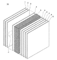
また、後述する液晶表示素子および図1〜4の内容を参考にすると、液晶表示素子に使用される液晶セルの2枚の基板2,8はガラス又はプラスチックの如き柔軟性をもつ透明な材料を用いることができ、一方はシリコン等の不透明な材料でも良い。透明電極(層)6,14を有する透明基板2,8は、例えば、ガラス板2,8等の透明基板上にインジウムスズオキシド(ITO)をスパッタリングすることにより得ることができる。
Further, referring to the liquid crystal display element described later and the contents of FIGS. 1 to 4, the two
前記透明電極(層)やTFTが形成された基板2,8を、透明電極(層)6,14が内側となるように対向させる。その際、スペーサー(図示せず)を介して、基板の間隔を調整してもよい(図1〜4参照)。このときは、得られる調光層の厚さが1〜100μmとなるように調整するのが好ましい。1.5から10μmが更に好ましく、偏光板を使用する場合は、コントラストが最大になるように液晶の屈折率異方性Δnとセル厚dとの積を調整することが好ましい。又、二枚の偏光板1,9がある場合は、各偏光板の偏光軸を調整して視野角やコントラトが良好になるように調整することもできる(図1〜4参照)。更に、視野角を広げるための位相差フィルムも使用することもできる。スペーサーとしては、例えば、ガラス粒子、プラスチック粒子、アルミナ粒子、フォトレジスト材料等が挙げられる。その後、エポキシ系熱硬化性組成物等のシール剤を、液晶注入口を設けた形で該基板にスクリーン印刷し、該基板同士を貼り合わせ、加熱しシール剤を熱硬化させる。
The
上記のように2枚の基板を対向して貼り合わせることにより形成した液晶組成物を収容する液晶組成物収容空間に対して重合性モノマー含有液晶組成物を導入する方法は、通常の真空注入法又はODF法などを用いることができるが、真空注入法においては滴下痕は発生しないものの、注入の後が残る課題を有しているものであるが、本願発明においては、ODF法を用いて製造する表示素子により好適に使用することができる。 The method of introducing the polymerizable monomer-containing liquid crystal composition into the liquid crystal composition containing space containing the liquid crystal composition formed by bonding the two substrates facing each other as described above is a normal vacuum injection method. Alternatively, the ODF method or the like can be used, but although a drop mark is not generated in the vacuum injection method, it has a problem of remaining after the injection, but in the present invention, it is manufactured using the ODF method. The display element can be suitably used.
重合性化合物を重合させる方法としては、液晶の良好な配向性能を得るためには、適度な重合速度が望ましいので、紫外線又は電子線等の活性エネルギー線を単一又は併用又は順番に照射することによって重合させる方法が好ましい。紫外線を使用する場合、偏光光源を用いても良いし、非偏光光源を用いても良い。また、重合性化合物含有液晶組成物を2枚の基板間に挟持させて状態で重合を行う場合には、少なくとも照射面側の基板は活性エネルギー線に対して適当な透明性が与えられていなければならない。また、光照射時にマスクを用いて特定の部分のみを重合させた後、電場や磁場又は温度等の条件を変化させることにより、未重合部分の配向状態を変化させて、更に活性エネルギー線を照射して重合させるという手段を用いても良い。特に紫外線露光する際には、重合性化合物含有液晶組成物に交流電界を印加しながら紫外線露光することが好ましい。印加する交流電界は、周波数10Hzから10kHzの交流が好ましく、周波数60Hzから10kHzがより好ましく、電圧は液晶表示素子の所望のプレチルト角に依存して選ばれる。つまり、印加する電圧により液晶表示素子のプレチルト角を制御することができる。MVAモードの液晶表示素子においては、配向安定性及びコントラストの観点からプレチルト角を80度から89.9度に制御することが好ましい。 As a method for polymerizing a polymerizable compound, an appropriate polymerization rate is desirable in order to obtain good alignment performance of liquid crystals. Therefore, active energy rays such as ultraviolet rays or electron beams are irradiated singly or in combination or sequentially. The method of polymerizing by is preferred. When ultraviolet rays are used, a polarized light source or a non-polarized light source may be used. In addition, when the polymerization is performed in a state where the polymerizable compound-containing liquid crystal composition is sandwiched between two substrates, at least the substrate on the irradiation surface side must be given appropriate transparency to the active energy rays. I must. Moreover, after polymerizing only a specific part using a mask during light irradiation, the orientation state of the unpolymerized part is changed by changing conditions such as an electric field, a magnetic field, or temperature, and further irradiation with active energy rays is performed. Then, it is possible to use a means for polymerization. In particular, when ultraviolet exposure is performed, it is preferable to perform ultraviolet exposure while applying an alternating electric field to the polymerizable compound-containing liquid crystal composition. The alternating electric field to be applied is preferably an alternating current having a frequency of 10 Hz to 10 kHz, more preferably a frequency of 60 Hz to 10 kHz, and the voltage is selected depending on a desired pretilt angle of the liquid crystal display element. That is, the pretilt angle of the liquid crystal display element can be controlled by the applied voltage. In the MVA mode liquid crystal display element, the pretilt angle is preferably controlled from 80 degrees to 89.9 degrees from the viewpoint of alignment stability and contrast.
照射時の温度は、本発明の液晶組成物の液晶状態が保持される温度範囲内であることが好ましい。室温に近い温度、即ち、典型的には15〜35℃での温度で重合させることが好ましい。紫外線を発生させるランプとしては、メタルハライドランプ、高圧水銀ランプ、超高圧水銀ランプ等を用いることができる。また、照射する紫外線の波長としては、液晶組成物の吸収波長域でない波長領域の紫外線を照射することが好ましく、必要に応じて、紫外線をカットして使用することが好ましい。照射する紫外線の強度は、0.1mW/cm2〜100W/cm2が好ましく、2mW/cm2〜50W/cm2がより好ましい。照射する紫外線のエネルギー量は、適宜調整することができるが、10mJ/cm2から500J/cm2が好ましく、100mJ/cm2から200J/cm2がより好ましい。紫外線を照射する際に、強度を変化させても良い。紫外線を照射する時間は照射する紫外線強度により適宜選択されるが、10秒から3600秒が好ましく、10秒から600秒がより好ましい。
The temperature during irradiation is preferably within a temperature range in which the liquid crystal state of the liquid crystal composition of the present invention is maintained. Polymerization is preferably performed at a temperature close to room temperature, that is, typically at a temperature of 15 to 35 ° C. As a lamp for generating ultraviolet rays, a metal halide lamp, a high-pressure mercury lamp, an ultra-high pressure mercury lamp, or the like can be used. Moreover, as a wavelength of the ultraviolet-rays to irradiate, it is preferable to irradiate the ultraviolet-ray of the wavelength range which is not the absorption wavelength range of a liquid crystal composition, and it is preferable to cut and use an ultraviolet-ray as needed. Intensity of ultraviolet irradiation is preferably from 0.1mW / cm 2 ~100W / cm 2 , 2mW /
本発明の第二は、本発明に係る液晶組成物を用いた液晶表示素子である。図1は、液晶表示素子の構成を模式的に示す図である。また、図1では、説明のために便宜上各構成要素を離間して記載している。図2は、当該図1における基板上に形成された薄膜トランジスタを含む電極層3(または薄膜トランジスタ層3とも称する。)のII線で囲まれた領域を拡大した平面図である。図3は、当該図2におけるIII−III線方向に図1に示す液晶表示素子を切断した断面図である。図4は、当該図3におけるIVの領域である薄膜トランジスタを拡大した図である。以下、図1〜4を参照して、本発明に係る液晶表示素子を説明する。 The second aspect of the present invention is a liquid crystal display element using the liquid crystal composition according to the present invention. FIG. 1 is a diagram schematically showing a configuration of a liquid crystal display element. Further, in FIG. 1, for convenience of explanation, each component is illustrated separately. FIG. 2 is an enlarged plan view of a region surrounded by II line of an electrode layer 3 (or also referred to as a thin film transistor layer 3) including a thin film transistor formed on the substrate in FIG. FIG. 3 is a cross-sectional view of the liquid crystal display element shown in FIG. 1 taken along the line III-III in FIG. FIG. 4 is an enlarged view of a thin film transistor which is a region IV in FIG. The liquid crystal display element according to the present invention will be described below with reference to FIGS.
本発明に係る液晶表示素子10の構成は、透明導電性材料からなる透明電極(層)6(または共通電極6とも称する。)を具備した第一の基板8と、透明導電性材料からなる画素電極および各画素に具備した前記画素電極を制御する薄膜トランジスタを形成した薄膜トランジスタ層3を含む第二の基板2と、前記第一の基板8と第二の基板2との間に挟持された液晶組成物(または液晶層5)を有し、該液晶組成物中の液晶分子の電圧無印加時の配向が前記基板2,8に対して略垂直である液晶表示素子であって、該液晶組成物として前記本発明の液晶組成物を用いたことに特徴を有するものである。また図1および図3に示すように、前記第二の基板2および前記第一の基板8は、一対の偏光板1,9間により挟持されてもよい。さらに、図1では、前記第一の基板8と共通電極6との間にカラーフィルタ7が設けられている。またさらに、本発明に係る液晶層5と隣接し、かつ当該液晶層5を構成する液晶組成物と直接当接するよう一対の配向膜4を透明電極(層)6,14表面に形成してもよい。
The configuration of the liquid crystal display element 10 according to the present invention includes a
すなわち、本発明に係る液晶表示素子10は、第二の偏光板1と、第二の基板2と、薄膜トランジスタを含む電極層(又は薄膜トランジスタ層とも称する)3と、配向膜4と、液晶組成物を含む層5と、配向膜4と、共通電極6と、カラーフィルタ7と、第一の基板8と、第一の偏光板9と、が順次積層された構成である。
That is, the liquid crystal display element 10 according to the present invention includes a second
また図2に示すように、第二の基板2の表面に形成されている薄膜トランジスタを含む電極層3は、走査信号を供給するためのゲート配線25と表示信号を供給するためのデータ配線24とが互いに交差しており、かつ前記複数のゲート配線25と複数のデータ配線24とに囲まれた領域には、画素電極21がマトリックス状に形成されている。画素電極21に表示信号を供給するスイッチ素子として、前記ゲート配線25と前記データ配線24が互いに交差している交差部近傍において、ソース電極26、ドレイン電極23およびゲート電極27を含む薄膜トランジスタが、前記画素電極21と連結して設けられている。さらに、前記複数のゲート配線25と複数のデータ配線24とに囲まれた領域にはデータ配線24を介して供給される表示信号を保存するストレイジキャパシタ22が設けられている。
As shown in FIG. 2, the
本発明においては、図2〜4に記載するように薄膜トランジスタが逆スタガード型である液晶表示素子に好適に使用でき、ゲート配線25やデータ配線24などは金属膜であることが好ましく、アルミニウム配線を用いる場合が特に好ましい。さらに、ゲート配線およびデータ配線はゲート絶縁膜を介して重なっている。
In the present invention, as shown in FIGS. 2 to 4, the thin film transistor can be suitably used for a liquid crystal display element having an inverted staggered type, and the
また、当該カラーフィルタ7は、光の漏れを防止する観点で、薄膜トランジスタおよびストレイジキャパシタ22に対応する部分にブラックマトリックス(図示せず)を形成することが好ましい。
The color filter 7 is preferably formed with a black matrix (not shown) in a portion corresponding to the thin film transistor and the
本発明に係る液晶表示素子の薄膜トランジスタの構造の好適な一態様は、例えば、図3および図4で示すように、基板2表面に形成されたゲート電極11と、当該ゲート電極11を覆い、かつ前記基板2の略全面を覆うように設けられたゲート絶縁層13と、前記ゲート電極11と対向するよう前記ゲート絶縁層13の表面に形成された半導体層17と、前記半導体層17の表面の一部を覆うように設けられた保護膜18と、前記保護層18および前記半導体層17の一方の側端部を覆い、かつ前記基板2表面に形成された前記ゲート絶縁層13と接触するように設けられたドレイン電極15と、前記保護膜18および前記半導体層17の他方の側端部を覆い、かつ前記基板2表面に形成された前記ゲート絶縁層13と接触するように設けられたソース電極19a,19bと、前記ソース電極19a,19bを覆い、かつ前記ゲート絶縁層13に倣って前記ゲート絶縁層13の略全面を覆うように設けられた透明電極14と、前記透明電極14の一部および前記ソース電極19a,19bを覆うように設けられた保護層101(図3では図示せず)と、を有している。
A preferred embodiment of the structure of the thin film transistor of the liquid crystal display element according to the present invention includes, for example, a
また、図3および4に示すように、ゲート電極11の表面にゲート電極との段差を無くす等の理由により陽極酸化被膜12を形成してもよい。さらに、ショットキー障壁の幅や高さを低減する目的で半導体層17とドレイン電極15との間にオーミック接触層16を設けても良い。
Further, as shown in FIGS. 3 and 4, an
上述したように液晶表示素子を製造する過程において、滴下痕の発生は、注入される液晶材料に大きな影響を受けるものであるが、液晶表示素子の構成によってもその影響は避けられない。特に、液晶表示素子内に形成されるカラーフィルタ7、又は薄膜トランジスタなどは、図3に示すように、薄い配向膜4や透明電極6,14等だけが液晶組成物と隔てる部材であるため、例えばカラーフィルタに用いられる顔料の化学構造あるいはカラーフィルタ樹脂の化学構造と特定化学構造を有する液晶化合物との組合せにより滴下痕の発生に影響が生じる。
As described above, in the process of manufacturing a liquid crystal display element, the occurrence of dripping marks is greatly affected by the injected liquid crystal material, but the influence is unavoidable depending on the configuration of the liquid crystal display element. In particular, the color filter 7 or the thin film transistor formed in the liquid crystal display element is a member in which only the thin alignment film 4 and the
特に、本発明に係る液晶表示素子の薄膜トランジスタとして上記のような逆スタガード型を使用する場合には、図2〜4に示すようにドレイン電極15がゲート電極11を覆うように形成されるためドレイン電極15の面積が増大する傾向にある。一般にドレイン電極は、銅、アルミニウム、クロム、チタン、モリブデン、タンタル等の金属材料で形成され、パッシベーション処理を施されるのが通常の形態である。しかし、例えば図3および図4で示すように、保護膜18は一般に薄く、配向膜4も薄く、イオン性物質を遮断しない可能性が高いことから、金属材料と液晶組成物の相互作用による滴下痕の発生を避けることができなかった。
In particular, when the above inverted staggered type is used as the thin film transistor of the liquid crystal display device according to the present invention, the
しかし、本発明に係る液晶組成物を含む液晶表示素子では、例えば液晶表示素子の部材と、本発明に係る液晶組成物の表面自由エネルギーあるいは吸着エネルギー等との間の微妙なバランスの観点から滴下痕の発生の問題も低減することができると考えられる。 However, in the liquid crystal display element including the liquid crystal composition according to the present invention, for example, from the viewpoint of a delicate balance between the liquid crystal display element member and the surface free energy or adsorption energy of the liquid crystal composition according to the present invention. It is considered that the problem of generation of marks can be reduced.
本発明の液晶組成物を用いた液晶表示素子は高速応答と表示不良の抑制を両立させた有用なものであり、特に、アクティブマトリックス駆動用液晶表示素子に有用であり、VAモード、PSVAモード、PSAモード、IPSモード又はECBモード用に適用できる。 The liquid crystal display device using the liquid crystal composition of the present invention is useful for achieving both high-speed response and suppression of display failure, and is particularly useful for a liquid crystal display device for active matrix driving, including VA mode, PSVA mode, Applicable for PSA mode, IPS mode or ECB mode.
以下に実施例を挙げて本発明を更に詳述するが、本発明はこれらの実施例に限定されるものではない。また、以下の実施例及び比較例の組成物における「%」は『質量%』を意味する。 EXAMPLES The present invention will be described in further detail with reference to examples below, but the present invention is not limited to these examples. Further, “%” in the compositions of the following Examples and Comparative Examples means “% by mass”.
実施例中、測定した特性は以下の通りである。 In the examples, the measured characteristics are as follows.
Tni :ネマチック相−等方性液体相転移温度(℃)
Δn :25℃における屈折率異方性
Δε :25℃における誘電率異方性
η :20℃における粘度(mPa・s)
γ1 :25℃における回転粘度(mPa・s)
VHR:周波数60Hz,印加電圧1Vの条件下で60℃における電圧保持率(%)
焼き付き :
液晶表示素子の焼き付き評価は、表示エリア内に所定の固定パターンを1000時間表示させた後に、全画面均一な表示を行ったときの固定パターンの残像のレベルを目視にて以下の4段階評価で行った。
T ni : Nematic phase-isotropic liquid phase transition temperature (° C.)
Δn: refractive index anisotropy at 25 ° C. Δε: dielectric anisotropy at 25 ° C. η: viscosity at 20 ° C. (mPa · s)
γ 1 : rotational viscosity at 25 ° C. (mPa · s)
VHR: Voltage holding ratio (%) at 60 ° C. under conditions of frequency 60 Hz and applied voltage 1 V
Burn-in:
The burn-in evaluation of the liquid crystal display element is based on the following four-level evaluation of the afterimage level of the fixed pattern when the predetermined fixed pattern is displayed in the display area for 1000 hours and then the entire screen is uniformly displayed. went.
◎残像無し
○残像ごく僅かに有るも許容できるレベル
△残像有り許容できないレベル
×残像有りかなり劣悪
滴下痕 :
液晶表示装置の滴下痕の評価は、全面黒表示した場合における白く浮かび上がる滴下痕を目視にて以下の4段階評価で行った。
◎ No afterimage ○ Very little afterimage but acceptable level △ There is afterimage unacceptable level × Afterimage is quite bad Drop mark:
Evaluation of the drop marks of the liquid crystal display device was performed by the following four-stage evaluation of the drop marks that appeared white when the entire surface was displayed in black.
◎残像無し
○残像ごく僅かに有るも許容できるレベル
△残像有り許容できないレベル
×残像有りかなり劣悪
プロセス適合性 :
プロセス適合性は、ODFプロセスにおいて、定積計量ポンプを用いて1回に50pLずつ液晶を滴下することを100000回行い、次の「0〜100回、101〜200回、201〜300回、・・・・99901〜100000回」の各100回ずつ滴下された液晶量の変化を以下の4段階で評価した。
◎ No afterimage ○ Very little afterimage but acceptable level △ With afterimage unacceptable level × With afterimage Quite poor process suitability:
The process suitability is that the liquid crystal is dropped by 50 pL at a time using a constant volume metering pump 100000 times in the ODF process, and the following “0 to 100 times, 101 to 200 times, 201 to 300 times, ... 99901 to 100,000 times ”was evaluated for changes in the amount of liquid crystal dropped 100 times each in the following four stages.
◎変化が極めて小さい(安定的に液晶表示素子を製造できる)
○変化が僅かに有るも許容できるレベル
△変化が有り許容できないレベル(斑発生により歩留まりが悪化)
×変化が有りかなり劣悪(液晶漏れや真空気泡が発生)
低温での溶解性:
低温での溶解性評価は、液晶組成物を調製後、2mLのサンプル瓶に液晶組成物を1g秤量し、これに温度制御式試験槽の中で、次を1サイクル「−20℃(1時間保持)→昇温(0.1℃/毎分)→0℃(1時間保持)→昇温(0.1℃/毎分)→20℃(1時間保持)→降温(−0.1℃/毎分)→0℃(1時間保持)→降温(−0.1℃/毎分)→−20℃」として温度変化を与え続け、目視にて液晶組成物からの析出物の発生を観察し、以下の4段階評価を行った。
◎ Extremely small change (Stable liquid crystal display device can be manufactured)
○ Allowable level with slight change △ Level with change and unacceptable level (Yield deteriorated due to spots)
× There is a change and it is quite inferior (liquid crystal leakage and vacuum bubbles are generated)
Solubility at low temperature:
In order to evaluate the solubility at a low temperature, after preparing the liquid crystal composition, 1 g of the liquid crystal composition was weighed into a 2 mL sample bottle, and the next was “−20 ° C. (1 hour) in a temperature-controlled test tank. Hold) → Temperature rise (0.1 ° C./min)→0° C. (hold for 1 hour) → Temperature rise (0.1 ° C./min)→20° C. (hold for 1 hour) → Temperature drop (−0.1 ° C.) / Min) → 0 ° C. (hold for 1 hour) → temperature drop (−0.1 ° C./min)→−20° C. ”, and visually observe the occurrence of precipitates from the liquid crystal composition Then, the following four-stage evaluation was performed.
◎600時間以上析出物が観察されなかった。 A precipitate was not observed for 600 hours or more.
○300時間以上析出物が観察されなかった。 ○ No precipitate was observed for 300 hours or more.
△150時間以内に析出物が観察された。 Precipitates were observed within Δ150 hours.
×75時間以内に析出物が観察された。
尚、実施例において化合物の記載について以下の略号を用いる。
(側鎖)
−n −CnH2n+1 炭素原子数nの直鎖状アルキル基
−On −OCnH2n+1 炭素原子数nの直鎖状アルコキシ基
−V −C=CH2 ビニル基
−Vn −C=C−CnH2n+1 炭素原子数(n+1)の1−アルケン
(環構造)
X Precipitates were observed within 75 hours.
In the examples, the following abbreviations are used for the description of compounds.
(Side chain)
-N -C n H 2n + 1 linear alkyl group with n carbon atoms -On -OC n H 2n + 1 linear alkoxy group with n carbon atoms -V -C = CH 2 vinyl group -Vn -C = C- C n H 2n + 1 carbon atom number (n + 1) 1-alkene (ring structure)
(実施例1)
次に示す組成を有する液晶組成物(実施例1)を調製し、その物性値を測定した。この結果を次の表に示す。
(Example 1)
A liquid crystal composition (Example 1) having the following composition was prepared and measured for physical properties. The results are shown in the following table.
実施例1の液晶組成物を用いて、VA液晶表示素子を作製した。この液晶表示素子は、アクティブ素子として逆スタガード型の薄膜トランジスタを有している。液晶組成物の注入は、滴下法にて行い、焼き付き、滴下痕、プロセス適合性及び低温での溶解性の評価を行った。 A VA liquid crystal display device was produced using the liquid crystal composition of Example 1. This liquid crystal display element has an inverted staggered thin film transistor as an active element. The liquid crystal composition was injected by a dropping method, and image sticking, dropping marks, process suitability, and solubility at low temperatures were evaluated.
尚、含有量の左側の記号は、上記化合物の略号の記載である。 The symbol on the left side of the content is a description of the abbreviation for the above compound.
実施例1の液晶組成物は、TV用液晶組成物として実用的な75.3℃の液晶相温度範囲を有し、大きい誘電率異方性の絶対値を有し、低い粘性及び最適なΔnを有していることが解る。実施例1記載の液晶組成物を用いて、VA液晶表示素子を作製し前述の方法により、焼き付き、滴下痕、プロセス適合性及び低温での溶解性を評価したところ、極めて優れた評価結果を示した。
(比較例1)
一般式(II)で表される化合物を含有せず、実施例1の組成物と同等の液晶相温度範囲、同等の屈折率異方性の値及び同等の誘電率異方性の値を有するように設計した以下に示される液晶組成物(比較例1)を調製し、その物性値を測定した。この結果を次の表に示す。
The liquid crystal composition of Example 1 has a liquid crystal phase temperature range of 75.3 ° C. that is practical as a liquid crystal composition for TV, has a large absolute value of dielectric anisotropy, low viscosity, and an optimal Δn. It can be seen that Using the liquid crystal composition described in Example 1, a VA liquid crystal display element was prepared and evaluated for burn-in, dripping marks, process suitability, and solubility at low temperatures by the method described above. It was.
(Comparative Example 1)
Does not contain the compound represented by the general formula (II), has a liquid crystal phase temperature range equivalent to the composition of Example 1, an equivalent value of refractive index anisotropy, and an equivalent value of dielectric anisotropy. The liquid crystal composition shown below (Comparative Example 1) designed as described above was prepared, and its physical properties were measured. The results are shown in the following table.
比較例1の液晶組成物を用いて、実施例1と同様にVA液晶表示素子を作製し、焼き付き、滴下痕、プロセス適合性及び低温での溶解性の評価を行った結果を同じ表に示す。 Using the liquid crystal composition of Comparative Example 1, a VA liquid crystal display device was produced in the same manner as in Example 1, and the results of evaluation of image sticking, dripping marks, process compatibility, and solubility at low temperatures are shown in the same table. .
尚、含有量の左側の記号は、実施例1と同様に、前記化合物略号の記載である。 In addition, the symbol on the left side of the content is the description of the compound abbreviation as in Example 1.
一般式(II)で表される化合物を含有しない液晶組成物(比較例1)は、一般式(II)で表される化合物を11%質量含有する液晶組成物(実施例1)と比べて、同等の液晶相温度範囲、同等の屈折率異方性の値及び同等の誘電率異方性の値を有するものの、粘度ηが上昇することが示された。γ1については、比較例1の値である111mPa・sは実施例1の値である106mPa・sと比較して高い値を示しており、液晶表示素子及びディスプレイにおける実効的な応答速度を表すパラメータであるγ1/Δn2の値で比較しても劣る結果となった。比較例1の初期のVHRは99.3%であったのに対し、150℃で1時間の高温放置後のVHRは、98.5%であり、実施例1と比較して劣る結果となった。プロセス適合性について評価したところ、実施例1と比べて変化が許容できないレベルとなった。低温での溶解性を評価したところ、実施例1と比べて早期に析出が観察された。
(比較例2)
一般式(I)で表される化合物を含有せず、実施例1の組成物と同等の液晶相温度範囲、同等の屈折率異方性の値及び同等の誘電率異方性の値を有するように設計した以下に示される液晶組成物(比較例2)を調製し、その物性値を測定した。この結果を次の表に示す。
The liquid crystal composition not containing the compound represented by the general formula (II) (Comparative Example 1) is compared with the liquid crystal composition containing 11% by mass of the compound represented by the general formula (II) (Example 1). Although the liquid crystal phase temperature range, the value of the refractive index anisotropy and the value of the dielectric anisotropy were the same, it was shown that the viscosity η increased. As for γ1, 111 mPa · s, which is the value of Comparative Example 1, is higher than 106 mPa · s, which is the value of Example 1, and is a parameter representing an effective response speed in the liquid crystal display element and the display. It resulted inferior compared with the value of .gamma.1 / [Delta] n 2 is. The initial VHR of Comparative Example 1 was 99.3%, whereas the VHR after standing at high temperature for 1 hour at 150 ° C. was 98.5%, which is inferior to that of Example 1. It was. When the process suitability was evaluated, the change was unacceptable as compared with Example 1. When the solubility at a low temperature was evaluated, precipitation was observed earlier than in Example 1.
(Comparative Example 2)
Does not contain the compound represented by the general formula (I), has a liquid crystal phase temperature range equivalent to the composition of Example 1, an equivalent value of refractive index anisotropy, and an equivalent value of dielectric anisotropy The liquid crystal composition shown below (Comparative Example 2) designed as described above was prepared, and its physical property values were measured. The results are shown in the following table.
比較例2の液晶組成物を用いて、実施例1と同様にVA液晶表示素子を作製し、焼き付き、滴下痕、プロセス適合性及び低温での溶解性の評価を行った結果を同じ表に示す。 Using the liquid crystal composition of Comparative Example 2, a VA liquid crystal display device was prepared in the same manner as in Example 1, and the results of evaluation of image sticking, dripping marks, process suitability, and solubility at low temperatures are shown in the same table. .
一般式(I)で表される化合物を含有しない液晶組成物(比較例2)は、一般式(I)で表される化合物を28%質量含有する液晶組成物(実施例1)と比べて、同等の液晶相温度範囲、同等の屈折率異方性の値及び同等の誘電率異方性の値を有するものの、粘度ηが上昇することが示された。γ1については、比較例2の値である132mPa・sは実施例1の値である106mPa・sと比較して高い値を示しており、液晶表示素子及びディスプレイにおける実効的な応答速度を表すパラメータであるγ1/Δn2の値で比較しても劣る結果となった。比較例2の初期のVHRは99.3%であったのに対し、150℃で1時間の高温放置後のVHRは、98.6%であり、実施例1と比較して劣る結果となった。プロセス適合性について評価したところ、実施例1と比べて変化が許容できないレベルとなった。低温での溶解性を評価したところ、実施例1と比べて早期に析出が観察された。
(実施例2)
実施例1の組成物と同等の液晶相温度範囲、同等の屈折率異方性の値及び同等の誘電率異方性の値を有するように設計した次に示す組成を有する液晶組成物(実施例2)を調製し、その物性値を測定した。この結果を次の表に示す。
The liquid crystal composition not containing the compound represented by the general formula (I) (Comparative Example 2) is compared with the liquid crystal composition containing 28% by mass of the compound represented by the general formula (I) (Example 1). Although the liquid crystal phase temperature range, the value of the refractive index anisotropy and the value of the dielectric anisotropy were the same, it was shown that the viscosity η increased. As for γ1, 132 mPa · s, which is the value of Comparative Example 2, is higher than 106 mPa · s, which is the value of Example 1, and is a parameter representing an effective response speed in the liquid crystal display element and the display. It resulted inferior compared with the value of .gamma.1 / [Delta] n 2 is. The initial VHR of Comparative Example 2 was 99.3%, whereas the VHR after standing at high temperature for 1 hour at 150 ° C. was 98.6%, which was inferior to that of Example 1. It was. When the process suitability was evaluated, the change was unacceptable as compared with Example 1. When the solubility at a low temperature was evaluated, precipitation was observed earlier than in Example 1.
(Example 2)
A liquid crystal composition having the following composition designed to have a liquid crystal phase temperature range equivalent to the composition of Example 1, an equivalent value of refractive index anisotropy, and an equivalent value of dielectric anisotropy (implementation) Example 2) was prepared and its physical properties were measured. The results are shown in the following table.
実施例2の液晶組成物を用いて、実施例1と同様にVA液晶表示素子を作製し、焼き付き、滴下痕、プロセス適合性及び低温での溶解性の評価を行った結果を同じ表に示す。 Using the liquid crystal composition of Example 2, a VA liquid crystal display device was prepared in the same manner as in Example 1, and the results of evaluation of image sticking, dripping marks, process suitability, and solubility at low temperatures are shown in the same table. .
実施例2の液晶組成物は、TV用液晶組成物として実用的な液晶相温度範囲を有し、大きい誘電率異方性の絶対値を有し、低い粘性及び最適なΔnを有していることが解る。実施例2記載の液晶組成物を用いて、VA液晶表示素子を作製し前述の方法により、焼き付き、滴下痕、プロセス適合性及び低温での溶解性を評価したところ、優れた評価結果を示した。
(比較例3)
一般式(II)で表される化合物を含有せず、実施例2の組成物と同等の液晶相温度範囲、同等の屈折率異方性の値及び同等の誘電率異方性の値を有するように設計した以下に示される液晶組成物(比較例3)を調製し、その物性値を測定した。この結果を次の表に示す。
The liquid crystal composition of Example 2 has a practical liquid crystal phase temperature range as a liquid crystal composition for TV, has a large absolute value of dielectric anisotropy, has a low viscosity, and an optimal Δn. I understand that. Using the liquid crystal composition described in Example 2, a VA liquid crystal display device was prepared and evaluated for burn-in, dripping marks, process suitability, and solubility at low temperatures by the above-described methods, and an excellent evaluation result was shown. .
(Comparative Example 3)
Does not contain the compound represented by the general formula (II), and has the same liquid crystal phase temperature range, equivalent refractive index anisotropy value and equivalent dielectric anisotropy value as the composition of Example 2. A liquid crystal composition shown below (Comparative Example 3) designed as described above was prepared, and its physical property values were measured. The results are shown in the following table.
比較例3の液晶組成物を用いて、実施例2と同様にVA液晶表示素子を作製し、焼き付き、滴下痕、プロセス適合性及び低温での溶解性の評価を行った結果を同じ表に示す。 Using the liquid crystal composition of Comparative Example 3, a VA liquid crystal display device was prepared in the same manner as in Example 2, and the results of evaluation of image sticking, dripping marks, process compatibility, and solubility at low temperatures are shown in the same table. .
一般式(II)で表される化合物を含有しない液晶組成物(比較例3)は、一般式(I)で表される化合物を11%質量含有する液晶組成物(実施例2)と比べて、同等の液晶相温度範囲、同等の屈折率異方性の値及び同等の誘電率異方性の値を有するものの、粘度ηが上昇することが示された。γ1については、比較例3の値である114mPa・sは実施例2の値である105mPa・sと比較して高い値を示しており、液晶表示素子及びディスプレイにおける実効的な応答速度を表すパラメータであるγ1/Δn2の値で比較しても劣る結果となった。比較例3の初期のVHRは99.4%であったのに対し、150℃で1時間の高温放置後のVHRは、98.7%であり、実施例2と比較して劣る結果となった。プロセス適合性について評価したところ、実施例2と比べて変化が許容できないレベルとなった。低温での溶解性を評価したところ、実施例2と比べて早期に析出が観察された。
(実施例3及び実施例4)
実施例1の組成物と同等の液晶相温度範囲、同等の屈折率異方性の値及び同等の誘電率異方性の値を有するように設計した次に示す組成を有する液晶組成物(実施例3及び実施例4)を調製し、その物性値を測定した。この結果を次の表に示す。
The liquid crystal composition not containing the compound represented by the general formula (II) (Comparative Example 3) is compared with the liquid crystal composition containing 11% by mass of the compound represented by the general formula (I) (Example 2). Although the liquid crystal phase temperature range, the value of the refractive index anisotropy and the value of the dielectric anisotropy were the same, it was shown that the viscosity η increased. As for γ1, 114 mPa · s, which is the value of Comparative Example 3, is higher than 105 mPa · s, which is the value of Example 2, and is a parameter representing an effective response speed in the liquid crystal display element and the display. It resulted inferior compared with the value of .gamma.1 / [Delta] n 2 is. While the initial VHR of Comparative Example 3 was 99.4%, the VHR after high temperature standing at 150 ° C. for 1 hour was 98.7%, which is inferior to that of Example 2. It was. When the process suitability was evaluated, the change was unacceptable as compared with Example 2. When the solubility at low temperature was evaluated, precipitation was observed earlier than in Example 2.
(Example 3 and Example 4)
A liquid crystal composition having the following composition designed to have a liquid crystal phase temperature range equivalent to the composition of Example 1, an equivalent value of refractive index anisotropy, and an equivalent value of dielectric anisotropy (implementation) Example 3 and Example 4) were prepared and their physical properties were measured. The results are shown in the following table.
実施例3及び実施例4の液晶組成物を用いて、実施例1と同様にVA液晶表示素子を作製し、焼き付き、滴下痕、プロセス適合性及び低温での溶解性の評価を行った結果を同じ表に示す。 Using the liquid crystal compositions of Example 3 and Example 4, a VA liquid crystal display device was produced in the same manner as in Example 1, and the results of evaluation of image sticking, dripping marks, process suitability, and solubility at low temperatures were obtained. Shown in the same table.
実施例3の液晶組成物は、TV用液晶組成物として実用的な液晶相温度範囲を有し、大きい誘電率異方性の絶対値を有し、低い粘性及び最適なΔnを有していることが解る。実施例3記載の液晶組成物を用いて、VA液晶表示素子を作製し前述の方法により、焼き付き、滴下痕、プロセス適合性及び低温での溶解性を評価したところ、優れた評価結果を示した。 The liquid crystal composition of Example 3 has a practical liquid crystal phase temperature range as a liquid crystal composition for TV, a large absolute value of dielectric anisotropy, a low viscosity, and an optimal Δn. I understand that. Using the liquid crystal composition described in Example 3, a VA liquid crystal display device was prepared and evaluated for burn-in, dripping marks, process suitability, and solubility at low temperatures by the above-described methods, and excellent evaluation results were shown. .
実施例4の液晶組成物は、TV用液晶組成物として実用的な液晶相温度範囲を有し、大きい誘電率異方性の絶対値を有し、低い粘性及び最適なΔnを有していることが解る。実施例4記載の液晶組成物を用いて、VA液晶表示素子を作製し前述の方法により、焼き付き、滴下痕、プロセス適合性及び低温での溶解性を評価したところ、優れた評価結果を示した。
(実施例5及び実施例6)
実施例1の組成物と同等の液晶相温度範囲、同等の屈折率異方性の値及び同等の誘電率異方性の値を有するように設計した次に示す組成を有する液晶組成物(実施例5及び実施例6)を調製し、その物性値を測定した。この結果を次の表に示す。
The liquid crystal composition of Example 4 has a practical liquid crystal phase temperature range as a liquid crystal composition for TV, has a large absolute value of dielectric anisotropy, has a low viscosity, and an optimal Δn. I understand that. Using the liquid crystal composition described in Example 4, a VA liquid crystal display device was prepared and evaluated for burn-in, dripping marks, process suitability, and solubility at low temperatures by the above-described methods, and an excellent evaluation result was shown. .
(Example 5 and Example 6)
A liquid crystal composition having the following composition designed to have a liquid crystal phase temperature range equivalent to the composition of Example 1, an equivalent value of refractive index anisotropy, and an equivalent value of dielectric anisotropy (implementation) Example 5 and Example 6) were prepared and their physical properties were measured. The results are shown in the following table.
実施例5及び実施例6の液晶組成物を用いて、実施例1と同様にVA液晶表示素子を作製し、焼き付き、滴下痕、プロセス適合性及び低温での溶解性の評価を行った結果を同じ表に示す。 Using the liquid crystal compositions of Example 5 and Example 6, a VA liquid crystal display element was produced in the same manner as in Example 1, and the results of evaluation of image sticking, dripping marks, process suitability, and solubility at low temperatures were obtained. Shown in the same table.
実施例5の液晶組成物は、TV用液晶組成物として実用的な液晶相温度範囲を有し、大きい誘電率異方性の絶対値を有し、低い粘性及び最適なΔnを有していることが解る。実施例5記載の液晶組成物を用いて、VA液晶表示素子を作製し前述の方法により、焼き付き、滴下痕、プロセス適合性及び低温での溶解性を評価したところ、優れた評価結果を示した。 The liquid crystal composition of Example 5 has a practical liquid crystal phase temperature range as a liquid crystal composition for TV, has a large absolute value of dielectric anisotropy, has a low viscosity, and an optimal Δn. I understand that. Using the liquid crystal composition described in Example 5, a VA liquid crystal display element was prepared and evaluated for image sticking, dripping marks, process suitability, and solubility at low temperatures by the above-described method, and showed excellent evaluation results. .
実施例6の液晶組成物は、TV用液晶組成物として実用的な液晶相温度範囲を有し、大きい誘電率異方性の絶対値を有し、低い粘性及び最適なΔnを有していることが解る。実施例6記載の液晶組成物を用いて、VA液晶表示素子を作製し前述の方法により、焼き付き、滴下痕、プロセス適合性及び低温での溶解性を評価したところ、優れた評価結果を示した。
(実施例7)
実施例1の組成物と同等の液晶相温度範囲、同等の屈折率異方性の値及び同等の誘電率異方性の値を有するように設計した次に示す組成を有する液晶組成物(実施例7)を調製し、その物性値を測定した。この結果を次の表に示す。
The liquid crystal composition of Example 6 has a practical liquid crystal phase temperature range as a liquid crystal composition for TV, has a large absolute value of dielectric anisotropy, has a low viscosity, and an optimal Δn. I understand that. Using the liquid crystal composition described in Example 6, a VA liquid crystal display element was prepared, and when the image sticking, dripping marks, process suitability, and solubility at low temperature were evaluated by the above-described method, excellent evaluation results were shown. .
(Example 7)
A liquid crystal composition having the following composition designed to have a liquid crystal phase temperature range equivalent to the composition of Example 1, an equivalent value of refractive index anisotropy, and an equivalent value of dielectric anisotropy (implementation) Example 7) was prepared and its physical properties were measured. The results are shown in the following table.
実施例7の液晶組成物を用いて、実施例1と同様にVA液晶表示素子を作製し、焼き付き、滴下痕、プロセス適合性及び低温での溶解性の評価を行った結果を同じ表に示す。 Using the liquid crystal composition of Example 7, a VA liquid crystal display device was prepared in the same manner as in Example 1, and the results of evaluation of image sticking, dripping marks, process suitability, and solubility at low temperatures are shown in the same table. .
実施例7の液晶組成物は、TV用液晶組成物として実用的な液晶相温度範囲を有し、大きい誘電率異方性の絶対値を有し、低い粘性及び最適なΔnを有していることが解る。実施例7記載の液晶組成物を用いて、VA液晶表示素子を作製し前述の方法により、焼き付き、滴下痕、プロセス適合性及び低温での溶解性を評価したところ、優れた評価結果を示した。
(比較例4)
一般式(I)で表される化合物を含有せず、実施例7の組成物と同等の液晶相温度範囲、同等の屈折率異方性の値及び同等の誘電率異方性の値を有するように設計した以下に示される液晶組成物(比較例4)を調製し、その物性値を測定した。この結果を次の表に示す。
The liquid crystal composition of Example 7 has a practical liquid crystal phase temperature range as a liquid crystal composition for TV, has a large absolute value of dielectric anisotropy, has a low viscosity, and an optimal Δn. I understand that. Using the liquid crystal composition described in Example 7, a VA liquid crystal display device was prepared and evaluated for burn-in, dripping marks, process suitability, and solubility at low temperatures by the above-described methods, and an excellent evaluation result was shown. .
(Comparative Example 4)
Does not contain the compound represented by the general formula (I), has the same liquid crystal phase temperature range, equivalent refractive index anisotropy value and equivalent dielectric anisotropy value as the composition of Example 7. The liquid crystal composition shown below (Comparative Example 4) designed as described above was prepared, and its physical properties were measured. The results are shown in the following table.
比較例4の液晶組成物を用いて、実施例7と同様にVA液晶表示素子を作製し、焼き付き、滴下痕、プロセス適合性及び低温での溶解性の評価を行った結果を同じ表に示す。 Using the liquid crystal composition of Comparative Example 4, a VA liquid crystal display device was produced in the same manner as in Example 7, and the results of evaluation of image sticking, dripping marks, process suitability, and solubility at low temperatures are shown in the same table. .
一般式(I)で表される化合物を含有しない液晶組成物(比較例4)は、一般式(I)で表される化合物を29%質量含有する液晶組成物(実施例7)と比べて、同等の液晶相温度範囲、同等の屈折率異方性の値及び同等の誘電率異方性の値を有するものの、粘度ηが上昇することが示された。γ1については、比較例4の値である132mPa・sは実施例7の値である108mPa・sと比較して高い値を示しており、液晶表示素子及びディスプレイにおける実効的な応答速度を表すパラメータであるγ1/Δn2の値で比較しても劣る結果となった。比較例4の初期のVHRは99.3%であったのに対し、150℃で1時間の高温放置後のVHRは、98.6%であり、実施例7と比較して劣る結果となった。プロセス適合性について評価したところ、実施例7と比べて変化が許容できないレベルとなった。低温での溶解性を評価したところ、実施例7と比べて早期に析出が観察された。
(実施例8及び実施例9)
実施例7の組成物と同等の液晶相温度範囲、同等の屈折率異方性の値及び同等の誘電率異方性の値を有するように設計した次に示す組成を有する液晶組成物(実施例8及び実施例9)を調製し、その物性値を測定した。この結果を次の表に示す。
The liquid crystal composition not containing the compound represented by the general formula (I) (Comparative Example 4) is compared with the liquid crystal composition containing 29% by mass of the compound represented by the general formula (I) (Example 7). Although the liquid crystal phase temperature range, the value of the refractive index anisotropy and the value of the dielectric anisotropy were the same, it was shown that the viscosity η increased. For γ1, 132 mPa · s, which is the value in Comparative Example 4, is higher than 108 mPa · s, which is the value in Example 7, and is a parameter representing an effective response speed in the liquid crystal display element and the display. It resulted inferior compared with the value of .gamma.1 / [Delta] n 2 is. While the initial VHR of Comparative Example 4 was 99.3%, the VHR after high temperature standing at 150 ° C. for 1 hour was 98.6%, which is inferior to Example 7. It was. When the process suitability was evaluated, the change was unacceptable as compared with Example 7. When the solubility at low temperature was evaluated, precipitation was observed earlier than in Example 7.
(Example 8 and Example 9)
A liquid crystal composition having the following composition designed to have a liquid crystal phase temperature range equivalent to the composition of Example 7, an equivalent value of refractive index anisotropy, and an equivalent value of dielectric anisotropy (implementation) Example 8 and Example 9) were prepared and their physical properties were measured. The results are shown in the following table.
実施例8及び実施例9の液晶組成物を用いて、実施例1と同様にVA液晶表示素子を作製し、焼き付き、滴下痕、プロセス適合性及び低温での溶解性の評価を行った結果を同じ表に示す。 Using the liquid crystal compositions of Example 8 and Example 9, a VA liquid crystal display device was produced in the same manner as in Example 1, and the results of evaluation of image sticking, dripping marks, process suitability, and solubility at low temperatures were obtained. Shown in the same table.
実施例8の液晶組成物は、TV用液晶組成物として実用的な液晶相温度範囲を有し、大きい誘電率異方性の絶対値を有し、低い粘性及び最適なΔnを有していることが解る。実施例8記載の液晶組成物を用いて、VA液晶表示素子を作製し前述の方法により、焼き付き、滴下痕、プロセス適合性及び低温での溶解性を評価したところ、優れた評価結果を示した。 The liquid crystal composition of Example 8 has a practical liquid crystal phase temperature range as a liquid crystal composition for TV, has a large absolute value of dielectric anisotropy, has a low viscosity, and an optimal Δn. I understand that. Using the liquid crystal composition described in Example 8, a VA liquid crystal display device was prepared and evaluated for burn-in, dripping marks, process suitability, and solubility at low temperatures by the above-described methods, and an excellent evaluation result was shown. .
実施例9の液晶組成物は、TV用液晶組成物として実用的な液晶相温度範囲を有し、大きい誘電率異方性の絶対値を有し、低い粘性及び最適なΔnを有していることが解る。実施例9記載の液晶組成物を用いて、VA液晶表示素子を作製し前述の方法により、焼き付き、滴下痕、プロセス適合性及び低温での溶解性を評価したところ、優れた評価結果を示した。
(実施例10及び実施例11)
実施例7の組成物と同等の液晶相温度範囲、同等の屈折率異方性の値及び同等の誘電率異方性の値を有するように設計した次に示す組成を有する液晶組成物(実施例10及び実施例11)を調製し、その物性値を測定した。この結果を次の表に示す。
The liquid crystal composition of Example 9 has a practical liquid crystal phase temperature range as a liquid crystal composition for TV, a large absolute value of dielectric anisotropy, a low viscosity, and an optimal Δn. I understand that. Using the liquid crystal composition described in Example 9, a VA liquid crystal display device was prepared and evaluated for burn-in, dripping marks, process suitability, and solubility at low temperatures by the above-mentioned methods, and an excellent evaluation result was shown. .
(Example 10 and Example 11)
A liquid crystal composition having the following composition designed to have a liquid crystal phase temperature range equivalent to the composition of Example 7, an equivalent value of refractive index anisotropy, and an equivalent value of dielectric anisotropy (implementation) Example 10 and Example 11) were prepared and their physical properties were measured. The results are shown in the following table.
実施例10及び実施例11の液晶組成物を用いて、実施例1と同様にVA液晶表示素子を作製し、焼き付き、滴下痕、プロセス適合性及び低温での溶解性の評価を行った結果を同じ表に示す。 Using the liquid crystal compositions of Example 10 and Example 11, a VA liquid crystal display element was produced in the same manner as in Example 1, and the results of evaluation of image sticking, dripping marks, process suitability, and solubility at low temperatures were obtained. Shown in the same table.
実施例10の液晶組成物は、TV用液晶組成物として実用的な液晶相温度範囲を有し、大きい誘電率異方性の絶対値を有し、低い粘性及び最適なΔnを有していることが解る。実施例10記載の液晶組成物を用いて、VA液晶表示素子を作製し前述の方法により、焼き付き、滴下痕、プロセス適合性及び低温での溶解性を評価したところ、優れた評価結果を示した。 The liquid crystal composition of Example 10 has a practical liquid crystal phase temperature range as a liquid crystal composition for TV, has a large absolute value of dielectric anisotropy, has a low viscosity, and an optimal Δn. I understand that. Using the liquid crystal composition described in Example 10, a VA liquid crystal display element was prepared, and the image sticking, dripping marks, process suitability, and solubility at low temperatures were evaluated by the above-described method. .
実施例11の液晶組成物は、TV用液晶組成物として実用的な液晶相温度範囲を有し、大きい誘電率異方性の絶対値を有し、低い粘性及び最適なΔnを有していることが解る。実施例11記載の液晶組成物を用いて、VA液晶表示素子を作製し前述の方法により、焼き付き、滴下痕、プロセス適合性及び低温での溶解性を評価したところ、優れた評価結果を示した。
(実施例12)
実施例7の組成物と同等の液晶相温度範囲、同等の屈折率異方性の値及び同等の誘電率異方性の値を有するように設計した次に示す組成を有する液晶組成物(実施例12)を調製し、その物性値を測定した。この結果を次の表に示す。
The liquid crystal composition of Example 11 has a practical liquid crystal phase temperature range as a liquid crystal composition for TV, has a large absolute value of dielectric anisotropy, has a low viscosity, and an optimal Δn. I understand that. Using the liquid crystal composition described in Example 11, a VA liquid crystal display device was prepared and evaluated for burn-in, dripping marks, process suitability, and solubility at low temperatures by the above-described methods, and an excellent evaluation result was shown. .
(Example 12)
A liquid crystal composition having the following composition designed to have a liquid crystal phase temperature range equivalent to the composition of Example 7, an equivalent value of refractive index anisotropy, and an equivalent value of dielectric anisotropy (implementation) Example 12) was prepared and its physical properties were measured. The results are shown in the following table.
実施例12及び実施例11の液晶組成物を用いて、実施例1と同様にVA液晶表示素子を作製し、焼き付き、滴下痕、プロセス適合性及び低温での溶解性の評価を行った結果を同じ表に示す。 Using the liquid crystal compositions of Example 12 and Example 11, a VA liquid crystal display element was prepared in the same manner as in Example 1, and the results of evaluation of image sticking, dripping marks, process suitability, and solubility at low temperatures were obtained. Shown in the same table.
実施例12の液晶組成物は、TV用液晶組成物として実用的な液晶相温度範囲を有し、大きい誘電率異方性の絶対値を有し、低い粘性及び最適なΔnを有していることが解る。実施例12記載の液晶組成物を用いて、VA液晶表示素子を作製し前述の方法により、焼き付き、滴下痕、プロセス適合性及び低温での溶解性を評価したところ、優れた評価結果を示した。 The liquid crystal composition of Example 12 has a practical liquid crystal phase temperature range as a liquid crystal composition for TV, has a large absolute value of dielectric anisotropy, has a low viscosity, and an optimal Δn. I understand that. Using the liquid crystal composition described in Example 12, a VA liquid crystal display device was prepared and evaluated for burn-in, dripping marks, process suitability, and solubility at low temperatures by the above-described method, and an excellent evaluation result was shown. .
(符号の説明)
1 第二の偏光板
2 第二の基板
3 薄膜トランジスタ層または薄膜トランジスタを含む電極層
4 配向膜
5 液晶層
6 画素電極(共通電極)
7 カラーフィルター
8 第一の基板
9 第一の偏光板
10 液晶表示素子
11 ゲート電極
12 陽極酸化被膜
13 ゲート絶縁層
14 透明電極(層)
15 ドレイン電極
16 オーミック接触層
17 半導体層
18 保護膜
19a,19b ソース電極
21 画素電極
22 ストレイジキャパシタ
23 ドレイン電極
24 データ配線
25 ゲート配線
26 ソース電極
27 ゲート電極
101 保護層
(Explanation of symbols)
DESCRIPTION OF
7
DESCRIPTION OF
Claims (9)
A3は1,4−シクロヘキシレン基、1,4−フェニレン基又はテトラヒドロピラン−2,5−ジイル基を表すが、A3が1,4−フェニレン基を表す場合、該1,4−フェニレン基中の1つ以上の水素原子はフッ素原子に置換されていてもよく、
Z1は単結合、−OCH2−、−OCF2−、−CH2O−、又は−CF2O−を表し、
nは0又は1を表し、
X1〜X6はそれぞれ独立して水素原子、又はフッ素原子を表すが、X1〜X6の少なくとも1つはフッ素原子を表す。)で表される化合物群より選ばれる化合物を1種又は2種以上含有する請求項1に記載の液晶組成物。 Furthermore, the general formula (V)
A 3 represents a 1,4-cyclohexylene group, a 1,4-phenylene group or a tetrahydropyran-2,5-diyl group, and when A 3 represents a 1,4-phenylene group, One or more hydrogen atoms in the group may be substituted with fluorine atoms,
Z 1 represents a single bond, —OCH 2 —, —OCF 2 —, —CH 2 O—, or —CF 2 O—,
n represents 0 or 1,
X 1 to X 6 each independently represent a hydrogen atom or a fluorine atom, but at least one of X 1 to X 6 represents a fluorine atom. The liquid crystal composition according to claim 1, comprising one or more compounds selected from the group of compounds represented by:
Priority Applications (1)
| Application Number | Priority Date | Filing Date | Title |
|---|---|---|---|
| JP2015086772A JP2015199961A (en) | 2015-04-21 | 2015-04-21 | Liquid crystal composition and liquid crystal display element using the same |
Applications Claiming Priority (1)
| Application Number | Priority Date | Filing Date | Title |
|---|---|---|---|
| JP2015086772A JP2015199961A (en) | 2015-04-21 | 2015-04-21 | Liquid crystal composition and liquid crystal display element using the same |
Related Parent Applications (1)
| Application Number | Title | Priority Date | Filing Date |
|---|---|---|---|
| JP2013207316A Division JP6361105B2 (en) | 2013-10-02 | 2013-10-02 | Liquid crystal composition and liquid crystal display device using the same |
Publications (2)
| Publication Number | Publication Date |
|---|---|
| JP2015199961A true JP2015199961A (en) | 2015-11-12 |
| JP2015199961A5 JP2015199961A5 (en) | 2017-02-09 |
Family
ID=54551519
Family Applications (1)
| Application Number | Title | Priority Date | Filing Date |
|---|---|---|---|
| JP2015086772A Pending JP2015199961A (en) | 2015-04-21 | 2015-04-21 | Liquid crystal composition and liquid crystal display element using the same |
Country Status (1)
| Country | Link |
|---|---|
| JP (1) | JP2015199961A (en) |
Cited By (1)
| Publication number | Priority date | Publication date | Assignee | Title |
|---|---|---|---|---|
| JP2017210601A (en) * | 2016-05-23 | 2017-11-30 | 住友化学株式会社 | Liquid crystal composition |
Citations (7)
| Publication number | Priority date | Publication date | Assignee | Title |
|---|---|---|---|---|
| JP2008031432A (en) * | 2006-06-29 | 2008-02-14 | Chisso Corp | Liquid crystal composition and liquid crystal display element |
| JP2011089013A (en) * | 2009-10-22 | 2011-05-06 | Chisso Corp | Liquid crystal composition and liquid crystal display device |
| JP2012136623A (en) * | 2010-12-27 | 2012-07-19 | Jnc Corp | Liquid crystal composition, and liquid crystal display element |
| JP2013207316A (en) * | 2012-03-27 | 2013-10-07 | Nec Corp | Network apparatus setting device, setting system, setting method, and setting program |
| JP2015086773A (en) * | 2013-10-30 | 2015-05-07 | 三菱自動車工業株式会社 | Fuel evaporation gas discharge prevention system |
| JP2015086771A (en) * | 2013-10-30 | 2015-05-07 | ヤンマー株式会社 | Hydraulic system |
| JP2015086770A (en) * | 2013-10-30 | 2015-05-07 | 株式会社志磨テック | Power generating device |
-
2015
- 2015-04-21 JP JP2015086772A patent/JP2015199961A/en active Pending
Patent Citations (7)
| Publication number | Priority date | Publication date | Assignee | Title |
|---|---|---|---|---|
| JP2008031432A (en) * | 2006-06-29 | 2008-02-14 | Chisso Corp | Liquid crystal composition and liquid crystal display element |
| JP2011089013A (en) * | 2009-10-22 | 2011-05-06 | Chisso Corp | Liquid crystal composition and liquid crystal display device |
| JP2012136623A (en) * | 2010-12-27 | 2012-07-19 | Jnc Corp | Liquid crystal composition, and liquid crystal display element |
| JP2013207316A (en) * | 2012-03-27 | 2013-10-07 | Nec Corp | Network apparatus setting device, setting system, setting method, and setting program |
| JP2015086773A (en) * | 2013-10-30 | 2015-05-07 | 三菱自動車工業株式会社 | Fuel evaporation gas discharge prevention system |
| JP2015086771A (en) * | 2013-10-30 | 2015-05-07 | ヤンマー株式会社 | Hydraulic system |
| JP2015086770A (en) * | 2013-10-30 | 2015-05-07 | 株式会社志磨テック | Power generating device |
Cited By (1)
| Publication number | Priority date | Publication date | Assignee | Title |
|---|---|---|---|---|
| JP2017210601A (en) * | 2016-05-23 | 2017-11-30 | 住友化学株式会社 | Liquid crystal composition |
Similar Documents
| Publication | Publication Date | Title |
|---|---|---|
| JP5288224B1 (en) | Liquid crystal composition | |
| JP5327414B1 (en) | Liquid crystal composition and liquid crystal display device using the same | |
| JP6202309B2 (en) | Liquid crystal composition and liquid crystal display device using the same | |
| JP5459451B1 (en) | Liquid crystal composition and liquid crystal display device using the same | |
| JP5630587B1 (en) | Liquid crystal composition and liquid crystal display device using the same | |
| JP5574055B1 (en) | Liquid crystal composition and liquid crystal display device using the same | |
| JP6094909B2 (en) | Liquid crystal composition and liquid crystal display device using the same | |
| WO2014123057A1 (en) | Liquid crystal composition and liquid crystal display element using same | |
| JP5459450B1 (en) | Liquid crystal composition and liquid crystal display device using the same | |
| JP5679096B1 (en) | Liquid crystal composition and liquid crystal display device using the same | |
| WO2014125564A1 (en) | Liquid crystal composition and liquid crystal display element using same | |
| JP2015199961A (en) | Liquid crystal composition and liquid crystal display element using the same | |
| JP6361105B2 (en) | Liquid crystal composition and liquid crystal display device using the same | |
| JP6128394B2 (en) | Liquid crystal composition and liquid crystal display device using the same | |
| JP6255622B2 (en) | Liquid crystal composition and liquid crystal display device using the same | |
| JP2014208852A (en) | Liquid crystal composition and liquid crystal display element using the same | |
| JP2015180730A (en) | Liquid crystal composition and liquid crystal display element prepared using the same | |
| JP2015180732A (en) | Liquid crystal composition and liquid crystal display element using the same | |
| JP2015180731A (en) | Liquid crystal composition and liquid crystal display element using the same | |
| TWI480362B (en) | A liquid crystal composition, and a liquid crystal display device using the liquid crystal display device | |
| WO2014125616A1 (en) | Liquid crystal composition and liquid crystal display element using same | |
| TW201522582A (en) | Liquid crystal composition and liquid crystal display element using same | |
| JP2015025129A (en) | Liquid crystal composition and liquid crystal display element using the same | |
| TW201527498A (en) | Liquid crystal composition and liquid crystal display element using the same |
Legal Events
| Date | Code | Title | Description |
|---|---|---|---|
| A621 | Written request for application examination |
Free format text: JAPANESE INTERMEDIATE CODE: A621 Effective date: 20160212 |
|
| A521 | Request for written amendment filed |
Free format text: JAPANESE INTERMEDIATE CODE: A523 Effective date: 20161221 |
|
| A131 | Notification of reasons for refusal |
Free format text: JAPANESE INTERMEDIATE CODE: A131 Effective date: 20161227 |
|
| A601 | Written request for extension of time |
Free format text: JAPANESE INTERMEDIATE CODE: A601 Effective date: 20170224 |
|
| A521 | Request for written amendment filed |
Free format text: JAPANESE INTERMEDIATE CODE: A523 Effective date: 20170227 |
|
| A521 | Request for written amendment filed |
Free format text: JAPANESE INTERMEDIATE CODE: A523 Effective date: 20170424 |
|
| A02 | Decision of refusal |
Free format text: JAPANESE INTERMEDIATE CODE: A02 Effective date: 20170912 |