JP2015173291A - semiconductor device - Google Patents
semiconductor device Download PDFInfo
- Publication number
- JP2015173291A JP2015173291A JP2015112383A JP2015112383A JP2015173291A JP 2015173291 A JP2015173291 A JP 2015173291A JP 2015112383 A JP2015112383 A JP 2015112383A JP 2015112383 A JP2015112383 A JP 2015112383A JP 2015173291 A JP2015173291 A JP 2015173291A
- Authority
- JP
- Japan
- Prior art keywords
- region
- electrode
- source
- mosfet
- semiconductor
- Prior art date
- Legal status (The legal status is an assumption and is not a legal conclusion. Google has not performed a legal analysis and makes no representation as to the accuracy of the status listed.)
- Granted
Links
Images


Landscapes
- Electrodes Of Semiconductors (AREA)
- Insulated Gate Type Field-Effect Transistor (AREA)
Abstract
Description
本発明は、半導体装置に関し、例えば、IGBT(Insulated Gate Bipolar Transistor)、IEGT(Injection Enhanced Gate Transistor)、MOSFET(Metal-Oxide-Semiconductor Field Effect Transistor)、スーパージャンクション型MOSFET、サイリスタ、GTO(Gate Turn Off)サイリスタなど電力制御用の半導体装置に関する。 The present invention relates to a semiconductor device, for example, an IGBT (Insulated Gate Bipolar Transistor), an IEGT (Injection Enhanced Gate Transistor), a MOSFET (Metal-Oxide-Semiconductor Field Effect Transistor), a super junction MOSFET, a thyristor, a GTO (Gate Turn Off). ) It relates to a power control semiconductor device such as a thyristor.
電力制御用の半導体装置には、電力損失を少なくするためにスイッチング動作時のON抵抗が小さいことが求められる。このため、MOSFETやIGBTなどのパワーデバイスでは、ゲート電極をトレンチに埋め込んだトレンチゲート構造が採用されている。 A semiconductor device for power control is required to have a low ON resistance during a switching operation in order to reduce power loss. For this reason, power devices such as MOSFETs and IGBTs employ a trench gate structure in which a gate electrode is embedded in a trench.
トレンチゲート構造では、基板に垂直な縦方向に電流チャネルが形成されるため、横方向のゲート間隔を狭くすることができる。これにより、デバイス構造を微細化して実質的なチャネル幅を広くすることが可能となり、横方向にチャネルが形成されるゲート構造よりもON抵抗を小さくすることができる。また、デバイスサイズを小さくできることから、スイッチング速度を上げて高性能化する点でも有利である。 In the trench gate structure, since the current channel is formed in the vertical direction perpendicular to the substrate, the gate interval in the horizontal direction can be reduced. Thereby, the device structure can be miniaturized and the substantial channel width can be widened, and the ON resistance can be made smaller than that of the gate structure in which the channel is formed in the lateral direction. Further, since the device size can be reduced, it is advantageous in that the switching speed is increased and the performance is improved.
一方、ゲート間隔を狭めてデバイス構造の微細化を進めると、アバランシェ耐量が低下し、また短絡電流が増加する問題がある。これに対し、例えば、特許文献1に開示された技術では、ゲート電極間にベース層へのトレンチコンタクトを形成することにより、ドレイン−ソース間耐圧を維持したままON抵抗を低減することができる。しかしながら、トレンチコンタクトを形成するスペースを要するため、微細化が制限されるという課題も含んでいる。
On the other hand, when the gate interval is narrowed and the device structure is further miniaturized, there is a problem that the avalanche resistance decreases and the short-circuit current increases. In contrast, for example, in the technique disclosed in
ゲート構造を微細化してON抵抗を低減しても、アバランシェ耐量を高く維持できる半導体装置を提供する。 Provided is a semiconductor device capable of maintaining a high avalanche resistance even if the gate structure is miniaturized to reduce the ON resistance.
半導体装置は、第1電極と、前記第1電極上に設けられた第1導電型の第1半導体領域と、前記第1半導体領域上に設けられた第2導電型の第2半導体領域と、前記第1半導体領域上に位置し、前記第1電極から前記第1半導体領域に向かう第1方向に直交する第2方向において複数設けられた第2電極と、前記第1半導体領域上に位置し、前記第2方向において前記第2電極間に設けられた第3電極と、を有し、前記第1方向における前記第2電極の上面から前記第1電極までの長さが、前記第1方向における前記第3電極の上面から前記第1電極までの長さよりも大きい。 The semiconductor device includes: a first electrode; a first conductivity type first semiconductor region provided on the first electrode; a second conductivity type second semiconductor region provided on the first semiconductor region; A plurality of second electrodes provided on the first semiconductor region and provided in a second direction orthogonal to the first direction from the first electrode toward the first semiconductor region; and located on the first semiconductor region. A third electrode provided between the second electrodes in the second direction, and a length from the upper surface of the second electrode to the first electrode in the first direction is the first direction. Is longer than the length from the upper surface of the third electrode to the first electrode.
ゲート構造を微細化してON抵抗を低減しても、アバランシェ耐量を高く維持できる半導体装置を実現することができる。 Even if the gate structure is miniaturized to reduce the ON resistance, a semiconductor device capable of maintaining a high avalanche resistance can be realized.
以下、本発明の実施の形態について図面を参照しながら説明する。なお、以下の実施形態では、図面中の同一部分には同一番号を付してその詳しい説明は適宜省略し、異なる部分について適宜説明する。また、以下の説明において、第1導電型はP型、第2導電型はN型をそれぞれ意味する。 Hereinafter, embodiments of the present invention will be described with reference to the drawings. In the following embodiments, the same parts in the drawings are denoted by the same reference numerals, detailed description thereof will be omitted as appropriate, and different parts will be described as appropriate. In the following description, the first conductivity type means P type, and the second conductivity type means N type.
[第1実施形態]
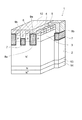
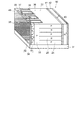
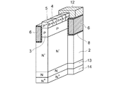
図1は、第1実施形態に係る半導体装置の構造を模式的に示す部分断面図である。ここでは、半導体装置の例としてMOSFET1を取り上げて説明するが、IGBTおよびIEGT等、他の半導体装置にも適用可能である。
[First Embodiment]
FIG. 1 is a partial cross-sectional view schematically showing the structure of the semiconductor device according to the first embodiment. Here,
図1に示すように、本実施形態に係る半導体装置は、N型のドリフト領域2と、ドリフト領域2に接して設けられたP型の第1半導体領域であるベース領域3と、を備えている。また、ベース領域3を挟んでドリフト領域2に対向する主電極であるソース電極12が設けられ、ベース領域3に電気的に接続される。一方、ドリフト領域2とベース領域3との境界には、トレンチ構造の複数の第1ゲート電極であるゲート電極6が境界に沿って設けられる。第1ゲート電極は、ドリフト領域2とベース領域3とに第1のゲート絶縁膜であるゲート絶縁膜8aを介して接している。
As shown in FIG. 1, the semiconductor device according to the present embodiment includes an N-
さらに、2つのゲート電極6の間において、トレンチ構造の第2ゲート電極であるゲート電極7が、ドリフト領域2とベース領域3との境界に沿って、ドリフト領域2とベース領域3とに第2のゲート絶縁膜であるゲート絶縁膜8bを介して接するように設けられている。ゲート電極7は、ドリフト領域2とベース領域3との間の境界からソース電極12に向かう方向において、ベース領域3に接する長さがゲート電極6よりも短く設けられている。
Furthermore, between the two
また、ソース電極12は、2つのゲート電極6の間において、ソース電極からゲート電極7に向かう方向に設けられたトレンチ9bの中に、ゲート電極7に近接した位置まで延在している。さらに、ソース電極12は、ゲート電極6のソース電極12側の端と、ゲート電極7のソース電極12側の端と、の間において、トレンチ9bの内壁面に露出したベース領域3に接している。
The
さらに、図1のソース電極12を除いた部分に示すように、本実施形態に係るMOSFET1では、ベース領域3とソース電極12との間に、N型の第2半導体領域であるソース領域4とP型のコンタクト領域5とが、選択的に設けられている。トレンチ9aの中に設けられたゲート電極6は、ゲート絶縁膜8aを介してドリフト領域2、ベース領域3およびソース領域4に接しており、ベース領域3とゲート絶縁膜8aとの界面に形成されるチャネルを制御する。一方、トレンチ9bでは、ソース電極12がゲート電極7に向かって延在し、トレンチ9bの内壁面に露出した、ソース領域4とドリフト領域2との間のベース領域3に接している。
Further, as shown in the portion excluding the
例えば、図16に示す従来のMOSFETでは、トレンチ内に設けられた全てのゲート電極6が、ゲート絶縁膜8を介してドレイン領域2、ベース領域3およびソース領域4に接している。したがって、例えば、ドリフト領域2からベース領域3に注入される正孔は、ベース領域3の上に選択的に設けられたコンタクト領域5を介してソース電極12に排出される。これに対し、本実施形態に係るMOSFET1では、ゲート電極7を設けることにより、トレンチ9bの内壁面に露出したベース領域3から直接ソース電極12へ正孔を排出できる構成となっている。
For example, in the conventional MOSFET shown in FIG. 16, all the
また、ドリフト領域2のベース領域3に接する面の反対側には、ドリフト領域2よりもN型不純物の濃度が高いN型半導体領域13とN型のドレイン領域14が設けられている。さらに、図示しないドレイン電極が、ドレイン領域14に電気的に接続されて設けられている。ここで、例えば、ドレイン領域14をP型不純物がドープされた半導体領域とすれば、図1は、IGBTまたはIEGTの構造となる。
An N-
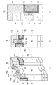
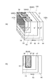
図2は、第1実施形態に係るMOSFET1の動作を説明する模式図である。図2(a)は、MOSFET1の断面構造の一部を模式的に示している。図2(b)および(c)は、MOSFETの動作を示す断面図である。
FIG. 2 is a schematic diagram for explaining the operation of the
MOSFET1のON抵抗を小さくするためには、図2(a)に示すゲート電極6およびゲート電極7の間のベース領域3の幅WCを狭くして、MOSFET1に含まれるゲート電極6の数を増やすことができる。これにより、ゲート絶縁膜8とベース領域3との界面に形成される電流チャネルの数を増やすことができ、ON抵抗を低減することが可能となる。
To reduce the ON resistance of MOSFET1 is to reduce the width W C of the
一方、ベース領域3の幅WCが狭くなると、ベース領域3に含まれるP型不純物の量が少なくなる。例えば、200nm以下まで微細化すると、ベース領域3に含まれるP型不純物の量に対して、ドリフト領域2からベース領域3に注入される正孔の量が無視できなくなる。すなわち、ベース領域3とゲート絶縁膜8との界面に形成される電流チャネルが影響を受けるという問題が生じる。例えば、プラスチャージを持つ正孔が注入されると、ベース領域3のP型のキャリア濃度が実質的に変化し閾値電圧VTHが変動する。このため、ゲート電極に印加するゲート電圧によってソース−ドレイン間に流れる電流を制御できなくなることがある。
On the other hand, if the width W C of the
したがって、ベース領域3の幅WCを狭く形成する場合には、ベース領域3に正孔が蓄積されないように、P型のコンタクト領域5を介してソース電極12へ正孔をスムーズに排出させる必要がある。例えば、図16に示す従来のMOSFETのように、ゲート電極6がソース領域4およびコンタクト領域5に隣接し、ベース領域3を挟んでゲート電極6と左右対称に設けられているような構造では、ベース領域3に注入された正孔は、コンタクト領域5を介してソース電極12に移動する。このため、コンタクト領域5の幅WPを広く設ける必要があるが、そうするとソース領域4の幅WNが相対的に狭くなりON抵抗が増加してしまう。
Therefore, in the case of narrower width W C of the
そこで、本実施形態に係るMOSFETでは、ゲート電極7がベース領域3に隣接する長さが、ゲート電極6がベース領域3に隣接する長さよりも短くなるように、ゲート電極7がゲート絶縁膜8bを介してドリフト領域2とベース領域3の一部に隣接するように設ける。これにより、ソース電極12がゲート電極7とソース領域4との間に露出したベース領域3の一部に接する構造としている。
Therefore, in the MOSFET according to the present embodiment, the
図2(b)に示すように、ドリフト領域2からベース領域3に注入された正孔は、ゲート電極7とソース領域4との間のベース領域3と、ソース電極12と、がコンタクトする部分からソース電極12へと排出される。したがって、ソース電極12がベース領域3にコンタクトする部分の、ソース領域4からドリフト領域2へ向かう方向の幅d1を広くした方が、正孔の排出がよりスムーズになる。例えば、d1>0.05μmとすることができる。
As shown in FIG. 2B, the holes injected from the
これにより、正孔がベース領域3に蓄積されることがなく、VTHの変動を抑えることが可能となる。また、ドリフト領域2からベース領域3を介してソース電極12へ排出される正孔の排出抵抗が小さくなることから、ドリフト領域2で発生する正孔をスムーズに排出してアバランシェ耐量を向上させる効果も得られる。
This prevents the holes are accumulated in the
一方、本実施形態に係るMOSFETでは、ゲート電極7がソース領域4から離間するため、ゲート電極7とベース領域3の間に形成されるチャネルを介してソース領域4からドリフト層2へ直接流れる電流パスが無くなるという不利な効果も生じる。しかしながら、ベース領域3の幅WCを狭くした場合には、図2(b)中に示すように、ゲート電極7側のチャネルを介して流れる電流IN2も、ゲート電極6側の電流チャネルを流れる電流IN1に合流して寄与するので、チャネル抵抗が低くなりON抵抗を低減する効果が得られるようになる。
On the other hand, in the MOSFET according to the present embodiment, since the
上記の本実施態様に係るMOSFETの効果を別の観点から見れば、次のように捉えることができる。すなわち、コンタクト領域5とベース領域3とを合わせたP型領域にソース電極12が接触する面積を比較した場合、ゲート電極6が埋め込まれたトレンチ9aよりも、ゲート電極7が埋め込まれたトレンチ9bのほうが、ソース電極12が広い面積でP型領域に接触する。したがって、ソース電極12がP型領域に接触する面積を相対的に広くすることが可能となり、ベース領域3からソース電極12へ正孔を効率良く排出することができる。
If the effect of the MOSFET according to the present embodiment is viewed from another viewpoint, it can be grasped as follows. That is, when comparing the area where the
図2(c)は、ゲート電極7とベース領域3との間に形成されるNチャネル16を示す模式図である。ゲート電極7にプラスのゲート電圧が印加されると、ゲート絶縁膜8とベース領域3との界面に電子が引き寄せられた反転層が形成される。同図中に示すように、この反転層は、ゲート電極7のソース領域側の端部でソース電極12方向に広がって形成される。このチャネル端部16aがソース電極12につながると、ソース電極12からドリフト層2に電流パスが形成され、過剰電流が流れてしまう恐れがある。そこで、トレンチ9bの内壁面側のゲート電極7の端部とソース電極との間の間隔d2を、ある程度広くしておくと良い。例えば、d2>0.05μmとすることができる。
FIG. 2C is a schematic diagram showing an
例えば、ゲート電極7の端部とソース電極12との間にd2>0.05μmとなるような厚さのゲート絶縁膜8を形成することもできるし、また、ゲート電極7の端部とソース電極12との間に空隙を設けても良い。
For example, a
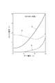
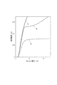
図3は、第1実施形態に係るMOSFET1の特性を示すグラフである。縦軸にソース−ドレイン間に流れるドレイン電流を示し、横軸にゲート電圧を示している。同図中に示すグラフAは、本実施形態に係るMOSFET1の特性を示している。また、グラフBは、ゲート電極7とソース領域4との間でソース電極12がベース領域3と接する部分の幅d1が0.05μmよりも狭い場合のドレイン電流を示している。一方、グラフCは、図16に示す従来のMOSFETの特性を示している。
FIG. 3 is a graph showing the characteristics of the
図3中に示すように、ソース−ドレイン間のバイアス電圧Vdを44V印加しても、ゲート電圧が0Vであれば、グラフAに示す本実施形態に係るMOSFET1ではドレイン電流は流れない。一方、グラフBおよびCに示すMOSFETではドレイン電流が流れる。すなわち、d1<0.05μmとしたグラフBに示すMOSFET、およびグラフCに示す従来のMOSFETでは、ゲート制御が不能となる場合があることを示している。したがって、d1>0.05μmとして、ベース領域3から直接ソース電極12へ正孔を排出する構造とした、本実施形態に係るMOSFET1の方が有利であることがわかる。
As shown in FIG. 3, the source - even when the bias voltage V d between the drain and 44V is applied, when the gate voltage is 0V,
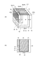
図4は、第1実施形態の変形例に係るMOSFET10の構造を模式的に示す部分断面図である。ソース領域4とゲート電極7との間に露出したベース領域3と、ソース電極12と、が接する部分に、P型不純物濃度がベース領域3よりも高い第3の半導体領域であるP+領域18を設けている点において、図1に示すMOSFET1と異なる。このP+領域18を設けることにより、ソース−ドレイン間に流れる過剰なドレイン電流を抑制することができる。
FIG. 4 is a partial cross-sectional view schematically showing the structure of the
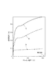
図5および図6は、第1実施形態に係るMOSFET1およびMOSFET10の特性を示すグラフである。縦軸にソース−ドレイン間の負荷がショートした時に流れる短絡電流を示し、横軸にドレイン電圧を示している。同図中のグラフAは、MOSFET1の短絡電流を示し、グラフDは、MOSFET10の短絡電流を示している。また、グラフCは、図16に示す従来のMOSFETの短絡電流を示している。
5 and 6 are graphs showing the characteristics of the
グラフAに示すMOSFET1では、ゲート電極7側に形成されるチャネル16が直接ソース領域4につながっていないため、短絡電流は、ゲート電極6側の電流チャネルに流れる電流と合流してソース領域2に集中して流れる。したがって、ゲート電極7側のチャネルにも電流が流れる従来のMOSFETに比べて、過剰に流れる短絡電流に対する抵抗が大きくなる。その結果、グラフCに示す従来のMOSFETに比べて、短絡電流が約1/2に制限される。これにより、ゲート電極6および7に印加するゲート電圧を0Vとして、短絡電流を遮断することが可能になる。
In the
一方、グラフDに示すMOSFET10では、さらに短絡電流が減少し、従来のMOSFETに比べて約1/5、グラフAに示すMOSFET1の約1/3になっている。これは、ベース領域3に設けられたP+領域18が、電流パスを狭めて短絡電流を制限しているためと考えられる。これにより、ソース−ドレイン間につながれた負荷が短絡したとしても、ゲート電圧によって短絡電流を制御することが容易となる。
On the other hand, in the
図6は、短絡電流とドレイン電圧と関係を示す図5のグラフの低電圧部を拡大して示している。同図中に示すように、短絡電流が0.12A程度までは、従来のMOSFETの特性を示すグラフCとMOSFET1の特性を示すグラフAとは、ほぼ一致している。すなわち、0.12A程度までのドレイン電流に対しては、ゲート電極7側のチャネルをソース領域4から離間して設けたMOSFET1でも、チャネル抵抗は高くならず低いON抵抗を維持できることを示している。
FIG. 6 is an enlarged view of the low voltage portion of the graph of FIG. 5 showing the relationship between the short-circuit current and the drain voltage. As shown in the figure, until the short-circuit current is about 0.12 A, the graph C showing the characteristics of the conventional MOSFET and the graph A showing the characteristics of the
一方、グラフDに示すMOSFET10では、ベース領域3にP+領域18を設けたことにより、チャネル抵抗がやや高くなっているが、短絡電流の抑制効果が高いことがわかる。
On the other hand, in the
図7は、第1実施形態の変形例に係るMOSFET20および30の構造を模式的に示す部分断面図である。
FIG. 7 is a partial cross-sectional view schematically showing the structure of
図7(a)に示すMOSFET20では、ベース領域3の方向にコンタクト領域5をソース領域4よりも深く形成している。これにより、ドリフト層2からベース領域3に注入された正孔をP型のコンタクト領域5を介して排出する経路の排出抵抗を下げることができる。その結果、ベース領域のP型キャリアの濃度変動を抑制して、ゲート電圧によるドレイン電流の制御性を改善することができ、また、ベース領域3とドリフト層2との間のアバランシェ耐量を向上させることもできる。
In the
図7(b)に示すMOSFET30では、図7(a)に示すMOSFET20のベース領域3に、P+領域18をさらに設けた構造となっている。これにより、短絡電流を抑制して短絡耐量を向上させることができる。
The
図8は、第1実施形態の変形例に係るMOSFET40および50の構造を模式的に示す部分断面図である。
FIG. 8 is a partial cross-sectional view schematically showing the structure of
図8(a)に示すMOSFET30では、ソース領域4は、ゲート電極6に沿ってベース領域3の表面に設けられている。これにより、ゲート電極6とベース領域3との間に形成される電流チャネルの全てにソース領域4を接続することができ、チャネル抵抗を下げてON抵抗を低減することができる。
In the
一方、コンタクト領域5は、ソース領域4と並列にゲート電極7の側に形成されている。これにより、ベース領域3から排出される正孔のパスは、ゲート電極7の側でコンタクトするソース電極のみとなるが、コンタクト面積を広くして正孔の排出抵抗を低減することができる。
On the other hand, the
図8(b)に示すMOSFET50では、ベース領域3との間の境界に沿って第5半導体領域であるP型ピラー21と第4半導体領域であるN型ピラー22が交互に配置されたスーパージャンクション構造のドリフト領域2が設けられている。スーパージャンクション構造を用いることにより、N型ピラー22の濃度を上げてON抵抗を低減することが可能となる。
In the
[第2実施形態]
図9は、第2実施形態に係る半導体装置の構造を模式的に示す部分断面図である。本実施形態に係るMOSFET60は、絶縁層31の主面上に設けられた横型構造を有している。なお、絶縁層31は、例えば、基板上に設けられたSiO2等の絶縁膜でも良いし、半絶縁性を有する半導体層であっても良い。
[Second Embodiment]
FIG. 9 is a partial cross-sectional view schematically showing the structure of the semiconductor device according to the second embodiment. The
図9(a)に示すように、MOSFET60は、絶縁層31(または半絶縁層)の主面上に設けられたN型の半導体を含むドリフト領域32と、主面に平行な横方向にドリフト領域32に隣接して設けられたP型の第1半導体領域であるベース領域33と、ベース領域33の横方向に隣接して設けられたN型の第2半導体領域であるソース領域34と、を備えている。また、ソース領域34のベース領域33に接する側面の反対側の側面に接して主電極であるソース電極38が設けられている。
As shown in FIG. 9A, the
また、ドリフト領域32とベース領域33とソース領域34とに跨った表面から絶縁層31方向に、ドリフト領域32とベース領域33との境界に沿って、複数のトレンチ45が形成されている。トレンチ45の中には、第1ゲート電極であるゲート電極35が設けられている。さらに、2つのゲート電極35の間には、ドリフト領域32とベース領域33の一部とに跨った表面から、ドリフト領域32とベース領域33との境界に沿って、絶縁層31の方向にトレンチ46が形成されている。トレンチ46の中には、第2ゲート電極であるゲート電極36が設けられている。したがって、ドリフト領域32とベース領域33との境界からソース電極38に向かう方向において、ゲート電極36がゲート絶縁膜37bを介してベース領域33に接する長さは、ゲート電極35がゲート絶縁膜37aを介してベース領域33に接する長さよりも短く設けられている。
A plurality of
さらに、ソース電極38の一部は、2つのゲート電極35の間で、ソース電極38からゲート電極46に向かう方向に形成されたトレンチ47の中に延在して設けられている。トレンチ47は、ソース領域34とベース領域33の一部とに跨る表面から絶縁層31の方向に形成されている。また、ソース電極38は、トレンチ47の中に、ゲート電極35のソース電極38側の端の位置を超えてゲート電極46に近接した位置まで延在し、ゲート電極36とソース領域34との間のトレンチ47の内壁面に露出したベース領域33に電気的に接続している。
Further, a part of the
また、ドリフト領域32に隣接して、ドリフト領域32よりもN型不純物濃度の高いN型半導体領域41と、N型半導体領域41に隣接してドレイン領域42と、が設けられている。さらに、ドレイン領域42に電気的に接続するドレイン電極43が設けられている。
An N-
また、図9(b)は、図9(a)中に示すIXb−IXb断面を示す模式図である。同図中に示すように、トレンチ45は、絶縁層31に連通して設けることができる。また、トレンチ45の内面にはゲート絶縁膜37aが形成され、さらに、トレンチ45の内部は、例えば、導電性のポリシリコンからなるゲート電極35で埋められている。トレンチ46に形成されるゲート電極36も、同様に形成することができる。また、以下、図12までに示す実施形態に係るMOSFETにおいても同様である。
Moreover, FIG.9 (b) is a schematic diagram which shows the IXb-IXb cross section shown in Fig.9 (a). As shown in the figure, the
本実施形態に係るMOSFET60では、ソース電極38の延在部39が、ソース領域34の表面からベース領域33の表面の一部に跨る表面から絶縁層31に連通するトレンチ47の中に設けられている。これにより、ソース電極38は、ゲート電極36とソース領域34との間のトレンチ47の内面に露出したベース領域33に接触して、ドリフト領域32からベース領域33に注入される正孔を排出することができる。
In the
また、延在部39がベース領域33に接触するコンタクト部分の幅d1を0.05μm以上として、ソース−ドレイン間に流れるドレイン電流がゲート電圧で制御不能となる不具合を防止することが可能である。
Further, the width d1 of the contact portion where the extended
本実施形態に係るMOSFET60は、絶縁層31の上に形成されるドリフト領域32およびベース領域33、ソース領域34等の厚さが薄い場合には、例えば、絶縁層31の上に設けられた半導体層に、N型およびP型の不純物をイオン注入して形成することができる。また、各半導体領域を厚く設ける場合には、複数回のエピタキシャル成長とイオン注入を組み合わせることにより形成することができる。また、図10に説明する横型のMOSFETにおいても同様である。なお、ここで厚さとは、絶縁層31から各半導体領域の表面方向への層厚を意味するものとする。
The
また、本実施形態においても、例えば、ドレイン領域42をP型不純物がドープされたP型半導体領域とすれば、図9は、IGBTまたはIEGTの構造を示している。以下、図12までに示す実施形態についても同様である。
Also in this embodiment, for example, if the
図10は、第2実施形態の変形例に係るMOSFET70の構造を模式的に示す部分断面図である。MOSFET70は、ドリフト領域32において、ドリフト領域32とベース領域33との間の境界に沿って第5の半導体領域であるP型ピラー21と第4の半導体領域であるN型ピラー22とを交互に配置したスーパージャンクション構造を有している。
FIG. 10 is a partial cross-sectional view schematically showing the structure of a
図9に示すMOSFET60と同様に、本変形例に係るMOSFET70においても、ソース電極38の延在部36がベース領域33に接触するゲート電極36とソース領域34との間のコンタクト部分からベース領域33の正孔をソース電極38に排出することができる。これにより、閾値電圧VTHを安定させることができるので、ゲート電極35とゲート電極36との間のベース領域33の幅を狭くすることが可能となる。したがって、MOSFETのチャネル数を増やしてチャネル抵抗を低減することができる。さらに、スーパージャンクション構造を用いることにより、ベース領域33につながるN型ピラー22の濃度を高くしてドリフト領域の抵抗を低減することができる。これにより、MOSFET70のON抵抗を低減することが可能である。
Similarly to the
図11は、第2実施形態の変形例に係るMOSFET80の構造を模式的に示す部分断面図である。同図中に示すように、MOSFET80のドリフト領域32は、絶縁層31から上部方向へPピラーとNピラーが交互に積層されたスーパージャンクション構造を有している。
FIG. 11 is a partial cross-sectional view schematically showing the structure of a
本変形例に係るMOSFET80は、絶縁層31(または半絶縁層)の主面上に、N型の第1半導体層であるN型半導体層24と、P型の第2半導体層であるP型半導体層25と、が交互に設けられた積層体27を備え、ドリフト領域32をスーパージャンクション構造としている。また、積層体27の一方の側面には、第1の主電極であるソース電極38が電気的に接続して設けられ、他方の側面には、第2の主電極であるドレイン電極43が電気的に接続して設けられている。
The
さらに、積層体27は、ソース電極38とドレイン電極43との間に、積層体27の表面から絶縁層31の主面に連通して設けられたP型の第1半導体領域であるベース領域33を有している。さらに、ソース電極38とベース領域33とに挟まれたN型の第2半導体領域であるソース領域34と、ベース領域33とドレイン電極43との間にドリフト領域32と、を有している。
Further, the
また、積層体27には、ソース領域34と、ベース領域33と、ドリフト領域32と、に跨った表面から、絶縁層31の主面に向かってトレンチ45が形成されている。さらに、トレンチ45の中には、第1のゲート電極であるゲート電極35が設けられている。また、ベース領域33の一部と、ドリフト領域32と、に跨った表面から、絶縁層31の主面に向かってトレンチ46が設けられ、トレンチ46の中には、第2のゲート電極であるゲート電極36が設けられている。
In the
2つのゲート電極35の間には、ソース領域34とベース領域33の一部とに跨る表面から絶縁層31主面に向かってトレンチ47が形成されており、トレンチ47の中には、ソース電極38が延在している。延在39は、ソース領域34とゲート電極36との間のトレンチ47の内壁面に露出したベース領域33に接するように設けられている。
A
これにより、ドリフト領域32からベース領域33へ注入される正孔がソース電極38へ排出されるので、閾値電圧VTHが安定する。また、アバランシェ耐量および短絡耐量を向上させることができる。
Thereby, the holes injected from the
一方、ドリフト領域32とドレイン電極43との間には、積層体27の表面から絶縁層31に連通して、N型半導体領域41とドレイン領域42とが設けられている。ドレイン領域42は、N型不純物が高濃度にドープされたN+領域である。本変形例においても、ドレイン領域42にP型不純物をドープしてP+領域とし、IGBTまたはIEGTとすることができる。
On the other hand, an N-
積層体27は、複数回のエピタキシャル成長により絶縁層31の上に複数の半導体層を設け、さらに、各エピタキシャル成長の間に、P型およびN型の不純物を、選択的に所定の場所にイオン注入することにより形成することができる。
In the
図12は、第2実施形態の変形例に係るMOSFET90の構造を模式的に示す部分断面図である。MOSFET90は、図11に示すMOSFET80のソース領域34が、P+コンタクト領域51とN+ソース領域52の積層構造に置き換えられた構成となっている。これにより、ベース領域33の正孔をP+コンタクト領域51を介してソース電極38に排出することができる。P+コンタクト領域51とN+ソース領域52は、ぞれぞれイオン注入によって形成することができる。
FIG. 12 is a partial cross-sectional view schematically showing the structure of a
また、P+コンタクト領域51とN+ソース領域52の積層方向の厚さは、イオン注入する不純物のドーズ量により変えることができる。例えば、P+コンタクト領域51に注入するP型不純物のドーズ量をN+ソース領域52に注入するN型不純物のドーズ量よりも多くすると、図12中に示すように、P+コンタクト領域51をN+ソース領域52よりも厚くすることができる。これにより、ベース領域33からソース電極38への正孔の排出抵抗を小さくすることができる。また、N+ソース領域52に注入するN型不純物のドーズ量を増やせば、N+ソース領域52を厚くしてON抵抗を低減することもできる。
Further, the thickness in the stacking direction of the P + contact region 51 and the N + source region 52 can be changed depending on the dose amount of the impurity to be ion-implanted. For example, when the dose amount of the P-type impurity implanted into the P + contact region 51 is made larger than the dose amount of the N-type impurity implanted into the N + source region 52, the P + contact region 51 is formed as shown in FIG. It can be made thicker than the N + source region 52. Thereby, the discharge resistance of holes from the
また、MOSFET90では、ゲート絶縁膜37を介してゲート電極35に隣接してソース電極38の延在部49が設けられているが、図10に示すMOSFET70のように、延在部49を設けないで、ゲート電極35とソース電極38との間にP+コンタクト領域51とN+ソース領域52を介在させても良い。
In the
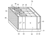
[第3実施形態]
図13は、第3実施形態に係るMOSFET100の構造を模式的に示す部分断面図である。
[Third Embodiment]
FIG. 13 is a partial cross-sectional view schematically showing the structure of the
MOSFET100は、N型不純物が高濃度にドープされた半導体層であるドレイン層44の第1の主面61に設けられたN型のドリフト領域32と、ドリフト領域32の中に設けられたP型の第1半導体領域であるベース領域33と、ベース領域33の中に設けられたN型の第2半導体領域であるソース領域34と、を備えている。
ここでドレイン層44として、例えば、シリコン基板上に形成されたN型半導体層を用いることもできるし、N型不純物が高濃度にドープされたシリコン基板を用いても良い。また、ドレイン層44に代えてP型半導体層を用いると、IGBTまたはIEGTとすることができる。
Here, as the
図13に示す半導体領域の構成は、例えば、所定の凹部が設けられたドレイン層44の第1の主面61に、N型半導体領域41となる半導体層、およびドリフト領域32となる半導体層、ベース領域33となる半導体層、ソース領域34となる半導体層を順次エピタキシャル成長し、さらに、各半導体層が設けられたドレイン層44の第1の主面61をCMP(Chemical Mechanical Polish)を用いて平坦化することにより形成することができる。
The configuration of the semiconductor region shown in FIG. 13 includes, for example, a semiconductor layer that becomes the N-
複数のトレンチ45が、ドリフト領域32とベース領域33との境界に沿ってドレイン層44の第2の主面62に向けて形成されている。また、トレンチ45の中には、第1のゲート電極であるゲート電極35が設けられている。一方、2つのゲート電極35の間には、第トレンチ46が、ドリフト領域32とベース領域33の境界に沿ってドレイン層44の第2の主面62に向けて設けられている。さらに、トレンチ46の中には、第2のゲート電極であるゲート電極36が設けられている。
A plurality of
また、主電極であるソース電極38が、ソース領域34に接して設けられている。ソース電極38は、例えば、ゲート電極35の配列に沿ってソース領域34の表面からベース領域33に連通するトレンチ55の中に設けることができる。さらに、2つのゲート電極35の間に、ソース領域34とベース領域33の一部とに跨る表面からソース領域34とベース領域62の境界に沿ってトレンチ55の拡張部分が設けられている。ソース電極38は、ゲート電極36に向かってトレンチ55の拡張部分に延在して設けられている。延在部39は、ソース領域34とゲート電極36との間のトレンチ55の張り出し部の内壁面に露出した、ベース領域33に接して設けられている。
A
図13(b)は、図13(a)中に示されたXIIIb−XIIIb断面の構造を示す模式図である。トレンチ45は、表面からドリフト領域32とベース領域33の境界に沿ってベース領域33およびソース領域34を貫通し、下方のドリフト領域32に達するように形成されている。また、トレンチ45の内面にはゲート絶縁膜37が形成され、ゲート電極35となる、例えば、導電性のポリシリコンが埋め込まれている。
FIG. 13B is a schematic diagram showing the structure of the XIIIb-XIIIb cross section shown in FIG. The
本実施形態に係るMOSFET100においても、ソース電極38の延在部39が、ゲート電極36とソース領域34との間のトレンチ55の拡張部の内面に露出したベース領域33に接触しており、ドリフト領域32からベース領域33に注入される正孔をソース電極38へ排出することができる。
Also in the
図14(a)は、第3実施形態の変形例に係るMOSFET110の構造を模式的に示す部分断面図である。また、図14(b)は、図14(a)中に示したXIVb−XIVb断面の構造を示す模式図である。
FIG. 14A is a partial cross-sectional view schematically showing the structure of a
MOSFET110は、トレンチ45およびトレンチ46がドレイン層44に達するように設けられ、ゲート電極35およびゲート電極36が埋め込まれている点で、図13に示すMOSFET100と異なる。
すなわち、図14(a)に示すように、トレンチ45は、ソース領域34およびベース領域33、ドリフト領域32、N型半導体領域41、ドレイン層44に跨ったドレイン層44の第1の主面61側の表面から、第2の主面62方向に設けられている。また、図14(b)に示すように、トレンチ45は、ソース領域34およびベース領域33、ドリフト領域32、N型半導体領域41、を貫通してドレイン層44に達するように設けられている。さらに、トレンチ45の内面には、ゲート絶縁膜37が形成され、ゲート電極35となる、例えば、導電性のポリシリコンが埋め込まれている。
That is, as shown in FIG. 14A, the
一方、ゲート電極36が設けられているトレンチ46も、ベース領域33およびドリフト領域32、N型半導体領域41、ドレイン層44に跨ったドレイン層44の第1の主面61側の表面から、第2の主面62側のドレイン層44に達するように設けられている。
On the other hand, the
MOSFET110では、ゲート電極35および36にプラスのゲート電圧が印加されると、ドリフト領域32と、ゲート絶縁膜37との界面に電子が蓄積したチャネルが形成される。これにより、ドリフト領域32の抵抗が下がり、ON抵抗を低減することができる。
In
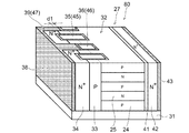
[第4実施形態]
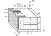
図15は、第4実施形態に係る半導体装置120の構造を模式的に示す部分断面図である。半導体装置120は、絶縁層31の主面に交互に積層された複数のP型半導体領域24およびN型半導体領域25からなるスーパージャンクション構造を有する電力制御用半導体装置である。
[Fourth Embodiment]
FIG. 15 is a partial cross-sectional view schematically showing the structure of the
半導体装置120は、絶縁層31(または半絶縁層)の主面上に、N型半導体領域25と、P型半導体領域24と、が交互に設けられた積層体27を有している。積層体27の一方の側面には、第1の主電極であるソース電極38が電気的に接続して設けられている。また、積層体27の他方の側面には、第2の主電極であるドレイン電極43が電気的に接続して設けられている。
The
さらに、ソース電極38とドレイン電極43との間に、P型半導体領域24とN型半導体領域25とが交互に積層されたスーパージャンクション構造のドリフト領域32が設けられている。ドリフト領域32とソース電極38との間には、P型の不純物がP型半導体領域24よりも高濃度にドープされた第2半導体領域であるP+領域54と、N型の不純物がN型半導体領域25よりも高濃度にドープされたN+領域53と、を積層したコンタクト領域58が設けられている。
Furthermore, a
また、コンタクト領域58とドリフト領域32とに跨った表面から、コンタクト領域58とドリフト領域32との境界に沿って、トレンチ45が形成されている。トレンチ45の中には、第1のゲート電極であるゲート電極35が設けられている。さらに、コンタクト領域51の一部と、ドリフト領域32と、に跨った表面から、コンタクト領域58とドリフト領域32との境界に沿ってトレンチ46が形成されている。トレンチ46の中には、第2のゲート電極であるゲート電極36が設けられている。
A
半導体装置120のソース電極38は、コンタクト領域58のP+領域54とN+領域53に電気的に接続されている。ソース電極38の一部である延在部39は、2つのゲート電極35の間で、ソース電極38からゲート電極36の近傍に至るP+領域54の表面から、絶縁層31の主面に向かって形成されたトレンチ47の中に延在して設けられている。また、延在部39は、トレンチ47の内壁面に露出したコンタクト領域58に電気的に接続されている。また、ゲート電極35にゲート絶縁膜37を介して隣接する延在部49も設けられている。
The source electrode 38 of the
一方、ドリフト領域32とドレイン電極43との間には、N型半導体領域41とドレイン領域42とが、表面から絶縁層31の主面に連通して設けられている。本実施態様に係る半導体装置120では、ドレイン領域42は、N型不純物が高濃度にドープされたN+領域であるが、P型不純物をドープしてP+領域としても良い。その場合には、半導体装置120は、バイポーラ素子として動作する。
On the other hand, an N-
また、積層体27は、絶縁層31の主面に複数回のエピタキシャル成長により、N型半導体領域25とP型半導体領域24とを積層することによって形成することができる。また、各半導体領域のエピタキシャル成長の間に、イオン注入を用いて選択的にP型およびN型の不純物を注入することによって、上記の積層構造とすることができる。
The
次に、半導体装置120の動作について説明する。半導体装置120では、コンタクト領域58において、N+領域53の積層方向の幅は、P+領域54よりも狭く設ける。さらに、P+領域54とN+領域53との間のPN接合のビルトインポテンシャルにより、N+領域53を空乏化させる。これにより、ドレイン電極43とソース電極38との間にドレイン側がプラスとなるドレイン電圧を印加しても、ゲート電極35および36にゲート電圧が印加されない状態では、ドレイン電流は流れない。
Next, the operation of the
次に、ゲート電極35および36にプラスのゲート電圧を印加すると、N+領域53とゲート絶縁膜37との間に電子が蓄積されて電流チャネルが形成される。これにより、ドレイン電極43とソース電極38との間に電流がながれON状態となる。
Next, when a positive gate voltage is applied to the
この際、N+領域53にドリフト領域32のN型半導体層25から正孔が注入されると、N+領域53の実効的な濃度が変化してチャネル抵抗が高くなりON抵抗が上昇してしまう場合がある。
In this case, the positive holes from the N-
これに対し半導体装置120では、ソース電極38がトレンチ47の内壁面に露出したコンタクト領域58のN+領域53に電気的に接続されているので、N+領域53に注入された正孔をソース電極38へスムーズに排出することができる。これにより、N+領域53の実効的なキャリア濃度の変動を抑制して、半導体装置120を安定に動作させることができる。また、アバランシェ耐量を向上させることができる。
In contrast, in the
以上、本発明に係る第1〜第4の実施形態を参照して本発明を説明したが、本発明はこれらの実施形態に限定されるものではない。例えば、出願時の技術水準に基づいて、当業者がなし得る設計変更や、材料の変更等、本発明と技術的思想を同じとする実施態様も本発明の技術的範囲に含有される。 Although the present invention has been described with reference to the first to fourth embodiments according to the present invention, the present invention is not limited to these embodiments. For example, embodiments that have the same technical idea as the present invention, such as design changes and material changes that can be made by those skilled in the art based on the technical level at the time of filing, are also included in the technical scope of the present invention.
2 ドリフト領域
3、33 ベース領域
4、34、52 ソース領域
5、51、58 コンタクト領域
6、7、35、36 ゲート電極
8、8a、8b、37、37a、37b ゲート絶縁膜
9a、9b トレンチ
12、38 ソース電極
13 N型半導体層
14 ドレイン層
18、54 P+領域
21 P型ピラー
22 N型ピラー
24 P型半導体領域
25 N型半導体領域
27 積層体
31 絶縁層
32 ドリフト領域
39、49 張り出し部
41 N型半導体領域
42 ドレイン領域
43 ドレイン電極
44 ドレイン層
45、46、47、55 トレンチ
53 N+領域
61 第1の主面
62 第2の主面
1、10、20、30、40,50,60,70,80、90 MOSFET
100、110、MOSFET
120 半導体装置
2
100, 110, MOSFET
120 Semiconductor device
Claims (7)
前記第1電極上に設けられた第1導電型の第1半導体領域と、
前記第1半導体領域上に設けられた第2導電型の第2半導体領域と、
前記第1半導体領域上に位置し、前記第1電極から前記第1半導体領域に向かう第1方向に直交する第2方向において複数設けられた第2電極と、
前記第1半導体領域上に位置し、前記第2方向において前記第2電極間に設けられた第3電極と、
を有し、前記第1方向における前記第2電極の上面から前記第1電極までの長さが、前記第1方向における前記第3電極の上面から前記第1電極までの長さよりも大きい半導体装置。 A first electrode;
A first semiconductor region of a first conductivity type provided on the first electrode;
A second semiconductor region of a second conductivity type provided on the first semiconductor region;
A plurality of second electrodes located on the first semiconductor region and provided in a second direction orthogonal to the first direction from the first electrode toward the first semiconductor region;
A third electrode located on the first semiconductor region and provided between the second electrodes in the second direction;
And a length from the upper surface of the second electrode to the first electrode in the first direction is larger than a length from the upper surface of the third electrode to the first electrode in the first direction. .
Priority Applications (1)
| Application Number | Priority Date | Filing Date | Title |
|---|---|---|---|
| JP2015112383A JP6089070B2 (en) | 2015-06-02 | 2015-06-02 | Semiconductor device |
Applications Claiming Priority (1)
| Application Number | Priority Date | Filing Date | Title |
|---|---|---|---|
| JP2015112383A JP6089070B2 (en) | 2015-06-02 | 2015-06-02 | Semiconductor device |
Related Parent Applications (1)
| Application Number | Title | Priority Date | Filing Date |
|---|---|---|---|
| JP2010042235A Division JP5762689B2 (en) | 2010-02-26 | 2010-02-26 | Semiconductor device |
Publications (2)
| Publication Number | Publication Date |
|---|---|
| JP2015173291A true JP2015173291A (en) | 2015-10-01 |
| JP6089070B2 JP6089070B2 (en) | 2017-03-01 |
Family
ID=54260394
Family Applications (1)
| Application Number | Title | Priority Date | Filing Date |
|---|---|---|---|
| JP2015112383A Expired - Fee Related JP6089070B2 (en) | 2015-06-02 | 2015-06-02 | Semiconductor device |
Country Status (1)
| Country | Link |
|---|---|
| JP (1) | JP6089070B2 (en) |
Cited By (1)
| Publication number | Priority date | Publication date | Assignee | Title |
|---|---|---|---|---|
| JP2020025050A (en) * | 2018-08-08 | 2020-02-13 | 株式会社東芝 | Semiconductor device |
Citations (3)
| Publication number | Priority date | Publication date | Assignee | Title |
|---|---|---|---|---|
| JP2009038214A (en) * | 2007-08-01 | 2009-02-19 | Toshiba Corp | Semiconductor device |
| JP2010505270A (en) * | 2006-09-27 | 2010-02-18 | マックスパワー・セミコンダクター・インコーポレイテッド | Power MOSFET with recessed field plate |
| JP2011165928A (en) * | 2010-02-10 | 2011-08-25 | Toyota Central R&D Labs Inc | Insulated gate bipolar transistor |
-
2015
- 2015-06-02 JP JP2015112383A patent/JP6089070B2/en not_active Expired - Fee Related
Patent Citations (3)
| Publication number | Priority date | Publication date | Assignee | Title |
|---|---|---|---|---|
| JP2010505270A (en) * | 2006-09-27 | 2010-02-18 | マックスパワー・セミコンダクター・インコーポレイテッド | Power MOSFET with recessed field plate |
| JP2009038214A (en) * | 2007-08-01 | 2009-02-19 | Toshiba Corp | Semiconductor device |
| JP2011165928A (en) * | 2010-02-10 | 2011-08-25 | Toyota Central R&D Labs Inc | Insulated gate bipolar transistor |
Cited By (2)
| Publication number | Priority date | Publication date | Assignee | Title |
|---|---|---|---|---|
| JP2020025050A (en) * | 2018-08-08 | 2020-02-13 | 株式会社東芝 | Semiconductor device |
| JP7005453B2 (en) | 2018-08-08 | 2022-01-21 | 株式会社東芝 | Semiconductor device |
Also Published As
| Publication number | Publication date |
|---|---|
| JP6089070B2 (en) | 2017-03-01 |
Similar Documents
| Publication | Publication Date | Title |
|---|---|---|
| JP5762689B2 (en) | Semiconductor device | |
| US9362393B2 (en) | Vertical semiconductor device including element active portion and voltage withstanding structure portion, and method of manufacturing the vertical semiconductor device | |
| US9276076B2 (en) | Semiconductor device | |
| JP2016167519A (en) | Semiconductor device | |
| JP5480084B2 (en) | Semiconductor device | |
| JP6356803B2 (en) | Insulated gate bipolar transistor | |
| JP5537359B2 (en) | Semiconductor device | |
| JP2013258333A (en) | Power semiconductor device | |
| US9502547B2 (en) | Charge reservoir IGBT top structure | |
| JP2014216572A (en) | Semiconductor device | |
| JP2016115847A (en) | Semiconductor device | |
| JP2011233701A (en) | Power semiconductor device | |
| JP2016058428A (en) | Semiconductor device | |
| TW201803125A (en) | Vertical niobium metal oxide semiconductor field effect transistor | |
| JP2015201615A (en) | Semiconductor device and method of manufacturing the same | |
| US20140084334A1 (en) | Power semiconductor device | |
| JP6299658B2 (en) | Insulated gate type switching element | |
| US20120241817A1 (en) | Semiconductor device | |
| JP2016062975A (en) | Semiconductor device and method of manufacturing the same | |
| JP6173987B2 (en) | Semiconductor device | |
| JP2014154739A (en) | Semiconductor device | |
| JP6089070B2 (en) | Semiconductor device | |
| JP6458994B2 (en) | Semiconductor device | |
| KR101397784B1 (en) | Insulated gate bipolar transistor | |
| US9502498B2 (en) | Power semiconductor device |
Legal Events
| Date | Code | Title | Description |
|---|---|---|---|
| A131 | Notification of reasons for refusal |
Free format text: JAPANESE INTERMEDIATE CODE: A131 Effective date: 20160727 |
|
| A977 | Report on retrieval |
Free format text: JAPANESE INTERMEDIATE CODE: A971007 Effective date: 20160729 |
|
| A521 | Request for written amendment filed |
Free format text: JAPANESE INTERMEDIATE CODE: A523 Effective date: 20160923 |
|
| A131 | Notification of reasons for refusal |
Free format text: JAPANESE INTERMEDIATE CODE: A131 Effective date: 20161013 |
|
| A521 | Request for written amendment filed |
Free format text: JAPANESE INTERMEDIATE CODE: A523 Effective date: 20161208 |
|
| TRDD | Decision of grant or rejection written | ||
| A01 | Written decision to grant a patent or to grant a registration (utility model) |
Free format text: JAPANESE INTERMEDIATE CODE: A01 Effective date: 20170105 |
|
| A61 | First payment of annual fees (during grant procedure) |
Free format text: JAPANESE INTERMEDIATE CODE: A61 Effective date: 20170206 |
|
| R151 | Written notification of patent or utility model registration |
Ref document number: 6089070 Country of ref document: JP Free format text: JAPANESE INTERMEDIATE CODE: R151 |
|
| LAPS | Cancellation because of no payment of annual fees |