JP2015149700A5 - - Google Patents
Download PDFInfo
- Publication number
- JP2015149700A5 JP2015149700A5 JP2014023137A JP2014023137A JP2015149700A5 JP 2015149700 A5 JP2015149700 A5 JP 2015149700A5 JP 2014023137 A JP2014023137 A JP 2014023137A JP 2014023137 A JP2014023137 A JP 2014023137A JP 2015149700 A5 JP2015149700 A5 JP 2015149700A5
- Authority
- JP
- Japan
- Prior art keywords
- light
- guide plate
- light guide
- deflecting
- emitted
- Prior art date
- Legal status (The legal status is an assumption and is not a legal conclusion. Google has not performed a legal analysis and makes no representation as to the accuracy of the status listed.)
- Granted
Links
- 230000003287 optical Effects 0.000 claims description 19
- 230000001902 propagating Effects 0.000 claims description 5
- 239000011159 matrix material Substances 0.000 claims description 3
- 230000000644 propagated Effects 0.000 claims 8
- 238000001514 detection method Methods 0.000 claims 4
- 229910002601 GaN Inorganic materials 0.000 claims 3
- 239000004065 semiconductor Substances 0.000 claims 3
- 239000004973 liquid crystal related substance Substances 0.000 description 11
- 230000000051 modifying Effects 0.000 description 2
- 230000001070 adhesive Effects 0.000 description 1
- 239000000853 adhesive Substances 0.000 description 1
- 210000002858 crystal cell Anatomy 0.000 description 1
- 239000004615 ingredient Substances 0.000 description 1
Images

Description
あるいは又、実施例1あるいは後述する実施例2〜実施例11において、受光装置126,326,127,327,128,328,825は、光学装置120,320,520,820に対して光学的に接続されている。即ち、受光装置126,326,127,327,128,328,825は、光学装置120,320,520,820に直接接続されている形態のみならず、接着部材や導光部材等を介して光が入るように接続されている形態も包含される。また、受光装置126,326,127,327,128,328,825が検出する光は、画像形成装置111,211から出射された光の一部、又は、光学装置120,320,520,820が伝播する光の一部であれば足りる。
Alternatively, in the first embodiment or the second to eleventh embodiments described later, the light
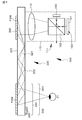
実施例1あるいは後述する実施例4において、画像形成装置111は、第1の構成の画像形成装置であり、2次元マトリクス状に配列された複数の画素を有する。具体的には、画像形成装置111は、反射型空間光変調装置150、及び、白色光を出射する発光ダイオードから成る光源153から構成されている。各画像形成装置111全体は、筐体113(図1では、一点鎖線で示す)内に納められており、係る筐体113には開口部(図示せず)が設けられており、開口部を介して光学系(平行光出射光学系,コリメート光学系)112から光が出射される。反射型空間光変調装置150は、ライト・バルブとしてのLCOSから成る液晶表示装置(LCD)151、及び、光源153からの光の一部を反射して液晶表示装置151へと導き、且つ、液晶表示装置151によって反射された光の一部を通過させて光学系112へと導く偏光ビームスプリッター152から構成されている。液晶表示装置151は、2次元マトリクス状に配列された複数(例えば、640×480個)の画素(液晶セル)を備えている。偏光ビームスプリッター152は、周知の構成、構造を有する。光源153から出射された無偏光の光は、偏光ビームスプリッター152に衝突する。偏光ビームスプリッター152において、P偏光成分は通過し、系外に出射される。一方、S偏光成分は、偏光ビームスプリッター152において反射され、液晶表示装置151に入射し、液晶表示装置151の内部で反射され、液晶表示装置151から出射される。ここで、液晶表示装置151から出射した光の内、「白」を表示する画素から出射した光にはP偏光成分が多く含まれ、「黒」を表示する画素から出射した光にはS偏光成分が多く含まれる。従って、液晶表示装置151から出射され、偏光ビームスプリッター152に衝突する光の内、P偏光成分は、偏光ビームスプリッター152を通過し、光学系112へと導かれる。一方、S偏光成分は、偏光ビームスプリッター152において反射され、光源153に戻される。光学系112は、例えば、凸レンズから構成され、平行光を生成させるために、光学系112における焦点距離の所(位置)に画像形成装置111(より具体的には、液晶表示装置151)が配置されている。
In Example 1 or Example 4 described later, the
Claims (13)
(B)画像形成装置から出射された光が入射され、出射される光学装置、及び、
(C)画像形成装置から出射された光を検出する受光装置、
を備えている画像表示装置。 (A) an image forming apparatus,
(B) an optical device that receives and emits light emitted from the image forming apparatus; and
(C) a light receiving device that detects light emitted from the image forming apparatus;
An image display device comprising:
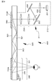
(a)入射された光が内部を全反射により伝播した後、出射される導光板、
(b)導光板に入射された光が導光板の内部で全反射されるように、導光板に入射された光を偏向させる第1偏向手段、及び、
(c)導光板の内部を全反射により伝播した光の一部を導光板から出射させるために、導光板の内部を全反射により伝播した光を偏向させる第2偏向手段、
を備えており、
第2偏向手段は、
導光板の内部を全反射により伝播した光を観察者に向かって偏向させる第1の部分、及び、
導光板の内部を全反射により伝播した光を受光装置に向かって偏向させる第2の部分、
から構成されている請求項1に記載の画像表示装置。 The optical device
(A) A light guide plate that is emitted after incident light propagates through the interior by total reflection;
(B) first deflecting means for deflecting the light incident on the light guide plate so that the light incident on the light guide plate is totally reflected inside the light guide plate; and
(C) second deflecting means for deflecting the light propagated in the light guide plate by total reflection in order to emit a part of the light propagated in the light guide plate by total reflection from the light guide plate;
With
The second deflection means is
A first portion for deflecting light propagating in the light guide plate by total reflection toward an observer; and
A second portion for deflecting light propagating through the internal reflection of the light guide plate toward the light receiving device;
The image display device according to claim 1, comprising:
(a)入射された光が内部を全反射により伝播した後、出射される導光板、
(b)導光板に入射された光が導光板の内部で全反射されるように、導光板に入射された光を偏向させる第1偏向手段、及び、
(c)導光板の内部を全反射により伝播した光の一部を導光板から出射させるために、導光板の内部を全反射により伝播した光を偏向させる第2偏向手段、
を備えており、
受光装置は、導光板の第2偏向手段側の端部に配置されている請求項1に記載の画像表示装置。 The optical device
(A) A light guide plate that is emitted after incident light propagates through the interior by total reflection;
(B) first deflecting means for deflecting the light incident on the light guide plate so that the light incident on the light guide plate is totally reflected inside the light guide plate; and
(C) second deflecting means for deflecting the light propagated in the light guide plate by total reflection in order to emit a part of the light propagated in the light guide plate by total reflection from the light guide plate;
With
The image display device according to claim 1, wherein the light receiving device is disposed at an end portion of the light guide plate on the second deflecting unit side.
受光装置は、光半反射部材を通過した光を検出する請求項1に記載の画像表示装置。 The optical device includes a light semi-reflective member that reflects part of the light emitted from the image forming apparatus and passes through the remaining part.
The image display device according to claim 1, wherein the light receiving device detects light that has passed through the light semi-reflective member.
光学装置は、
(a)入射された光が内部を全反射により伝播した後、出射される導光板、
(b)導光板に入射された光が導光板の内部で全反射されるように、導光板に入射された光を偏向させる、反射鏡又は半透過鏡から成る第1偏向手段、及び、
(c)導光板の内部を全反射により伝播した光の一部を導光板から出射させるために、導光板の内部を全反射により伝播した光を偏向させる、反射型体積ホログラム回折格子から成る第2偏向手段、
を備えており、
第2偏向手段は、
導光板の内部を全反射により伝播した光を観察者に向かって偏向させる第1の部分、及び、
導光板の内部を全反射により伝播した光を受光装置に向かって偏向させる第2の部分、
から構成されており、
受光装置の検出結果に基づき、光源から出射される光の波長を制御する請求項1に記載の画像表示装置。 The image forming apparatus includes a light source composed of a GaN-based semiconductor laser element,
The optical device
(A) A light guide plate that is emitted after incident light propagates through the interior by total reflection;
(B) first deflecting means composed of a reflecting mirror or a semi-transmissive mirror for deflecting the light incident on the light guide plate so that the light incident on the light guide plate is totally reflected inside the light guide plate; and
(C) a reflection volume hologram diffraction grating that deflects the light propagated in the light guide plate by total reflection so that a part of the light propagated in the light guide plate by total reflection is emitted from the light guide plate; 2 deflection means,
With
The second deflection means is
A first portion for deflecting light propagating in the light guide plate by total reflection toward an observer; and
A second portion for deflecting light propagating through the internal reflection of the light guide plate toward the light receiving device;
Consists of
The image display device according to claim 1, wherein the wavelength of light emitted from the light source is controlled based on a detection result of the light receiving device.
光学装置は、
(a)入射された光が内部を全反射により伝播した後、出射される導光板、
(b)導光板に入射された光が導光板の内部で全反射されるように、導光板に入射された光を偏向させる、反射鏡又は半透過鏡から成る第1偏向手段、及び、
(c)導光板の内部を全反射により伝播した光の一部を導光板から出射させるために、導光板の内部を全反射により伝播した光を偏向させる、反射型体積ホログラム回折格子から成る第2偏向手段、
を備えており、
受光装置は、導光板の第2偏向手段側の端部に配置されており、
受光装置の検出結果に基づき、光源から出射される光の波長を制御する請求項1に記載の画像表示装置。 The image forming apparatus includes a light source composed of a GaN-based semiconductor laser element,
The optical device
(A) A light guide plate that is emitted after incident light propagates through the interior by total reflection;
(B) first deflecting means composed of a reflecting mirror or a semi-transmissive mirror for deflecting the light incident on the light guide plate so that the light incident on the light guide plate is totally reflected inside the light guide plate; and
(C) a reflection volume hologram diffraction grating that deflects the light propagated in the light guide plate by total reflection so that a part of the light propagated in the light guide plate by total reflection is emitted from the light guide plate; 2 deflection means,
With
The light receiving device is disposed at the end of the light guide plate on the second deflection means side,
The image display device according to claim 1, wherein the wavelength of light emitted from the light source is controlled based on a detection result of the light receiving device.
光学装置は、画像形成装置から出射された光の一部を反射し、残部を通過する光半反射部材を備えており、
受光装置は、光半反射部材を通過した光を検出し、その結果に基づき光源から出射される光の波長を制御する請求項1に記載の画像表示装置。 The image forming apparatus includes a light source composed of a GaN-based semiconductor laser element,
The optical device includes a light semi-reflective member that reflects part of the light emitted from the image forming apparatus and passes through the remaining part.
The image display device according to claim 1, wherein the light receiving device detects light that has passed through the light semi-reflective member, and controls the wavelength of light emitted from the light source based on the result.
(ロ)フレームに取り付けられた画像表示装置、
を備えた表示装置であって、
画像表示装置は、
(A)画像形成装置、
(B)画像形成装置から出射された光が入射され、出射される光学装置、及び、
(C)画像形成装置から出射された光を検出する受光装置、
を備えている表示装置。 (A) a frame to be worn on the observer's head; and
(B) an image display device attached to the frame;
A display device comprising:
The image display device
(A) an image forming apparatus,
(B) an optical device that receives and emits light emitted from the image forming apparatus; and
(C) a light receiving device that detects light emitted from the image forming apparatus;
A display device comprising:
Priority Applications (5)
| Application Number | Priority Date | Filing Date | Title |
|---|---|---|---|
| JP2014023137A JP6314518B2 (en) | 2014-02-10 | 2014-02-10 | Image display device and display device |
| EP14199870.8A EP2905958B1 (en) | 2014-02-10 | 2014-12-22 | Image display device and display device |
| US14/612,484 US10539793B2 (en) | 2014-02-10 | 2015-02-03 | Head mounted image display device and display device |
| CN201510056053.XA CN104834093A (en) | 2014-02-10 | 2015-02-03 | Image display device and display apparatus |
| US16/703,109 US11150478B2 (en) | 2014-02-10 | 2019-12-04 | Head mounted image display device and display device |
Applications Claiming Priority (1)
| Application Number | Priority Date | Filing Date | Title |
|---|---|---|---|
| JP2014023137A JP6314518B2 (en) | 2014-02-10 | 2014-02-10 | Image display device and display device |
Publications (3)
| Publication Number | Publication Date |
|---|---|
| JP2015149700A JP2015149700A (en) | 2015-08-20 |
| JP2015149700A5 true JP2015149700A5 (en) | 2016-04-28 |
| JP6314518B2 JP6314518B2 (en) | 2018-04-25 |
Family
ID=52272910
Family Applications (1)
| Application Number | Title | Priority Date | Filing Date |
|---|---|---|---|
| JP2014023137A Active JP6314518B2 (en) | 2014-02-10 | 2014-02-10 | Image display device and display device |
Country Status (4)
| Country | Link |
|---|---|
| US (2) | US10539793B2 (en) |
| EP (1) | EP2905958B1 (en) |
| JP (1) | JP6314518B2 (en) |
| CN (1) | CN104834093A (en) |
Families Citing this family (39)
| Publication number | Priority date | Publication date | Assignee | Title |
|---|---|---|---|---|
| JP5434848B2 (en) | 2010-08-18 | 2014-03-05 | ソニー株式会社 | Display device |
| JP5780129B2 (en) | 2011-11-22 | 2015-09-16 | ソニー株式会社 | Light beam expansion device, image display device, and optical device |
| JP5879973B2 (en) | 2011-11-30 | 2016-03-08 | ソニー株式会社 | Light reflecting member, light beam extending device, image display device, and optical device |
| US9753284B2 (en) | 2012-01-24 | 2017-09-05 | Sony Corporation | Display device |
| JP6145966B2 (en) | 2012-05-09 | 2017-06-14 | ソニー株式会社 | Display device |
| JP6394393B2 (en) | 2013-01-10 | 2018-09-26 | ソニー株式会社 | Image display device, image generation device, and transmissive spatial light modulation device |
| JP6123342B2 (en) | 2013-02-20 | 2017-05-10 | ソニー株式会社 | Display device |
| EP2985652A4 (en) | 2013-04-11 | 2016-12-14 | Sony Corp | Image display device and display device |
| EP2985651B1 (en) | 2013-04-11 | 2020-07-15 | Sony Corporation | Image display device and display device |
| JP6367529B2 (en) | 2013-06-25 | 2018-08-01 | ソニー株式会社 | Display device, display control method, display control device, and electronic apparatus |
| CN104755994B (en) | 2013-07-04 | 2019-11-15 | 索尼公司 | Show equipment |
| JP6406252B2 (en) | 2013-07-16 | 2018-10-17 | ソニー株式会社 | Display device |
| WO2015008530A1 (en) | 2013-07-16 | 2015-01-22 | ソニー株式会社 | Display device |
| JP2015148782A (en) | 2014-02-10 | 2015-08-20 | ソニー株式会社 | Image display device and display device |
| JP6314518B2 (en) | 2014-02-10 | 2018-04-25 | ソニー株式会社 | Image display device and display device |
| JP6391952B2 (en) | 2014-03-17 | 2018-09-19 | ソニー株式会社 | Display device and optical device |
| JP2015184560A (en) | 2014-03-25 | 2015-10-22 | ソニー株式会社 | Light guide device, image display device, and display device |
| JP2015184561A (en) | 2014-03-25 | 2015-10-22 | ソニー株式会社 | Light guide device, image display device, and display device |
| KR102274749B1 (en) * | 2015-09-05 | 2021-07-08 | 레이아 인코포레이티드 | Multicolor grid-coupled backlighting |
| JP6535759B2 (en) * | 2015-12-24 | 2019-06-26 | 京セラ株式会社 | Head-up display system for vehicles |
| CN109073909B (en) * | 2016-01-06 | 2021-10-08 | 伊奎蒂公司 | Imaging light guide with reflective turning array |
| WO2017123793A1 (en) * | 2016-01-12 | 2017-07-20 | Magic Leap, Inc. | Beam angle sensor in virtual/augmented reality system |
| FR3046850B1 (en) | 2016-01-15 | 2018-01-26 | Universite De Strasbourg | IMPROVED OPTICAL GUIDE AND OPTICAL SYSTEM COMPRISING SUCH AN OPTICAL GUIDE |
| CN107065178B (en) * | 2016-12-21 | 2019-12-06 | 上海大学 | Holographic three-dimensional virtual reality glasses optical structure |
| CN106597672B (en) * | 2017-02-16 | 2020-06-16 | 上海鲲游光电科技有限公司 | Augmented reality display device based on waveguide |
| US11275237B2 (en) | 2017-04-05 | 2022-03-15 | Osram Oled Gmbh | Apparatus for presenting an image |
| JP2020521170A (en) * | 2017-05-19 | 2020-07-16 | シーリアル テクノロジーズ ソシエテ アノニムSeereal Technologies S.A. | Display device with light guide |
| EP3635456A4 (en) | 2017-06-13 | 2021-01-13 | Vuzix Corporation | Image light guide with expanded light distribution overlapping gratings |
| CN116482785A (en) * | 2017-11-29 | 2023-07-25 | 株式会社籁天那 | Method for manufacturing optical device |
| JP7081256B2 (en) * | 2018-03-27 | 2022-06-07 | セイコーエプソン株式会社 | Optical unit and display device |
| EP4339899A2 (en) * | 2018-07-13 | 2024-03-20 | Magic Leap, Inc. | Systems and methods for display binocular deformation compensation |
| US11215828B1 (en) * | 2018-08-03 | 2022-01-04 | Rockwell Collins, Inc. | In field visor characterization for visor projected displays |
| CN109613644B (en) * | 2019-02-14 | 2020-08-11 | 京东方科技集团股份有限公司 | Light guide device, manufacturing method thereof and display device |
| US11287655B2 (en) * | 2019-06-21 | 2022-03-29 | Samsung Electronics Co.. Ltd. | Holographic display apparatus and method for providing expanded viewing window |
| CN114026485A (en) * | 2019-09-19 | 2022-02-08 | 苹果公司 | Optical system with reflective prism input coupler |
| CN113504646A (en) * | 2021-07-07 | 2021-10-15 | 合肥视涯显示科技有限公司 | Wearable display device and driving method thereof |
| CN113504647B (en) * | 2021-07-07 | 2022-09-30 | 合肥视涯显示科技有限公司 | Wearable display device and driving method thereof |
| US11662525B1 (en) * | 2021-12-09 | 2023-05-30 | Visera Technologies Company Ltd. | Optical system |
| WO2023133733A1 (en) * | 2022-01-12 | 2023-07-20 | Guangdong Oppo Mobile Telecommunications Corp., Ltd. | Display device |
Family Cites Families (43)
| Publication number | Priority date | Publication date | Assignee | Title |
|---|---|---|---|---|
| JP2000310747A (en) * | 1999-02-26 | 2000-11-07 | Mr System Kenkyusho:Kk | Image observation device |
| JP2003147346A (en) * | 2001-11-15 | 2003-05-21 | Kansai Tlo Kk | Photo-functional material made by using rare earth element complex, and light emitting device |
| US20030142086A1 (en) * | 2002-01-30 | 2003-07-31 | Mitsuyoshi Watanabe | Image projecting device |
| IL148804A (en) | 2002-03-21 | 2007-02-11 | Yaacov Amitai | Optical device |
| JP4569942B2 (en) | 2002-09-26 | 2010-10-27 | 三菱電機株式会社 | Optical active device |
| JP4742575B2 (en) | 2004-12-03 | 2011-08-10 | 株式会社ニコン | Image display optical system and image display apparatus |
| US7791561B2 (en) * | 2005-04-01 | 2010-09-07 | Prysm, Inc. | Display systems having screens with optical fluorescent materials |
| JP4810949B2 (en) | 2005-09-29 | 2011-11-09 | ソニー株式会社 | Optical device and image display device |
| US9681800B2 (en) * | 2005-10-27 | 2017-06-20 | The Arizona Board Of Regents On Behalf Of The University Of Arizona | Holographic adaptive see-through phoropter |
| JP4582179B2 (en) * | 2008-03-31 | 2010-11-17 | ブラザー工業株式会社 | Image display device |
| JP5321011B2 (en) | 2008-11-25 | 2013-10-23 | ソニー株式会社 | Image signal processing apparatus, image signal processing method, and image projection apparatus |
| JP2011090076A (en) * | 2009-10-21 | 2011-05-06 | Panasonic Corp | Image display device |
| JP2011164483A (en) * | 2010-02-12 | 2011-08-25 | Brother Industries Ltd | Light source device, optical scanning type image display device including the light source device, and retina scanning type image display device |
| JP5678460B2 (en) | 2010-04-06 | 2015-03-04 | ソニー株式会社 | Head-mounted display |
| JP5494153B2 (en) | 2010-04-08 | 2014-05-14 | ソニー株式会社 | Image display method for head mounted display |
| JP5434848B2 (en) | 2010-08-18 | 2014-03-05 | ソニー株式会社 | Display device |
| JP5598281B2 (en) | 2010-11-19 | 2014-10-01 | ソニー株式会社 | Projection display system |
| JP5655626B2 (en) | 2011-02-24 | 2015-01-21 | ソニー株式会社 | Image processing apparatus, image processing method, and program |
| JP5408278B2 (en) * | 2011-03-28 | 2014-02-05 | カシオ計算機株式会社 | Projection apparatus, projection method, and program |
| US20130108229A1 (en) * | 2011-10-28 | 2013-05-02 | Google Inc. | Heads-up display including ambient light control |
| JP5780129B2 (en) | 2011-11-22 | 2015-09-16 | ソニー株式会社 | Light beam expansion device, image display device, and optical device |
| JP5879973B2 (en) | 2011-11-30 | 2016-03-08 | ソニー株式会社 | Light reflecting member, light beam extending device, image display device, and optical device |
| US9753284B2 (en) | 2012-01-24 | 2017-09-05 | Sony Corporation | Display device |
| JP6035793B2 (en) * | 2012-03-14 | 2016-11-30 | ソニー株式会社 | Image display device and image generation device |
| JP6145966B2 (en) | 2012-05-09 | 2017-06-14 | ソニー株式会社 | Display device |
| JP2013258357A (en) * | 2012-06-14 | 2013-12-26 | Mitsubishi Electric Corp | Semiconductor light source device |
| JP6394393B2 (en) | 2013-01-10 | 2018-09-26 | ソニー株式会社 | Image display device, image generation device, and transmissive spatial light modulation device |
| JP6123342B2 (en) | 2013-02-20 | 2017-05-10 | ソニー株式会社 | Display device |
| EP2985651B1 (en) | 2013-04-11 | 2020-07-15 | Sony Corporation | Image display device and display device |
| EP2985652A4 (en) | 2013-04-11 | 2016-12-14 | Sony Corp | Image display device and display device |
| JP2014225725A (en) | 2013-05-15 | 2014-12-04 | ソニー株式会社 | Display device and light source for image display device |
| JP6367529B2 (en) | 2013-06-25 | 2018-08-01 | ソニー株式会社 | Display device, display control method, display control device, and electronic apparatus |
| CN104755994B (en) | 2013-07-04 | 2019-11-15 | 索尼公司 | Show equipment |
| JP6406252B2 (en) | 2013-07-16 | 2018-10-17 | ソニー株式会社 | Display device |
| WO2015008530A1 (en) | 2013-07-16 | 2015-01-22 | ソニー株式会社 | Display device |
| JP2015052635A (en) | 2013-09-05 | 2015-03-19 | ソニー株式会社 | Optical unit and imaging apparatus |
| EP2887124A1 (en) * | 2013-12-20 | 2015-06-24 | Thomson Licensing | Optical see-through glass type display device and corresponding optical unit |
| JP2015148782A (en) | 2014-02-10 | 2015-08-20 | ソニー株式会社 | Image display device and display device |
| JP6314518B2 (en) | 2014-02-10 | 2018-04-25 | ソニー株式会社 | Image display device and display device |
| JP6391952B2 (en) | 2014-03-17 | 2018-09-19 | ソニー株式会社 | Display device and optical device |
| JP2015184560A (en) | 2014-03-25 | 2015-10-22 | ソニー株式会社 | Light guide device, image display device, and display device |
| JP2015184561A (en) | 2014-03-25 | 2015-10-22 | ソニー株式会社 | Light guide device, image display device, and display device |
| US9606354B2 (en) * | 2014-07-17 | 2017-03-28 | Google Inc. | Heads-up display with integrated display and imaging system |
-
2014
- 2014-02-10 JP JP2014023137A patent/JP6314518B2/en active Active
- 2014-12-22 EP EP14199870.8A patent/EP2905958B1/en active Active
-
2015
- 2015-02-03 US US14/612,484 patent/US10539793B2/en active Active
- 2015-02-03 CN CN201510056053.XA patent/CN104834093A/en active Pending
-
2019
- 2019-12-04 US US16/703,109 patent/US11150478B2/en active Active
Similar Documents
| Publication | Publication Date | Title |
|---|---|---|
| JP2015149700A5 (en) | ||
| CN208953803U (en) | Has the optical system of compact collimated image projector | |
| CN112969955B (en) | Optical device and system with dichroic beam splitter color combiner | |
| US10386563B2 (en) | Illuminator for a wearable display | |
| US9664903B2 (en) | Optical device for augmented reality | |
| JP6314518B2 (en) | Image display device and display device | |
| US11892761B2 (en) | Image projector using a phase image generator | |
| KR101408499B1 (en) | Head-up display apparatus | |
| JP4706737B2 (en) | Image display device | |
| JP2015148782A5 (en) | ||
| JP2015161737A5 (en) | Display device | |
| KR101747286B1 (en) | Display module | |
| JP2015148782A (en) | Image display device and display device | |
| JP2009288759A5 (en) | ||
| JP2013044800A5 (en) | ||
| JP2018523158A5 (en) | ||
| JP6081508B2 (en) | Linear eyepiece display device | |
| JP2014071225A5 (en) | ||
| JP2001174747A5 (en) | ||
| JP2009237433A5 (en) | ||
| JP2016151626A5 (en) | ||
| WO2019097695A1 (en) | Display device | |
| US11029556B2 (en) | Display device | |
| CN101504506B (en) | Laser source device, lighting device, image displaying device and monitoring device | |
| JP2019082558A5 (en) |