JP2015146403A - semiconductor laser array - Google Patents
semiconductor laser array Download PDFInfo
- Publication number
- JP2015146403A JP2015146403A JP2014019166A JP2014019166A JP2015146403A JP 2015146403 A JP2015146403 A JP 2015146403A JP 2014019166 A JP2014019166 A JP 2014019166A JP 2014019166 A JP2014019166 A JP 2014019166A JP 2015146403 A JP2015146403 A JP 2015146403A
- Authority
- JP
- Japan
- Prior art keywords
- laser
- laser elements
- reflectance
- semiconductor laser
- face
- Prior art date
- Legal status (The legal status is an assumption and is not a legal conclusion. Google has not performed a legal analysis and makes no representation as to the accuracy of the status listed.)
- Granted
Links
Images


Classifications
-
- H—ELECTRICITY
- H01—ELECTRIC ELEMENTS
- H01S—DEVICES USING THE PROCESS OF LIGHT AMPLIFICATION BY STIMULATED EMISSION OF RADIATION [LASER] TO AMPLIFY OR GENERATE LIGHT; DEVICES USING STIMULATED EMISSION OF ELECTROMAGNETIC RADIATION IN WAVE RANGES OTHER THAN OPTICAL
- H01S5/00—Semiconductor lasers
- H01S5/20—Structure or shape of the semiconductor body to guide the optical wave ; Confining structures perpendicular to the optical axis, e.g. index or gain guiding, stripe geometry, broad area lasers, gain tailoring, transverse or lateral reflectors, special cladding structures, MQW barrier reflection layers
-
- H—ELECTRICITY
- H01—ELECTRIC ELEMENTS
- H01S—DEVICES USING THE PROCESS OF LIGHT AMPLIFICATION BY STIMULATED EMISSION OF RADIATION [LASER] TO AMPLIFY OR GENERATE LIGHT; DEVICES USING STIMULATED EMISSION OF ELECTROMAGNETIC RADIATION IN WAVE RANGES OTHER THAN OPTICAL
- H01S5/00—Semiconductor lasers
- H01S5/02—Structural details or components not essential to laser action
- H01S5/028—Coatings ; Treatment of the laser facets, e.g. etching, passivation layers or reflecting layers
- H01S5/0287—Facet reflectivity
- H01S5/0288—Detuned facet reflectivity, i.e. reflectivity peak is different from gain maximum
-
- H—ELECTRICITY
- H01—ELECTRIC ELEMENTS
- H01S—DEVICES USING THE PROCESS OF LIGHT AMPLIFICATION BY STIMULATED EMISSION OF RADIATION [LASER] TO AMPLIFY OR GENERATE LIGHT; DEVICES USING STIMULATED EMISSION OF ELECTROMAGNETIC RADIATION IN WAVE RANGES OTHER THAN OPTICAL
- H01S5/00—Semiconductor lasers
- H01S5/40—Arrangement of two or more semiconductor lasers, not provided for in groups H01S5/02 - H01S5/30
- H01S5/4025—Array arrangements, e.g. constituted by discrete laser diodes or laser bar
- H01S5/4031—Edge-emitting structures
-
- H—ELECTRICITY
- H01—ELECTRIC ELEMENTS
- H01S—DEVICES USING THE PROCESS OF LIGHT AMPLIFICATION BY STIMULATED EMISSION OF RADIATION [LASER] TO AMPLIFY OR GENERATE LIGHT; DEVICES USING STIMULATED EMISSION OF ELECTROMAGNETIC RADIATION IN WAVE RANGES OTHER THAN OPTICAL
- H01S5/00—Semiconductor lasers
- H01S5/0014—Measuring characteristics or properties thereof
-
- H—ELECTRICITY
- H01—ELECTRIC ELEMENTS
- H01S—DEVICES USING THE PROCESS OF LIGHT AMPLIFICATION BY STIMULATED EMISSION OF RADIATION [LASER] TO AMPLIFY OR GENERATE LIGHT; DEVICES USING STIMULATED EMISSION OF ELECTROMAGNETIC RADIATION IN WAVE RANGES OTHER THAN OPTICAL
- H01S5/00—Semiconductor lasers
- H01S5/02—Structural details or components not essential to laser action
- H01S5/028—Coatings ; Treatment of the laser facets, e.g. etching, passivation layers or reflecting layers
- H01S5/0287—Facet reflectivity
Abstract
Description
本発明は半導体レーザアレイに関し、特に多波長半導体レーザアレイに関する。 The present invention relates to a semiconductor laser array, and more particularly to a multiwavelength semiconductor laser array.
固体光源(例えばLED、半導体レーザ、有機ELなど)は、高効率・長寿命といった利点を生かし、現在までに多岐にわたる用途展開がなされている。特に、照明装置や表示装置においては、既存のランプにとって代わる光源として定着しつつある。この固体光源のなかでも、半導体レーザは発光効率が高く、プロジェクタとの親和性が高いため、次世代光源としての期待が大きい。 Solid light sources (for example, LEDs, semiconductor lasers, organic ELs, etc.) have been used in a wide variety of applications by taking advantage of high efficiency and long life. In particular, lighting devices and display devices are being established as light sources that replace existing lamps. Among these solid-state light sources, semiconductor lasers are highly expected as next-generation light sources because of their high luminous efficiency and high compatibility with projectors.
一方、半導体レーザを表示装置の光源として用いる際に生じる問題として、スペックルノイズが挙げられる。これは、スクリーンでのぎらつき現象であり、半導体レーザの高い可干渉性に起因する。このぎらつき現象は、特に表示装置の画像品位を著しく低下させるため、スペックルノイズを抑制する対策が不可欠である。スペックルノイズを低減する手段は、スクリーン、表示装置内の光学系、そして光源の各段階で講じることができる。 On the other hand, speckle noise is a problem that occurs when a semiconductor laser is used as a light source of a display device. This is a glare phenomenon on the screen and is caused by the high coherence of the semiconductor laser. Since the glare phenomenon particularly deteriorates the image quality of the display device, it is essential to take measures to suppress speckle noise. Measures for reducing speckle noise can be taken at each stage of the screen, the optical system in the display device, and the light source.
まず、スクリーンにおける対策として、スクリーン自体を振動させることでスペックルノイズを低減する手法がある。しかし、機構が大掛かりなため、使用場所が限定されない可搬プロジェクタへの適用は非現実的である。また、光学系における対策としては、光路内に拡散板を挿入する手法が知られている。これにより簡単な機構でスペックルノイズが低減できる反面、拡散板における光損失が大きいため、より効率的な対策が望まれている。 First, as a countermeasure for the screen, there is a method of reducing speckle noise by vibrating the screen itself. However, since the mechanism is large, application to a portable projector where the place of use is not limited is impractical. As a countermeasure in the optical system, a method of inserting a diffusion plate in the optical path is known. As a result, speckle noise can be reduced with a simple mechanism, but light loss in the diffusing plate is large. Therefore, more efficient countermeasures are desired.
光源における対策としては、半導体レーザのスペクトル幅を広げることでスペックルノイズを低減することが可能である。これは、スペクトル幅の狭い半導体レーザの波長を多重化することで実現できる。前述のように、スクリーンや光学系におけるスペックルノイズ対策は課題が多く、光源において対策を講じることが望ましい。 As a countermeasure for the light source, it is possible to reduce speckle noise by widening the spectrum width of the semiconductor laser. This can be realized by multiplexing wavelengths of semiconductor lasers having a narrow spectral width. As described above, countermeasures against speckle noise in screens and optical systems have many problems, and it is desirable to take countermeasures at the light source.
さて、半導体レーザの波長を多重化する手段として、異なる波長の光を出射する複数の半導体レーザ光源を用意して、それらの光が同一スクリーン上に同時に照射されるようにプロジェクタを構成すればよい。しかし、この手段では簡易的にスペックルノイズ低減の効果が得られる一方、複数のレーザ光源装置を必要とするために、機構が複雑になるとともに、製造コストの面で大きな制約を受ける。 Now, as a means for multiplexing the wavelengths of the semiconductor lasers, a plurality of semiconductor laser light sources that emit light of different wavelengths may be prepared, and the projector may be configured so that these lights are simultaneously irradiated on the same screen. . However, with this means, the effect of reducing speckle noise can be easily obtained. On the other hand, since a plurality of laser light source devices are required, the mechanism is complicated and the manufacturing cost is greatly restricted.
これを解決する手段として、一つの半導体レーザ光源装置で複数の波長の光を出射する多波長半導体レーザアレイがある。半導体レーザアレイは、1つの導波路とそれを挟み込む1対の反射鏡(すなわち、前端面と後端面)から成る半導体レーザ素子が、複数並列に並んで構成される。多波長半導体レーザアレイは、半導体レーザアレイを構成する複数のレーザ素子が互いに異なる波長の光を出射する光源装置である。 As means for solving this, there is a multi-wavelength semiconductor laser array that emits light of a plurality of wavelengths with one semiconductor laser light source device. The semiconductor laser array includes a plurality of semiconductor laser elements arranged in parallel, each including a waveguide and a pair of reflecting mirrors (that is, a front end face and a rear end face) sandwiching the waveguide. A multi-wavelength semiconductor laser array is a light source device in which a plurality of laser elements constituting a semiconductor laser array emit light having different wavelengths.
多波長半導体レーザアレイとして、モノリシック半導体レーザアレイが知られている。例えば、特許文献1に記載のモノリシック半導体レーザアレイは、同一のGaAs基板上に、AlGaAsを活性層とする第1のレーザ素子と、InGaPを活性層とする第2のレーザ素子を備えた多波長半導体レーザアレイである。この構成により、第1、第2のレーザ素子から、それぞれの活性層の組成に対応する異なる波長の光が出射可能となる。このように、異なる2つ以上の組成の活性層を同一半導体基板上に形成することで、多波長半導体レーザが実現可能である。
A monolithic semiconductor laser array is known as a multiwavelength semiconductor laser array. For example, the monolithic semiconductor laser array described in
また、特許文献2に記載の多波長半導体レーザアレイにおいては、半導体レーザアレイの各導波路の配置を、アレイ中央部では密に、両端部では疎にすることで、アレイ内に温度分布を生じさせ多波長化を実現している。すなわち、熱源であるレーザ素子が密集したアレイ中央部では、温度上昇に応じて波長シフト量が増大するため、アレイ端部のレーザ素子よりも長波側で発振する。なお、一般的に半導体レーザは導波路の温度が高くなるほど、波長が長波側にシフトすることが知られている。
Further, in the multiwavelength semiconductor laser array described in
しかし、特許文献1に見られるような、同一半導体基板上に異なる組成を有する活性層を形成するには、複数回の半導体結晶成長を伴う複雑な製造工程必要となる。複雑な製造工程は工程数を増加させるだけでなく、半導体結晶の品質の劣化をも招くため、生産性および製品の信頼性を損なう要因となる。
However, in order to form active layers having different compositions on the same semiconductor substrate as found in
また、特許文献2の多波長半導体レーザアレイでは、温度分布を生じさせるためアレイ中央部の導波路が非常に密に配置されている。そのため、幅広なストライプを擁する高出力半導体レーザを形成する際、隣接する導波路間の光的な相互干渉が生じ、レーザの不安定動作につながりうる。
Further, in the multi-wavelength semiconductor laser array of
本発明は以上のような課題を解決するためになされたものであり、簡易な構成でスペックルノイズを低減可能な半導体レーザアレイの提供を目的とする。 The present invention has been made to solve the above-described problems, and an object thereof is to provide a semiconductor laser array capable of reducing speckle noise with a simple configuration.
本発明に係る半導体レーザアレイは、複数のレーザ素子を備える半導体レーザアレイであって、複数のレーザ素子は、レーザ素子の導波路が並行するように配置され、複数のレーザ素子の各々は、導波路の光射出面である前端面に前端面反射膜を備え、複数のレーザ素子の各々は、前端面と導波路を挟んで反対側の面である後端面に後端面反射膜を備え、複数のレーザ素子のうち、少なくとも2つのレーザ素子において、前端面反射膜の反射率が異なり、複数のレーザ素子において、後端面反射膜の反射率が等しく、複数のレーザ素子は単一の電源により駆動されることを特徴とする。 The semiconductor laser array according to the present invention is a semiconductor laser array including a plurality of laser elements, and the plurality of laser elements are arranged so that the waveguides of the laser elements are parallel to each other. A front end face reflection film is provided on the front end face that is the light exit surface of the waveguide, and each of the plurality of laser elements has a rear end face reflection film on the rear end face that is the opposite side of the front end face and the waveguide. Among the laser elements, at least two of the laser elements have different reflectances of the front end face reflection film, and the plurality of laser elements have the same reflectance of the rear end face reflection film, and the plurality of laser elements are driven by a single power source. It is characterized by being.
本発明に係る半導体レーザアレイによれば、複数のレーザ素子間において前端面反射膜の反射率を異ならせる簡易な構成により半導体レーザアレイを多波長化して、スペックルノイズを低減させることが可能である。前端面反射膜の反射率は、容易かつ正確に調整することが可能であるため、多波長化された半導体レーザアレイを容易に製造することが可能である。 According to the semiconductor laser array of the present invention, it is possible to reduce speckle noise by increasing the wavelength of the semiconductor laser array with a simple configuration in which the reflectance of the front end face reflection film is different among a plurality of laser elements. is there. Since the reflectance of the front end face reflection film can be adjusted easily and accurately, a multi-wavelength semiconductor laser array can be easily manufactured.
<実施の形態1>
<構成>
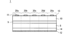
図1は、本実施の形態における半導体レーザアレイ1の斜視図である。また、図2は、本実施の形態における半導体レーザアレイ1の断面図(図1中の線分ABにおける断面図)である。図1に示すように、本実施の形態における半導体レーザアレイ1は、複数のレーザ素子(即ち、第1から第5のレーザ素子20a,20b,20c,20d,20e)を備える。第1から第5のレーザ素子は、アレイ状に配置されている。アレイ状に配置とは、隣接するレーザ素子において、レーザ素子の導波路(図示せず)が互いに並行するように配置されていることを意味する。
<
<Configuration>
FIG. 1 is a perspective view of a
第1のレーザ素子20aは、導波路の光射出面である前端面に前端面反射膜5を備える。また、第1のレーザ素子20aは、導波路を挟んで前端面と反対側の面である後端面に後端面反射膜7を備える。前端面反射膜5の発光点2からレーザ光が射出される。つまり、第1のレーザ素子20aは、導波路の両端に反射膜を有する単位共振器構造である。第2のレーザ素子20bも同様に構成される。
The
第3のレーザ素子20cは、導波路(図示せず)の光射出面である前端面に前端面反射膜6を備える。また、第3のレーザ素子20cは、導波路を挟んで前端面と反対側の面である後端面に後端面反射膜7を備える。前端面反射膜6の発光点3からレーザ光が射出される。つまり、第3のレーザ素子20cは、導波路の両端に反射膜を有する単位共振器構造である。第4のレーザ素子20dおよび第5のレーザ素子20eも同様に構成される。
The
図1に示すように、半導体レーザアレイ1は、複数の発光点2,3が一直線上に並んだ構造となる。なお、第1から第5のレーザ素子20a,20b,20c,20d,20e間には物理的な境界が存在しないため、図1および図2では、各レーザ素子に相当する領域を便宜上破線で区切って示している。
As shown in FIG. 1, the
前端面反射膜5,6および後端面反射膜7は、導波路の端面保護および反射率制御のための誘電体多層膜である。後端面反射膜7の反射率は、前端面反射膜5,6の反射率よりも大きい。なお、半導体レーザアレイにおいて、光源の高出力動作を目的として前端面反射膜と後端面反射膜とを異なる反射率とする技術は一般に知られている。
The front end
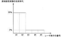
さらに、本実施の形態における半導体レーザアレイ1においては、第1、第2のレーザ素子20a,20bの前端面反射膜5と、第3から第5のレーザ素子20c,20d,20eの前端面反射膜6とで反射率が異なる。本実施の形態では、前端面反射膜5の反射率の値をR5、前端面反射膜6の反射率の値をR6とすると、R5>R6の関係が成り立つ。R5は例えば30%であり、R6は例えば3%である。
Further, in the
図3は、本実施の形態における半導体レーザアレイ1の前端面反射膜5,6の反射率分布を示す図である。図3に示すように、第1、2のレーザ素子20a,20bの前端面反射膜5の反射率を30%とし、第3から第5のレーザ素子20c,20d,20eの前端面反射膜6の反射率を3%とする。前端面反射膜5,6の反射率をこのような値とすることにより、スペックル低減効果を得ることができる。
FIG. 3 is a diagram showing the reflectance distribution of the front end
図2に示すように、半導体レーザアレイ1の各レーザ素子は、ブロードエリアレーザである。基板14(例えばGaAs基板)上には下部クラッド層8、活性層9、上部クラッド層10が順に積層されている。基板14の下面には下部電極12が設けられる。また、上部クラッド層10上面には上部電極11が設けられる。また、上部電極11の間には絶縁膜13が形成される。
As shown in FIG. 2, each laser element of the
一般的にブロードエリアレーザは、図2に示すような単純な構成をしており、上部電極11の幅に比例した高出力化が可能であることを特徴とする。なお、絶縁膜13はSiO2等で構成され、注入電流の狭窄、リーク電流の阻止、および半導体表面の保護を目的として堆積される。
In general, a broad area laser has a simple configuration as shown in FIG. 2 and is characterized in that a high output proportional to the width of the
<製造方法>
半導体レーザアレイ1の製造方法について説明する。まず、初期成長を行う基板14上に、有機金属気相成長法(MOCVD法)等により下部クラッド層8、活性層9、および上部クラッド層10を形成する。次に、第1から第5のレーザ素子20a,20b,20c,20d,20eの導波路に対応した導波路パターンを、フォトリソグラフィにより形成する。なお、導波路パターンは等間隔で形成される。また、隣接する導波路パターンは、光的な相互干渉が生じない距離を設けて形成される。そして、絶縁膜13および上部電極11を形成する。以上の工程は、ごく一般的なブロードエリアレーザの製造方法である。
<Manufacturing method>
A method for manufacturing the
次に、前端面反射膜5,6の形成方法について説明する。前端面反射膜5,6の形成は、第1蒸着工程と第2蒸着工程とからなる。まず、第1蒸着工程において、第1から第5のレーザ素子20a,20b,20c,20d,20eの前端面に対して、一様に蒸着ビーム16を照射する。第3から第5のレーザ素子20c,20d,20eの前端面反射膜6が所望の反射率(例えば3%)を得られる厚みになるまで照射を行う。この結果、各レーザ素子の前端面に均一な誘電体多層膜(反射率3%)が成膜される。図4(a)は、第1蒸着工程における半導体レーザアレイ1の上面図である。第1蒸着工程においては、均一な厚みの誘電体多層膜が成膜されるため、前端面反射膜5と前端面反射膜6の厚みは等しい。
Next, a method for forming the front end
次に、第2蒸着工程を行う。図4(b)は、第2蒸着工程における半導体レーザアレイ1の上面図である。第2蒸着工程においては、第3から第5のレーザ素子20c,20d,20eの前端面反射膜6を遮蔽マスク15で覆った状態で蒸着ビーム16の照射を行う。第1、第2のレーザ素子20a,20bの前端面反射膜5が所望の反射率(例えば30%)を得られる厚みになるまで照射を行う。第2蒸着工程において、遮蔽マスク15により蒸着ビーム16の一部が遮られているため、前端面反射膜6には誘電体多層膜が蒸着されない。
Next, a 2nd vapor deposition process is performed. FIG. 4B is a top view of the
第1、第2蒸着工程を行った結果、第1、第2のレーザ素子20a,20bの前端面反射膜5(反射率30%)と、第3から第5のレーザ素子20c,20d,20eの前端面反射膜6(反射率3%)とで、反射率に差が生じる。
As a result of performing the first and second vapor deposition steps, the front end face reflection film 5 (
なお、図4(a)および図4(b)において、蒸着ビーム16の発生源である蒸着源は図中から省いている。また、各レーザ素子の後端面には、所望の反射率(例えば95%)を得られる厚みになるまで蒸着ビームの照射を行うことにより、誘電体多層膜を均一に蒸着させて、後端面反射膜7を成膜する。
In FIG. 4A and FIG. 4B, the vapor deposition source that is the source of the
<動作>
以下では、説明のし易さのために、第1、第2のレーザ素子20a,20bを第1グループ、第3から第5のレーザ素子20c,20d,20eを第2グループとする。本実施の形態の半導体レーザアレイ1において、第1グループの半導体素子の前端面反射膜5と、第2グループの半導体素子の前端面反射膜6とで反射率を異ならせるのは、それぞれの前端面から異なる波長の光を出射させるためである。また、第1グループと、第2グループとでレーザ素子の個数が異なるのは、異なる波長光の出力を均一化するためである。これらの原理について以下で詳しく述べる。
<Operation>
In the following, for ease of explanation, the first and
上述のように、半導体レーザアレイ1は、第1グループのレーザ素子と、第2グループのレーザ素子が並列に配置された構造となっている。このため、各レーザ素子を同一条件で駆動した際に、第1、第2のグループのレーザ素子間において、発振しきい値に違いが生じる。これは、レーザのしきい値利得gth(単位[cm−1])が一般的に以下の式で表されることからわかる。
As described above, the

式(1)において、Γは導波路の光閉じ込め係数、αiは導波路損失(単位[cm−1])、Lは導波路の共振器長(単位[μm−1])、RfおよびRrはそれぞれレーザ素子の前端面反射膜5,6の反射率、後端面反射膜7の反射率である。なお、式(1)の右辺第2項は、導波路のミラー損失αm(単位[cm−1])に相当する。ここで、半導体レーザアレイ1において、各レーザ素子の導波路構造は等しいため、導波路構造に依存するパラメータである光閉じ込め係数Γ、導波路損失αi、および共振器長Lは各レーザ素子間で等しい。また、後端面反射膜7の反射率Rrも各レーザ素子間で等しい。つまり、第1、第2グループのレーザ素子間で前端面反射膜5,6の反射率Rfのみが異なる。従って、第1、第2グループ間において、レーザ素子のしきい値利得gthが異なる値となる。しきい値利得gthが異なるということは、発振しきい値電流Ith(単位[A])が異なることに等しい。
In equation (1), Γ is the optical confinement factor of the waveguide, α i is the waveguide loss (unit [cm −1 ]), L is the resonator length of the waveguide (unit [μm −1 ]), R f and R r is the reflectance of the front end
ここで、前端面反射膜5の反射率R5が前端面反射膜6の反射率R6よりも大きい(R5>R6)ことを考慮すると、式(1)より、第1グループのレーザ素子のしきい値利得gthは、第2グループのレーザ素子のしきい値利得gthよりも小さくなる。よって、第1グループのレーザ素子の発振しきい値(これをI5とする)は、第2グループのレーザ素子の発振しきい値(これをI6とする)よりも小さくなる。つまり、I5<I6の関係が成立する。 Here, considering that the reflectance R 5 of the front end surface reflecting film 5 is larger than the reflectance R 6 of the front end surface reflecting film 6 (R 5 > R 6 ), the laser of the first group is obtained from the equation (1). threshold gain g th element is smaller than the threshold gain g th of the laser element of the second group. Therefore, the oscillation threshold value of the first group of laser elements (referred to as I 5 ) is smaller than the oscillation threshold value of the second group of laser elements (referred to as I 6 ). That is, the relationship of I 5 <I 6 is established.
ここで、反射率の変化が出力効率に及ぼす影響を無視すると、第1、第2グループのレーザ素子について、電流と出力の関係は図5のように表される。 Here, when the influence of the change in reflectance on the output efficiency is ignored, the relationship between the current and the output is expressed as shown in FIG. 5 for the laser elements in the first and second groups.
なお、半導体レーザアレイ1の各レーザ素子(20a,20b,20c,20d,20e)は、同一条件で駆動される。このことは、各レーザ素子の導波路が同一構造、すなわち等しい抵抗値を有していれば、単一電源での駆動により容易に実現できる。従って、各レーザ素子の駆動条件として駆動電流Iop(単位[A])を与えると、図5に示したように、第1グループのレーザ素子の出力P5(単位[W])は、第グループのレーザ素子の出力P6よりも大きくなる(P5>P6)。
Each laser element (20a, 20b, 20c, 20d, 20e) of the
半導体レーザアレイ1における各レーザ素子の導波路における発熱量ΔT(単位[K])は以下の式(2)で表される。
The heat generation amount ΔT (unit [K]) in the waveguide of each laser element in the
![]()
![]()
ここで、Vop(単位[V])は駆動電圧、Rth(単位[K/W])は導波路の熱抵抗である。駆動条件(すなわちIopとVop)および熱抵抗Rthは、各レーザ素子間で等しいため、式(2)の右辺において前端面反射膜5,6の反射率に依存して変化するのは出力Pのみである。従って、第1、第2グループのレーザ素子間において、発熱量ΔTは出力Pに対応して異なる値となる。つまり、第1グループのレーザ素子における発熱量ΔT5は、第2グループのレーザ素子における発熱量ΔT6よりも小さくなる(ΔT5<ΔT6)。
Here, V op (unit [V]) is the driving voltage, and R th (unit [K / W]) is the thermal resistance of the waveguide. Since the driving conditions (that is, I op and V op ) and the thermal resistance R th are equal between the laser elements, the change on the right side of the equation (2) depends on the reflectance of the front end
なお、レーザ素子の発振波長は、導波路での発熱量ΔTに応じてシフトすることが知られている。シフトする波長の度合いは、一般的に、赤色で0.2nm/K、青色で0.05nm/K程度である。 It is known that the oscillation wavelength of the laser element shifts according to the heat generation amount ΔT in the waveguide. The degree of wavelength to be shifted is generally about 0.2 nm / K for red and 0.05 nm / K for blue.
つまり、半導体レーザアレイ1を構成する各レーザ素子の前端面反射膜5,6の反射率に分布を与えると、出力光の波長のシフト量に分布が生じる。よって、第1、第2グループのレーザ素子間で異なる波長のレーザ光を出力することが可能となる。第1グループのレーザ素子の波長シフト量Δλ5は、レーザ光を赤色とすると0.2×ΔT5となる。第2グループのレーザ素子の波長シフト量Δλ6は、レーザ光を赤色とすると0.2×ΔT6となる。ここで、前述のようにΔT5<ΔT6の関係があるため、Δλ5<Δλ6の関係が成り立つ。
That is, when a distribution is given to the reflectance of the front end
以上の原理により、半導体レーザアレイ1の前端面反射膜5,6の反射率を異ならせることで、半導体レーザアレイ1の出力光の波長を多重化することが可能となる。また、これによりスペックルノイズの低減が可能となる。
Based on the above principle, the wavelengths of the output light of the
なお、図2で示した出力Pの各レーザ素子間でのばらつき量(すなわち、発熱量ΔTのばらつき量)は、実際には様々な要因の影響を受ける。その主な要因としては、反射率の変化による出力効率への影響がある。 Note that the variation amount of the output P between the laser elements shown in FIG. 2 (that is, the variation amount of the heat generation amount ΔT) is actually affected by various factors. The main factor is the effect on output efficiency due to changes in reflectivity.
まず、反射率の増大により出力効率が上昇する要因として導波路損失の低減がある。これは上述したように反射率が増大すると発振しきい値が低下し、それによって導波路内に存在する自由キャリア密度の低下が生じ、結果的に光の吸収が抑制されるためである。 First, a factor that increases output efficiency due to an increase in reflectivity is a reduction in waveguide loss. This is because, as described above, when the reflectivity increases, the oscillation threshold value decreases, thereby causing a decrease in the density of free carriers existing in the waveguide, resulting in suppression of light absorption.
一方、反射率の増大により出力効率が低下する要因としては反射率増加によるミラー損失の減少がある。一般的に、レーザの光のミラー(すなわち共振端面)での損失が、出力光として共振器外部に放出される。したがって、反射率が高いということは、それだけ光が外部へ放出されにくいということを意味する。これは、出力効率が低下することに等しい。 On the other hand, a factor that decreases output efficiency due to an increase in reflectivity is a decrease in mirror loss due to an increase in reflectivity. In general, a loss of laser light in a mirror (that is, a resonance end face) is emitted to the outside of the resonator as output light. Therefore, a high reflectance means that light is less likely to be emitted to the outside. This is equivalent to a decrease in output efficiency.
以上のように、前端面反射膜5,6の反射率に応じて出力効率が変化するため、第1、第2グループのレーザ素子からの出力を、図5のように互いに平行にすることは実際上難しい。しかし、適切に駆動電流値Iopを設定することで、第1、第2グループのレーザ素子の出力にばらつきを生じさせ、第1、第2グループのレーザ素子の導波路における発熱量の差を調整することが可能である。
As described above, since the output efficiency changes according to the reflectance of the front end
図6は、レーザ素子の出力Pおよび波長シフト量Δλの、前端面反射膜5,6の反射率依存性を示す図である。図6の横軸は前端面反射膜5,6の反射率Rfを表す。図6の縦軸は、波長シフト量Δλと、出力Pをそれぞれ表す。図6において、後端面反射膜7の反射率Rrは95%で一定としている。図4は、前端面反射率Rfの変化が波長シフト量Δλおよび出力Pに及ぼす影響をあらわした一例である。
FIG. 6 is a diagram showing the dependency of the output P of the laser element and the wavelength shift amount Δλ on the reflectance of the front end
図6から、第1グループのレーザ素子の前端面反射膜5の反射率(R5)を30%とし、第2グループのレーザ素子の前端面反射膜6の反射率(R6)を3%とした場合、波長シフト量Δλの差がおよそ2nmとなることがわかる。半導体レーザアレイ1の出力光に2nmのスペクトル幅を持たせることで、十分なスペックルノイズ低減効果が期待できる。
From FIG. 6, the reflectance (R 5 ) of the front end
一方、図6に示したように、前端面反射膜5,6の反射率の変化に応じてレーザ素子の出力も大きく変動する。図4に示すように、反射率Rfの増大に伴って出力Pが増大している。
On the other hand, as shown in FIG. 6, the output of the laser element varies greatly according to the change in the reflectance of the front end
本実施の形態のように、半導体レーザアレイ1を多波長化することによりスペックルノイズを低減させる場合、異なる波長の光の出力値は近い値になることが望ましい。そこで、本実施の形態における半導体レーザアレイ1では、第1グループのレーザ素子の個数を、第2グループのレーザ素子の個数よりも少なくする。
When the speckle noise is reduced by increasing the number of wavelengths of the
つまり、本実施の形態においては、前端面反射膜5の反射率が相対的に大きい第1、第2のレーザ素子20a,20b(即ち、出力が大きいレーザ素子)の個数を、前端面反射膜6の反射率が相対的に小さい第3から第5のレーザ素子20c,20d,20e(即ち、出力が小さいレーザ素子)の個数よりも少なくする。これにより、波長の異なる2つの出力光の出力を近づけることが可能である。
That is, in the present embodiment, the number of the first and
本実施の形態の図1に示す半導体レーザアレイ1では、2つのレーザ素子(第1、第2のレーザ素子20a,20b)の前端面反射膜5に相対的に大きい反射率(例えば30%)を与え、3つのレーザ素子(第3から第5のレーザ素子20c,20d,20e)の前端面反射膜6に相対的に小さい反射率(例えば3%)を与えることで、波長の異なる出力光間で、出力の均一化を図っている。
In the
<効果>
本実施の形態における半導体レーザアレイ1は、複数のレーザ素子(即ち第1から第5のレーザ素子20a,20b,20c,20d,20e)を備える半導体レーザアレイ1であって、複数のレーザ素子は、レーザ素子の導波路が並行するように配置され、複数のレーザ素子の各々は、導波路の光射出面である前端面に前端面反射膜5,6を備え、複数のレーザ素子の各々は、前端面と導波路を挟んで反対側の面である後端面に後端面反射膜7を備え、複数のレーザ素子のうち、少なくとも2つのレーザ素子において、前端面反射膜5,6の反射率が異なり、複数のレーザ素子において、後端面反射膜7の反射率が等しく、複数のレーザ素子は単一の電源により駆動されることを特徴とする。
<Effect>
The
従って、本実施の形態における半導体レーザアレイ1によれば、複数のレーザ素子間において前端面反射膜5,6の反射率を異ならせる簡易な構成により、半導体レーザアレイを多波長化して、スペックルノイズを低減させることが可能である。前端面反射膜5,6の反射率は、容易かつ正確に調整することが可能であるため、半導体レーザアレイ1を容易に得ることが可能である。
Therefore, according to the
前端面反射膜の反射率を変化させて半導体レーザアレイを多波長化させる手法は、レーザ素子として最も簡単な構成の1つであるブロードエリアレーザに適用することが可能である。つまり、レーザ素子の構成としてブロードエリアレーザを採用することで、容易に半導体レーザアレイを多波長化することが可能である。 The technique of changing the reflectance of the front end face reflection film to increase the wavelength of the semiconductor laser array can be applied to a broad area laser which is one of the simplest configurations as a laser element. That is, by adopting a broad area laser as a configuration of the laser element, it is possible to easily increase the wavelength of the semiconductor laser array.
さらに、本実施の形態の半導体レーザアレイ1は、同一の構造を有する複数のレーザ素子の前端面反射膜5,6の反射率を異ならせることで多波長化を実現するので、多波長化のために半導体レーザの内部構造を変化させる必要がない。つまり、半導体レーザアレイ1の製造過程において特許文献1のように複数回の結晶成長を行う必要がなく、また、特許文献2のように導波路間隔を変調する必要もないため、本実施の形態の半導体レーザアレイ1は生産性に優れている。
Furthermore, since the
また、製造過程において半導体の結晶成長を複数回行う必要が無いことは、信頼性の面でも有利である。即ち、本実施の形態における半導体レーザアレイ1は、格子欠陥の少ない良質な半導体結晶からなる活性層を有するため、長時間の高出力駆動が可能となる。
In addition, the fact that there is no need to perform semiconductor crystal growth a plurality of times in the manufacturing process is advantageous in terms of reliability. That is, since the
また、本実施の形態における半導体レーザアレイ1において、複数のレーザ素子は同一構造であり、各レーザ素子の導波路は等間隔で配置される。各レーザ素子の導波路は互いに光的に干渉しない十分な距離を設けて配置することができる。従って、本実施の形態の半導体レーザアレイ1によれば、導波路の間隔の変調による多波長化手法において問題となる、隣接するレーザ素子間の光的干渉による不安定動作を回避することが可能である。
In the
また、本実施の形態の半導体レーザアレイ1は、前端面反射膜5,6の反射率の調整のみで多くの条件を設定できるため、多様な要求仕様に対応可能である。
In addition, since the
また、本実施の形態の半導体レーザアレイ1は、各レーザ素子の導波路が互いに等しい構造を有するため、各電極を同一電源に接続することで、それぞれのレーザ素子を同一の条件で駆動することが可能となる。すなわち、複雑な駆動回路を必要としないため、機構面およびコスト面で有利である。ここで、半導体レーザアレイ1が単一電源のみで駆動可能なのは、各レーザ素子の導波路が互いに等しい構造を有しており、半導体レーザアレイ1を、「各レーザ素子の導波路が互いに等しい抵抗値を備えた並列回路」とみなして駆動できるためである。
In addition, since the
本実施の形態の半導体レーザアレイ1は、単一電源で発振波長の異なる複数のレーザ素子を同時に駆動できるため、表示装置の光源としての応用上も好ましい。これは、スペックル低減を実現するにあたっては、スペクトル幅の広い光、すなわち複数波長を多重した光を同時にスクリーンへ照射する必要があるからである。
Since the
なお、半導体レーザアレイ1の各レーザ素子は、構造が単純な利得導波型(例えばブロードエリアレーザ)だけでなく、屈折率導波型(例えば、リッジ型レーザ、埋め込みヘテロレーザ)でも構成することができる。ただし、いずれの場合においても、同一基板上に等しい構造の複数のレーザ素子を形成することによって、これら複数のレーザ素子を容易に等しい条件で駆動可能となるため、本発明の効果を十分に発揮できる。
Each laser element of the
また、本実施の形態における半導体レーザアレイ1において、複数のレーザ素子(即ち第1から第5のレーザ素子20a,20b,20c,20d,20e)は、第1グループと第2グループとを含み、第1グループを構成するレーザ素子(第1、第2のレーザ素子20a,20b)の前端面反射膜5は第1の反射率(即ち反射率R5)を有し、第2グループを構成するレーザ素子(第3から第5のレーザ素子20c,20d,20e)の前端面反射膜6は第2の反射率(即ち反射率R6)を有し、第1の反射率は第2の反射率よりも大きいことを特徴とし、レーザ素子の出力が前端面反射膜5,6の反射率の増大に伴って増大する場合、第1グループを構成するレーザ素子の個数は、第2グループを構成する前記レーザ素子の個数よりも少ないことを特徴とし、レーザ素子の出力が前端面反射膜5,6の反射率の増大に伴って減少する場合、第1グループを構成するレーザ素子の個数は、第2グループを構成するレーザ素子の個数よりも多いことを特徴とする。
In the
本実施の形態では、第1グループのレーザ素子の前端面反射膜5の反射率R5が、第2グループのレーザ素子の前端面反射膜6の反射率R6よりも大きい(R5>R6)。また、本実施の形態におけるレーザ素子の出力は、図6に示すように、前端面反射膜の反射率の増大に伴って増大する。従って、相対的に出力が大きい第1グループのレーザ素子(第1、第2のレーザ素子20a,20b)の個数を、相対的に出力が小さい第2グループのレーザ素子(第3から第5のレーザ素子20c,20d,20e)の個数よりも少なくする。これにより、グループ間の出力の差を小さくすることが可能である。
In the present embodiment, the reflectance R 5 of the front end
また、本実施の形態における半導体レーザアレイ1において、複数のレーザ素子(即ち第1から第5のレーザ素子20a,20b,20c,20d,20e)は、同一基板上に形成されており、複数のレーザ素子は、前端面反射膜5,6の反射率以外の特性が同じであることを特徴とする。
In the
従って、複数のレーザ素子(即ち第1から第5のレーザ素子20a,20b,20c,20d,20e)を、同一基板上に形成することにより、一般的なレーザアレイと同様の製造方法で、レーザアレイを製造した後、前端面反射膜5,6の反射率だけを異ならせることによって、半導体レーザアレイ1を容易に得ることが可能である。
Therefore, by forming a plurality of laser elements (that is, the first to
また、本実施の形態における半導体レーザアレイ1において、複数のレーザ素子(即ち第1から第5のレーザ素子20a,20b,20c,20d,20e)はブロードエリアレーザであることを特徴とする。
In the
従って、レーザ素子を製造の容易なブロードエリアレーザとすることで、容易に半導体レーザアレイ1を得ることが可能である。
Therefore, the
<実施の形態2>
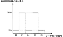
図7は、本実施の形態における半導体レーザアレイの前端面反射膜の反射率分布を示す図である。実施の形態1(図3)においては、第1、第2、第3、第4、第5のレーザ素子の順に並べて、複数のレーザ素子を配置した。一方、本実施の形態では、図7に示すように、第3、第1、第4、第2、第5のレーザ素子の順に並べて、複数のレーザ素子を配置する。つまり、前端面反射膜の反射率の異なるレーザ素子を交互に配置する。それ以外の構成は実施の形態1と同じため、説明を省略する。
<
FIG. 7 is a diagram showing the reflectance distribution of the front end face reflection film of the semiconductor laser array in the present embodiment. In the first embodiment (FIG. 3), a plurality of laser elements are arranged in the order of the first, second, third, fourth, and fifth laser elements. On the other hand, in this embodiment, as shown in FIG. 7, a plurality of laser elements are arranged in the order of the third, first, fourth, second, and fifth laser elements. That is, the laser elements having different reflectivities of the front end face reflection film are alternately arranged. Since other configurations are the same as those of the first embodiment, description thereof is omitted.
<効果>
本実施の形態における半導体レーザアレイにおいて、前端面反射膜の反射率の異なるレーザ素子が交互に配置されることを特徴とする。
<Effect>
The semiconductor laser array according to the present embodiment is characterized in that laser elements having different reflectances of the front end face reflection film are alternately arranged.
従って、前端面反射膜の反射率の異なるレーザ素子を交互に配置することにより、半導体レーザアレイ1の出力光において、波長の空間分布を均一化することが可能である。
Therefore, by alternately arranging laser elements having different reflectivities of the front end face reflection film, it is possible to make the spatial distribution of wavelengths uniform in the output light of the
<実施の形態3>
図8は、本実施の形態における半導体レーザアレイの前端面反射膜の反射率分布を示す図である。本実施の形態において、半導体レーザアレイは第1から第6のレーザ素子を備える。第1から第6のレーザ素子は、実施の形態1と同様、レーザ素子の導波路が並行するように配置されている。
<
FIG. 8 is a diagram showing the reflectance distribution of the front end face reflection film of the semiconductor laser array in the present embodiment. In the present embodiment, the semiconductor laser array includes first to sixth laser elements. As in the first embodiment, the first to sixth laser elements are arranged so that the waveguides of the laser elements are parallel to each other.
本実施の形態において、第1のレーザ素子の前端面反射膜は反射率R1を有する。第2、第3のレーザ素子の前端面反射膜は反射率R2を有する。第4から第6のレーザ素子の前端面反射膜は反射率R3を有する。ここで、R1>R2>R3の関係であるとする。それ以外の構成は実施の形態1と同じため、説明を省略する。 In this embodiment, the front facet reflection film of the first laser element has a reflectivity R 1. The second, front end face reflection film of the third laser element having a reflectivity R 2. Front facet reflection film of the sixth laser element from the fourth has a reflectivity R 3. Here, it is assumed that the relation of R 1 > R 2 > R 3 is satisfied. Since other configurations are the same as those of the first embodiment, description thereof is omitted.
このように、複数のレーザ素子において前端面反射膜の反射率を3種類にすることで、3つの異なる波長を重畳して半導体レーザアレイを多波長化することができる。よって、実施の形態1と比較して、出力光のスペクトル幅をさらに拡大することが可能なため、スペックルの低減効果をさらに向上させることが可能である。
Thus, by using three types of reflectance of the front end face reflection film in the plurality of laser elements, the semiconductor laser array can be multi-wavelength by superimposing three different wavelengths. Therefore, compared with
なお、本発明は、その発明の範囲内において、各実施の形態を自由に組み合わせたり、各実施の形態を適宜、変形、省略することが可能である。 It should be noted that the present invention can be freely combined with each other within the scope of the invention, and each embodiment can be appropriately modified or omitted.
1 半導体レーザアレイ、2,3 発光点、5,6 前端面反射膜、7 後端面反射膜、8 下部クラッド層、9 活性層、10 上部クラッド層、11 上部電極、12 下部電極、13 絶縁膜、14 基板、15 遮蔽マスク、16 蒸着ビーム、20a 第1のレーザ素子、20b 第2のレーザ素子、20c 第3のレーザ素子、20d 第4のレーザ素子、20e 第5のレーザ素子。
DESCRIPTION OF
Claims (5)
前記複数のレーザ素子は、前記レーザ素子の導波路が並行するように配置され、
前記複数のレーザ素子の各々は、前記導波路の光射出面である前端面に前端面反射膜を備え、
前記複数のレーザ素子の各々は、前記前端面と前記導波路を挟んで反対側の面である後端面に後端面反射膜を備え、
前記複数のレーザ素子のうち、少なくとも2つの前記レーザ素子において、前記前端面反射膜の反射率が異なり、
前記複数のレーザ素子において、前記後端面反射膜の反射率が等しく、
前記複数のレーザ素子は単一の電源により駆動されることを特徴とする、
半導体レーザアレイ。 A semiconductor laser array comprising a plurality of laser elements,
The plurality of laser elements are arranged so that the waveguides of the laser elements are parallel to each other,
Each of the plurality of laser elements includes a front end surface reflecting film on a front end surface which is a light exit surface of the waveguide,
Each of the plurality of laser elements includes a rear end surface reflection film on a rear end surface that is an opposite surface across the front end surface and the waveguide,
Among the plurality of laser elements, in at least two of the laser elements, the reflectance of the front end surface reflection film is different,
In the plurality of laser elements, the reflectance of the rear end face reflection film is equal,
The plurality of laser elements are driven by a single power source,
Semiconductor laser array.
第1グループと第2グループとを含み、
前記第1グループを構成する前記レーザ素子の前記前端面反射膜は第1の反射率を有し、
前記第2グループを構成する前記レーザ素子の前記前端面反射膜は第2の反射率を有し、
前記第1の反射率は前記第2の反射率よりも大きいことを特徴とし、
前記レーザ素子の出力が前記前端面反射膜の反射率の増大に伴って増大する場合、前記第1グループを構成する前記レーザ素子の個数は、前記第2グループを構成する前記レーザ素子の個数よりも少ないことを特徴とし、
前記レーザ素子の出力が前記前端面反射膜の反射率の増大に伴って減少する場合、前記第1グループを構成する前記レーザ素子の個数は、前記第2グループを構成する前記レーザ素子の個数よりも多いことを特徴とする、
請求項1に記載の半導体レーザアレイ。 The plurality of laser elements are:
Including a first group and a second group,
The front end face reflection film of the laser element constituting the first group has a first reflectance,
The front end face reflection film of the laser element constituting the second group has a second reflectance;
The first reflectance is larger than the second reflectance,
When the output of the laser element increases as the reflectance of the front end face reflection film increases, the number of the laser elements constituting the first group is greater than the number of the laser elements constituting the second group. Is also characterized by
When the output of the laser element decreases as the reflectance of the front end face reflection film increases, the number of the laser elements constituting the first group is greater than the number of the laser elements constituting the second group. It is also characterized by many
The semiconductor laser array according to claim 1.
前記複数のレーザ素子は、前記前端面反射膜の反射率以外の特性が同じであることを特徴とする、
請求項1または請求項2に記載の半導体レーザアレイ。 The plurality of laser elements are formed on the same substrate,
The plurality of laser elements have the same characteristics other than the reflectance of the front end face reflection film,
The semiconductor laser array according to claim 1 or 2.
請求項1から請求項3のいずれか一項に記載の半導体レーザアレイ。 The plurality of laser elements are broad area lasers,
The semiconductor laser array according to any one of claims 1 to 3.
請求項1から請求項4のいずれか一項に記載の半導体レーザアレイ。 The laser elements having different reflectivities of the front end face reflection film are alternately arranged,
The semiconductor laser array according to any one of claims 1 to 4.
Priority Applications (5)
| Application Number | Priority Date | Filing Date | Title |
|---|---|---|---|
| JP2014019166A JP6257361B2 (en) | 2014-02-04 | 2014-02-04 | Semiconductor laser array |
| US14/562,163 US9466946B2 (en) | 2014-02-04 | 2014-12-05 | Semiconductor laser array |
| CA2875175A CA2875175C (en) | 2014-02-04 | 2014-12-15 | Semiconductor laser array |
| EP15151326.4A EP2928032B1 (en) | 2014-02-04 | 2015-01-15 | Semiconductor laser array with reduced speckle noise |
| CN201510019571.4A CN104821487B (en) | 2014-02-04 | 2015-01-15 | Semiconductor laser array |
Applications Claiming Priority (1)
| Application Number | Priority Date | Filing Date | Title |
|---|---|---|---|
| JP2014019166A JP6257361B2 (en) | 2014-02-04 | 2014-02-04 | Semiconductor laser array |
Publications (2)
| Publication Number | Publication Date |
|---|---|
| JP2015146403A true JP2015146403A (en) | 2015-08-13 |
| JP6257361B2 JP6257361B2 (en) | 2018-01-10 |
Family
ID=52339079
Family Applications (1)
| Application Number | Title | Priority Date | Filing Date |
|---|---|---|---|
| JP2014019166A Expired - Fee Related JP6257361B2 (en) | 2014-02-04 | 2014-02-04 | Semiconductor laser array |
Country Status (5)
| Country | Link |
|---|---|
| US (1) | US9466946B2 (en) |
| EP (1) | EP2928032B1 (en) |
| JP (1) | JP6257361B2 (en) |
| CN (1) | CN104821487B (en) |
| CA (1) | CA2875175C (en) |
Cited By (1)
| Publication number | Priority date | Publication date | Assignee | Title |
|---|---|---|---|---|
| JP7371522B2 (en) | 2020-02-19 | 2023-10-31 | ウシオ電機株式会社 | semiconductor laser equipment |
Families Citing this family (10)
| Publication number | Priority date | Publication date | Assignee | Title |
|---|---|---|---|---|
| US9800017B1 (en) | 2009-05-29 | 2017-10-24 | Soraa Laser Diode, Inc. | Laser device and method for a vehicle |
| US10938182B2 (en) | 2015-08-19 | 2021-03-02 | Soraa Laser Diode, Inc. | Specialized integrated light source using a laser diode |
| US10879673B2 (en) | 2015-08-19 | 2020-12-29 | Soraa Laser Diode, Inc. | Integrated white light source using a laser diode and a phosphor in a surface mount device package |
| US11437774B2 (en) | 2015-08-19 | 2022-09-06 | Kyocera Sld Laser, Inc. | High-luminous flux laser-based white light source |
| JP6572803B2 (en) * | 2016-03-09 | 2019-09-11 | 三菱電機株式会社 | Semiconductor laser device |
| US11421843B2 (en) * | 2018-12-21 | 2022-08-23 | Kyocera Sld Laser, Inc. | Fiber-delivered laser-induced dynamic light system |
| US11239637B2 (en) | 2018-12-21 | 2022-02-01 | Kyocera Sld Laser, Inc. | Fiber delivered laser induced white light system |
| US20220037851A1 (en) * | 2019-01-10 | 2022-02-03 | Mitsubishi Electric Corporation | Semiconductor laser device |
| US11884202B2 (en) | 2019-01-18 | 2024-01-30 | Kyocera Sld Laser, Inc. | Laser-based fiber-coupled white light system |
| CN109921283B (en) * | 2019-02-01 | 2020-11-10 | 苏州长光华芯光电技术有限公司 | Semiconductor device and preparation method |
Citations (10)
| Publication number | Priority date | Publication date | Assignee | Title |
|---|---|---|---|---|
| JPS62234388A (en) * | 1986-04-04 | 1987-10-14 | Matsushita Electric Ind Co Ltd | Semiconductor laser array device |
| JPS63272089A (en) * | 1987-04-30 | 1988-11-09 | Oki Electric Ind Co Ltd | Semiconductor laser array |
| JPH02111091A (en) * | 1988-10-20 | 1990-04-24 | Canon Inc | Multiple-wavelength semiconductor laser |
| JPH0376189A (en) * | 1989-08-17 | 1991-04-02 | Mitsubishi Electric Corp | Coating of end face section |
| JPH05102613A (en) * | 1991-10-09 | 1993-04-23 | Fuji Xerox Co Ltd | Multiple wave length semiconductor laser device |
| JP2004503923A (en) * | 2000-07-10 | 2004-02-05 | コーポレーション フォー レーザー オプティックス リサーチ | System and method for speckle reduction by bandwidth enhancement |
| JP2007214300A (en) * | 2006-02-09 | 2007-08-23 | Sony Corp | Semiconductor laser |
| JP2008004743A (en) * | 2006-06-22 | 2008-01-10 | Sony Corp | Semiconductor laser array and optical apparatus |
| JP2009152277A (en) * | 2007-12-19 | 2009-07-09 | Sony Corp | Semiconductor laser array, light emitting device, display, processing device, and driving method |
| US20120314398A1 (en) * | 2011-04-04 | 2012-12-13 | Soraa, Inc. | Laser package having multiple emitters with color wheel |
Family Cites Families (10)
| Publication number | Priority date | Publication date | Assignee | Title |
|---|---|---|---|---|
| JPS61116891A (en) | 1984-11-13 | 1986-06-04 | Nec Corp | Semiconductor laser array device |
| US5228050A (en) * | 1992-02-03 | 1993-07-13 | Gte Laboratories Incorporated | Integrated multiple-wavelength laser array |
| JPH10117040A (en) * | 1996-10-08 | 1998-05-06 | Nec Corp | Semiconductor laser element and manufacture of the same |
| JP4462657B2 (en) * | 1998-06-04 | 2010-05-12 | ソニー株式会社 | Semiconductor light emitting device and manufacturing method thereof |
| JP2000011417A (en) | 1998-06-26 | 2000-01-14 | Toshiba Corp | Semiconductor laser array and its production, optical integrated unit, optical pickup as well as optical disk drive assembly |
| JP2004304111A (en) * | 2003-04-01 | 2004-10-28 | Sharp Corp | Multi-wavelength laser device |
| JP2005191094A (en) * | 2003-12-24 | 2005-07-14 | Hamamatsu Photonics Kk | Semiconductor laser |
| US7116690B2 (en) * | 2004-05-17 | 2006-10-03 | Textron Systems Corporation | Staggered array coupler |
| JP2009088207A (en) * | 2007-09-28 | 2009-04-23 | Panasonic Corp | Semiconductor laser device, and method for manufacturing the same |
| JP2010219436A (en) | 2009-03-18 | 2010-09-30 | Sony Corp | Multi-wavelength semiconductor laser and optical recording and reproducing device |
-
2014
- 2014-02-04 JP JP2014019166A patent/JP6257361B2/en not_active Expired - Fee Related
- 2014-12-05 US US14/562,163 patent/US9466946B2/en active Active
- 2014-12-15 CA CA2875175A patent/CA2875175C/en not_active Expired - Fee Related
-
2015
- 2015-01-15 CN CN201510019571.4A patent/CN104821487B/en not_active Expired - Fee Related
- 2015-01-15 EP EP15151326.4A patent/EP2928032B1/en active Active
Patent Citations (10)
| Publication number | Priority date | Publication date | Assignee | Title |
|---|---|---|---|---|
| JPS62234388A (en) * | 1986-04-04 | 1987-10-14 | Matsushita Electric Ind Co Ltd | Semiconductor laser array device |
| JPS63272089A (en) * | 1987-04-30 | 1988-11-09 | Oki Electric Ind Co Ltd | Semiconductor laser array |
| JPH02111091A (en) * | 1988-10-20 | 1990-04-24 | Canon Inc | Multiple-wavelength semiconductor laser |
| JPH0376189A (en) * | 1989-08-17 | 1991-04-02 | Mitsubishi Electric Corp | Coating of end face section |
| JPH05102613A (en) * | 1991-10-09 | 1993-04-23 | Fuji Xerox Co Ltd | Multiple wave length semiconductor laser device |
| JP2004503923A (en) * | 2000-07-10 | 2004-02-05 | コーポレーション フォー レーザー オプティックス リサーチ | System and method for speckle reduction by bandwidth enhancement |
| JP2007214300A (en) * | 2006-02-09 | 2007-08-23 | Sony Corp | Semiconductor laser |
| JP2008004743A (en) * | 2006-06-22 | 2008-01-10 | Sony Corp | Semiconductor laser array and optical apparatus |
| JP2009152277A (en) * | 2007-12-19 | 2009-07-09 | Sony Corp | Semiconductor laser array, light emitting device, display, processing device, and driving method |
| US20120314398A1 (en) * | 2011-04-04 | 2012-12-13 | Soraa, Inc. | Laser package having multiple emitters with color wheel |
Cited By (1)
| Publication number | Priority date | Publication date | Assignee | Title |
|---|---|---|---|---|
| JP7371522B2 (en) | 2020-02-19 | 2023-10-31 | ウシオ電機株式会社 | semiconductor laser equipment |
Also Published As
| Publication number | Publication date |
|---|---|
| CN104821487B (en) | 2017-12-12 |
| US20150222091A1 (en) | 2015-08-06 |
| CN104821487A (en) | 2015-08-05 |
| EP2928032B1 (en) | 2019-10-02 |
| CA2875175A1 (en) | 2015-08-04 |
| US9466946B2 (en) | 2016-10-11 |
| CA2875175C (en) | 2017-12-05 |
| JP6257361B2 (en) | 2018-01-10 |
| EP2928032A1 (en) | 2015-10-07 |
Similar Documents
| Publication | Publication Date | Title |
|---|---|---|
| JP6257361B2 (en) | Semiconductor laser array | |
| JP5187474B2 (en) | Semiconductor laser array and optical apparatus | |
| US7772606B2 (en) | Light-emitting photonic device | |
| US7620091B2 (en) | Broadband laser lamp with reduced speckle | |
| JP6103202B2 (en) | Semiconductor light emitting device, superluminescent diode, and projector | |
| JP2007214300A (en) | Semiconductor laser | |
| JPWO2019021802A1 (en) | Semiconductor laser device and semiconductor laser device | |
| JP2009152277A (en) | Semiconductor laser array, light emitting device, display, processing device, and driving method | |
| JP6040790B2 (en) | Light emitting device, super luminescent diode, and projector | |
| US9423678B2 (en) | Light emitting device, and super luminescent diode | |
| US20120235196A1 (en) | Light emitting device and projector | |
| TW201635586A (en) | Light emitting device and projector | |
| KR20080024719A (en) | Vertical cavity surface emitting laser | |
| JP2001077426A (en) | Semiconductor light-emitting device | |
| US7672353B2 (en) | Semiconductor laser device and method for its production | |
| JP2010165704A (en) | Semiconductor laser and method of manufacturing the same | |
| JP6895903B2 (en) | Semiconductor laser device, diffraction grating structure, and diffraction grating | |
| JP6512953B2 (en) | Semiconductor laser device | |
| JP4292786B2 (en) | Semiconductor laser device | |
| US20150062541A1 (en) | Light emitting device and projector | |
| US8139618B2 (en) | Light emission device, light emission device driving method, and projector | |
| WO2018008381A1 (en) | Optical element, active layer structure, and display device | |
| JPH11307874A (en) | Optical isolator, distributed feedback laser and optical integrated element | |
| JP2022188835A (en) | Semiconductor laser device | |
| JP2000022265A (en) | Semiconductor laser |
Legal Events
| Date | Code | Title | Description |
|---|---|---|---|
| A621 | Written request for application examination |
Free format text: JAPANESE INTERMEDIATE CODE: A621 Effective date: 20161202 |
|
| A977 | Report on retrieval |
Free format text: JAPANESE INTERMEDIATE CODE: A971007 Effective date: 20170816 |
|
| A131 | Notification of reasons for refusal |
Free format text: JAPANESE INTERMEDIATE CODE: A131 Effective date: 20170822 |
|
| A521 | Request for written amendment filed |
Free format text: JAPANESE INTERMEDIATE CODE: A523 Effective date: 20171020 |
|
| TRDD | Decision of grant or rejection written | ||
| A01 | Written decision to grant a patent or to grant a registration (utility model) |
Free format text: JAPANESE INTERMEDIATE CODE: A01 Effective date: 20171107 |
|
| A61 | First payment of annual fees (during grant procedure) |
Free format text: JAPANESE INTERMEDIATE CODE: A61 Effective date: 20171205 |
|
| R150 | Certificate of patent or registration of utility model |
Ref document number: 6257361 Country of ref document: JP Free format text: JAPANESE INTERMEDIATE CODE: R150 |
|
| R250 | Receipt of annual fees |
Free format text: JAPANESE INTERMEDIATE CODE: R250 |
|
| LAPS | Cancellation because of no payment of annual fees |