JP2015114453A - Electrophotographic photoreceptor and method for manufacturing the same, and image forming apparatus - Google Patents
Electrophotographic photoreceptor and method for manufacturing the same, and image forming apparatus Download PDFInfo
- Publication number
- JP2015114453A JP2015114453A JP2013255808A JP2013255808A JP2015114453A JP 2015114453 A JP2015114453 A JP 2015114453A JP 2013255808 A JP2013255808 A JP 2013255808A JP 2013255808 A JP2013255808 A JP 2013255808A JP 2015114453 A JP2015114453 A JP 2015114453A
- Authority
- JP
- Japan
- Prior art keywords
- fine particles
- photosensitive member
- layer
- electrophotographic photosensitive
- coating
- Prior art date
- Legal status (The legal status is an assumption and is not a legal conclusion. Google has not performed a legal analysis and makes no representation as to the accuracy of the status listed.)
- Granted
Links
Images

Landscapes
- Photoreceptors In Electrophotography (AREA)
Abstract
Description
本発明は、電子写真感光体およびその製造方法、並びに当該電子写真感光体を備える画像形成装置に関する。 The present invention relates to an electrophotographic photosensitive member, a method for producing the same, and an image forming apparatus including the electrophotographic photosensitive member.
従来、電子写真方式の画像形成装置において用いられる電子写真感光体(以下、単に「感光体」ともいう。)としては、無機感光体および有機感光体が知られている。
ここにいう「電子写真方式」とは一般に、光導電性の感光体をまず暗所で、例えばコロナ放電によって帯電させ、次いで露光し、露光部のみの電荷を選択的に逸散させて静電潜像を得て、この潜像部を染料、顔料などの着色剤および樹脂材料などで構成されるトナーで現像し、可視化して画像を形成する画像形成プロセスである。
Conventionally, an inorganic photoreceptor and an organic photoreceptor are known as an electrophotographic photoreceptor (hereinafter also simply referred to as “photoreceptor”) used in an electrophotographic image forming apparatus.
The “electrophotographic method” here generally means that a photoconductive photoreceptor is first charged in a dark place by, for example, corona discharge, and then exposed to selectively dissipate the charge only in the exposed portion, thereby electrostatically charging. This is an image forming process in which a latent image is obtained, and this latent image portion is developed with a toner composed of a colorant such as a dye and a pigment, and a resin material, and visualized to form an image.
有機感光体は、無機感光体に比べ、感光波長域の自由度、成膜性、可撓性、膜の透明性、量産性、毒性やコスト面などにおいて利点を有するため、現在ではほとんどの感光体には有機感光体が用いられている。 Compared to inorganic photoreceptors, organic photoreceptors have advantages in terms of freedom of photosensitive wavelength range, film formability, flexibility, film transparency, mass productivity, toxicity, cost, etc. An organic photoreceptor is used for the body.
近年、感光体には、良好なクリーニング性と高い耐久性が求められている。
高い耐久性を得るため、感光体の表面層に金属酸化物微粒子を添加することが知られている。特に、低抵抗で比較的大きな粒径(特に100nm以上)を有する金属酸化物微粒子を用いることで、高耐久性と電位安定性との両立を図ることができる。
In recent years, photoreceptors are required to have good cleaning properties and high durability.
In order to obtain high durability, it is known to add metal oxide fine particles to the surface layer of the photoreceptor. In particular, by using metal oxide fine particles having a low resistance and a relatively large particle size (in particular, 100 nm or more), both high durability and potential stability can be achieved.
一方、クリーニング性向上のため、感光体の表面層に有機フィラーを添加することが知られている。有機フィラーを添加することにより、感光体表面が適度に粗面化されるため、クリーニング性の向上を図ることができる。
特許文献1では、感光体の表面層にベンゾグアナミン−メラミン−ホルムアルデヒド縮合物を添加することが開示されている。また、特許文献2では、感光体の表面層にベンゾグアナミン樹脂微粒子やメラミン樹脂微粒子を添加することが開示されている。
このようなベンゾグアナミン−メラミン−ホルムアルデヒド縮合物などの有機フィラーはトナーに対する付着力が小さいため、クリーニング性向上の効果が特に高い。しかしながら、このような有機フィラーを、金属酸化物微粒子と共に用いる場合には、表面層を形成するための塗布液において凝集が発生する。特に、大きな粒径を有する金属酸化物微粒子と共に用いると、凝集が発生しやすくなる。塗布液中の凝集物は、形成された感光体においても残留し、所期の効果を期待することができない。また、表面層中に凝集物が存在するために、クリーニングブレードの異常摩耗が発生し、クリーニング性を著しく低下させることとなる。
On the other hand, it is known to add an organic filler to the surface layer of the photoreceptor in order to improve cleaning properties. By adding the organic filler, the surface of the photoreceptor is appropriately roughened, and thus the cleaning property can be improved.
Such an organic filler such as a benzoguanamine-melamine-formaldehyde condensate has a particularly low effect of improving the cleaning property because of its low adhesion to the toner. However, when such an organic filler is used together with metal oxide fine particles, aggregation occurs in the coating liquid for forming the surface layer. In particular, when used together with metal oxide fine particles having a large particle size, aggregation tends to occur. Aggregates in the coating solution remain in the formed photoreceptor, and the expected effect cannot be expected. In addition, the presence of aggregates in the surface layer causes abnormal wear of the cleaning blade, which significantly reduces the cleaning performance.
本発明は、以上のような事情を考慮してなされたものであって、その目的は、良好なクリーニング性を有すると共に、高い耐久性を有する電子写真感光体およびその製造方法を提供することにある。また、本発明の他の目的は、長期間にわたって高画質な画像を形成することができる画像形成装置を提供することにある。 The present invention has been made in view of the above circumstances, and an object thereof is to provide an electrophotographic photosensitive member having good cleaning properties and high durability and a method for producing the same. is there. Another object of the present invention is to provide an image forming apparatus capable of forming a high-quality image over a long period of time.
本発明の電子写真感光体は、導電性支持体上に感光層が形成され、この感光層上に表面層が形成されてなる電子写真感光体において、
前記表面層は、2個以上のラジカル重合性官能基を有する化合物を重合反応することによって得られる硬化樹脂中に、少なくとも表面の一部が金属酸化物によって形成された無機微粒子、および、メラミンおよびベンゾグアナミンのうち少なくとも一種に由来の構成単位を含む樹脂からなる有機樹脂微粒子が含有されてなるものであり、
前記有機樹脂微粒子がカップリング剤によって表面処理が施されたものであることを特徴とする。
In the electrophotographic photosensitive member of the present invention, a photosensitive layer is formed on a conductive support, and a surface layer is formed on the photosensitive layer.
The surface layer includes inorganic fine particles in which at least a part of the surface is formed of a metal oxide in a cured resin obtained by polymerizing a compound having two or more radical polymerizable functional groups, and melamine and Organic resin fine particles made of a resin containing a structural unit derived from at least one of benzoguanamine are contained,
The organic resin fine particles are subjected to surface treatment with a coupling agent.
本発明の電子写真感光体においては、前記有機樹脂微粒子の数平均一次粒径が100nm以上1500nm以下であることが好ましい。 In the electrophotographic photosensitive member of the present invention, the organic resin fine particles preferably have a number average primary particle size of 100 nm to 1500 nm.
本発明の電子写真感光体においては、前記カップリング剤が、少なくともフッ素元素を含むものであることが好ましい。 In the electrophotographic photosensitive member of the present invention, the coupling agent preferably contains at least a fluorine element.
本発明の電子写真感光体においては、前記無機微粒子の数平均一次粒径が10nm以上300nm以下であることが好ましい。 In the electrophotographic photosensitive member of the present invention, the number average primary particle size of the inorganic fine particles is preferably 10 nm or more and 300 nm or less.
本発明の電子写真感光体においては、前記無機微粒子が、酸化スズおよび酸化チタンのうち少なくとも1種からなることが好ましい。 In the electrophotographic photoreceptor of the present invention, the inorganic fine particles are preferably composed of at least one of tin oxide and titanium oxide.
本発明の電子写真感光体においては、前記無機微粒子が、芯材表面に金属酸化物が被覆材として付着されてなる複合微粒子であることが好ましい。
また、前記複合微粒子において、前記芯材が、酸化アルミニウム、硫酸バリウムおよび酸化ケイ素のうち少なくとも1種からなることが好ましい。
さらに、前記複合微粒子において、前記被覆材が、酸化スズおよび酸化チタンのうち少なくとも1種からなることが好ましい。
In the electrophotographic photoreceptor of the present invention, the inorganic fine particles are preferably composite fine particles in which a metal oxide is attached to the surface of the core material as a coating material.
In the composite fine particle, the core material is preferably made of at least one of aluminum oxide, barium sulfate, and silicon oxide.
Furthermore, in the composite fine particle, the coating material is preferably made of at least one of tin oxide and titanium oxide.
本発明の電子写真感光体においては、前記ラジカル重合性官能基がアクリロイル基またはメタクリロイル基であることが好ましい。 In the electrophotographic photoreceptor of the present invention, the radical polymerizable functional group is preferably an acryloyl group or a methacryloyl group.
本発明の電子写真感光体の製造方法は、導電性支持体上に感光層が形成され、この感光層上に表面層が形成されてなる電子写真感光体の製造方法において、
感光層上に、2個以上のラジカル重合性官能基を有する化合物と、少なくとも表面の一部が金属酸化物によって形成された無機微粒子と、カップリング剤によって表面処理が施された、メラミンおよびベンゾグアナミンのうち少なくとも一種に由来の構成単位を含む樹脂からなる有機樹脂微粒子とを含有する表面層形成用塗布液を塗布して塗布膜を形成し、当該塗布膜を硬化処理する工程を有することを特徴とする。
In the method for producing an electrophotographic photosensitive member of the present invention, a photosensitive layer is formed on a conductive support, and a surface layer is formed on the photosensitive layer.
Melamine and benzoguanamine, wherein the photosensitive layer has a compound having two or more radically polymerizable functional groups, inorganic fine particles having at least part of the surface formed of a metal oxide, and a surface treatment with a coupling agent. A coating layer is formed by applying a coating solution for forming a surface layer containing organic resin fine particles composed of a resin containing a structural unit derived from at least one of the above, and the coating film is cured. And
本発明の画像形成装置は、電子写真感光体と、前記電子写真感光体の表面を帯電させる帯電手段と、当該電子写真感光体の表面に静電潜像を形成する露光手段と、前記静電潜像を、トナーを含む現像剤により現像してトナー像を形成する現像手段と、前記トナー像を転写材に転写する転写手段と、前記転写材に転写されたトナー像を定着させる定着手段と、電子写真感光体上の残留トナーを除去するクリーニング手段とを備え、
前記クリーニング手段がブレードよりなり、
前記電子写真感光体が上記の電子写真感光体であることを特徴とする。
The image forming apparatus of the present invention includes an electrophotographic photosensitive member, a charging unit that charges the surface of the electrophotographic photosensitive member, an exposure unit that forms an electrostatic latent image on the surface of the electrophotographic photosensitive member, and the electrostatic unit. Developing means for developing a latent image with a developer containing toner to form a toner image, transfer means for transferring the toner image to a transfer material, and fixing means for fixing the toner image transferred to the transfer material; Cleaning means for removing residual toner on the electrophotographic photosensitive member,
The cleaning means comprises a blade;
The electrophotographic photosensitive member is the above-described electrophotographic photosensitive member.
本発明の電子写真感光体によれば、表面層を構成する硬化樹脂中に、少なくとも表面の一部が金属酸化物によって形成された無機微粒子、および、メラミンおよびベンゾグアナミンのうち少なくとも一種に由来の構成単位を含む樹脂からなる有機樹脂微粒子が含有されてなり、この有機樹脂微粒子がカップリング剤によって表面処理が施されたものであることにより、良好なクリーニング性を有すると共に、高い耐久性が得られる。 According to the electrophotographic photoreceptor of the present invention, in the cured resin constituting the surface layer, inorganic fine particles in which at least a part of the surface is formed of a metal oxide, and a configuration derived from at least one of melamine and benzoguanamine Organic resin fine particles made of a resin containing a unit are contained, and the organic resin fine particles are subjected to surface treatment with a coupling agent, thereby providing good cleaning properties and high durability. .
本発明の電子写真感光体の製造方法によれば、表面層形成用塗布液中において有機樹脂微粒子と無機微粒子との凝集が抑制されるので、上記感光体を確実に製造することができる。 According to the method for producing an electrophotographic photosensitive member of the present invention, the aggregation of organic resin fine particles and inorganic fine particles is suppressed in the surface layer forming coating solution, so that the photosensitive member can be produced reliably.
本発明の画像形成装置によれば、上記電子写真感光体を備えることにより、長期間にわたって高画質な画像を形成することができる。 According to the image forming apparatus of the present invention, a high-quality image can be formed over a long period of time by including the electrophotographic photosensitive member.
以下、本発明について詳細に説明する。 Hereinafter, the present invention will be described in detail.
〔電子写真感光体〕
本発明の感光体の層構成は、導電性支持体上に、感光層が形成され、この感光層上に表面層が形成されてなるものであれば特に限定されないが、具体的には下記(1)および(2)に示すように、感光層および表面層がこの順に積層されてなる層構成が挙げられる。
(1)導電性支持体上に、中間層、感光層として電荷発生層および電荷輸送層、並びに表面層がこの順に積層されてなる層構成。
(2)導電性支持体上に、中間層、感光層として電荷発生物質および電荷輸送物質を含む単層、並びに表面層がこの順に積層されてなる層構成。
[Electrophotographic photoconductor]
The layer structure of the photoreceptor of the present invention is not particularly limited as long as a photosensitive layer is formed on a conductive support and a surface layer is formed on this photosensitive layer. As shown in 1) and (2), there is a layer structure in which a photosensitive layer and a surface layer are laminated in this order.
(1) A layer structure in which a charge generation layer, a charge transport layer, and a surface layer are laminated in this order as an intermediate layer and a photosensitive layer on a conductive support.
(2) A layer structure in which an intermediate layer, a single layer containing a charge generation material and a charge transport material as a photosensitive layer, and a surface layer are laminated in this order on a conductive support.
本発明の感光体は、有機感光体であり、有機感光体とは電子写真感光体の構成に必要不可欠な電荷発生機能および電荷輸送機能の少なくとも一方の機能が有機化合物によって発現される電子写真感光体を意味し、公知の有機電荷発生物質または有機電荷輸送物質から構成された感光体、電荷発生機能と電荷輸送機能とを高分子錯体で構成した感光体などを含むものとする。 The photoconductor of the present invention is an organic photoconductor, and an electrophotographic photoconductor in which at least one of a charge generation function and a charge transport function essential to the configuration of an electrophotographic photoconductor is expressed by an organic compound. And a photoreceptor composed of a known organic charge generation material or organic charge transport material, a photoreceptor composed of a polymer complex with a charge generation function and a charge transport function, and the like.
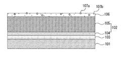
図1は、本発明の感光体における層構成の一例を示す説明用断面図である。具体的には、上記(1)の層構成を示す。この感光体は、導電性支持体101上に、感光層102が中間層103を介して積層され、この感光層102上に、表面層106が積層されている。感光層102は、中間層103上に積層される電荷発生層104と、この電荷発生層104上に積層される電荷輸送層105とにより構成される。表面層106中には有機樹脂微粒子107aと無機微粒子107bとが含有されている。
FIG. 1 is an explanatory cross-sectional view showing an example of the layer structure of the photoreceptor of the present invention. Specifically, the layer configuration of (1) above is shown. In this photoreceptor, a
〔表面層106〕
本発明の感光体を構成する表面層は、2個以上のラジカル重合性官能基を有する化合物を重合反応することによって得られる硬化樹脂中に、少なくとも表面の一部が金属酸化物によって形成された無機微粒子、および、メラミンおよびベンゾグアナミンのうち少なくとも一種に由来の構成単位を含む樹脂からなる有機樹脂微粒子が含有されてなるものである。そして、当該有機樹脂微粒子は、カップリング剤によって表面処理が施されたものである。
本発明の感光体においては、表面層が硬化樹脂により構成されていることにより、基本的に高い膜強度が得られ、また、当該硬化樹脂中に無機微粒子が含有されていることにより、より一層高い膜強度が得られる。従って、高い耐久性が得られる。さらに、有機樹脂微粒子がカップリング剤によって表面処理が施されたものであることにより、当該感光体の製造工程において調製される表面層形成用塗布液中において、当該有機樹脂微粒子と無機微粒子との凝集が抑制される。そして、この表面層形成用塗布液が感光層上に塗布され、硬化処理することによって形成された表面層においては、有機樹脂微粒子と無機微粒子との凝集物が低減される。従って、有機樹脂微粒子の特性が有効に発揮される。以上のことから、本発明の感光体によれば、良好なクリーニング性を有すると共に、高い耐久性が得られる。
ここで、無機微粒子をカップリング剤によって表面処理することによっても、有機樹脂微粒子と無機微粒子との凝集を抑制することができると考えられるが、無機微粒子が表面処理されたものであると感光体の電気特性が低下するおそれがある。そのため、本発明のように、有機樹脂微粒子がカップリング剤によって表面処理されたものであることにより、表面層中の凝集物を低減しながらも感光体としての機能を担保することができる。
[Surface layer 106]
The surface layer constituting the photoreceptor of the present invention was formed at least partially on the surface of a cured resin obtained by polymerization reaction of a compound having two or more radical polymerizable functional groups. Inorganic fine particles and organic resin fine particles made of a resin containing a structural unit derived from at least one of melamine and benzoguanamine are contained. The organic resin fine particles are subjected to surface treatment with a coupling agent.
In the photoconductor of the present invention, the surface layer is basically made of a cured resin, whereby a high film strength is basically obtained. Further, the inorganic resin is further contained in the cured resin, so that High film strength can be obtained. Therefore, high durability can be obtained. Further, since the organic resin fine particles are surface-treated with a coupling agent, the organic resin fine particles and the inorganic fine particles are mixed in the surface layer forming coating solution prepared in the manufacturing process of the photoreceptor. Aggregation is suppressed. Then, in the surface layer formed by applying the coating solution for forming the surface layer onto the photosensitive layer and curing it, aggregates of organic resin fine particles and inorganic fine particles are reduced. Therefore, the characteristics of the organic resin fine particles are effectively exhibited. From the above, according to the photoreceptor of the present invention, it has good cleaning properties and high durability.
Here, it is considered that the aggregation of the organic resin fine particles and the inorganic fine particles can also be suppressed by subjecting the inorganic fine particles to a surface treatment with a coupling agent. There is a risk that the electrical characteristics of the battery will deteriorate. Therefore, as in the present invention, when the organic resin fine particles are surface-treated with a coupling agent, the function as a photoconductor can be ensured while reducing aggregates in the surface layer.
(硬化樹脂)
硬化樹脂は、2個以上のラジカル重合性官能基を有する化合物(以下、「多官能ラジカル重合性化合物」ともいう。)を重合反応することによって得られるものである。具体的には、硬化樹脂は、紫外線や電子線などの活性線の照射により、多官能ラジカル重合性化合物を重合反応し、硬化させることにより形成されるものである。
(Cured resin)
The cured resin is obtained by polymerizing a compound having two or more radical polymerizable functional groups (hereinafter also referred to as “polyfunctional radical polymerizable compound”). Specifically, the curable resin is formed by polymerizing and curing a polyfunctional radical polymerizable compound by irradiation with active rays such as ultraviolet rays and electron beams.
硬化樹脂を形成するためのモノマーとしては、多官能ラジカル重合性化合物を用いるが、ラジカル重合性官能基を1個有する化合物(以下、「単官能ラジカル重合性化合物」ともいう。)を併用することもできる。単官能ラジカル重合性化合物を用いる場合においては、その割合は、硬化樹脂を形成するためのモノマー全量に対して0〜20質量%が好ましい。
ラジカル重合性官能基としては、例えば、ビニル基、アクリロイル基、メタクリロイル基などが挙げられる。
As the monomer for forming the curable resin, a polyfunctional radical polymerizable compound is used, but a compound having one radical polymerizable functional group (hereinafter also referred to as “monofunctional radical polymerizable compound”) is used in combination. You can also. In the case of using a monofunctional radically polymerizable compound, the proportion is preferably 0 to 20% by mass with respect to the total amount of monomers for forming the cured resin.
Examples of the radical polymerizable functional group include a vinyl group, an acryloyl group, and a methacryloyl group.
多官能ラジカル重合性化合物としては、少ない光量あるいは短い時間での硬化が可能であることから、ラジカル重合性官能基としてアクリロイル基(CH2 =CHCO−)またはメタクリロイル基(CH2 =CCH3 CO−)を2個以上有するアクリル系モノマーまたはこれらのオリゴマーであることが特に好ましい。従って、硬化樹脂としてはアクリル系モノマーまたはそのオリゴマーにより形成されるアクリル系樹脂が好ましい。 Since the polyfunctional radical polymerizable compound can be cured in a small amount of light or in a short time, an acryloyl group (CH 2 ═CHCO—) or a methacryloyl group (CH 2 ═CCH 3 CO—) is used as the radical polymerizable functional group. ) Is particularly preferably an acrylic monomer having two or more) or oligomers thereof. Accordingly, the curable resin is preferably an acrylic resin formed from an acrylic monomer or an oligomer thereof.
本発明においては、多官能ラジカル重合性化合物は単独で用いても、混合して用いてもよい。また、これらの多官能ラジカル重合性化合物は、モノマーを用いてもよいが、オリゴマー化して用いてもよい。 In the present invention, the polyfunctional radically polymerizable compound may be used alone or in combination. In addition, these polyfunctional radical polymerizable compounds may use monomers, but may be used after oligomerization.
以下、多官能ラジカル重合性化合物の具体例を示す。 Hereinafter, specific examples of the polyfunctional radically polymerizable compound are shown.
ただし、上記の例示化合物(M1)〜(M14)を示す化学式において、Rはアクリロイル基(CH2 =CHCO−)を示し、R’はメタクリロイル基(CH2 =CCH3 CO−)を示す。 However, in the chemical formulas showing the exemplary compounds (M1) to (M14), R represents an acryloyl group (CH 2 ═CHCO—) and R ′ represents a methacryloyl group (CH 2 ═CCH 3 CO—).
(無機微粒子107b)
無機微粒子は、少なくとも表面の一部が金属酸化物によって形成されたものであり、単一材料によって構成されていても、複数材料によって構成されていてもよい。複数材料から構成される無機微粒子としては、具体的には、芯材の表面に金属酸化物が被覆材として付着されてなるコア−シェル構造の複合微粒子が挙げられる。このコア−シェル構造の複合微粒子は、芯材表面の一部が露出されたものであっても、芯材表面を被覆材によって完全に被覆したものであってもよい。
(Inorganic
The inorganic fine particles are those in which at least part of the surface is formed of a metal oxide, and may be formed of a single material or a plurality of materials. Specific examples of the inorganic fine particles composed of a plurality of materials include core-shell structured composite fine particles in which a metal oxide is attached to the surface of the core material as a coating material. The composite fine particles having the core-shell structure may be one in which a part of the surface of the core material is exposed, or the core material surface may be completely covered with a coating material.
単一材料から構成される無機微粒子としては、例えば、酸化ケイ素(シリカ)、酸化マグネシウム、酸化亜鉛、酸化鉛、酸化アルミニウム(アルミナ)、酸化ジルコニウム、酸化スズ、酸化チタン(チタニア)、酸化ニオブ、酸化モリブデン、酸化バナジウムなどの微粒子が挙げられる。なかでも、硬度、導電性、光透過性の観点から、酸化チタン、酸化スズが好ましい。 Examples of inorganic fine particles composed of a single material include silicon oxide (silica), magnesium oxide, zinc oxide, lead oxide, aluminum oxide (alumina), zirconium oxide, tin oxide, titanium oxide (titania), niobium oxide, Fine particles such as molybdenum oxide and vanadium oxide are listed. Of these, titanium oxide and tin oxide are preferable from the viewpoints of hardness, conductivity, and light transmittance.
無機微粒子がコア−シェル構造の複合微粒子である場合において、芯材としては、絶縁性材料が用いられ、具体的には、硫酸バリウム、酸化ケイ素、酸化アルミニウムなどが挙げられる。芯材としては、光透過性の観点から、特に硫酸バリウムが好ましい。また、被覆材としての金属酸化物としては、例えば、酸化スズ、酸化チタン、酸化亜鉛、ジルコニア、酸化インジウムスズなどが挙げられる。 In the case where the inorganic fine particles are composite fine particles having a core-shell structure, an insulating material is used as the core material, and specific examples include barium sulfate, silicon oxide, and aluminum oxide. As the core material, barium sulfate is particularly preferable from the viewpoint of light transmittance. Examples of the metal oxide as the coating material include tin oxide, titanium oxide, zinc oxide, zirconia, and indium tin oxide.
金属酸化物の芯材に対する付着量は、芯材に対して30〜80質量%であることが好ましく、より好ましくは、40〜70質量%である。
被覆材である金属酸化物の芯材に対する付着方法としては、例えば、特開2009−255042号公報などに開示されている方法を採用することができる。
The adhesion amount of the metal oxide to the core material is preferably 30 to 80% by mass, and more preferably 40 to 70% by mass with respect to the core material.
As a method for attaching the metal oxide, which is a coating material, to the core material, for example, a method disclosed in Japanese Patent Application Laid-Open No. 2009-255042 can be employed.
以上のように、無機微粒子がコア−シェル構造の複合微粒子であることにより、導電性および光透過性を確保しながらも、粒径を大きくすることができるので、電気特性の安定性と膜強度の向上を図ることができる。 As described above, since the inorganic fine particles are composite particles having a core-shell structure, it is possible to increase the particle diameter while ensuring conductivity and light transmission, so that the stability of the electrical characteristics and the film strength are improved. Can be improved.
無機微粒子の体積抵抗率は、10-3〜107 〔Ωcm〕が好ましく、より好ましくは10-1〜105 〔Ωcm〕である。
体積抵抗率は、温度23℃、湿度50%の環境下において武田理研(株)製TR8611A型デジタル超絶縁抵抗/微少電流計により測定される値である。
The volume resistivity of the inorganic fine particles is preferably 10 −3 to 10 7 [Ωcm], more preferably 10 −1 to 10 5 [Ωcm].
The volume resistivity is a value measured with a TR8611A type digital super insulation resistance / microammeter manufactured by Takeda Riken Co., Ltd. in an environment of a temperature of 23 ° C. and a humidity of 50%.
無機微粒子の数平均一次粒径は、10〜300nmであることが好ましく、より好ましくは20〜250nmである。
無機微粒子の粒径が上記範囲内であることにより、十分に高い膜強度を確保することができる。
The number average primary particle size of the inorganic fine particles is preferably 10 to 300 nm, more preferably 20 to 250 nm.
When the particle size of the inorganic fine particles is within the above range, a sufficiently high film strength can be ensured.
本発明において、無機微粒子の数平均一次粒径は、以下のようにして測定される。
まず、感光体表面から表面層を含む感光層をナイフなどで切り出し、切断面が上向きになるよう任意のホルダに貼り付け、測定サンプルを作製する。そして、測定サンプルを走査型電子顕微鏡(日本電子製)により10000倍の拡大写真を撮影する。ランダムに300個の粒子をスキャナーにより取り込んだ写真画像(凝集粒子は除いた)を自動画像処理解析装置「LUZEX AP(ソフトウエアバージョン Ver.1.32)」(ニレコ社製)を使用して数平均一次粒径を算出する。
In the present invention, the number average primary particle size of the inorganic fine particles is measured as follows.
First, a photosensitive layer including a surface layer is cut out from the surface of the photosensitive member with a knife or the like, and attached to an arbitrary holder so that the cut surface faces upward, thereby preparing a measurement sample. The measurement sample is taken with a scanning electron microscope (manufactured by JEOL Ltd.) at a magnification of 10,000 times. Number of photographic images (excluding agglomerated particles) obtained by randomly capturing 300 particles with a scanner using an automatic image processing analyzer “LUZEX AP (software version Ver. 1.32)” (manufactured by Nireco) Calculate the average primary particle size.
無機微粒子は、硬化樹脂100質量部に対して50〜200質量部の割合で含有されることが好ましく、より好ましくは70〜150質量部である。
無機微粒子の含有割合が上記範囲内であることにより、硬度、導電性および光透過性を十分に満たすことが可能となる。
The inorganic fine particles are preferably contained in a proportion of 50 to 200 parts by mass, more preferably 70 to 150 parts by mass with respect to 100 parts by mass of the cured resin.
When the content ratio of the inorganic fine particles is within the above range, it is possible to sufficiently satisfy hardness, conductivity, and light transmittance.
(有機樹脂微粒子107a)
有機樹脂微粒子は、メラミンおよびベンゾグアナミンのうち少なくとも一種に由来の構成単位を含む樹脂の微粒子(以下、「未処理の有機樹脂微粒子」ともいう。)表面をカップリング剤によって表面処理したものである。このような樹脂としては、具体的には、メラミンとホルムアルデヒドとの重縮合物や、メラミンと、ベンゾグアナミンと、ホルムアルデヒドとの共重縮合物などのメラミン樹脂;ベンゾグアナミンとホルムアルデヒドとの重縮合物などのベンゾグアナミン樹脂などが挙げられる。有機樹脂微粒子としては、メラミンとホルムアルデヒドとの重縮合物からなるものであることが、クリーニング性の観点から好ましい。
有機樹脂微粒子が表面層中に含有されることにより、感光体表面を適度に粗面化することができ、良好なクリーニング性を確保することができる。さらに、有機樹脂微粒子が、ファンデルワールス力の小さいものであるため、トナーとの付着力を低減することができ、クリーニング性の向上を図ることができる。
(Organic resin
The organic resin fine particles are obtained by surface-treating the surface of resin fine particles (hereinafter also referred to as “untreated organic resin fine particles”) containing a structural unit derived from at least one of melamine and benzoguanamine with a coupling agent. Specific examples of such resins include melamine resins such as polycondensates of melamine and formaldehyde, copolycondensates of melamine, benzoguanamine, and formaldehyde; polycondensates of benzoguanamine and formaldehyde, and the like. Examples include benzoguanamine resin. The organic resin fine particles are preferably composed of a polycondensate of melamine and formaldehyde from the viewpoint of cleaning properties.
By containing the organic resin fine particles in the surface layer, the surface of the photoreceptor can be appropriately roughened, and good cleaning properties can be ensured. Further, since the organic resin fine particles have a small van der Waals force, the adhesion force with the toner can be reduced, and the cleaning property can be improved.
未処理の有機樹脂微粒子としては、メラミン樹脂(メラミンとホルムアルデヒドとの重縮合物)「エポスターS」、「エポスターS6」、「エポスターS12」、ベンゾグアナミン樹脂(ベンゾグアナミンとホルムアルデヒドとの重縮合物)「エポスターMS」(以上、日本触媒社製)などの市販品を用いることができる。 Untreated organic resin fine particles include melamine resin (polycondensate of melamine and formaldehyde) “Eposter S”, “Eposter S6”, “Eposter S12”, benzoguanamine resin (polycondensate of benzoguanamine and formaldehyde) “Eposter Commercial products such as “MS” (manufactured by Nippon Shokubai Co., Ltd.) can be used.
本発明の感光体においては、有機樹脂微粒子は、カップリング剤によって表面処理が施されたものである。
有機樹脂微粒子がカップリング剤によって表面処理されたものであることにより、有機樹脂微粒子の表面が改質され、後述する感光体の製造過程において調製される表面層形成用塗布液中において、当該有機樹脂微粒子と無機微粒子との凝集が抑制される。
In the photoreceptor of the present invention, the organic resin fine particles have been surface-treated with a coupling agent.
The surface of the organic resin fine particles is modified by the surface treatment of the organic resin fine particles with a coupling agent, and the organic resin fine particles are applied in the surface layer forming coating solution prepared in the process of manufacturing the photoreceptor described later. Aggregation of resin fine particles and inorganic fine particles is suppressed.
カップリング剤としては、シランカップリング剤が挙げられる。
シランカップリング剤は、2つ以上のメトキシ基またはエトキシ基を有するものであって、分子量が100〜1500のものであり、好ましくは200〜1000のものである。
Examples of the coupling agent include silane coupling agents.
The silane coupling agent has two or more methoxy groups or ethoxy groups and has a molecular weight of 100 to 1500, preferably 200 to 1000.
カップリング剤としては、フッ素元素を含むものであることが好ましい。具体的には、カップリング剤がCF2 基を1〜10有することが好ましく、より好ましくは2〜8である。
カップリング剤がフッ素元素を含むものであることにより、有機樹脂微粒子のトナーへの付着力をより一層低減することができる。この理由としては、フッ素元素を含むカップリング剤が、有機樹脂微粒子の正帯電性を中性化する機能を有するためと考えられる。
The coupling agent preferably contains a fluorine element. Specifically, the coupling agent preferably has 1 to 10 CF 2 groups, and more preferably 2 to 8.
When the coupling agent contains a fluorine element, the adhesion force of the organic resin fine particles to the toner can be further reduced. This is probably because the coupling agent containing elemental fluorine has a function of neutralizing the positive chargeability of the organic resin fine particles.
以下、カップリング剤の具体例を示す。 Hereinafter, specific examples of the coupling agent will be shown.
C−1:CF3 CF2 CF2 CF2 CF2 CF2 CF2 CF2 CH2 CH2 Si(OCH2 CH3 )3
C−2:CF3 CF2 CF2 CF2 CF2 CF2 CF2 CF2 CH2 CH2 Si(OCH3 )3
C−3:CF3 CF2 CF2 CF2 CF2 CF2 CH2 CH2 Si(OCH2 CH3 )3
C−4:CF3 CF2 CF2 CF2 CF2 CF2 CH2 CH2 Si(OCH3 )3
C−5:CF3 CF2 CF2 CF2 CF2 CH2 CH2 Si(OCH2 CH3 )3
C−6:CF3 CF2 CF2 CF2 CH2 CH2 Si(OCH3 )3
C−7:CF3 CH2 CH2 Si(OCH3 )3
C−8:CH2 =C(CH3 )COO(CH2 )3 Si(OCH3 )3
C-1: CF 3 CF 2 CF 2 CF 2 CF 2 CF 2 CF 2 CF 2 CH 2 CH 2 Si (OCH 2 CH 3 ) 3
C-2: CF 3 CF 2 CF 2 CF 2 CF 2 CF 2 CF 2 CF 2 CH 2 CH 2 Si (OCH 3 ) 3
C-3: CF 3 CF 2 CF 2 CF 2 CF 2 CF 2 CH 2 CH 2 Si (OCH 2 CH 3 ) 3
C-4: CF 3 CF 2 CF 2 CF 2 CF 2 CF 2 CH 2 CH 2 Si (OCH 3 ) 3
C-5: CF 3 CF 2 CF 2 CF 2 CF 2 CH 2 CH 2 Si (OCH 2 CH 3) 3
C-6: CF 3 CF 2 CF 2 CF 2 CH 2 CH 2 Si (OCH 3) 3
C-7: CF 3 CH 2 CH 2 Si (OCH 3 ) 3
C-8: CH 2 = C (CH 3) COO (CH 2) 3 Si (OCH 3) 3
カップリング剤は1種単独でまたは2種以上を混合して用いてもよい。 A coupling agent may be used alone or in combination of two or more.
カップリング剤の処理量は、未処理の有機樹脂微粒子に対して5〜90質量%であることが好ましく、より好ましくは10〜70質量%である。 The amount of the coupling agent to be treated is preferably 5 to 90% by mass, more preferably 10 to 70% by mass with respect to the untreated organic resin fine particles.
カップリング剤の表面処理方法としては、特に限定されないが、湿式処理を採用することができる。湿式処理による表面処理方法としては、具体的には、未処理の有機樹脂微粒子とカップリング剤とを溶媒に分散させた溶液を、所定の温度で混合撹拌し、その後、溶媒を除去し、粉体化する方法が挙げられる。また、処理温度は例えば20〜60℃とされ、混合時間は例えば30〜60分間とされる。このとき、触媒として塩酸、硫酸等の酸を加えてもよい。また、得られた粉体は、80℃〜150℃にて30〜90分間乾燥させても良い。 Although it does not specifically limit as a surface treatment method of a coupling agent, A wet process is employable. Specifically, as a surface treatment method by wet treatment, a solution in which untreated organic resin fine particles and a coupling agent are dispersed in a solvent is mixed and stirred at a predetermined temperature, and then the solvent is removed and the powder is removed. The method of embodying is mentioned. Moreover, process temperature shall be 20-60 degreeC, for example, and mixing time shall be 30-60 minutes, for example. At this time, an acid such as hydrochloric acid or sulfuric acid may be added as a catalyst. The obtained powder may be dried at 80 to 150 ° C. for 30 to 90 minutes.
有機樹脂微粒子の数平均一次粒径は、100〜1500nmであることが好ましく、好ましくは200〜1000nmである。
有機樹脂微粒子の数平均一次粒径が上記範囲内であることにより、感光体表面を適度に粗面化することができ、良好なクリーニング性を確保することができる。
The number average primary particle size of the organic resin fine particles is preferably 100 to 1500 nm, and preferably 200 to 1000 nm.
When the number average primary particle size of the organic resin fine particles is within the above range, the surface of the photoreceptor can be appropriately roughened, and good cleaning properties can be ensured.
本発明において、有機樹脂微粒子の数平均一次粒径は、以下のようにして測定される。
まず、感光体表面から表面層を含む感光層をナイフなどで切り出し、切断面が上向きになるよう任意のホルダに貼り付け、測定サンプルを作製する。
そして、測定サンプルを走査型電子顕微鏡により、観察、撮影された写真画像より算出する。顕微鏡の倍率を3万倍に設定して写真撮影を行い、写真画像上よりランダムに100個の微粒子を抽出して算出する。具体的には、自動画像処理解析装置「LUZEX AP」(ニレコ社製)により、写真画像を2値化処理し、100個の微粒子の水平方向フェレ径を測定し平均値を算出し、これを数平均一次粒径とするものである。
In the present invention, the number average primary particle size of the organic resin fine particles is measured as follows.
First, a photosensitive layer including a surface layer is cut out from the surface of the photosensitive member with a knife or the like, and attached to an arbitrary holder so that the cut surface faces upward, thereby preparing a measurement sample.
And a measurement sample is computed from the photograph image observed and image | photographed with the scanning electron microscope. A photograph is taken with the magnification of the microscope set at 30,000 times, and 100 particles are randomly extracted from the photograph image and calculated. Specifically, a photographic image is binarized by an automatic image processing analyzer “LUZEX AP” (manufactured by Nireco), the horizontal ferret diameter of 100 fine particles is measured, and an average value is calculated. The number average primary particle size is used.
有機樹脂微粒子は、硬化樹脂100質量部に対して10〜50質量部の割合で含有されることが好ましく、より好ましくは15〜40質量部である。
有機樹脂微粒子の含有割合が上記範囲内であることにより、良好なクリーニング性を確保することができる。
The organic resin fine particles are preferably contained at a ratio of 10 to 50 parts by mass, more preferably 15 to 40 parts by mass with respect to 100 parts by mass of the cured resin.
When the content ratio of the organic resin fine particles is within the above range, good cleaning properties can be ensured.
本発明において、有機樹脂微粒子表面に施されたカップリング剤は、赤外吸収分析(IR)による官能評価および熱重量分析(TG)による重量減少分によって検知が可能である。 In the present invention, the coupling agent applied to the surface of the organic resin fine particles can be detected by sensory evaluation by infrared absorption analysis (IR) and weight loss by thermogravimetric analysis (TG).
本発明に係る表面層には、硬化樹脂、無機微粒子および有機樹脂微粒子の他に、他の成分が含有されていてもよく、例えば各種の酸化防止剤や、例えばフッ素原子含有樹脂粒子などの各種の滑剤粒子を加えることもできる。フッ素原子含有樹脂粒子としては、四フッ化エチレン樹脂、三フッ化塩化エチレン樹脂、六フッ化塩化エチレンプロピレン樹脂、フッ化ビニル樹脂、フッ化ビニリデン樹脂、二フッ化二塩化エチレン樹脂、およびこれらの共重合体の中から1種あるいは2種以上を適宜選択することが好ましいが、特に四フッ化エチレン樹脂、フッ化ビニリデン樹脂が好ましい。 The surface layer according to the present invention may contain other components in addition to the cured resin, the inorganic fine particles, and the organic resin fine particles. For example, various antioxidants and various kinds of, for example, fluorine atom-containing resin particles. The lubricant particles can also be added. Examples of the fluorine atom-containing resin particles include tetrafluoroethylene resin, trifluorinated ethylene chloride resin, hexafluoroethylene chloride propylene resin, vinyl fluoride resin, vinylidene fluoride resin, ethylene difluoride dichloride resin, and these One or two or more types are preferably selected from the copolymers, but tetrafluoroethylene resin and vinylidene fluoride resin are particularly preferable.
表面層の層厚は、0.2〜10μmであることが好ましく、より好ましくは0.5〜6μmである。 The layer thickness of the surface layer is preferably 0.2 to 10 μm, more preferably 0.5 to 6 μm.
以下、表面層以外の感光体の構成につき、上記(1)の層構成である場合について説明する。 Hereinafter, the configuration of the photoconductor other than the surface layer will be described in the case of the layer configuration (1).
〔導電性支持体101〕
本発明の感光体を構成する導電性支持体は、導電性を有するものであればよく、例えば、アルミニウム、銅、クロム、ニッケル、亜鉛およびステンレスなどの金属をドラムまたはシート状に成形したもの、アルミニウムや銅などの金属箔をプラスチックフィルムにラミネートしたもの、アルミニウム、酸化インジウム、酸化スズなどをプラスチックフィルムに蒸着したもの、導電性物質を単独またはバインダー樹脂と共に塗布して導電層を設けた金属、プラスチックフィルムおよび紙などが挙げられる。
[Conductive support 101]
The conductive support constituting the photoreceptor of the present invention may be any conductive support, for example, a metal such as aluminum, copper, chromium, nickel, zinc and stainless steel formed into a drum or sheet, A metal foil such as aluminum or copper laminated on a plastic film, a metal film deposited with aluminum, indium oxide, tin oxide or the like on a plastic film, a metal provided with a conductive layer by applying a conductive substance alone or with a binder resin, Examples include plastic film and paper.
〔中間層103〕
本発明の感光体においては、導電性支持体と感光層の間にバリアー機能と接着機能を有する中間層を設けることもできる。種々の故障防止などを考慮すると、中間層を設けることが好ましい。
[Intermediate layer 103]
In the photoreceptor of the present invention, an intermediate layer having a barrier function and an adhesive function can be provided between the conductive support and the photosensitive layer. In consideration of various failure prevention, it is preferable to provide an intermediate layer.
このような中間層は、例えば、バインダー樹脂(以下、「中間層用バインダー樹脂」ともいう。)および必要に応じて導電性粒子や金属酸化物粒子が含有されてなるものである。 Such an intermediate layer contains, for example, a binder resin (hereinafter also referred to as “binder resin for intermediate layer”) and, if necessary, conductive particles and metal oxide particles.
中間層用バインダー樹脂としては、例えば、カゼイン、ポリビニルアルコール、ニトロセルロース、エチレン−アクリル酸コポリマー、ポリアミド樹脂、ポリウレタン樹脂、ゼラチンなどが挙げられる。これらのなかでもアルコール可溶性のポリアミド樹脂が好ましい。 Examples of the intermediate layer binder resin include casein, polyvinyl alcohol, nitrocellulose, ethylene-acrylic acid copolymer, polyamide resin, polyurethane resin, and gelatin. Among these, alcohol-soluble polyamide resins are preferable.
中間層には、抵抗調整の目的で各種の導電性粒子や金属酸化物粒子を含有させることができる。例えば、アルミナ、酸化亜鉛、酸化チタン、酸化スズ、酸化アンチモン、酸化インジウム、酸化ビスマスなどの各種金属酸化物粒子を用いることができる。スズをドープした酸化インジウム、アンチモンをドープした酸化スズおよび酸化ジルコニウムなどの超微粒子を用いることができる。
このような金属酸化物粒子の数平均一次粒径は、0.3μm以下であることが好ましく、より好ましくは0.1μm以下である。
The intermediate layer can contain various conductive particles and metal oxide particles for the purpose of adjusting the resistance. For example, various metal oxide particles such as alumina, zinc oxide, titanium oxide, tin oxide, antimony oxide, indium oxide, and bismuth oxide can be used. Ultrafine particles such as indium oxide doped with tin, tin oxide doped with antimony, and zirconium oxide can be used.
The number average primary particle size of such metal oxide particles is preferably 0.3 μm or less, and more preferably 0.1 μm or less.
これら金属酸化物粒子は1種単独でまたは2種以上を混合して用いてもよい。2種以上を混合した場合には、固溶体または融着の形をとってもよい。 These metal oxide particles may be used alone or in combination of two or more. When two or more kinds are mixed, it may take the form of a solid solution or fusion.
導電性粒子または金属酸化物粒子の含有割合は、バインダー樹脂100質量部に対して20〜400質量部であることが好ましく、より好ましくは50〜350質量部である。 The content ratio of the conductive particles or the metal oxide particles is preferably 20 to 400 parts by mass, more preferably 50 to 350 parts by mass with respect to 100 parts by mass of the binder resin.
中間層の層厚は、0.1〜15μmであることが好ましく、より好ましくは0.3〜10μmである。 The thickness of the intermediate layer is preferably 0.1 to 15 μm, more preferably 0.3 to 10 μm.
〔電荷発生層104〕
本発明の感光体を構成する感光層における電荷発生層は、電荷発生物質およびバインダー樹脂(以下、「電荷発生層用バインダー樹脂」ともいう。)が含有されてなるものである。
[Charge generation layer 104]
The charge generation layer in the photosensitive layer constituting the photoreceptor of the present invention contains a charge generation material and a binder resin (hereinafter also referred to as “binder resin for charge generation layer”).
電荷発生物質としては、例えば、スーダンレッド、ダイアンブルーなどのアゾ原料、ピレンキノン、アントアントロンなどのキノン顔料、キノシアニン顔料、ペリレン顔料、インジゴおよびチオインジゴなどのインジゴ顔料、ピランスロン、ジフタロイルピレンなどの多環キノン顔料、フタロシアニン顔料などが挙げられるが、これらに限定されるものではない。これらのなかでも、多環キノン顔料、チタニルフタロシアニン顔料が好ましい。これらの電荷発生物質は1種単独でまたは2種以上を混合して用いてもよい。 Examples of charge generation materials include azo raw materials such as Sudan Red and Diane Blue, quinone pigments such as pyrenequinone and anthanthrone, quinocyanine pigments, perylene pigments, indigo pigments such as indigo and thioindigo, pyranthrone and diphthaloylpyrene. Examples thereof include, but are not limited to, ring quinone pigments and phthalocyanine pigments. Among these, polycyclic quinone pigments and titanyl phthalocyanine pigments are preferable. These charge generation materials may be used alone or in combination of two or more.
電荷発生層用バインダー樹脂としては、公知の樹脂を用いることができ、例えば、ポリスチレン樹脂、ポリエチレン樹脂、ポリプロピレン樹脂、アクリル樹脂、メタクリル樹脂、塩化ビニル樹脂、酢酸ビニル樹脂、ポリビニルブチラール樹脂、エポキシ樹脂、ポリウレタン樹脂、フェノール樹脂、ポリエステル樹脂、アルキッド樹脂、ポリカーボネート樹脂、シリコーン樹脂、メラミン樹脂、並びにこれらの樹脂の内2つ以上を含む共重合体樹脂(例えば、塩化ビニル−酢酸ビニル共重合体樹脂、塩化ビニル−酢酸ビニル−無水マレイン酸共重合体樹脂)、ポリ−ビニルカルバゾール樹脂などが挙げられるが、これらに限定されるものではない。これらのなかでも、ポリビニルブチラール樹脂が好ましい。 As the binder resin for the charge generation layer, known resins can be used. For example, polystyrene resin, polyethylene resin, polypropylene resin, acrylic resin, methacrylic resin, vinyl chloride resin, vinyl acetate resin, polyvinyl butyral resin, epoxy resin, Polyurethane resins, phenol resins, polyester resins, alkyd resins, polycarbonate resins, silicone resins, melamine resins, and copolymer resins containing two or more of these resins (eg, vinyl chloride-vinyl acetate copolymer resins, chlorides) Vinyl-vinyl acetate-maleic anhydride copolymer resin), poly-vinylcarbazole resin, and the like, but are not limited thereto. Among these, polyvinyl butyral resin is preferable.
電荷発生層中の電荷発生物質の含有割合は、電荷発生層用バインダー樹脂100質量部に対して1〜600質量部であることが好ましく、より好ましくは50〜500質量部である。 The content ratio of the charge generation material in the charge generation layer is preferably 1 to 600 parts by mass, more preferably 50 to 500 parts by mass with respect to 100 parts by mass of the binder resin for charge generation layer.
電荷発生層の層厚は、電荷発生物質の特性、電荷発生層用バインダー樹脂の特性、含有割合などにより異なるが、0.01〜5μmであることが好ましく、より好ましくは0.05〜3μmである。 The layer thickness of the charge generation layer varies depending on the characteristics of the charge generation material, the characteristics of the binder resin for the charge generation layer, the content ratio, etc., but is preferably 0.01 to 5 μm, more preferably 0.05 to 3 μm. is there.
〔電荷輸送層105〕
本発明の感光体を構成する感光層における電荷輸送層は、電荷輸送物質およびバインダー樹脂(以下、「電荷輸送層用バインダー樹脂」ともいう。)が含有されてなるものである。
[Charge transport layer 105]
The charge transport layer in the photosensitive layer constituting the photoreceptor of the present invention contains a charge transport material and a binder resin (hereinafter also referred to as “binder resin for charge transport layer”).
電荷輸送層の電荷輸送物質としては、電荷を輸送する物質として、例えば、トリフェニルアミン誘導体、ヒドラゾン化合物、スチリル化合物、ベンジジン化合物、ブタジエン化合物などが挙げられる。 Examples of the charge transport material for the charge transport layer include a charge transport material such as a triphenylamine derivative, a hydrazone compound, a styryl compound, a benzidine compound, and a butadiene compound.
電荷輸送層用バインダー樹脂は、公知の樹脂を用いることができ、ポリカーボネート樹脂、ポリアクリレート樹脂、ポリエステル樹脂、ポリスチレン樹脂、スチレン−アクリルニトリル共重合体樹脂、ポリメタクリル酸エステル樹脂、スチレン−メタクリル酸エステル共重合体樹脂などが挙げられるが、ポリカーボネート樹脂が好ましい。さらにはBPA(ビスフェノールA)型、BPZ(ビスフェノールZ)型、ジメチルBPA型、BPA−ジメチルBPA共重合体型のポリカーボネート樹脂などが耐クラック、耐磨耗性、帯電特性の点で好ましい。 A known resin can be used as the binder resin for the charge transport layer. Polycarbonate resin, polyacrylate resin, polyester resin, polystyrene resin, styrene-acrylonitrile copolymer resin, polymethacrylic ester resin, styrene-methacrylic ester Examples of the resin include a copolymer resin, and a polycarbonate resin is preferable. Furthermore, BPA (bisphenol A) type, BPZ (bisphenol Z) type, dimethyl BPA type, BPA-dimethyl BPA copolymer type polycarbonate resin and the like are preferable in terms of crack resistance, wear resistance, and charging characteristics.
電荷輸送層中の電荷輸送物質の含有割合は、電荷輸送層用バインダー樹脂100質量部に対して10〜500質量部であることが好ましく、より好ましくは20〜250質量部である。 The content ratio of the charge transport material in the charge transport layer is preferably 10 to 500 parts by weight, more preferably 20 to 250 parts by weight with respect to 100 parts by weight of the charge transport layer binder resin.
電荷輸送層の層厚は、電荷輸送物質の特性、電荷輸送層用バインダー樹脂の特性および含有割合などによって異なるが、5〜40μmであることが好ましく、よりに好ましくは10〜30μmである。 The layer thickness of the charge transport layer varies depending on the characteristics of the charge transport material, the characteristics and the content ratio of the binder resin for the charge transport layer, and is preferably 5 to 40 μm, more preferably 10 to 30 μm.
電荷輸送層中には、酸化防止剤、電子導電剤、安定剤、シリコーンオイルなどを添加してもよい。酸化防止剤については特開2000−305291号公報、電子導電剤は特開昭50−137543号公報、同58−76483号公報などに開示されているものが好ましい。 In the charge transport layer, an antioxidant, an electronic conductive agent, a stabilizer, silicone oil, or the like may be added. As the antioxidant, those disclosed in JP-A No. 2000-305291 and as the electronic conductive agent are disclosed in JP-A Nos. 50-137543 and 58-76483.
〔感光体の製造方法〕
本発明の感光体の製造方法としては、例えば、下記工程を経ることにより製造することができる。
工程(1):導電性支持体の外周面に中間層形成用の塗布液を塗布し、乾燥することにより、中間層を形成する工程。
工程(2):導電性支持体上に形成された中間層の外周面に電荷発生層形成用の塗布液を塗布し、乾燥することにより電荷発生層を形成する工程。
工程(3):中間層上に形成された電荷発生層の外周面に電荷輸送層形成用の塗布液を塗布し、乾燥することにより電荷輸送層を形成する工程。
工程(4):電荷発生層上に形成された電荷輸送層の外周面に、表面層形成用の塗布液を塗布して塗膜を形成し、この塗膜を硬化処理することにより、表面層を形成する工程。
[Method for producing photoreceptor]
As a manufacturing method of the photoreceptor of the present invention, for example, it can be manufactured through the following steps.
Process (1): The process of forming an intermediate | middle layer by apply | coating the coating liquid for intermediate | middle layer formation to the outer peripheral surface of an electroconductive support body, and drying.
Step (2): A step of forming a charge generation layer by applying a coating solution for forming a charge generation layer on the outer peripheral surface of an intermediate layer formed on a conductive support and drying it.
Step (3): A step of forming a charge transport layer by applying a coating liquid for forming a charge transport layer to the outer peripheral surface of the charge generation layer formed on the intermediate layer and drying.
Step (4): The surface layer is formed by applying a coating solution for forming a surface layer on the outer peripheral surface of the charge transport layer formed on the charge generation layer to form a coating film, and curing the coating film. Forming.
〔工程(1):中間層の形成〕
中間層は、溶媒中に中間層用バインダー樹脂を溶解させて塗布液(以下、「中間層形成用塗布液」ともいう。)を調製し、必要に応じて導電性粒子や金属酸化物粒子を分散させた後、当該塗布液を導電性支持体上に一定の膜厚に塗布して塗膜を形成し、当該塗膜を乾燥することにより形成することができる。
[Step (1): Formation of intermediate layer]
The intermediate layer is prepared by dissolving the binder resin for the intermediate layer in a solvent to prepare a coating liquid (hereinafter also referred to as “intermediate layer forming coating liquid”), and if necessary, conductive particles and metal oxide particles. After the dispersion, the coating solution can be formed on the conductive support in a certain film thickness to form a coating film, and the coating film can be dried.
中間層形成用塗布液中に導電性粒子や金属酸化物粒子を分散する手段としては、超音波分散機、ボールミル、サンドミル、ホモミキサーなどを使用することができるが、これらに限定されるものではない。
中間層形成用塗布液の塗布方法としては、例えば、浸漬コーティング法、スプレーコーティング法、スピンナーコーティング法、ビードコーティング法、ブレードコーティング法、ビームコーティング法、スライドホッパー法、円形スライドホッパー法などの公知の方法が挙げられる。
塗膜の乾燥方法は、溶媒の種類、膜厚に応じて適宜選択することができるが、熱乾燥が好ましい。
As a means for dispersing the conductive particles and metal oxide particles in the coating solution for forming the intermediate layer, an ultrasonic disperser, a ball mill, a sand mill, a homomixer, or the like can be used, but it is not limited to these. Absent.
Examples of the coating method for the intermediate layer forming coating solution include known dip coating methods, spray coating methods, spinner coating methods, bead coating methods, blade coating methods, beam coating methods, slide hopper methods, circular slide hopper methods, and the like. A method is mentioned.
The method for drying the coating film can be appropriately selected according to the type of solvent and the film thickness, but thermal drying is preferred.
中間層の形成工程において使用する溶媒としては、導電性粒子や金属酸化物粒子を良好に分散し、中間層用バインダー樹脂を溶解するものであればよい。具体的には、メタノール、エタノール、n−プロピルアルコール、イソプロピルアルコール、n−ブタノール、t−ブタノール、sec−ブタノールなどの炭素数1〜4のアルコール類が、バインダー樹脂の溶解性と塗布性能に優れ好ましい。また、保存性、粒子の分散性を向上するために、前記溶媒と併用でき、好ましい効果を得られる助溶媒としては、ベンジルアルコール、トルエン、メチレンクロライド、シクロヘキサノン、テトラヒドロフランなどが挙げられる。 The solvent used in the intermediate layer forming step is not particularly limited as long as the conductive particles and the metal oxide particles are well dispersed and the binder resin for the intermediate layer is dissolved. Specifically, alcohols having 1 to 4 carbon atoms such as methanol, ethanol, n-propyl alcohol, isopropyl alcohol, n-butanol, t-butanol, sec-butanol are excellent in binder resin solubility and coating performance. preferable. In addition, examples of co-solvents that can be used in combination with the above-described solvent to improve storage stability and particle dispersibility and obtain a preferable effect include benzyl alcohol, toluene, methylene chloride, cyclohexanone, and tetrahydrofuran.
中間層形成用塗布液中の中間層用バインダー樹脂の濃度は、中間層の層厚や生産速度に合わせて適宜選択される。 The concentration of the binder resin for the intermediate layer in the coating liquid for forming the intermediate layer is appropriately selected according to the thickness of the intermediate layer and the production rate.
〔工程(2):電荷発生層の形成〕
電荷発生層は、溶媒中に電荷発生層用バインダー樹脂を溶解させた溶液中に、電荷発生物質を分散して塗布液(以下、「電荷発生層形成用塗布液」ともいう。)を調製し、当該塗布液を中間層上に一定の膜厚に塗布して塗膜を形成し、当該塗膜を乾燥することにより形成することができる。
[Step (2): Formation of Charge Generation Layer]
The charge generation layer is prepared by dispersing a charge generation material in a solution in which a charge generation layer binder resin is dissolved in a solvent to prepare a coating solution (hereinafter also referred to as “charge generation layer forming coating solution”). The coating solution can be formed on the intermediate layer by coating the intermediate layer with a certain film thickness to form a coating film and then drying the coating film.
電荷発生層形成用塗布液中に電荷発生物質を分散する手段としては、例えば、超音波分散機、ボールミル、サンドミル、ホモミキサーなどが使用できるが、これらに限定されるものではない。
電荷発生層形成用塗布液の塗布方法としては、例えば、浸漬コーティング法、スプレーコーティング法、スピンナーコーティング法、ビードコーティング法、ブレードコーティング法、ビームコーティング法、スライドホッパー法、円形スライドホッパー法などの公知の方法が挙げられる。
塗膜の乾燥方法は、溶媒の種類、膜厚に応じて適宜選択することができるが、熱乾燥が好ましい。
As a means for dispersing the charge generation material in the charge generation layer forming coating solution, for example, an ultrasonic disperser, a ball mill, a sand mill, a homomixer or the like can be used, but is not limited thereto.
As a coating method for the charge generation layer forming coating solution, for example, dip coating method, spray coating method, spinner coating method, bead coating method, blade coating method, beam coating method, slide hopper method, circular slide hopper method and the like are known. The method is mentioned.
The method for drying the coating film can be appropriately selected according to the type of solvent and the film thickness, but thermal drying is preferred.
電荷発生層の形成に用いられる溶媒としては、例えば、トルエン、キシレン、メチレンクロライド、1,2−ジクロロエタン、メチルエチルケトン、シクロヘキサン、酢酸エチル、酢酸t−ブチル、メタノール、エタノール、プロパノール、ブタノール、メチルセロソルブ、4−メトキシ−4−メチル−2−ペンタノン、エチルセロソルブ、テトラヒドロフラン、1−ジオキサン、1,3−ジオキソラン、ピリジン、ジエチルアミンなどが挙げられるが、これらに限定されるものではない。 Examples of the solvent used for forming the charge generation layer include toluene, xylene, methylene chloride, 1,2-dichloroethane, methyl ethyl ketone, cyclohexane, ethyl acetate, t-butyl acetate, methanol, ethanol, propanol, butanol, methyl cellosolve, Examples include, but are not limited to, 4-methoxy-4-methyl-2-pentanone, ethyl cellosolve, tetrahydrofuran, 1-dioxane, 1,3-dioxolane, pyridine, and diethylamine.
〔工程(3):電荷輸送層の形成〕
電荷輸送層は、溶媒中に電荷輸送層用バインダー樹脂および電荷輸送物質を溶解させた塗布液(以下、「電荷輸送層形成用塗布液」ともいう。)を調製し、当該塗布液を電荷発生層上に一定の膜厚に塗布して塗膜を形成し、当該塗膜を乾燥することにより形成することができる。
[Step (3): Formation of Charge Transport Layer]
The charge transport layer is prepared by preparing a coating liquid in which a binder resin for a charge transport layer and a charge transport material are dissolved in a solvent (hereinafter, also referred to as “coating liquid for forming a charge transport layer”). It can form by apply | coating to a fixed film thickness on a layer, forming a coating film, and drying the said coating film.
電荷輸送層形成用塗布液の塗布方法としては、例えば、浸漬コーティング法、スプレーコーティング法、スピンナーコーティング法、ビードコーティング法、ブレードコーティング法、ビームコーティング法、スライドホッパー法、円形スライドホッパー法などの公知の方法が挙げられる。
塗膜の乾燥方法は、溶媒の種類、膜厚に応じて適宜選択することができるが、熱乾燥が好ましい。
As a coating method of the coating solution for forming the charge transport layer, for example, dip coating method, spray coating method, spinner coating method, bead coating method, blade coating method, beam coating method, slide hopper method, circular slide hopper method and the like are known. The method is mentioned.
The method for drying the coating film can be appropriately selected according to the type of solvent and the film thickness, but thermal drying is preferred.
電荷輸送層の形成に用いられる溶媒としては、例えば、トルエン、キシレン、メチレンクロライド、1,2−ジクロロエタン、メチルエチルケトン、シクロヘキサノン、酢酸エチル、酢酸ブチル、メタノール、エタノール、プロパノール、ブタノール、テトラヒドロフラン、1,4−ジオキサン、1,3−ジオキソラン、ピリジン、ジエチルアミンなどが挙げられるが、これらに限定されるものではない。 Examples of the solvent used for forming the charge transport layer include toluene, xylene, methylene chloride, 1,2-dichloroethane, methyl ethyl ketone, cyclohexanone, ethyl acetate, butyl acetate, methanol, ethanol, propanol, butanol, tetrahydrofuran, and 1,4. -Dioxane, 1,3-dioxolane, pyridine, diethylamine and the like are exemplified, but not limited thereto.
〔工程(4):表面層の形成〕
表面層は、多官能ラジカル重合性化合物、少なくとも表面の一部が金属酸化物によって形成された無機微粒子、カップリング剤によって表面処理された有機樹脂微粒子、重合開始剤および必要に応じて他の成分を公知の溶媒に添加して塗布液(以下、「表面層形成用塗布液」ともいう。)を調製し、この表面層形成用塗布液を工程(3)により形成された電荷輸送層の外周面に塗布して塗膜を形成し、この塗膜を乾燥し、紫外線や電子線などの活性線を照射することによって塗膜中のラジカル重合性化合物成分を重合反応することにより表面層を形成することができる。
本発明においては、有機樹脂微粒子がカップリング剤によって表面処理されたものであることにより、当該有機樹脂微粒子と無機微粒子とが表面層形成用塗布液中で凝集せず、微粒子の分散性の高い塗布液を電荷輸送層に塗布することができる。
[Step (4): Formation of surface layer]
The surface layer is composed of a polyfunctional radical polymerizable compound, inorganic fine particles at least part of which are formed of a metal oxide, organic resin fine particles surface-treated with a coupling agent, a polymerization initiator, and other components as required. Is added to a known solvent to prepare a coating solution (hereinafter also referred to as “surface layer forming coating solution”), and the outer periphery of the charge transport layer formed by the step (3) is prepared from this surface layer forming coating solution. Applying to the surface to form a coating film, drying this coating film, and irradiating active rays such as ultraviolet rays and electron beams to form a surface layer by polymerizing the radical polymerizable compound component in the coating film can do.
In the present invention, since the organic resin fine particles are surface-treated with a coupling agent, the organic resin fine particles and the inorganic fine particles do not aggregate in the coating solution for forming the surface layer, and the fine particle dispersibility is high. A coating solution can be applied to the charge transport layer.
表面層は、多官能ラジカル重合性化合物間の反応が進行することにより、架橋型硬化樹脂として形成される。 The surface layer is formed as a cross-linked curable resin by the reaction between the polyfunctional radically polymerizable compounds.
表面層形成用塗布液においては、無機微粒子は、硬化樹脂を形成するための全モノマー(多官能ラジカル重合性化合物や単官能ラジカル重合性化合物)100質量部に対して50〜200質量部の割合で含有されることが好ましく、より好ましくは70〜180質量部である。また、有機樹脂微粒子は、硬化樹脂を形成するための全モノマー(多官能ラジカル重合性化合物や単官能ラジカル重合性化合物)100質量部に対して10〜50質量部の割合で含有されることが好ましく、より好ましくは15〜40質量部である。 In the coating solution for forming the surface layer, the inorganic fine particles are in a proportion of 50 to 200 parts by mass with respect to 100 parts by mass of all monomers (polyfunctional radical polymerizable compound or monofunctional radical polymerizable compound) for forming the cured resin. It is preferable to contain by 70, More preferably, it is 70-180 mass parts. Further, the organic resin fine particles may be contained in a ratio of 10 to 50 parts by mass with respect to 100 parts by mass of all monomers (polyfunctional radical polymerizable compound or monofunctional radical polymerizable compound) for forming the cured resin. Preferably, it is 15-40 mass parts.
表面層形成用塗布液中に無機微粒子および有機樹脂微粒子を分散する手段としては、超音波分散機、ボールミル、サンドミル、ホモミキサーなどを使用することができるが、これらに限定されるものではない。 As a means for dispersing the inorganic fine particles and the organic resin fine particles in the surface layer forming coating solution, an ultrasonic disperser, a ball mill, a sand mill, a homomixer, or the like can be used, but is not limited thereto.
表面層の形成に用いられる溶媒としては、多官能ラジカル重合性化合物、無機微粒子および有機樹脂微粒子を溶解または分散させることができればいずれのものも使用でき、例えば、メタノール、エタノール、n−プロピルアルコール、イソプロピルアルコール、n−ブタノール、t−ブタノール、sec−ブタノール、ベンジルアルコール、トルエン、キシレン、メチレンクロライド、メチルエチルケトン、シクロヘキサン、酢酸エチル、酢酸ブチル、メチルセロソルブ、エチルセロソルブ、テトラヒドロフラン、1−ジオキサン、1,3−ジオキソラン、ピリジンおよびジエチルアミンなどが挙げられるが、これらに限定されるものではない。 As the solvent used for forming the surface layer, any solvent can be used as long as it can dissolve or disperse the polyfunctional radically polymerizable compound, inorganic fine particles and organic resin fine particles. For example, methanol, ethanol, n-propyl alcohol, Isopropyl alcohol, n-butanol, t-butanol, sec-butanol, benzyl alcohol, toluene, xylene, methylene chloride, methyl ethyl ketone, cyclohexane, ethyl acetate, butyl acetate, methyl cellosolve, ethyl cellosolve, tetrahydrofuran, 1-dioxane, 1,3 -Examples include, but are not limited to, dioxolane, pyridine and diethylamine.
表面層形成用塗布液の塗布方法としては、例えば、浸漬コーティング法、スプレーコーティング法、スピンナーコーティング法、ビードコーティング法、ブレードコーティング法、ビームコーティング法、スライドホッパー法、円形スライドホッパー法などの公知の方法が挙げられる。 As a coating method of the surface layer forming coating solution, for example, known methods such as dip coating method, spray coating method, spinner coating method, bead coating method, blade coating method, beam coating method, slide hopper method, circular slide hopper method, etc. A method is mentioned.
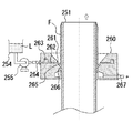
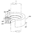
表面層形成用塗布液は、円形スライドホッパー塗布装置を用いて塗布することが好ましい。
以下、円形スライドホッパー塗布装置を用いて表面層形成用塗布液を塗布する方法について具体的に説明する。
The coating solution for forming the surface layer is preferably applied using a circular slide hopper coating device.
Hereinafter, a method for applying the surface layer forming coating solution using the circular slide hopper coating apparatus will be described in detail.
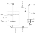
図2および図3に示すように、円形スライドホッパー塗布装置は、円筒状の基材251と、その周囲を取り囲むように設けられた環状の塗布ヘッド260と、塗布液Lを貯留する貯留タンク254とから構成される。
As shown in FIGS. 2 and 3, the circular slide hopper coating apparatus includes a
ここでいう基材251は、表面層形成用塗布液が塗布されるべき基材であり、例えば導電性支持体上に中間層および感光層が形成された状態のもの(表面層が形成されていないもの)である。
The
塗布ヘッド260には、基材251側に開口する塗布液流出口261を有する幅狭の塗布液分配スリット262が基材251の長手方向に垂直な方向に沿って環状の塗布ヘッド260の全周にわたって形成されている。この塗布液分配スリット262は、環状の塗布液分配室263に連通し、この塗布液分配室263は、貯留タンク254内の塗布液Lが圧送ポンプ255により供給管264を介して供給されるよう形成されている。
塗布液分配スリット262の塗布液流出口261の下側には、連続して下方に傾斜し基材251の外寸よりやや大なる寸法で終端をなすように形成されたスライド面265が形成されており、さらに、このスライド面265終端より下方に延びる唇状部(ビード;液溜まり部)266が形成されている。
The
On the lower side of the coating
このような円形スライドホッパー塗布装置においては、基材251を矢印方向に移動させる過程で、塗布液Lを塗布液分配スリット262から押し出し、スライド面265に沿って流下させると、スライド面265終端に至った塗布液Lは、そのスライド面265終端と、基材251の外周面との間にビードを形成した後、基材251表面に塗布されて塗膜Fが形成され、過剰な塗布液Lは排出口267から排出される。
In such a circular slide hopper coating apparatus, when the coating liquid L is pushed out from the coating liquid distribution slit 262 and allowed to flow down along the
このような円形スライドホッパー塗布装置を用いる塗布方法では、スライド面終端と基材は、ある間隙(約2μm〜2mm)を持って配置されているため基材を傷つけることなく、また性質の異なる層を多層形成させる場合においても、既に塗布された層を損傷することなく塗布できる。さらに性質が異なり同一溶媒に溶解する層を多層形成させる際にも、浸漬コーティング方法と比べて溶媒中に存在する時間がはるかに短いので、下層成分が上層側へ殆ど溶出せず、塗布槽にも溶出することなく塗布できるので、例えば無機微粒子や有機樹脂微粒子の分散性を劣化させずに塗布することができる。 In such a coating method using a circular slide hopper coating apparatus, the slide surface end and the base material are arranged with a certain gap (about 2 μm to 2 mm), so that the base material is not damaged and the layers have different properties. Even in the case of forming a multilayer, it can be applied without damaging the already applied layer. Furthermore, when multiple layers with different properties and dissolved in the same solvent are formed, the time in the solvent is much shorter compared to the dip coating method, so that the lower layer component hardly elutes to the upper layer side, so Can also be applied without degrading the dispersibility of inorganic fine particles or organic resin fine particles, for example.
塗膜は、乾燥しないで硬化処理を行ってもよいが、自然乾燥または熱乾燥を行った後、硬化処理を行うことが好ましい。 The coating film may be cured without being dried, but it is preferable to perform the curing treatment after natural drying or heat drying.
乾燥の条件は、溶媒の種類、膜厚などによって適宜選択できる。乾燥温度は、好ましくは室温〜180℃であり、特に好ましくは80〜140℃である。乾燥時間は、好ましくは1分間〜200分間であり、特に好ましくは5分間〜100分間である。 Drying conditions can be appropriately selected depending on the type of solvent, film thickness, and the like. The drying temperature is preferably room temperature to 180 ° C, particularly preferably 80 to 140 ° C. The drying time is preferably 1 minute to 200 minutes, and particularly preferably 5 minutes to 100 minutes.
ラジカル重合性化合物を重合反応させる方法としては、電子線開裂で反応する方法、ラジカル重合開始剤を添加して、光、熱で反応する方法などが挙げられる。ラジカル重合開始剤は光重合開始剤、熱重合開始剤のいずれも使用することができる。また、光重合開始剤および熱重合開始剤を併用することもできる。 Examples of the method of polymerizing the radical polymerizable compound include a method of reacting by electron beam cleavage, a method of adding a radical polymerization initiator and reacting with light and heat. As the radical polymerization initiator, either a photopolymerization initiator or a thermal polymerization initiator can be used. A photopolymerization initiator and a thermal polymerization initiator can also be used in combination.
ラジカル重合開始剤としては、光重合開始剤が好ましく、中でも、アルキルフェノン系化合物、またはフォスフィンオキサイド系化合物が好ましい。特に、α−ヒドロキシアセトフェノン構造、または、アシルフォスフィンオキサイド構造を有する化合物が好ましい。 As the radical polymerization initiator, a photopolymerization initiator is preferable, and among them, an alkylphenone compound or a phosphine oxide compound is preferable. In particular, a compound having an α-hydroxyacetophenone structure or an acylphosphine oxide structure is preferable.
以下、光重合開始剤としてアシルフォスフィンオキサイド系化合物の具体例を示す。 Hereinafter, specific examples of acylphosphine oxide compounds as photopolymerization initiators are shown.
重合開始剤は1種単独でまたは2種以上を混合して用いてもよい。 The polymerization initiators may be used alone or in combination of two or more.
重合開始剤の添加割合は、ラジカル重合性化合物100質量部に対して0.1〜20質量部であることが好ましく、より好ましくは0.5〜10質量部である。 It is preferable that the addition ratio of a polymerization initiator is 0.1-20 mass parts with respect to 100 mass parts of radically polymerizable compounds, More preferably, it is 0.5-10 mass parts.
硬化処理として塗膜に活性線を照射し、ラジカルを発生させて重合し、かつ分子間および分子内で架橋反応による架橋結合を形成して硬化することにより、硬化樹脂が生成される。活性線としては紫外線や電子線がより好ましく、紫外線が使用しやすく特に好ましい。 As the curing treatment, the coating film is irradiated with actinic radiation, polymerized by generating radicals, and cured by forming a cross-linking bond by a cross-linking reaction between molecules and within the molecule, thereby producing a cured resin. The actinic rays are more preferably ultraviolet rays or electron beams, and ultraviolet rays are particularly preferred because they are easy to use.
紫外線光源としては、紫外線を発生する光源であれば制限なく使用できる。例えば、低圧水銀灯、中圧水銀灯、高圧水銀灯、超高圧水銀灯、カーボンアーク灯、メタルハライドランプ、キセノンランプ、フラッシュ(パルス)キセノンなどを用いることができる。
照射条件はそれぞれのランプによって異なるが、活性線の照射量は、通常5〜500mJ/cm2 、好ましくは5〜100mJ/cm2 である。
ランプの電力は、好ましくは0.1kW〜5kWであり、特に好ましくは、0.5kW〜3kWである。
As the ultraviolet light source, any light source that generates ultraviolet light can be used without limitation. For example, a low pressure mercury lamp, a medium pressure mercury lamp, a high pressure mercury lamp, an ultrahigh pressure mercury lamp, a carbon arc lamp, a metal halide lamp, a xenon lamp, a flash (pulse) xenon, or the like can be used.
Irradiation conditions vary depending on each lamp, but the irradiation amount of active rays is usually 5 to 500 mJ / cm 2 , preferably 5 to 100 mJ / cm 2 .
The power of the lamp is preferably 0.1 kW to 5 kW, particularly preferably 0.5 kW to 3 kW.
電子線源としては、電子線照射装置に格別の制限はなく、一般にはこのような電子線照射用の電子線加速機として、比較的安価で大出力が得られるカーテンビーム方式のものが有効に用いられる。電子線照射の際の加速電圧は、100〜300kVであることが好ましい。吸収線量は、0.5〜10Mradであることが好ましい。 As an electron beam source, there is no particular limitation on the electron beam irradiation apparatus, and generally, an electron beam accelerator for electron beam irradiation is a curtain beam type that is relatively inexpensive and can provide a large output. Used. The acceleration voltage during electron beam irradiation is preferably 100 to 300 kV. The absorbed dose is preferably 0.5 to 10 Mrad.
必要な活性線の照射量を得るための照射時間としては、0.1秒間〜10分間が好ましく、作業効率の観点から0.1秒間〜5分間がより好ましい。 The irradiation time for obtaining the necessary amount of active ray irradiation is preferably 0.1 second to 10 minutes, and more preferably 0.1 second to 5 minutes from the viewpoint of work efficiency.
表面層の形成の工程においては、活性線を照射する前後、および活性線を照射中に乾燥を行うことができ、乾燥を行うタイミングはこれらを組み合わせて適宜選択できる。 In the step of forming the surface layer, drying can be performed before and after irradiation with active rays and during irradiation with active rays, and the timing of drying can be appropriately selected by combining these.
〔画像形成装置〕
本発明の画像形成装置は、感光体と、感光体の表面を帯電させる帯電手段と、当該感光体の表面に静電潜像を形成する露光手段と、静電潜像をトナーにより現像してトナー像を形成する現像手段と、トナー像を転写材に転写する転写手段と、転写材に転写されたトナー像を定着させる定着手段と、感光体上の残留トナーを除去する、ブレードよりなるクリーニング手段とを備え、感光体として本発明の感光体が備えられているものである。
[Image forming apparatus]
The image forming apparatus of the present invention includes a photosensitive member, a charging unit for charging the surface of the photosensitive member, an exposure unit for forming an electrostatic latent image on the surface of the photosensitive member, and developing the electrostatic latent image with toner. Developing means for forming a toner image, transfer means for transferring the toner image to a transfer material, fixing means for fixing the toner image transferred to the transfer material, and cleaning comprising a blade for removing residual toner on the photoreceptor. And a photoconductor of the present invention as a photoconductor.
図4は、本発明の画像形成装置の一例における構成を示す説明用断面図である。
この画像形成装置は、タンデム型カラー画像形成装置と称せられるもので、4組の画像形成部(画像形成ユニット)10Y、10M、10C、10Bkと、無端ベルト状中間転写体ユニット7と、給紙手段21および定着手段24とから成る。画像形成装置の本体Aの上部には、原稿画像読み取り装置SCが配置されている。
FIG. 4 is a cross-sectional view illustrating the configuration of an example of the image forming apparatus of the present invention.
This image forming apparatus is called a tandem color image forming apparatus, and includes four sets of image forming units (image forming units) 10Y, 10M, 10C, and 10Bk, an endless belt-shaped intermediate
イエロー色の画像を形成する画像形成部10Yは、ドラム状の感光体1Yの周囲に配置された帯電手段2Y、露光手段3Y、現像手段4Y、一次転写手段としての一次転写ローラ5Y、クリーニング手段6Yを有する。マゼンタ色の画像を形成する画像形成部10Mは、ドラム状の感光体1M、帯電手段2M、露光手段3M、現像手段4M、一次転写手段としての一次転写ローラ5M、クリーニング手段6Mを有する。シアン色の画像を形成する画像形成部10Cは、ドラム状の感光体1C、帯電手段2C、露光手段3C、現像手段4C、一次転写手段としての一次転写ローラ5C、クリーニング手段6Cを有する。黒色画像を形成する画像形成部10Bkは、ドラム状の感光体1Bk、帯電手段2Bk、露光手段3Bk、現像手段4Bk、一次転写手段としての一次転写ローラ5Bk、クリーニング手段6Bkを有する。本発明の画像形成装置は、感光体1Y、1M、1C、1Bkとして、上記の本発明の感光体を用いる。
The
前記4組の画像形成ユニット10Y、10M、10C、10Bkは、感光体1Y、1M、1C、1Bkを中心に、帯電手段2Y、2M、2C、2Bkと、露光手段3Y、3M、3C、3Bkと、回転する現像手段4Y、4M、4C、4Bk、および、感光体1Y、1M、1C、1Bkをクリーニングするクリーニング手段6Y、6M、6C、6Bkより構成されている。
The four sets of
前記画像形成ユニット10Y、10M、10C、10Bkは、感光体1Y、1M、1C、1Bkにそれぞれ形成するトナー画像の色が異なるだけで、同じ構成であり、画像形成ユニット10Yを例にして詳細に説明する。
The
画像形成ユニット10Yは、像形成体である感光体1Yの周囲に、帯電手段2Y、露光手段3Y、現像手段4Y、クリーニング手段6Yを配置し、感光体1Y上にイエロー(Y)のトナー画像を形成するものである。また、本実施の形態においては、この画像形成ユニット10Yのうち、少なくとも感光体1Y、帯電手段2Y、現像手段4Y、クリーニング手段6Yを一体化するように設けている。
In the
帯電手段2Yは、感光体1Yに対して一様な電位を与える手段である。本発明においては、帯電手段としては、接触または非接触のローラ帯電方式のものなどが挙げられる。
The charging unit 2Y is a unit that applies a uniform potential to the
露光手段3Yは、帯電手段2Yによって一様な電位を与えられた感光体1Y上に、画像信号(イエロー)に基づいて露光を行い、イエローの画像に対応する静電潜像を形成する手段であって、この露光手段3Yとしては、感光体1Yの軸方向にアレイ状に発光素子を配列したLEDと結像素子とから構成されるもの、あるいは、レーザー光学系などが用いられる。
The
現像手段4Yは、例えばマグネットを内蔵し現像剤を保持して回転する現像スリーブおよび感光体とこの現像スリーブとの間に直流および/または交流バイアス電圧を印加する電圧印加装置よりなるものである。 The developing means 4Y includes, for example, a developing sleeve that contains a magnet and rotates while holding the developer, and a voltage applying device that applies a DC and / or AC bias voltage between the photosensitive member and the developing sleeve.
定着手段24は、例えば、内部に加熱源を備えた加熱ローラと、この加熱ローラに定着ニップ部が形成されるよう圧接された状態で設けられた加圧ローラとにより構成されてなる熱ローラ定着方式のものが挙げられる。
The fixing
クリーニング手段6Yは、クリーニングブレードと、このクリーニングブレードより上流側に設けられたブラシローラーとにより構成される。
The
具体的には、図5に示すように、クリーニング手段6は、先端が感光体1表面に当接するよう設けられたクリーニングブレード66Aと、このクリーニングブレード66Aより上流側に設けられた、感光体1表面に接触するブラシローラー66Cとにより構成される。
Specifically, as shown in FIG. 5, the cleaning means 6 includes a
クリーニングブレード66Aは、感光体1に付着した残留トナーを除去する機能と共に、感光体1表面を擦過する機能を有する。
The
クリーニングブレード66Aは、支持部材66Bによって支持されている。クリーニングブレード66Aの材質としては、ゴム弾性体が用いられ、その材料としてはウレタンゴム、シリコンゴム、フッ素ゴム、クロロピレンゴム、ブタジエンゴムなどが知られているが、これらのうち、ウレタンゴムは他のゴムに比して摩耗特性が優れている点で特に好ましい。
The
支持部材66Bは、板状の金属部材やプラスチック部材により構成されている。金属部材としては、ステンレス鋼板、アルミ板、制震鋼板などが挙げられる。
The
本発明において、感光体1表面に当接するクリーニングブレード66Aの先端部は、感光体1の回転方向と反対方向(カウンター方向)に向けて負荷をかけた状態で当接することが好ましい。図5に示すように、クリーニングブレード66Aの先端部は感光体1と当接するときに、当接面を形成することが好ましい。
In the present invention, it is preferable that the tip of the
クリーニングブレード66Aの感光体1への当接荷重P、当接角θの好ましい値としては、P=5〜40N/m、θ=5〜35°である。
Preferable values of the contact load P and contact angle θ of the
当接荷重Pはクリーニングブレード66Aをドラム状の感光体1に当接させたときの当接力P′の法線方向ベクトル値である。
また、当接角θは感光体1の当接点Aにおける接線Xと変形前のブレードとのなす角を表す。
The contact load P is a normal vector value of the contact force P ′ when the
Further, the contact angle θ represents an angle formed between the tangent line X at the contact point A of the
66Eは支持部材66Bを回転可能にする回転軸であり、66Gは荷重バネである。
66E is a rotation shaft that enables the
自由長Lは、6〜15mmであることが好ましい。
クリーニングブレード66Aの自由長Lとは、図5に示すように、支持部材66Bの端部Bの位置から変形前のクリーニングブレード66Aの先端点の長さをいう。
The free length L is preferably 6 to 15 mm.
As shown in FIG. 5, the free length L of the
クリーニングブレード66Aの厚さtは、0.5〜10mmであることが好ましい。
ここで、クリーニングブレード66Aの厚さtとは、図5に示すように、支持部材66Bの接着面に対して垂直な方向の長さをいう。
The thickness t of the
Here, the thickness t of the
ブラシローラー66Cは、感光体1に付着した残留トナーの除去、クリーニングブレード66Aで除去された残留トナーの回収機能と共に、感光体1表面を擦過する機能を有する。すなわち、ブラシローラー66Cは、感光体1表面と接触し、その接触部においては、感光体1と進行方向が同方向に回転し、感光体1上の残留トナーや紙粉を除去すると共に、クリーニングブレード66Aで除去された残留トナーを搬送し、搬送スクリュー66Jに回収する。そして、感光体1表面を削り取り、リフレッシュさせる。
The
ブラシローラー66Cに除去手段としてのフリッカ66Iを当接させることにより、感光体1からブラシローラー66Cに転移した残留トナーなどの除去物を除去することが好ましい。更にこのフリッカ66Iに付着したトナーをスクレーパ66Dで除去し、トナーを搬送スクリュー66Jに回収する。回収されたトナーは廃棄物として外部に取り出されるか、またはトナーリサイクル用のリサイクルパイプ(図示せず)を経由して現像器に搬送され再利用される。
It is preferable to remove a removed matter such as residual toner transferred from the
フリッカ66Iは、ステンレス、アルミニウムなどの金属管が好ましく用いられる。
スクレーパ66Dは、リン青銅板、ポリエチレンテレフタレート板、ポリカーボネート板などの弾性板が用いられ、先端がフリッカ66Iの回転方向に対し鋭角を形成するカウンター方式で当接させることが好ましい。
As the flicker 66I, a metal tube such as stainless steel or aluminum is preferably used.
The
このクリーニング手段6においては、感光体1の表面に潤滑剤を塗布する潤滑剤塗布機構が備えられている。
具体的には、荷重バネ66Sによってブラシローラー66Cに押圧された、潤滑剤の固形材料66Kが設けられており、ブラシローラー66Cが回転することにより、固形材料66Kが擦過されて、感光体1表面に潤滑剤が塗布される。
潤滑剤としては、例えばステアリン酸亜鉛などを用いることができる。
The
Specifically, a lubricant
As the lubricant, for example, zinc stearate can be used.
ブラシローラー66Cとしては、導電性または半導電性のブラシローラーが用いられる。ブラシローラー66Cのブラシ構成素材は、任意のものを用いることができるが、疎水性で、かつ誘電率が高い繊維形成性高分子重合体を用いることが好ましい。このような高分子重合体としては、例えば、レーヨン、ナイロン、ポリカーボネート、ポリエステル、メタクリル酸樹脂、アクリル樹脂、ポリ塩化ビニル、ポリ塩化ビニリデン、ポリプロピレン、ポリスチレン、ポリビニルアセテート、スチレン−ブタジエン共重合体、塩化ビニリデン−アクリロニトリル共重合体、塩化ビニル−酢酸ビニル共重合体、塩化ビニル−酢酸ビニル−無水マレイン酸共重合体、シリコーン樹脂、シリコーン−アルキッド樹脂、フェノールホルムアルデヒド樹脂、スチレン−アルキッド樹脂、ポリビニルアセタール(例えばポリビニルブチラール)などが挙げられる。これらの樹脂は単独であるいは2種以上の混合物として用いることができる。特に、好ましくはレーヨン、ナイロン、ポリエステル、アクリル樹脂、ポリプロピレンである。
As the
ブラシローラー66Cは、導電性または半導電性のものを用いることもでき、構成素材にカーボンなどの低抵抗物質を含有させ、任意の比抵抗に調整したものを使用することができる。
As the
ブラシローラー66Cに用いるブラシ毛1本の太さは、5〜20デニールが好ましい。ブラシ毛の太さが5〜20デニールであることにより、感光体1表面より付着物を確実に除去する十分な擦過力を付与するとともに、感光体1表面への傷発生や摩耗を進行させるおそれがないので好ましい。
「デニール」とは、ブラシローラー66Cを構成するブラシ毛(繊維)の長さ9000mの質量をg(グラム)単位で測定した数値である。
The thickness of one bristle used for the
“Denier” is a numerical value obtained by measuring a mass of 9000 m of the bristle (fiber) constituting the
ブラシローラー66Cのブラシ毛密度は、4.5×10² /cm2 〜2.0×10⁴ /cm2 (1平方センチあたりのブラシ毛数)である。
ブラシ毛密度が4.5×10² /cm2 未満であると、剛直度が低く擦過力が弱い上に、擦過にムラができ、付着物を均一に除去することができない。2.0×10⁴ /cm2 より大きいと、剛直になって擦過力が強くなるために感光体1を過度に摩耗させ、感度低下によるカブリや傷による黒スジなどの不良画像が発生する。
The brush hair density of the
When the brush bristle density is less than 4.5 × 10 2 / cm 2 , the rigidity is low and the rubbing force is weak, and the rubbing is uneven and the deposits cannot be removed uniformly. If it is larger than 2.0 × 10 4 / cm 2 , it becomes rigid and the rubbing force becomes strong, so that the
ブラシローラー66Cの感光体1に対する食い込み量は0.4〜1.5mmに設定されることが好ましい。
この食い込み量は、感光体1ドラムとブラシローラー66Cの相対運動によって発生するブラシローラー66Cにかかる負荷を意味する。この負荷は、感光体1ドラムから見れば、ブラシローラー66Cから受ける擦過力に相当し、その範囲を規定することは、感光体1が適度な力で擦過されることが必要であることを意味する。
また、食い込み量とは、ブラシローラー66Cを感光体1に当接させたとき、ブラシ毛が感光体1表面で曲がらずに、直線的に内部に進入したと仮定した時の内部への食い込み長さをいう。
The biting amount of the
This amount of biting means the load on the
Further, the amount of biting in is the length of biting into the interior when it is assumed that the brush bristles enter the interior linearly without bending on the surface of the
ブラシローラー66Cに用いられるローラー部の芯材としては、主としてステンレス、アルミニウムなどの金属、紙、プラスチックなどが用いられるが、これらにより限定されるものではない。
As the core material of the roller portion used for the
ブラシローラー66Cは、その当接部分が感光体1の表面と同方向に移動するように回転するのが好ましい。当接部分が逆方向に移動すると、感光体1の表面に過剰なトナーが存在した場合に、ブラシローラー66Cにより除去されたトナーがこぼれて記録紙や装置を汚す場合がある。
感光体1とブラシローラー66Cとが、同方向に移動する場合に、両者の表面速度比は1対1.1〜1対2の範囲内の値であることが好ましい。
The
When the
本発明の画像形成装置としては、上述の感光体と、現像手段、クリーニング手段などの構成要素をプロセスカートリッジ(画像形成ユニット)として一体に結合して構成し、この画像形成ユニットを装置本体に対して着脱自在に構成しても良い。また、帯電手段、露光手段、現像手段、転写手段、およびクリーニング手段の少なくとも1つを感光体とともに一体に支持してプロセスカートリッジ(画像形成ユニット)を形成し、装置本体に着脱自在の単一画像形成ユニットとし、装置本体のレールなどの案内手段を用いて着脱自在の構成としても良い。 The image forming apparatus of the present invention is configured by integrally combining the above-described photosensitive member, developing unit, cleaning unit and the like as a process cartridge (image forming unit), and this image forming unit is connected to the apparatus main body. It may be configured to be detachable. In addition, a process cartridge (image forming unit) is formed by integrally supporting at least one of a charging unit, an exposure unit, a developing unit, a transfer unit, and a cleaning unit together with a photosensitive member, and is detachably attached to the apparatus main body. It is good also as a formation unit and a structure which can be attached or detached using guide means, such as a rail of an apparatus main body.
無端ベルト状中間転写体ユニット7は、複数のローラにより巻回され、回動可能に支持された半導電性エンドレスベルト状の第2の像担持体としての無端ベルト状中間転写体70を有する。
The endless belt-like intermediate
画像形成ユニット10Y、10M、10C、10Bkより形成された各色の画像は、一次転写手段としての一次転写ローラ5Y、5M、5C、5Bkにより、回動する無端ベルト状中間転写体70上に逐次転写されて、合成されたカラー画像が形成される。給紙カセット20内に収容された転写材(定着された最終画像を担持する画像支持体:例えば普通紙、透明シートなど)Pは、給紙手段21により給紙され、複数の中間ローラ22A、22B、22C、22D、レジストローラ23を経て、二次転写手段としての二次転写ローラ5bに搬送され、転写材P上に二次転写してカラー画像が一括転写される。カラー画像が転写された転写材Pは、定着手段24により定着処理され、排紙ローラ25に挟持されて機外の排紙トレイ26上に載置される。ここで、中間転写体や転写材などの感光体上に形成されたトナー画像の転写支持体を総称して転写媒体と云う。
Each color image formed by the
一方、二次転写手段としての二次転写ローラ5bにより転写材Pにカラー画像を転写した後、転写材Pを曲率分離した無端ベルト状中間転写体70は、クリーニング手段6bにより残留トナーが除去される。
On the other hand, after the color image is transferred to the transfer material P by the
画像形成処理中、一次転写ローラ5Bkは常時、感光体1Bkに当接している。他の一次転写ローラ5Y、5M、5Cはカラー画像形成時にのみ、それぞれ対応する感光体1Y、1M、1Cに当接する。
During the image forming process, the primary transfer roller 5Bk is always in contact with the photoreceptor 1Bk. The other
二次転写ローラ5bは、ここを転写材Pが通過して二次転写が行われる時にのみ、無端ベルト状中間転写体70に当接する。
The
また、装置本体Aから筐体8を支持レール82L、82Rを介して引き出し可能にしてある。
Further, the
筐体8は、画像形成部10Y、10M、10C、10Bkと、無端ベルト状中間転写体ユニット7とから成る。
The
画像形成部10Y、10M、10C、10Bkは、垂直方向に縦列配置されている。感光体1Y、1M、1C、1Bkの図示左側方には無端ベルト状中間転写体ユニット7が配置されている。無端ベルト状中間転写体ユニット7は、ローラ71、72、73、74を巻回して回動可能な無端ベルト状中間転写体70、一次転写ローラ5Y、5M、5C、5Bk、およびクリーニング手段6bとから成る。
The
なお、図4に示す画像形成装置では、カラーのレーザプリンタを示したが、モノクローのレーザプリンタやコピーにも同様に適用可能である。また、露光光源もレーザー以外の光源、例えばLED光源を用いてもよい。 In the image forming apparatus shown in FIG. 4, a color laser printer is shown, but the present invention can be similarly applied to a monochrome laser printer and a copy. The exposure light source may also be a light source other than a laser, such as an LED light source.
本発明の画像形成装置において使用されるトナーとしては、特に限定されないが、真球を100とする形状係数SFが140未満のトナーが好ましい。この形状係数SFが140未満であれば、良好な転写性等が得られ、得られる画像の画質が向上する。トナーを構成するトナー粒子は、高画質化を企図する観点からすれば、その体積平均粒径が2〜8μmであることが好ましい。 The toner used in the image forming apparatus of the present invention is not particularly limited, but a toner having a true sphere of 100 and a shape factor SF of less than 140 is preferable. If the shape factor SF is less than 140, good transferability and the like are obtained, and the image quality of the obtained image is improved. The toner particles constituting the toner preferably have a volume average particle diameter of 2 to 8 μm from the viewpoint of achieving high image quality.
トナー粒子は、通常、結着樹脂および着色剤が含有され、所望により離型剤が含有される。この結着樹脂、着色剤および離型剤はいずれも、従来トナーに用いられている材料を用いることができ、特に制限されない。 The toner particles usually contain a binder resin and a colorant, and optionally contain a release agent. Any of the binder resin, the colorant, and the release agent may be any material that has been used in conventional toners, and is not particularly limited.
上記のトナー粒子を製造する方法としては、特に制約されないが、例えば、通常の粉砕法や、分散媒中で作成する湿式溶融球形化法や、懸濁重合、分散重合、乳化重合凝集法等の既知の重合法などが挙げられる。 The method for producing the toner particles is not particularly limited, and examples thereof include a normal pulverization method, a wet melt spheronization method prepared in a dispersion medium, suspension polymerization, dispersion polymerization, and emulsion polymerization aggregation method. Examples include known polymerization methods.
また、上記トナー粒子に、外添剤として、平均粒径10〜300nm程度のシリカおよびチタニア等の無機微粒子、0.2〜3μm程度の研磨剤を適宜量外添することができる。また、上記トナー粒子と、平均粒径25〜45μmのフェライトビーズ等からなるキャリアを混合して二成分現像剤として用いることができる。 Further, as the external additive, inorganic fine particles such as silica and titania having an average particle diameter of about 10 to 300 nm and an abrasive of about 0.2 to 3 μm can be externally added to the toner particles as appropriate. Further, the toner particles and a carrier composed of ferrite beads having an average particle diameter of 25 to 45 μm can be mixed and used as a two-component developer.
以下、実施例を挙げて本発明を詳細に説明するが、本発明は以下の実施例のみに限定されるものではない。なお、下記中「部」とは「質量部」を示す。 EXAMPLES Hereinafter, although an Example is given and this invention is demonstrated in detail, this invention is not limited only to a following example. In the following, “part” means “part by mass”.
〔感光体の作製例1〕
直径60mmのアルミニウム製の円筒体の表面を切削加工し、表面を細かく粗面にした導電性支持体〔1〕を用意した。
[Photosensitive body preparation example 1]
The surface of an aluminum cylinder having a diameter of 60 mm was cut to prepare a conductive support [1] having a fine and rough surface.
(中間層の形成)
下記組成の分散液を下記溶媒と同じ溶媒にて二倍に希釈し、一夜静置後に濾過(フィルター;日本ポール社製リジメッシュ5μmフィルター使用)し、中間層形成用塗布液〔1〕を調製した。
バインダー樹脂:ポリアミド樹脂「CM8000」(東レ社製) 1部
金属酸化物粒子:酸化チタン「SMT500SAS」(テイカ社製) 3部
溶媒:メタノール 10部
分散機としてサンドミルを用いて、バッチ式で10時間の分散を行った。
中間層形成用塗布液〔1〕を用いて導電性支持体〔1〕上に、浸漬コーティング法で塗布し、乾燥膜厚2μmの中間層〔1〕を形成した。
(Formation of intermediate layer)
A dispersion having the following composition was diluted twice with the same solvent as described below, and allowed to stand overnight, followed by filtration (filter; using a lymesh 5 μm filter manufactured by Nihon Pall Co., Ltd.) to prepare an intermediate layer forming coating solution [1]. .
Binder resin: Polyamide resin “CM8000” (manufactured by Toray Industries, Inc.) 1 part Metal oxide particles: Titanium oxide “SMT500SAS” (manufactured by Teica) 3 parts Solvent: Methanol 10 parts Batch using a sand mill as a disperser for 10 hours Was distributed.
An intermediate layer [1] having a dry film thickness of 2 μm was formed on the conductive support [1] using the intermediate layer forming coating solution [1] by dip coating.
(電荷発生層の形成)
電荷発生物質:下記顔料(CG−1)20部、バインダー樹脂:ポリビニルブチラール樹脂「#6000−C」(電気化学工業社製)10部、溶媒:酢酸t−ブチル700部、溶媒:4−メトキシ−4−メチル−2−ペンタノン300部を混合し、サンドミルを用いて10時間分散し、電荷発生層形成用塗布液〔1〕を調製した。この電荷発生層形成塗布液〔1〕を中間層〔1〕上に浸漬コーティング法で塗布し、乾燥膜厚0.3μmの電荷発生層〔1〕を形成した。
(Formation of charge generation layer)
Charge generation material: 20 parts of the following pigment (CG-1), binder resin: 10 parts of polyvinyl butyral resin “# 6000-C” (manufactured by Denki Kagaku Kogyo), solvent: 700 parts of t-butyl acetate, solvent: 4-methoxy 300 parts of -4-methyl-2-pentanone was mixed and dispersed for 10 hours using a sand mill to prepare a coating solution [1] for forming a charge generation layer. This charge generation layer forming coating solution [1] was applied onto the intermediate layer [1] by a dip coating method to form a charge generation layer [1] having a dry film thickness of 0.3 μm.
<顔料(CG−1)の合成>
(1)無定形チタニルフタロシアニンの合成
1,3−ジイミノイソインドリン;29.2部をo−ジクロロベンゼン200部に分散し、チタニウムテトラ−n−ブトキシド;20.4部を加えて窒素雰囲気下に150〜160℃で5時間加熱した。放冷後、析出した結晶を濾過し、クロロホルムで洗浄、2%塩酸水溶液で洗浄、水洗メタノール洗浄して、乾燥後、26.2部(収率91%)の粗チタニルフタロシアニンを得た。
次いで、粗チタニルフタロシアニンを5℃以下において濃硫酸250部中で1時間攪拌して溶解し、これを20℃の水5000部に注いだ。析出した結晶をろ過し、充分に水洗してウエットペースト品225部を得た。
このウエットペースト品を冷凍庫にて凍結し、再度解凍した後、ろ過、乾燥して無定形チタニルフタロシアニン24.8部(収率86%)を得た。
<Synthesis of Pigment (CG-1)>
(1) Synthesis of
Next, the crude titanyl phthalocyanine was dissolved by stirring for 1 hour in 250 parts of concentrated sulfuric acid at 5 ° C. or less, and this was poured into 5000 parts of water at 20 ° C. The precipitated crystals were filtered and sufficiently washed with water to obtain 225 parts of a wet paste product.
This wet paste product was frozen in a freezer, thawed again, filtered and dried to obtain 24.8 parts of amorphous titanyl phthalocyanine (yield 86%).
(2)(2R,3R)−2,3−ブタンジオール付加体チタニルフタロシアニン(CG−1)の合成
上記無定形チタニルフタロシアニン10.0部と(2R,3R)−2,3−ブタンジオール0.94部(0.6当量比)(当量比はチタニルフタロシアニンに対する当量比、以後同じ)をオルトクロロベンゼン(ODB)200部中に混合し60〜70℃で6.0時間加熱撹拌した。一夜放置後、該反応液にメタノールを加えて生じた結晶を濾過し、濾過後の結晶をメタノールで洗って((2R,3R)−2,3−ブタンジオール付加体チタニルフタロシアニンを含有する顔料)CG−1:10.3部を得た。顔料(CG−1)のX線回折スペクトルでは、8.3°、24.7°、25.1°、26.5°に明確なピークがある。マススペクトルにおいて576と648にピークがあり、IRスペクトルでは970cm-1付近のTi=O、630cm-1付近にO−Ti−Oの両吸収が現れる。また熱分析(TG)では390〜410℃に約7%の質量減少があることから、チタニルフタロシアニンと(2R,3R)−2,3−ブタンジオールの1:1付加体と非付加体(付加していない)チタニルフタロシアニンの混合物と推定される。
得られた顔料(CG−1)のBET比表面積を流動式比表面積自動測定装置(マイクロメトリックス・フローソープ型:島津製作所)で測定したところ、31.2m2 /gであった。
(2) Synthesis of (2R, 3R) -2,3-butanediol adduct titanyl phthalocyanine (CG-1) 10.0 parts of the above amorphous titanyl phthalocyanine and (2R, 3R) -2,3-butanediol 94 parts (0.6 equivalent ratio) (equivalent ratio is equivalent ratio to titanyl phthalocyanine, hereinafter the same) was mixed in 200 parts of orthochlorobenzene (ODB) and stirred at 60 to 70 ° C. for 6.0 hours. After standing overnight, methanol was added to the reaction solution, and the resulting crystals were filtered. The crystals after filtration were washed with methanol (a pigment containing (2R, 3R) -2,3-butanediol adduct titanyl phthalocyanine). CG-1: 10.3 parts were obtained. In the X-ray diffraction spectrum of the pigment (CG-1), there are clear peaks at 8.3 °, 24.7 °, 25.1 °, and 26.5 °. There is a peak in the 576 and 648 in the mass spectra, O-Ti-O both absorption appears Ti = O near 970 cm -1, around 630 cm -1 in the IR spectrum. In addition, since thermal analysis (TG) has a mass loss of about 7% at 390 to 410 ° C., a 1: 1 adduct and a non-adduct (addition) of titanyl phthalocyanine and (2R, 3R) -2,3-butanediol (Not) presumed to be a mixture of titanyl phthalocyanine.
It was 31.2 m < 2 > / g when the BET specific surface area of the obtained pigment (CG-1) was measured with the flow type specific surface area automatic measuring apparatus (Micrometrics flow soap type: Shimadzu Corporation).
(電荷輸送層の形成)
電荷輸送物質:下記化合物A225部、バインダー樹脂:ポリカーボネート樹脂「Z300」(三菱ガス化学社製)300部、酸化防止剤:「Irganox1010」(日本チバガイギー社製)6部、溶媒:THF(テトラヒドロフラン)1600部、溶媒:トルエン400部、シリコーンオイル「KF−50」(信越化学社製)1部を混合し、溶解して電荷輸送層形成用塗布液〔1〕を調製した。
この電荷輸送層形成用塗布液〔1〕を電荷発生層〔1〕の上に円形スライドホッパー塗布装置を用いて塗布し、乾燥膜厚20μmの電荷輸送層〔1〕を形成した。
(Formation of charge transport layer)
Charge transport material: 225 parts of the following compound A, binder resin: 300 parts of polycarbonate resin “Z300” (manufactured by Mitsubishi Gas Chemical), antioxidant: 6 parts of “Irganox 1010” (manufactured by Ciba Geigy Japan), solvent: THF (tetrahydrofuran) 1600 Part, solvent: 400 parts of toluene and 1 part of silicone oil “KF-50” (manufactured by Shin-Etsu Chemical Co., Ltd.) were mixed and dissolved to prepare a coating solution [1] for forming a charge transport layer.
The charge transport layer forming coating solution [1] was applied onto the charge generation layer [1] using a circular slide hopper coating apparatus to form a charge transport layer [1] having a dry film thickness of 20 μm.
(表面層の形成)
(1)表面処理を施した有機樹脂微粒子の作製
メタノール20gに水2gを添加し、撹拌した。ここに濃塩酸を加えpHを2〜3に調整した。この溶液にシランカップリング剤として上記例示化合物(C−5)2.5gを添加し、室温にて1時間撹拌した。次いで、メラミン樹脂「エポスターS6」(平均粒径:400nm、日本触媒社製)の濃度が10質量%のメタノール分散液を加え40℃にて2時間撹拌した。加熱撹拌終了後、飽和炭酸水素ナトリウム水溶液に注ぎ中和した。中和後、濾別し120℃にて2時間乾燥させて、表面処理を行った。得られた微粒子を有機樹脂微粒子〔1〕とした。
(Formation of surface layer)
(1) Preparation of surface-treated organic resin fine particles 2 g of water was added to 20 g of methanol and stirred. Concentrated hydrochloric acid was added thereto to adjust the pH to 2-3. To this solution, 2.5 g of the exemplified compound (C-5) was added as a silane coupling agent, and the mixture was stirred at room temperature for 1 hour. Subsequently, a methanol dispersion having a concentration of 10% by mass of melamine resin “Eposter S6” (average particle diameter: 400 nm, manufactured by Nippon Shokubai Co., Ltd.) was added and stirred at 40 ° C. for 2 hours. After completion of heating and stirring, the mixture was neutralized by pouring into a saturated aqueous sodium hydrogen carbonate solution. After neutralization, it was filtered off and dried at 120 ° C. for 2 hours for surface treatment. The obtained fine particles were designated as organic resin fine particles [1].
(2)表面層の形成
無機微粒子〔1〕:酸化スズ(平均粒径:20nm)85部、有機樹脂微粒子〔1〕25部、多官能ラジカル重合性化合物:上記例示化合物(M1)100部、溶媒:2−ブタノール400部、溶媒:THF(テトラヒドロフラン)40部を遮光下で混合し、分散機としてサンドミルを用いて5時間分散した後、重合開始剤:上記例示化合物(P2)10部を加え、遮光下で撹拌して溶解させ、表面層形成用塗布液〔1〕を調製した。この表面層形成用塗布液〔1〕を電荷輸送層〔1〕上に円形スライドホッパー塗布装置を用いて塗布して塗膜を形成し、メタルハライドランプを用いて紫外線を1分間照射して、乾燥膜厚5.0μmの表面層〔1〕を形成し感光体〔1〕を作製した。表面層〔1〕中の無機微粒子の数平均一次粒径は20nm、有機樹脂微粒子の数平均一次粒径は400nmであった。
(2) Formation of surface layer Inorganic fine particles [1]: 85 parts of tin oxide (average particle size: 20 nm), 25 parts of organic resin fine particles [1], polyfunctional radical polymerizable compound: 100 parts of the above exemplified compound (M1), Solvent: 400 parts of 2-butanol, solvent: 40 parts of THF (tetrahydrofuran) were mixed in the dark and dispersed for 5 hours using a sand mill as a disperser. Then, polymerization initiator: 10 parts of the exemplified compound (P2) was added. Then, the mixture was stirred and dissolved under light shielding to prepare a surface layer forming coating solution [1]. The surface layer forming coating solution [1] is applied onto the charge transport layer [1] using a circular slide hopper coating device to form a coating film, and irradiated with ultraviolet rays for 1 minute using a metal halide lamp, followed by drying. A surface layer [1] having a thickness of 5.0 μm was formed to produce a photoreceptor [1]. The number average primary particle size of the inorganic fine particles in the surface layer [1] was 20 nm, and the number average primary particle size of the organic resin fine particles was 400 nm.
〔感光体の作製例2〜8〕
感光体の作製例1における表面層の形成において、用いる無機微粒子および有機樹脂微粒子の種類を表1に従って変更したことの他は同様にして、感光体〔2〕〜〔8〕を作製した。
[Photosensitive member production examples 2 to 8]
Photoreceptors [2] to [8] were produced in the same manner as in the formation of the surface layer in Photoreceptor Production Example 1, except that the types of inorganic fine particles and organic resin fine particles used were changed according to Table 1.
表1において、無機微粒子〔3〕,〔4〕,〔6〕,〔7〕は、コア−シェル構造の複合微粒子であって、下記の作製方法によって得られたものである。
また、表1において、有機樹脂微粒子〔2〕〜〔7〕は、下記の作製方法によって得られたものである。有機樹脂微粒子〔8〕は、表面処理を施さず、メラミン樹脂「エポスターS6」(日本触媒社製)の微粒子をそのまま使用した。
In Table 1, inorganic fine particles [3], [4], [6], [7] are composite fine particles having a core-shell structure, and are obtained by the following production method.
In Table 1, organic resin fine particles [2] to [7] are obtained by the following production method. The organic resin fine particles [8] were not subjected to surface treatment, and the fine particles of the melamine resin “Eposter S6” (manufactured by Nippon Shokubai Co., Ltd.) were used as they were.
<無機微粒子〔3〕の作製>
純水3Lに35%塩酸0.1Lを加えて75℃に加温した。この塩酸酸性液に、平均粒径が200nmであるアルミナ芯材300gを懸濁し、撹拌を行いながら、ここに四塩化チタン水溶液(Ti分として50質量%)を1時間当たり36gの割合で定量添加するとともに、10質量%に溶解した苛性ソーダを1時間当たり360mlの割合で添加した。得られた粒子を含むスラリーを、その導電率が100μS/cm以下となるまでリパルプ洗浄した後、ヌッチェ濾過を行い、ケーキを得、その後150℃で真空乾燥し、アルミナ芯材の表面に酸化チタンが付着されてなる無機微粒子〔3〕を得た。
<Preparation of inorganic fine particles [3]>
To 3 L of pure water, 0.1 L of 35% hydrochloric acid was added and heated to 75 ° C. In this hydrochloric acid acidic solution, 300 g of an alumina core material having an average particle size of 200 nm is suspended, and while stirring, a titanium tetrachloride aqueous solution (50 mass% as Ti content) is added quantitatively at a rate of 36 g per hour. At the same time, caustic soda dissolved in 10% by mass was added at a rate of 360 ml per hour. The slurry containing the obtained particles is repulp washed until the electrical conductivity becomes 100 μS / cm or less, and then subjected to Nutsche filtration to obtain a cake, followed by vacuum drying at 150 ° C., and titanium oxide on the surface of the alumina core material. To obtain inorganic fine particles [3].
<無機微粒子〔4〕の作製>
図6に示す製造装置を用い、硫酸バリウム芯材の表面に酸化スズが付着されてなる無機微粒子〔4〕を作製した。
具体的には、母液槽(11)中に純水3500cm3 を投入し、次に平均粒径が100nmである球状の硫酸バリウム芯材900gを投入して5パス循環させた。母液槽(11)から流出するスラリーの流速は2280cm3 /minであった。また強分散装置(13)の撹拌速度を16000rpmとした。循環完了後のスラリーを純水で全量9000cm3 にメスアップし、そこに1600gの錫酸ナトリウムおよび2.3cm3 の水酸化ナトリウム水溶液(濃度25N)を投入して5パス循環させた。このようにして母液を得た。この母液を、母液槽(11)から流出する流速(S1)が200cm3 となるように循環させながら、強分散装置(13)としてのホモジナイザー「magic LAB」(IKAジャパン株式会社製)に20%硫酸を供給した。供給速度(S3)を9.2cm3 /minとした。ホモジナイザーの容積は20cm3 、撹拌速度は16000rpmであった。循環を15分間行い、その間硫酸を連続的にホモジナイザーに供給した。このようにして、硫酸バリウム芯材の表面に酸化スズの被覆層が形成された粒子を得た。
得られた粒子を含むスラリーを、その導電率が600μS/cm以下となるまでリパルプ洗浄した後、ヌッチェ濾過を行い、ケーキを得た。このケーキを大気中、150℃で10時間乾燥させた。次いで乾燥ケーキを粉砕し、その粉砕粉を1体積%H2 /N2 雰囲気下で450℃、45分間還元焼成した。これによって、硫酸バリウム芯材の表面に酸化スズが付着されてなる無機微粒子〔4〕を得た。
<Preparation of inorganic fine particles [4]>
Using the production apparatus shown in FIG. 6, inorganic fine particles [4] in which tin oxide was adhered to the surface of the barium sulfate core material were produced.
Specifically, 3500 cm 3 of pure water was introduced into the mother liquor tank (11), and then 900 g of a spherical barium sulfate core material having an average particle diameter of 100 nm was introduced and circulated for 5 passes. The flow rate of the slurry flowing out from the mother liquor tank (11) was 2280 cm 3 / min. The stirring speed of the strong dispersion device (13) was 16000 rpm. The slurry after circulation completion females up to a total volume of 9000 cm 3 with pure water and there is 5 the path circulated by introduction of sodium stannate and 2.3 cm 3 of an aqueous sodium hydroxide solution (concentration 25 N) of 1600 g. A mother liquor was thus obtained. While this mother liquor is circulated so that the flow rate (S1) flowing out from the mother liquor tank (11) is 200 cm 3 , it is 20% in a homogenizer “magic LAB” (manufactured by IKA Japan Co., Ltd.) as a strong dispersion device (13). Sulfuric acid was supplied. The supply rate (S3) was set to 9.2 cm 3 / min. The volume of the homogenizer was 20 cm 3 and the stirring speed was 16000 rpm. Circulation was performed for 15 minutes, during which time sulfuric acid was continuously fed to the homogenizer. In this manner, particles having a tin oxide coating layer formed on the surface of the barium sulfate core material were obtained.
The slurry containing the obtained particles was repulp washed until the conductivity became 600 μS / cm or less, and then subjected to Nutsche filtration to obtain a cake. This cake was dried in air at 150 ° C. for 10 hours. Next, the dried cake was pulverized, and the pulverized powder was reduced and fired at 450 ° C. for 45 minutes in a 1% by volume H 2 / N 2 atmosphere. As a result, inorganic fine particles [4] in which tin oxide was adhered to the surface of the barium sulfate core material were obtained.
ここで、図6に示す製造装置において、符号12,14は、母液槽11と強分散装置13との間の循環路を形成する循環配管、符号15,16は、循環配管12,14に設けられたポンプ、符号11aは撹拌翼、符号13aは撹拌部、符号11b,13bはシャフト、符号11c,13cはモーターを示す。
In the manufacturing apparatus shown in FIG. 6,
<無機微粒子〔6〕の作製>
無機微粒子〔3〕の作製において、アルミナ芯材を、平均粒径が250nmであるシリカ芯材に変更したことの他は同様にして、シリカ芯材の表面に酸化チタンが付着されてなる無機微粒子〔6〕を得た。
<Preparation of inorganic fine particles [6]>
In the production of inorganic fine particles [3], inorganic fine particles obtained by attaching titanium oxide to the surface of the silica core material are the same except that the alumina core material is changed to a silica core material having an average particle diameter of 250 nm. [6] was obtained.
<無機微粒子〔7〕の作製>
無機微粒子〔4〕の作製において、硫酸バリウム芯材を、平均粒径が100nmであるアルミナ芯材に変更したことの他は同様にして、アルミナ芯材の表面に酸化スズが付着されてなる無機微粒子〔7〕を得た。
<Preparation of inorganic fine particles [7]>
In the production of the inorganic fine particles [4], the barium sulfate core material was changed to an alumina core material having an average particle diameter of 100 nm. Fine particles [7] were obtained.
<有機樹脂微粒子〔2〕〜〔7〕の作製>
感光体の作製例1における表面処理を施した有機樹脂微粒子の作製において、用いるメラミン樹脂の種類とカップリング剤の種類を表1に従って変更したことの他は同様にして、有機樹脂微粒子〔2〕〜〔7〕を作製した。
<Preparation of organic resin fine particles [2] to [7]>
In the production of the organic resin fine particles subjected to the surface treatment in Preparation Example 1 of the photoreceptor, the organic resin fine particles [2] are the same except that the type of the melamine resin and the type of the coupling agent are changed according to Table 1. To [7] were produced.
得られた有機樹脂微粒子〔1〕〜〔8〕につき、凝集性の評価を行った。
具体的には、酸化スズの濃度が20質量%の2−ブタノール分散液4.8gに有機樹脂微粒子〔1〕〜〔8〕をそれぞれ0.2g添加し、凝集の程度を目視にて観察した。下記評価基準に従って評価した。結果を表2に示す。
−評価基準−
◎:凝集が全く見られない(良好)
○:凝集が軽微に確認される(実用上問題なし)
×:凝集がはっきりと確認される(実用上問題あり)
The obtained organic resin fine particles [1] to [8] were evaluated for aggregability.
Specifically, 0.2 g of organic resin fine particles [1] to [8] were added to 4.8 g of 2-butanol dispersion having a tin oxide concentration of 20% by mass, and the degree of aggregation was visually observed. . Evaluation was performed according to the following evaluation criteria. The results are shown in Table 2.
-Evaluation criteria-
A: No aggregation is observed (good)
○: Slight aggregation is confirmed (no problem in practical use)
X: Aggregation is clearly confirmed (practical problem)
〔実施例1〜7、比較例1〕
基本的に図4に示す画像形成装置の構成と同様の評価機「bizhub PRO C6501」(コニカミノルタ株式会社製)に、感光体〔1〕〜〔8〕をそれぞれ搭載し評価を行った。ここで、感光体〔1〕〜〔7〕を用いて評価を行ったものを実施例1〜7、感光体〔8〕を用いて評価を行ったものを比較例1とした。評価機「bizhub PRO C6501」の露光光源としては、波長780nmの半導体レーザーを用いた。
温度30℃、湿度85%の高温高湿環境下で、画像比率6%の文字画像をA4横送りで各300,000枚両面連続プリントを行う耐久試験を実施し、下記に示す電位安定性、クリーニング性および耐傷性の評価を行った。結果を表2に示す。
[Examples 1 to 7, Comparative Example 1]
Evaluation was performed by mounting the photoreceptors [1] to [8] on an evaluation machine “bizhub PRO C6501” (manufactured by Konica Minolta Co., Ltd.) having the same configuration as that of the image forming apparatus shown in FIG. Here, Examples 1 to 7 were evaluated using the photoreceptors [1] to [7], and Comparative Example 1 was evaluated using the photoreceptor [8]. A semiconductor laser having a wavelength of 780 nm was used as an exposure light source of the evaluation machine “bizhub PRO C6501”.
In a high-temperature and high-humidity environment with a temperature of 30 ° C. and a humidity of 85%, an endurance test was performed in which 300,000 double-sided continuous printing was performed for each character image with an image ratio of 6% by A4 horizontal feed. The cleaning property and scratch resistance were evaluated. The results are shown in Table 2.
(1)電位安定性の評価
耐久試験前後における露光部電位の電位変動の大きさにより評価した。
具体的には、初期の帯電電位を600±50Vに調整し、耐久試験前と300,000枚後の露光部電位の変化量(ΔV)を算出した。下記評価基準に従って評価した。
−評価基準−
◎:ΔVが30V未満(非常に良好)
○:ΔVが30V以上60V未満(良好)
△:ΔVが60V以上100V未満(実用上問題なし)
×:ΔVが100V以上(実用上問題あり)
(1) Evaluation of electric potential stability It evaluated by the magnitude | size of the electric potential fluctuation | variation of the exposure part electric potential before and behind an endurance test.
Specifically, the initial charging potential was adjusted to 600 ± 50 V, and the amount of change (ΔV) in the exposed portion potential before the endurance test and after 300,000 sheets was calculated. Evaluation was performed according to the following evaluation criteria.
-Evaluation criteria-
A: ΔV is less than 30V (very good)
○: ΔV is 30V or more and less than 60V (good)
Δ: ΔV is 60 V or more and less than 100 V (no problem in practical use)
×: ΔV is 100 V or more (there is a problem in practical use)
(2)クリーニング性の評価
耐久試験後におけるクリーニング性を下記評価基準に従って評価した。
判定基準は以下のとおりである。
−評価基準−
◎:トナーすり抜けがなく、ブレード摩耗幅が20μm未満(良好)
○:トナーすり抜けがなく、ブレード摩耗幅が20μm以上(実用上問題なし)
×:トナーすり抜け発生(実用上問題あり)
(2) Evaluation of cleaning property Cleaning property after the durability test was evaluated according to the following evaluation criteria.
The judgment criteria are as follows.
-Evaluation criteria-
A: No toner slipping out, blade wear width less than 20 μm (good)
○: No toner slipping, blade wear width of 20 μm or more (no problem in practical use)
X: Toner slipping out (practical problem)
(3)耐傷性
耐刷試験後において、A3紙全面にハーフトーン画像の画出しを行い、下記評価基準に従って評価した。
−評価基準−
◎:感光体表面に目視でみられる目立った傷の発生はなく、ハーフトーン画像にも感光体傷に対応する画像不良の発生は見あたらない(良好)
○:感光体表面に目視で、軽微な傷の発生があるが、ハーフトーン画像には感光体傷に対応する画像不良の発生は見あたらない(実用上問題なし)
×:感光体表面に目視で、明確に傷の発生があり、ハーフトーン画像にも該傷に対応する画像不良の発生が認められる(実用上問題有り)
(3) Scratch resistance After the printing durability test, a halftone image was drawn on the entire surface of A3 paper and evaluated according to the following evaluation criteria.
-Evaluation criteria-
A: There is no noticeable scratch on the surface of the photoconductor, and no image defect corresponding to the photoconductor is found in the halftone image (good).
○: Minor scratches are visually observed on the surface of the photoconductor, but no image defect corresponding to the photoconductor scratch is found in the halftone image (no problem in practical use).
X: The surface of the photoreceptor is clearly scratched, and the occurrence of image defects corresponding to the scratch is recognized in the halftone image (practically problematic).
表2の結果より、本発明に係る実施例1〜7では、有機樹脂微粒子がカップリング剤によって表面処理が施されたものであることにより、良好な分散性が得られることが確認され、また、電位安定性を確保しながらも良好なクリーニング性を有すると共に、高い耐傷性が得られることが確認された。
比較例1では、有機樹脂微粒子がカップリング剤によって表面処理が施されたものでないため、良好な分散性が得られず、また、クリーニング性および耐傷性が得られないことが確認された。これは、表面層中に、有機樹脂微粒子が凝集体として存在しているためと考えられる。この凝集体は、表面層中にて均一に存在していないため、凝集体が摺擦によって表面層から脱離し易くなり、傷の原因になったと考えられる。また、表面層に傷が入ることによって、表面状態が荒れ、クリーニング性が悪化したと考えられる。
From the results of Table 2, in Examples 1 to 7 according to the present invention, it was confirmed that the organic resin fine particles were surface-treated with a coupling agent, so that good dispersibility was obtained. It was confirmed that while having potential stability, it had good cleaning properties and high scratch resistance.
In Comparative Example 1, since the organic resin fine particles were not subjected to surface treatment with a coupling agent, it was confirmed that good dispersibility could not be obtained, and that cleanability and scratch resistance could not be obtained. This is presumably because the organic resin fine particles are present as aggregates in the surface layer. Since this aggregate does not exist uniformly in the surface layer, it is considered that the aggregate is easily detached from the surface layer by rubbing and causes a scratch. Further, it is considered that the surface condition is roughened and the cleaning property is deteriorated due to the scratch on the surface layer.
1,1Y、1M、1C、1Bk 感光体
2Y、2M、2C、2Bk 帯電手段
3Y、3M、3C、3Bk 露光手段
4Y、4M、4C、4Bk 現像手段
5Y、5M、5C、5Bk 一次転写ローラ
5b 二次転写ローラ
6,6Y、6M、6C、6Bk、6b クリーニング手段
7 中間転写体ユニット
8 筐体
10Y、10M、10C、10Bk 画像形成ユニット
11 母液槽
11a 撹拌翼
11b シャフト
11c モーター
12 循環配管
13 強分散装置
13a 撹拌部
13b シャフト
13c モーター
14 循環配管
15 ポンプ
16 ポンプ
21 給紙手段
20 給紙カセット
22A、22B、22C、22D 中間ローラ
23 レジストローラ
24 定着手段
25 排紙ローラ
26 排紙トレイ
66A クリーニングブレード
66B 支持部材
66C ブラシローラー
66D スクレーパ
66E 回転軸
66G 荷重バネ
66I フリッカ
66J 搬送スクリュー
66S 荷重バネ
66K 固形材料
70 無端ベルト状中間転写体
71、72、73、74 ローラ
82L、82R 支持レール
P 転写材
101 導電性支持体
102 感光層
103 中間層
104 電荷発生層
105 電荷輸送層
106 表面層
107a 有機樹脂微粒子
107b 無機微粒子
251 基材
254 貯留タンク
255 圧送ポンプ
260 塗布ヘッド
261 塗布液流出口
262 塗布液分配スリット
263 塗布液分配室
264 供給管
265 スライド面
266 唇状部
267 排出口
L 塗布液
F 塗膜
1,1Y, 1M, 1C, 1Bk photoconductor 2Y, 2M, 2C, 2Bk charging means 3Y, 3M, 3C, 3Bk exposure means 4Y, 4M, 4C, 4Bk developing means 5Y, 5M, 5C, 5Bk primary transfer roller 5b second Next transfer roller 6, 6Y, 6M, 6C, 6Bk, 6b Cleaning means 7 Intermediate transfer body unit 8 Housing 10Y, 10M, 10C, 10Bk Image forming unit 11 Mother liquid tank 11a Stirring blade 11b Shaft 11c Motor 12 Circulating piping 13 Strong dispersion Device 13a Stirrer 13b Shaft 13c Motor 14 Circulation Piping 15 Pump 16 Pump 21 Paper Feeding Unit 20 Paper Feeding Cassette 22A, 22B, 22C, 22D Intermediate Roller 23 Registration Roller 24 Fixing Unit 25 Paper Discharge Roller 26 Paper Discharge Tray 66A Cleaning Blade 66B Support member 6C Brush roller 66D Scraper 66E Rotating shaft 66G Load spring 66I Flicker 66J Conveying screw 66S Load spring 66K Solid material 70 Endless belt-shaped intermediate transfer member 71, 72, 73, 74 Roller 82L, 82R Support rail P Transfer material 101 Conductive support DESCRIPTION OF SYMBOLS 102 Photosensitive layer 103 Intermediate | middle layer 104 Charge generation layer 105 Charge transport layer 106 Surface layer 107a Organic resin fine particle 107b Inorganic fine particle 251 Base material 254 Storage tank 255 Pressure pump 260 Coating head 261 Coating liquid outlet 262 Coating liquid distribution slit 263 Coating liquid distribution Chamber 264 Supply pipe 265 Slide surface 266 Lip part 267 Discharge port L Coating liquid F Coating film
Claims (11)
前記表面層は、2個以上のラジカル重合性官能基を有する化合物を重合反応することによって得られる硬化樹脂中に、少なくとも表面の一部が金属酸化物によって形成された無機微粒子、および、メラミンおよびベンゾグアナミンのうち少なくとも一種に由来の構成単位を含む樹脂からなる有機樹脂微粒子が含有されてなるものであり、
前記有機樹脂微粒子がカップリング剤によって表面処理が施されたものであることを特徴とする電子写真感光体。 In an electrophotographic photosensitive member in which a photosensitive layer is formed on a conductive support and a surface layer is formed on the photosensitive layer,
The surface layer includes inorganic fine particles in which at least a part of the surface is formed of a metal oxide in a cured resin obtained by polymerizing a compound having two or more radical polymerizable functional groups, and melamine and Organic resin fine particles made of a resin containing a structural unit derived from at least one of benzoguanamine are contained,
An electrophotographic photosensitive member, wherein the organic resin fine particles are surface-treated with a coupling agent.
感光層上に、2個以上のラジカル重合性官能基を有する化合物と、少なくとも表面の一部が金属酸化物によって形成された無機微粒子と、カップリング剤によって表面処理が施された、メラミンおよびベンゾグアナミンのうち少なくとも一種に由来の構成単位を含む樹脂からなる有機樹脂微粒子とを含有する表面層形成用塗布液を塗布して塗布膜を形成し、当該塗布膜を硬化処理する工程を有することを特徴とする電子写真感光体の製造方法。 In the method for producing an electrophotographic photosensitive member in which a photosensitive layer is formed on a conductive support and a surface layer is formed on the photosensitive layer,
Melamine and benzoguanamine, wherein the photosensitive layer has a compound having two or more radically polymerizable functional groups, inorganic fine particles having at least part of the surface formed of a metal oxide, and a surface treatment with a coupling agent. A coating layer is formed by applying a coating solution for forming a surface layer containing organic resin fine particles composed of a resin containing a structural unit derived from at least one of the above, and the coating film is cured. A method for producing an electrophotographic photosensitive member.
前記クリーニング手段がブレードよりなり、
前記電子写真感光体が請求項1〜請求項9のいずれかに記載の電子写真感光体であることを特徴とする画像形成装置。 An electrophotographic photosensitive member; a charging unit that charges the surface of the electrophotographic photosensitive member; an exposing unit that forms an electrostatic latent image on the surface of the electrophotographic photosensitive member; and developing the electrostatic latent image with toner Developing means for forming a toner image by developing with an agent, transfer means for transferring the toner image to a transfer material, fixing means for fixing the toner image transferred to the transfer material, and residual on the electrophotographic photosensitive member Cleaning means for removing toner,
The cleaning means comprises a blade;
An image forming apparatus, wherein the electrophotographic photosensitive member is the electrophotographic photosensitive member according to claim 1.
Priority Applications (3)
| Application Number | Priority Date | Filing Date | Title |
|---|---|---|---|
| JP2013255808A JP5915633B2 (en) | 2013-12-11 | 2013-12-11 | Electrophotographic photosensitive member, method for producing the same, and image forming apparatus |
| CN201410513484.XA CN104516218B (en) | 2013-10-04 | 2014-09-29 | Electrophotographic photoreceptor, method for producing the same, and image forming apparatus and method |
| US14/499,900 US9639010B2 (en) | 2013-10-04 | 2014-09-29 | Electrophotographic photoreceptor, manufacturing method of electrophotographic photoreceptor, image-forming apparatus and image-forming method |
Applications Claiming Priority (1)
| Application Number | Priority Date | Filing Date | Title |
|---|---|---|---|
| JP2013255808A JP5915633B2 (en) | 2013-12-11 | 2013-12-11 | Electrophotographic photosensitive member, method for producing the same, and image forming apparatus |
Publications (2)
| Publication Number | Publication Date |
|---|---|
| JP2015114453A true JP2015114453A (en) | 2015-06-22 |
| JP5915633B2 JP5915633B2 (en) | 2016-05-11 |
Family
ID=53528309
Family Applications (1)
| Application Number | Title | Priority Date | Filing Date |
|---|---|---|---|
| JP2013255808A Active JP5915633B2 (en) | 2013-10-04 | 2013-12-11 | Electrophotographic photosensitive member, method for producing the same, and image forming apparatus |
Country Status (1)
| Country | Link |
|---|---|
| JP (1) | JP5915633B2 (en) |
Cited By (5)
| Publication number | Priority date | Publication date | Assignee | Title |
|---|---|---|---|---|
| JP2017058524A (en) * | 2015-09-16 | 2017-03-23 | コニカミノルタ株式会社 | Electrophotographic photoreceptor, and image forming apparatus and image forming method using the same |
| JP2018084688A (en) * | 2016-11-24 | 2018-05-31 | コニカミノルタ株式会社 | Electrophotographic photoreceptor |
| JP2018185381A (en) * | 2017-04-25 | 2018-11-22 | コニカミノルタ株式会社 | Electrophotographic photoreceptor and electrophotographic image forming apparatus |
| JP2021167928A (en) * | 2020-04-13 | 2021-10-21 | キヤノン株式会社 | Electrophotographic photosensitive members, process cartridges and electrophotographic equipment |
| EP4557006A1 (en) * | 2023-11-15 | 2025-05-21 | Canon Kabushiki Kaisha | Electrophotographic photosensitive member, process cartridge, and electrophotographic apparatus |
Citations (12)
| Publication number | Priority date | Publication date | Assignee | Title |
|---|---|---|---|---|
| JPH05181299A (en) * | 1992-01-06 | 1993-07-23 | Konica Corp | Electrophotographic sensitive body |
| JPH06250430A (en) * | 1992-12-28 | 1994-09-09 | Canon Inc | Electrophotographic photoreceptor, electrophotographic apparatus and apparatus unit having the electrophotographic photoreceptor |
| US5399452A (en) * | 1992-01-27 | 1995-03-21 | Fuji Xerox Co., Ltd. | Electrophotographic photoreceptor |
| JPH11295914A (en) * | 1998-04-15 | 1999-10-29 | Konica Corp | Electrophotographic photoreceptor |
| JP2002091021A (en) * | 2000-09-11 | 2002-03-27 | Ricoh Co Ltd | Manufacturing method of electrophotographic photosensitive member and electrophotographic photosensitive member |
| JP2002258506A (en) * | 2000-12-25 | 2002-09-11 | Ricoh Co Ltd | Electrophotographic photoreceptor, electrophotographic method, electrophotographic apparatus, and process cartridge for electrophotographic apparatus |
| JP2006267467A (en) * | 2005-03-23 | 2006-10-05 | Fuji Xerox Co Ltd | Electrophotographic receptor and its manufacturing method, process cartridge, and image forming apparatus |
| JP2009115944A (en) * | 2007-11-05 | 2009-05-28 | Konica Minolta Business Technologies Inc | Method for manufacturing electrophotographic photoreceptor, electrophotographic photoreceptor, image forming apparatus, process cartridge and color image forming apparatus |
| JP2009229495A (en) * | 2008-03-19 | 2009-10-08 | Konica Minolta Business Technologies Inc | Electrophotographic photoreceptor, image forming method and image forming apparatus |
| JP2011007969A (en) * | 2009-06-25 | 2011-01-13 | Ricoh Co Ltd | Electrophotographic photoreceptor and image forming method by use of the same, image forming device, and process cartridge |
| JP2011175140A (en) * | 2010-02-25 | 2011-09-08 | Konica Minolta Business Technologies Inc | Image forming apparatus |
| JP2013020228A (en) * | 2011-06-16 | 2013-01-31 | Ricoh Co Ltd | Photoreceptor drum, image forming apparatus, image forming method and process cartridge |
-
2013
- 2013-12-11 JP JP2013255808A patent/JP5915633B2/en active Active
Patent Citations (12)
| Publication number | Priority date | Publication date | Assignee | Title |
|---|---|---|---|---|
| JPH05181299A (en) * | 1992-01-06 | 1993-07-23 | Konica Corp | Electrophotographic sensitive body |
| US5399452A (en) * | 1992-01-27 | 1995-03-21 | Fuji Xerox Co., Ltd. | Electrophotographic photoreceptor |
| JPH06250430A (en) * | 1992-12-28 | 1994-09-09 | Canon Inc | Electrophotographic photoreceptor, electrophotographic apparatus and apparatus unit having the electrophotographic photoreceptor |
| JPH11295914A (en) * | 1998-04-15 | 1999-10-29 | Konica Corp | Electrophotographic photoreceptor |
| JP2002091021A (en) * | 2000-09-11 | 2002-03-27 | Ricoh Co Ltd | Manufacturing method of electrophotographic photosensitive member and electrophotographic photosensitive member |
| JP2002258506A (en) * | 2000-12-25 | 2002-09-11 | Ricoh Co Ltd | Electrophotographic photoreceptor, electrophotographic method, electrophotographic apparatus, and process cartridge for electrophotographic apparatus |
| JP2006267467A (en) * | 2005-03-23 | 2006-10-05 | Fuji Xerox Co Ltd | Electrophotographic receptor and its manufacturing method, process cartridge, and image forming apparatus |
| JP2009115944A (en) * | 2007-11-05 | 2009-05-28 | Konica Minolta Business Technologies Inc | Method for manufacturing electrophotographic photoreceptor, electrophotographic photoreceptor, image forming apparatus, process cartridge and color image forming apparatus |
| JP2009229495A (en) * | 2008-03-19 | 2009-10-08 | Konica Minolta Business Technologies Inc | Electrophotographic photoreceptor, image forming method and image forming apparatus |
| JP2011007969A (en) * | 2009-06-25 | 2011-01-13 | Ricoh Co Ltd | Electrophotographic photoreceptor and image forming method by use of the same, image forming device, and process cartridge |
| JP2011175140A (en) * | 2010-02-25 | 2011-09-08 | Konica Minolta Business Technologies Inc | Image forming apparatus |
| JP2013020228A (en) * | 2011-06-16 | 2013-01-31 | Ricoh Co Ltd | Photoreceptor drum, image forming apparatus, image forming method and process cartridge |
Cited By (9)
| Publication number | Priority date | Publication date | Assignee | Title |
|---|---|---|---|---|
| JP2017058524A (en) * | 2015-09-16 | 2017-03-23 | コニカミノルタ株式会社 | Electrophotographic photoreceptor, and image forming apparatus and image forming method using the same |
| US9766560B2 (en) | 2015-09-16 | 2017-09-19 | Konica Minolta, Inc. | Electrophotographic photoreceptor, image forming apparatus using the same, and image forming method |
| JP2018084688A (en) * | 2016-11-24 | 2018-05-31 | コニカミノルタ株式会社 | Electrophotographic photoreceptor |
| JP2018185381A (en) * | 2017-04-25 | 2018-11-22 | コニカミノルタ株式会社 | Electrophotographic photoreceptor and electrophotographic image forming apparatus |
| US10324387B2 (en) | 2017-04-25 | 2019-06-18 | Konica Minolta, Inc. | Electrophotographic photoreceptor and electrophotographic image forming device |
| JP2021167928A (en) * | 2020-04-13 | 2021-10-21 | キヤノン株式会社 | Electrophotographic photosensitive members, process cartridges and electrophotographic equipment |
| JP7475941B2 (en) | 2020-04-13 | 2024-04-30 | キヤノン株式会社 | Electrophotographic photoreceptor, process cartridge and electrophotographic device |
| US12111612B2 (en) | 2020-04-13 | 2024-10-08 | Canon Kabushiki Kaisha | Electrophotographic photosensitive member, process cartridge and electrophotographic apparatus |
| EP4557006A1 (en) * | 2023-11-15 | 2025-05-21 | Canon Kabushiki Kaisha | Electrophotographic photosensitive member, process cartridge, and electrophotographic apparatus |
Also Published As
| Publication number | Publication date |
|---|---|
| JP5915633B2 (en) | 2016-05-11 |
Similar Documents
| Publication | Publication Date | Title |
|---|---|---|
| JP6183026B2 (en) | Electrophotographic photoreceptor and image forming apparatus | |
| CN104516218B (en) | Electrophotographic photoreceptor, method for producing the same, and image forming apparatus and method | |
| JP6003796B2 (en) | Organic photoreceptor | |
| JP5929882B2 (en) | Organic photoreceptor, image forming apparatus and image forming method | |
| JP6398926B2 (en) | Electrophotographic photosensitive member, and image forming apparatus and image forming method using the same | |
| JP6093217B2 (en) | Electrophotographic photoreceptor and image forming apparatus | |
| JP5915633B2 (en) | Electrophotographic photosensitive member, method for producing the same, and image forming apparatus | |
| JP2015099244A (en) | Electrophotographic photoreceptor and image forming apparatus | |
| JP6060531B2 (en) | Organic photoconductor manufacturing method and image forming apparatus | |
| JP6024689B2 (en) | Electrophotographic photoreceptor | |
| JP5195914B2 (en) | Organic photoreceptor, image forming apparatus and process cartridge | |
| JP5900451B2 (en) | Electrophotographic photoreceptor, image forming apparatus and image forming method | |
| JP5464025B2 (en) | Organic photoreceptor and image forming apparatus | |
| JP2011186120A (en) | Organic photoreceptor, image forming apparatus and process cartridge | |
| JP2012198278A (en) | Organic photoreceptor, image forming device and image forming method | |
| JP5584974B2 (en) | Organic photoreceptor, image forming apparatus and process cartridge | |
| JP6065876B2 (en) | Electrophotographic photosensitive member, electrophotographic image forming method, and electrophotographic image forming apparatus | |
| JP2016188950A (en) | Electrophotographic photoreceptor, image forming apparatus and image forming method | |
| JP2011043542A (en) | Organic photoreceptor, image forming apparatus and process cartridge | |
| JP2010139618A (en) | Organic photoreceptor, image forming apparatus and process cartridge | |
| JP6060706B2 (en) | Organic photoreceptor and image forming apparatus | |
| JP2019061061A (en) | Image forming method and image forming apparatus | |
| JP5776366B2 (en) | Organic photoreceptor, image forming apparatus, and image forming method | |
| JP2010139709A (en) | Organic photoreceptor, image forming apparatus, and process cartridge | |
| JP6634879B2 (en) | Electrophotographic photosensitive member, image forming apparatus, and method of manufacturing electrophotographic photosensitive member |
Legal Events
| Date | Code | Title | Description |
|---|---|---|---|
| A621 | Written request for application examination |
Free format text: JAPANESE INTERMEDIATE CODE: A621 Effective date: 20150320 |
|
| A977 | Report on retrieval |
Free format text: JAPANESE INTERMEDIATE CODE: A971007 Effective date: 20151006 |
|
| A131 | Notification of reasons for refusal |
Free format text: JAPANESE INTERMEDIATE CODE: A131 Effective date: 20151013 |
|
| A521 | Written amendment |
Free format text: JAPANESE INTERMEDIATE CODE: A523 Effective date: 20151208 |
|
| TRDD | Decision of grant or rejection written | ||
| A01 | Written decision to grant a patent or to grant a registration (utility model) |
Free format text: JAPANESE INTERMEDIATE CODE: A01 Effective date: 20160308 |
|
| A61 | First payment of annual fees (during grant procedure) |
Free format text: JAPANESE INTERMEDIATE CODE: A61 Effective date: 20160321 |
|
| R150 | Certificate of patent or registration of utility model |
Ref document number: 5915633 Country of ref document: JP Free format text: JAPANESE INTERMEDIATE CODE: R150 |