JP2015114378A - Optical wavelength multiplexing / demultiplexing circuit - Google Patents
Optical wavelength multiplexing / demultiplexing circuit Download PDFInfo
- Publication number
- JP2015114378A JP2015114378A JP2013254211A JP2013254211A JP2015114378A JP 2015114378 A JP2015114378 A JP 2015114378A JP 2013254211 A JP2013254211 A JP 2013254211A JP 2013254211 A JP2013254211 A JP 2013254211A JP 2015114378 A JP2015114378 A JP 2015114378A
- Authority
- JP
- Japan
- Prior art keywords
- waveguide
- wavelength
- optical
- frequency
- port
- Prior art date
- Legal status (The legal status is an assumption and is not a legal conclusion. Google has not performed a legal analysis and makes no representation as to the accuracy of the status listed.)
- Granted
Links
Images


Landscapes
- Optical Integrated Circuits (AREA)
Abstract
Description
本発明は、アレイ導波路回折格子型の光波長合分波回路に関する。より詳細には、複数の回折次数の透過波長を使用するアレイ導波路回折格子型の光波長合分波回路に関する。 The present invention relates to an arrayed waveguide grating type optical wavelength multiplexing / demultiplexing circuit. More specifically, the present invention relates to an arrayed waveguide grating type optical wavelength multiplexing / demultiplexing circuit using transmission wavelengths of a plurality of diffraction orders.
プレーナ光波回路(PLC:Planer Lightwave Circuit)は、シリコン基板上に形成した石英系ガラス導波路によって構成され、広く光通信用の部品に利用されている。PLC技術を利用したアレイ導波路回折格子(AWG:Arrayed Waveguide Grating)は、光波長合分波機能を実現する回路であり、異なる波長を持つ複数の光信号を1つの光ファイバによって伝送する光波長多重(WDM:Wavelength Division Multiplexing)通信に重要な役割を果たしている。 A planar lightwave circuit (PLC) is composed of a silica-based glass waveguide formed on a silicon substrate, and is widely used for components for optical communication. An arrayed waveguide grating (AWG) using PLC technology is a circuit that realizes an optical wavelength multiplexing / demultiplexing function, and transmits optical signals having different wavelengths through a single optical fiber. It plays an important role in WDM (Wavelength Division Multiplexing) communication.
AWGは、数10本から数100本の導波路を含んでおり、同位相で分配された光信号は隣り合う導波路の一定の経路長差に応じた位相差が与えられる。アレイ導波路で与えられる位相差は波長に依存するので、AWGにさらに接続されるスラブ導波路において集光する角度に分散を生じる。集光する角度分散にしたがって、波長に応じて異なる出力導波路から光信号が得られる。回折角は、回折次数を含むグレーティング方程式を満たす。複数の異なる回折次数の透過波長を使用する光波長合分波回路は、サイクリック(周回性)AWGまたはカラーレスAWGとも呼ばれている。 The AWG includes several tens to several hundreds of waveguides, and an optical signal distributed in the same phase is given a phase difference corresponding to a certain path length difference between adjacent waveguides. Since the phase difference given by the arrayed waveguide depends on the wavelength, dispersion occurs in the angle of light collection in the slab waveguide further connected to the AWG. Optical signals are obtained from different output waveguides depending on the wavelength according to the angular dispersion to be collected. The diffraction angle satisfies the grating equation including the diffraction order. An optical wavelength multiplexing / demultiplexing circuit using transmission wavelengths of a plurality of different diffraction orders is also called a cyclic (circularity) AWG or a colorless AWG.
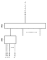
図26は、従来技術のサイクリックAWGの構成を示す平面図である。サイクリックAWG9100は、第1の入出力導波路9101、第1のスラブ導波路9102、アレイ導波路9103、第2のスラブ導波路9104および第2の入出力導波路9105が順次接続されて、構成されている。サイクリックAWG9100は、光波長合分波回路として動作する。すなわち、第1の入出力導波路9101の各導波路に、波長チャネルごとに入力した複数の信号光を、第2の入出力導波路9105に合波し、波長多重信号光として出力する機能と、第2の入出力導波路9105に入力した波長多重信号光を、第1の入出力導波路9101の各導波路へ分波し、波長チャネルごとに信号光として出力する機能を有する。
FIG. 26 is a plan view showing a configuration of a conventional cyclic AWG. The cyclic AWG 9100 includes a first input /
図26において、アレイ導波路9103の個々の導波路の長さは、一定量ΔLずつ順次長くなるよう設計されている。このとき第1の入出力導波路9101の各導波路の内の中央の導波路から第2の入出力導波路9102への透過中心波長λCは、次式で表される。
λC=naΔL/M 式(1)
In FIG. 26, the lengths of the individual waveguides of the
λ C = n a ΔL / M Formula (1)
ここで、naはアレイ導波路9101の実効屈折率であり、MはAWGの回折次数である。Mは任意の整数を取ることができるので、AWGの透過中心波長は複数存在する。ある回折次数に対応する透過中心波長(透過中心周波数)と、それとは1つ異なる回折次数に対応する透過中心波長(透過中心周波数)との差は、AWGの自由スペクトル領域(Free Spectral Range:FSR)と呼ばれている。通常、FSRは、周波数間隔(GHz)によって表される。サイクリックAWGは、このFSRの値を所望の合分波特性に適合するように選択し、複数の異なる回折次数に対応する透過波長を使用することを前提としたAWGである。
Here, n a is the effective refractive index of the
図27は、サイクリックAWGの波長合分波機能の一設計例を示した波長合分波器の概念図である。サイクリックAWGを用いた波長合分波回路9200は、第1の入出力導波路に対応する複数のポート9201、第2の入出力導波路に対応するポート9202を持つ。本例では複数のポート9201は8ポート(導波路)から構成され、各ポートの透過中心波長の間隔を100GHzとした場合を示す。FSRは800GHzになるよう設計する。ここで、波長多重信号の中に100GHz間隔で含まれる光信号の各波長をλ1、λ2、…、λ48とする。サイクリックAWGを用いた波長合分波回路9200は、複数のポート9201(第1の入出力導波路)の各ポートから入力する800GHz周期の信号光を第2の入出力導波路に合波して出力し、また逆方向に、波長多重信号光を各800GHz周期の信号光に分波して出力する機能を有する。より具体的な周波数は後述する。
FIG. 27 is a conceptual diagram of a wavelength multiplexer / demultiplexer showing one design example of the wavelength multiplexing / demultiplexing function of the cyclic AWG. A wavelength multiplexing /
図27の光合分波器9200を実現するサイクリックAWG9100は、一例として、以下の構成により実現できる。導波路のコア・クラッド間比屈折率差が1.5%、コア厚4.5μmである。第1の入出力導波路9101、アレイ導波路9103、第2の入出力導波路9105のコア幅はそれぞれ4.5μmである。アレイ導波路9103の本数は50本、導波路長差ΔLは254.2475μmである。また第1のスラブ導波路9102、第2のスラブ導波路9104の長さはいずれも1128μmである。さらに、第1のスラブ導波路9102に接続する部分の第1の入出力導波路9101の導波路間隔は15μmであり、第1のスラブ導波路9102および第2のスラブ導波路9104がそれぞれ接続する部分の、アレイ導波路9103の導波路間隔は10μmである。
As an example, the cyclic AWG 9100 that realizes the optical multiplexer /
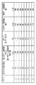
図28は、サイクリックAWGによって構成された図27の光合分波器において、合分波される各信号光の透過中心波長を対応する光周波数によって示した表である。第1の入出力導波路9101の各ポートにおいて、回折次数に対応した複数の異なる透過波長が使用される。例えば表のポート1の列を参照すると、回折次数が242の場合には周波数196400GHzが、回折次数が241の場合には195600GHzが、回折次数が240の場合には周波数194800GHzがそれぞれ対応する。ここで、1つのポートへ入力される波長多重光の各光信号を見れば、回折次数が1つ異なるとき、隣り合う2つの光周波数の周波数間隔が800GHzとなっている。すなわち、隣り合う2つの光周波数の周波数間隔はFSRに対応している。また、隣り合うポート間で周波数を見れば、100GHzずつ異なる周波数が配置されている。ポート1からポート8へ向かって、順次、100GHz間隔の周波数が配置され、ポート8の周波数に続いて、再びポート1に次の周波数が割り当てられており、周回的(サイクリック)に周波数が配置構成されていることがわかる。
FIG. 28 is a table showing the transmission center wavelength of each signal light to be multiplexed / demultiplexed by the corresponding optical frequency in the optical multiplexer / demultiplexer of FIG. 27 configured by cyclic AWG. In each port of the first input /
図28に示された各信号光の周波数は、国際標準ITU−T G.694.1勧告で定められる周波数グリッド(以下、「ITU−Tグリッド」と呼ぶ)に一致する100GHz間隔の光周波数群を有している。図27における第1のポートの波長λ1は表の最上段左端の196400GHz(波長1526.438nm)に対応し、第8のポートの波長λ48は表の最下段右端の191700GHz(波長1563.862nm)に対応する。図28に記載された周波数の範囲は、光波長多重通信の一般的な使用領域であるCバンド(波長:1530〜1565nm)に一致している。 The frequency of each signal light shown in FIG. 28 is an optical frequency group at intervals of 100 GHz that matches a frequency grid defined by the international standard ITU-T G.694.1 recommendation (hereinafter referred to as “ITU-T grid”). have. The wavelength λ 1 of the first port in FIG. 27 corresponds to 196400 GHz (wavelength 1526.438 nm) at the uppermost left end of the table, and the wavelength λ 48 of the eighth port is 191700 GHz (wavelength 1563.862 nm at the lowermost right end of the table). ). The frequency range described in FIG. 28 corresponds to the C band (wavelength: 1530 to 1565 nm), which is a general use region of optical wavelength division multiplexing communication.
図29および図30は、サイクリックAWGを実際のWDMシステムで使用する場合の構成例を示した図である。図29および図30は、異なる増設段階におけるシステム構成をそれぞれ示しており、図29が初期段階に、図30が増設後の段階に対応する。図29を参照すると、WDMシステムは6分岐のカプラ9400を持っており、カプラ9400に代えて6ポートの波長群合分波フィルタ9400とすることもできる。カプラ9400の1つのポートには、図27に示したサイクリックAWG9401が接続されている。図30は増設段階が進んだWDMシステムの状態を示しており、カプラまたはフィルタ9400の6つのポートには6つのサイクリックAWG9401〜9406が接続されている。全体では、波長多重光がそれぞれ入出力され得る48ポートを備えた、波長合分波フィルタとして機能する。
FIG. 29 and FIG. 30 are diagrams showing a configuration example when the cyclic AWG is used in an actual WDM system. FIG. 29 and FIG. 30 respectively show the system configuration at different expansion stages, with FIG. 29 corresponding to the initial stage and FIG. 30 corresponding to the stage after the expansion. Referring to FIG. 29, the WDM system includes a 6-
WDMシステムの導入にあたっては、初期の段階において、Cバンドのすべての波長の信号を運用する必要は無い。必要な波長数の光送受信装置を設置して運用を開始して、その後に伝送容量の需要に応じて波長数を増加させるのが通常である。したがって、図30のように48ポート分の波長合分波フィルタを設置するのではなく、初期段階では図29のように一部の波長数(ここでは8)に対応するサイクリックAWGだけを導入するのが好ましい。初期コストを抑えて運用を開始して、最終的には図30のようにサイクリックAWGを6つに増設して48ポートの合分波フィルタを実現するのがオペレーションコストの観点から経済的である。 In introducing the WDM system, it is not necessary to operate signals of all wavelengths in the C band in the initial stage. It is usual to install an optical transmitter / receiver having the required number of wavelengths and start operation, and then increase the number of wavelengths according to the demand for transmission capacity. Therefore, instead of installing 48-port wavelength multiplexing / demultiplexing filters as shown in FIG. 30, only cyclic AWGs corresponding to a part of the number of wavelengths (here, 8) are introduced as shown in FIG. 29 at the initial stage. It is preferable to do this. It is economical from the viewpoint of operation cost to start operation at a reduced initial cost, and finally to realize a 48-port multiplexing / demultiplexing filter by adding six cyclic AWGs as shown in FIG. is there.
またシステムの増設の際、同一種類のサイクリックAWGを利用することで、メインテナンスに必要な部品を統一し、保守用部品の種類を減らして、運用コストを下げることができる。この観点からも、Cバンド全体をカバーし得るサイクリックAWGは、別個に専用仕様で設計され異なる透過中心波長を有する非サイクリックのAWGを複数種類用いるよりも、システムの管理や保守の容易さコストの面で望ましい。 In addition, by using the same type of cyclic AWG when expanding the system, it is possible to unify the parts necessary for maintenance, reduce the types of maintenance parts, and reduce the operation cost. From this point of view, the cyclic AWG that can cover the entire C-band is easier to manage and maintain than to use multiple types of acyclic AWGs that are separately designed with special specifications and have different transmission center wavelengths. Desirable in terms of cost.
しかしながら、サイクリックAWGでは、実際に実現される透過中心波長にはITU−T等の規定されたグリッドからのずれがあり、その精度の点で通信チャネルの狭帯域化への問題となっていた。サイクリックAWGでは、使用する入出力導波路(ポート)および回折次数の組み合わせに対応するすべての透過中心波長について、実際に実現される透過中心波長が、所望の信号光の波長すなわちITU−Tクリッドで規定された波長に完全に一致するわけではない。これは、次の2つの理由による。1つは、AWGの透過中心波長とFSRが独立して定まるパラメータではないため、透過中心波長を優先して合わせこむ設計を行うと、FSRは狙いの値からずれてしまうのが通常であることによる。もう1つは、FSRの値が入出力導波路によってわずかに変化するためである。ある特定のポートに対するFSRが目標値の通りであっても、他のポートではFSRの目標値からずれてしまう。サイクリックAWGにおける原理的なグリッド波長ずれについては、非特許文献1に詳細に記載されている。
However, in the cyclic AWG, the transmission center wavelength actually realized is deviated from a specified grid such as ITU-T, which has been a problem for narrowing the communication channel in terms of accuracy. . In the cyclic AWG, for all transmission center wavelengths corresponding to combinations of input / output waveguides (ports) and diffraction orders to be used, the transmission center wavelength actually realized is the wavelength of the desired signal light, that is, the ITU-T grid. It does not exactly match the wavelength specified in. This is due to the following two reasons. The first is that the transmission center wavelength of the AWG and the FSR are not parameters that are determined independently. Therefore, if the design is made so that the transmission center wavelength is preferentially adjusted, the FSR usually deviates from the target value. by. The other is that the FSR value slightly changes depending on the input / output waveguide. Even if the FSR for a specific port is equal to the target value, the other ports deviate from the target value of the FSR.
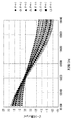
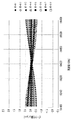
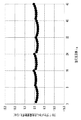
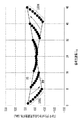
図31は、実際のサイクリックAWGにおける透過中心波長のITU−Tクリッドからのずれを説明する図である。図31において、横軸は信号光の波長λNに対応する波長(チャネル)番号Nを示しており、縦軸はITU−Tグリッドからのずれ量を光周波数で示している。図27および図28に示した透過中心波長を持つ全48チャネルの信号光について、実際に作製されたサイクリックAWGの透過中心波長は、ITU−Tグリッドの規定値から最大で±12GHz(±0.096nm)のずれが生じている。 FIG. 31 is a diagram for explaining the deviation of the transmission center wavelength from the ITU-T crid in an actual cyclic AWG. In FIG. 31, the horizontal axis indicates the wavelength (channel) number N corresponding to the wavelength λ N of the signal light, and the vertical axis indicates the amount of deviation from the ITU-T grid in terms of optical frequency. With respect to the signal light of all 48 channels having the transmission center wavelengths shown in FIGS. 27 and 28, the transmission center wavelength of the actually produced cyclic AWG is ± 12 GHz (± 0) at the maximum from the specified value of the ITU-T grid. .096 nm).
上述のサイクリックAWGにおける波長ずれの問題は、従来技術によっても、ある程度解決はできる。サイクリックAWGにおいては、環境温度による透過中心波長の変動を抑制するために、ヒータ等によってAWG回路の温度を一定に保つよう構成された、温度調整タイプのものが利用されている。図29および図30で示したようなWDMシステムにおいてサイクリックAWGを使用する場合では、各AWGにおいて使用する波長に対応する回折次数に応じて、一定に保つ設定温度を微調整して、透過中心波長のグリットずれを低減することができる。 The problem of wavelength shift in the above-mentioned cyclic AWG can be solved to some extent even by the prior art. In the cyclic AWG, in order to suppress the fluctuation of the transmission center wavelength due to the environmental temperature, a temperature adjustment type configured to keep the temperature of the AWG circuit constant by a heater or the like is used. In the case of using a cyclic AWG in the WDM system as shown in FIGS. 29 and 30, the transmission temperature is adjusted by finely adjusting the set temperature to be kept constant according to the diffraction order corresponding to the wavelength used in each AWG. Wavelength grid shift can be reduced.
例えば、図30に示した、波長番号Nが1〜8の光信号を使用するAWG9401は、図28に示したように回折次数が242に対応している。このAWG9401については、マイナスの周波数ずれ量(−5〜−13GHz:図31)を補償(相殺)する様な方向に、相対的にAWGの設定温度を調整すれば良い。同様に、波長番号Nが9〜16の光信号を使用するAWG9402は、回折次数が241に対応しており、このAWGについてはマイナスの周波数ずれ量(−4〜−8GHz)を補償(相殺)する様な方向に、相対的にAWGの設定温度を調整する。また、波長番号Nが41〜48の光信号を使用するAWG9406は、回折次数が237に対応しており、このAWGについてはプラスの周波数ずれ量(+4〜+12.5GHz)を補償(相殺)する様な方向に、相対的にAWGの設定温度を調整する。したがって、図30に示した増設後の構成のWDMシステムにおいては、6つのサイクリックAWG9401〜9406の各々に対して、使用している回折次数に応じて微調整された設定温度に、調整を行うことになる。
For example, the
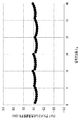
図32は、使用する回折次数に応じてAWGの温度を最適に調整した場合の、透過中心波長のITU−Tクリッドからのずれを説明する図である。温度補償を行っていない図31の周波数ずれ量と比べれば、ずれ量の絶対値はかなり抑えられているが、依然として、ずれ量の最大値は±5GHz(±0.04nm)に達している。このように、従来技術によるサイクリックAWGにおいては、実際に作製可能なAWGの透過中心波長には、ITU−Tクリッドからのずれが生じていた。 FIG. 32 is a diagram for explaining a deviation of the transmission center wavelength from the ITU-T grid when the AWG temperature is optimally adjusted according to the diffraction order to be used. The absolute value of the shift amount is considerably suppressed as compared with the frequency shift amount of FIG. 31 in which temperature compensation is not performed, but the maximum value of the shift amount still reaches ± 5 GHz (± 0.04 nm). As described above, in the cyclic AWG according to the prior art, the transmission center wavelength of the AWG that can be actually produced has deviated from the ITU-T crid.
既に述べたようにWDM技術は、例えば光透過率が高くエルビウム添加光ファイバ増幅器が適用できるCバンド(波長:1530〜1565nm)において利用されている。通信トラフィックの増大に応え、より多くの光信号を多重化するために、1つの光信号に対応するチャネル帯域幅がより狭くなってきている。近年では、従来の50GHz間隔のチャネル配置構成から25GHz間隔(チャネル帯域幅も25GHz)のチャネル配置構成への移行が進みつつある。例えば、192チャネルの光信号が25GHz間隔で配置され多重化されたWDM信号を利用するシステムが求められている。 As already described, the WDM technology is used in the C band (wavelength: 1530 to 1565 nm) where, for example, the optical transmittance is high and an erbium-doped optical fiber amplifier can be applied. In response to an increase in communication traffic, in order to multiplex more optical signals, the channel bandwidth corresponding to one optical signal has become narrower. In recent years, a transition from a conventional channel arrangement configuration with 50 GHz intervals to a channel arrangement configuration with 25 GHz intervals (channel bandwidth is also 25 GHz) is progressing. For example, there is a need for a system that uses a WDM signal in which 192-channel optical signals are arranged and multiplexed at 25 GHz intervals.
このような中で、サイクリックAWGの周波数ずれの問題は、回折次数に応じてAWG回路の動作温度を微調整しても、完全に抑制することはできていない。透過中心波長の精度を求められる狭波長チャネル間隔のWDMシステムにおいては、場合によっては要求性能を満足できない、という問題があった。 Under such circumstances, the problem of the frequency shift of the cyclic AWG cannot be completely suppressed even if the operating temperature of the AWG circuit is finely adjusted according to the diffraction order. In a WDM system with a narrow wavelength channel spacing that requires accuracy of the transmission center wavelength, there is a problem that the required performance cannot be satisfied in some cases.
本発明は、かかる問題を鑑みてなされたものであり、その目的とするところは、サイクリックAWGにおいて生じる透過中心波長(透過中心周波数)のITU−Tグリッドからのずれを補償し、全使用波長領域において透過中心波長の精度に優れた光波長合分波回路を提供することにある。 The present invention has been made in view of such a problem, and an object of the present invention is to compensate for the deviation of the transmission center wavelength (transmission center frequency) generated in the cyclic AWG from the ITU-T grid, and to use all the wavelengths used. An object of the present invention is to provide an optical wavelength multiplexing / demultiplexing circuit having excellent transmission center wavelength accuracy in the region.
本発明は、このような課題を達成するために、請求項1の発明は、所定の光路長差で順次長くなる導波路からなるアレイ導波路、前記アレイ導波路の一端に接続された第1のスラブ導波路および前記アレイ導波路の他端に接続された第2のスラブ導波路を備え、複数の回折次数に対応した透過波長を使用する波長合分波回路において、各々が干渉回路を介して前記第1のスラブ導波路に光学的に接続された複数の第1の入出力導波路と、前記第2のスラブ導波路に接続された第2の入出力導波路とをさらに備えており、前記干渉回路は、前記複数の第1の入出力導波路の各々から入力された基底モード光の一部を、1次モード光に変換する1次モード励起機構と、前記1次モード励起機構に光学的に接続し、少なくとも基底モード光および1次モード光が伝搬可能であって、前記基底モード光および前記1次モード光の間に所定の透過波長に対して所定の位相差を与えるマルチモード導波路とを有し、前記干渉回路と前記第1のスラブ導波路との接続面において形成された光フィールド分布のピーク位置が、波長によって前記マルチモード導波路の導波路幅方向に変化し、前記変化によって、前記複数の回折次数に対応した透過波長の、規格化されたグリッドからのずれを補償するよう構成されたことを特徴とする光波長合分波回路である。
In order to achieve the above object, according to the present invention, an invention according to
ここで、規格化されたグリッドは、例えば、国際標準ITU−T G.694.1勧告で定められる周波数グリッドITU−Tグリッドに対応する。また、光フィールド分布のピーク位置が変化するマルチモード導波路の導波路幅方向は、例えば、図4、図10、図15、図22におけるp軸方向に対応する。 Here, the standardized grid corresponds to, for example, the frequency grid ITU-T grid defined in the international standard ITU-T G.694.1 recommendation. Further, the waveguide width direction of the multimode waveguide in which the peak position of the optical field distribution changes corresponds to, for example, the p-axis direction in FIGS. 4, 10, 15, and 22.
請求項2の発明は、請求項1の光波長合分波回路であって、入力された光の全パワーに対して、前記1次モード励起機構において1次モード光に変換されるパワーの割合が、前記複数の第1の入出力導波路の各々の導波路で異なることを特徴とする。 A second aspect of the present invention is the optical wavelength multiplexing / demultiplexing circuit according to the first aspect, wherein the ratio of the power converted into the primary mode light in the primary mode excitation mechanism with respect to the total power of the input light Is different in each of the plurality of first input / output waveguides.
請求項3の発明は、請求項1または2の光波長合分波回路であって、前記基底モード光および前記1次モード光の間の位相差は、所定の長さを有する前記マルチモード導波路において、波長によって変化することを特徴とする。 A third aspect of the present invention is the optical wavelength multiplexing / demultiplexing circuit according to the first or second aspect, wherein a phase difference between the fundamental mode light and the first-order mode light has a predetermined length. The waveguide is characterized by changing according to the wavelength.
請求項4の発明は、請求項1乃至3いずれかの光波長合分波回路であって、前記1次モード励起機構は、光スプリッタと、前記光スプリッタに接続する第1のアーム導波路および第2のアーム導波路と、前記第1のアーム導波路および第2のアーム導波路に接続し、前記第2のアーム導波路から入力する基底モード光を1次モードに変換し、前記第1のアーム導波路から入力する基底モードと合流させて出力する光モード合成カプラで構成され、前記基底モード光および前記1次モード光の間の位相差は、前記第1のアーム導波路と第2のアーム導波路の設定された光路長差において、波長によって変化することを特徴とする。 A fourth aspect of the present invention is the optical wavelength multiplexing / demultiplexing circuit according to any one of the first to third aspects, wherein the primary mode excitation mechanism includes an optical splitter, a first arm waveguide connected to the optical splitter, and A second arm waveguide, connected to the first arm waveguide and the second arm waveguide, for converting a fundamental mode light input from the second arm waveguide into a first-order mode; And an optical mode synthesizing coupler that combines and outputs the fundamental mode input from the arm waveguide, and the phase difference between the fundamental mode light and the primary mode light is the same as that of the first arm waveguide and the second mode light. The set optical path length difference of the arm waveguide varies depending on the wavelength.
請求項5の発明は、請求項4の光波長合分波回路であって、前記光モード合成カプラは、幅の異なる2本の導波路から構成された方向性結合器であることを特徴とする。
The invention according to
請求項6の発明は、請求項1乃至3いずれかの光波長合分波回路であって、前記1次モード励起機構は、導波路コアの幅の中心軸をずらして接続した導波路オフセットであることを特徴とする。 A sixth aspect of the present invention is the optical wavelength multiplexing / demultiplexing circuit according to any one of the first to third aspects, wherein the primary mode excitation mechanism is a waveguide offset connected by shifting a central axis of the width of the waveguide core. It is characterized by being.
請求項7の発明は、請求項1乃至6いずれかの光波長合分波回路であって、前記マルチモード導波路は、テーパ導波路を介して前記第1のスラブ導波路に接続されていることを特徴とする。 A seventh aspect of the present invention is the optical wavelength multiplexing / demultiplexing circuit according to any one of the first to sixth aspects, wherein the multimode waveguide is connected to the first slab waveguide via a tapered waveguide. It is characterized by that.
以上説明したように、本発明により、サイクリックAWGタイプの光波長合分波回路において、透過中心波長のITU−Tクリッドからのずれを抑制することができる。狭波長チャネル間隔のWDMシステムに適用可能な、サイクリックAWGタイプの光波長合分波回路を実現することができる。 As described above, according to the present invention, in the cyclic AWG type optical wavelength multiplexing / demultiplexing circuit, it is possible to suppress the deviation of the transmission center wavelength from the ITU-T crid. A cyclic AWG type optical wavelength multiplexing / demultiplexing circuit applicable to a WDM system having a narrow wavelength channel interval can be realized.
従来技術のサイクリックAWGにおいては、WDMシステムで使用される複数のAWGの各々に温度調整を行って周波数ずれを補償していた。しかし、AWGで使用する波長に対応した回折次数ごとにずれ量を補正するのに留まっており、不十分なものであった。本発明では、全く異なる視点から、サイクリックAWGの少なくとも一方のスラブ導波路に接続された複数のポート(入出力導波路)に着目して、ポート毎に光フィールドの位置を調整する。スラブ導波路の接続面における、導波路幅方向の光フィールドの位置を、波長に応じて変化させる機構を持つことによって、透過中心波長の周波数ずれを大幅に減らす。光フィールドの位置の調整は、ポート毎に、2つの異なるモード光の発生量および位相差を調整することによって行われ、1つのポート内に現れる異なる光周波数の複数の光信号の透過中心波長を同時に補正することができる。以下、本発明に係るサイクリックAWGの動作原理について説明する。 In the cyclic AWG of the prior art, the frequency shift is compensated by adjusting the temperature of each of the plurality of AWGs used in the WDM system. However, it has been insufficient to correct the shift amount for each diffraction order corresponding to the wavelength used in the AWG, which is insufficient. In the present invention, from a completely different viewpoint, focusing on a plurality of ports (input / output waveguides) connected to at least one slab waveguide of the cyclic AWG, the position of the optical field is adjusted for each port. By having a mechanism for changing the position of the optical field in the waveguide width direction on the connection surface of the slab waveguide according to the wavelength, the frequency shift of the transmission center wavelength is greatly reduced. The position of the optical field is adjusted by adjusting the generation amount and phase difference of two different mode lights for each port, and the transmission center wavelengths of a plurality of optical signals having different optical frequencies appearing in one port are adjusted. It can be corrected at the same time. Hereinafter, the operation principle of the cyclic AWG according to the present invention will be described.
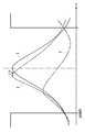
図1は、光導波路を導波する基底モード光および1次モード光の電界分布(光フィールド)を説明する概念図である。導波路上のコアを伝播する光の中には、異なる伝播モードの光が含まれ得る。図1は、サイクリックAWGの一方のスラブ導波路と、このスラブ導波路に接続される入出力導波路との間の接続部における断面を見たときの、伝播光のモードを説明している。図1の横軸は、入出力導波路の幅方向における位置を示している。横軸上で導波路端と表記した部分は、導波路コア部の両端位置に対応している。縦軸は、光フィールドの強度分布を示している。 FIG. 1 is a conceptual diagram for explaining the electric field distribution (optical field) of fundamental mode light and primary mode light guided through an optical waveguide. The light propagating through the core on the waveguide may include light of different propagation modes. FIG. 1 illustrates a mode of propagating light when a cross section at a connection portion between one slab waveguide of a cyclic AWG and an input / output waveguide connected to the slab waveguide is viewed. . The horizontal axis in FIG. 1 indicates the position in the width direction of the input / output waveguide. The portion indicated as the waveguide end on the horizontal axis corresponds to the both end positions of the waveguide core portion. The vertical axis represents the intensity distribution of the light field.
再び、図26に示した構成の従来技術のサイクリックAWG9100を参照すると、通常、複数の導波路からなる第1の入出力導波路9101の各導波路には基底モード光のみが伝播する。したがって、第1のスラブ導波路9102と、第1の入出力導波路9101の内の1つの導波路との接続部に励起される光フィールド1のピーク位置は波長によって変化せず、概ね導波路断面の中心位置(一点破線で表示)となる。ここで、上述の光フィールド1に、特定の強度比で1次モード光3が混在している場合を考える。このとき、基底モード光1および1次モード光3の干渉によって、干渉光2の光フィールドのピーク位置は導波路断面を横方向(導波路幅方向)にシフトする。
Referring again to the conventional
干渉光2の光フィールドのピーク位置の導波路幅方向におけるシフト量は、両モード光の強度比および位相差によって変化する。基底モード光および1次モード光の間の位相差が0の場合、シフト量は単純に両モード光の強度比によって決まる。一方、基底モード光および1次モード光の間に位相差を与えていくと、その位相差によって両モード光の干渉の影響が緩和される。具体的には、干渉光2の光フィールドのピーク位置の、p軸方向のシフト量は、両モード光の間の位相差が増えるに従って減少する。したがって、両モード光の位相差がπ/2の場合、シフト量は両モード光の強度比によらず0となる。
The amount of shift in the waveguide width direction of the peak position of the optical field of the
ここで、サイクリックAWGの一方のスラブ導波路に接続されるポートに注目する、一例を挙げれば、ポートは、図26の一方のスラブ導波路9101に接続される複数の導波路からなる第1の入出力導波路9101の各導波路に対応する。各ポートでは、光合分波回路によって分波または合波される光が入力または出力される。以下の説明では1つのポートは、1つの入出力導波路に対応付けて考えることができる。図26における第1の入出力導波路9101は入出力導波路が8本含まれているが、合分波特性の仕様に応じて、異なる本数の入出力導波路が含まれ得ることに留意されたい。
Here, paying attention to a port connected to one slab waveguide of the cyclic AWG, for example, the port is a first composed of a plurality of waveguides connected to one
本発明では、サイクリックAWGの各ポートを透過する、異なる波長(周波数)を持つ複数の光信号に対して、その波長(周波数)に応じて基底モード光および1次モード光の間の位相差が異なるよう入出力導波路を構成する。AWGの1つポートを透過する異なる波長を持つ複数の光信号ごと、上記基底モード光および1次モード光の間位相差を設定する。これによって、透過する光信号の波長(周波数)に応じて、第1のスラブ導波路9102に入射される光の位置を異ならせるようにすることができる。
In the present invention, for a plurality of optical signals having different wavelengths (frequencies) that pass through the respective ports of the cyclic AWG, the phase difference between the base mode light and the primary mode light according to the wavelengths (frequencies). The input / output waveguides are configured so as to be different. For each of a plurality of optical signals having different wavelengths that pass through one port of the AWG, a phase difference is set between the base mode light and the primary mode light. As a result, the position of the light incident on the
第1の入出力導波路9101の内の1つのポートに対応する導波路と、第1のスラブ導波路9102との接続部における光フィールドのピーク位置に応じて、AWGの当該ポートにおける透過中心波長は変動する。したがって、第1の入出力導波路9101において、適当な機構を備えることにより、所定の強度比の1次モード光を励起し、この1次モード光および基底モード光の間の位相差が、波長によって変化していれば良い。1次モード光および基底モード光の強度比および両者の位相差を、波長に応じて制御することができれば、従来技術によるサイクリックAWGにおいて課題となっていた、各ポートに現われる異なる波長(透過中心波長)を持つ複数の光信号の透過中心波長を同時に補正することが可能となる。
Depending on the peak position of the optical field at the connection between the waveguide corresponding to one port of the first input /
したがって、本発明の波長合分波回路(サイクリックAWG)は、所定の光路長差で順次長くなる導波路からなるアレイ導波路、前記アレイ導波路の一端に接続された第1のスラブ導波路および前記アレイ導波路の他端に接続された第2のスラブ導波路を備え、複数の回折次数に対応した透過波長を使用する波長合分波回路において、各々が干渉回路を介して前記第1のスラブ導波路に光学的に接続された複数の第1の入出力導波路と、前記第2のスラブ導波路に接続された第2の入出力導波路とをさらに備えている。 Therefore, the wavelength multiplexing / demultiplexing circuit (cyclic AWG) of the present invention includes an arrayed waveguide consisting of waveguides that become longer sequentially with a predetermined optical path length difference, and a first slab waveguide connected to one end of the arrayed waveguide. And a second slab waveguide connected to the other end of the arrayed waveguide, and a wavelength multiplexing / demultiplexing circuit using transmission wavelengths corresponding to a plurality of diffraction orders, each of which is connected to the first via an interference circuit. And a plurality of first input / output waveguides optically connected to the slab waveguide, and a second input / output waveguide connected to the second slab waveguide.
本発明の波長合分波回路の干渉回路は、前記複数の第1の入出力導波路の各々から入力された基底モード光の一部を、1次モード光に変換する1次モード励起機構と、前記1次モード励起機構に光学的に接続し、少なくとも基底モード光および1次モード光が伝搬可能であって、前記基底モード光および前記1次モード光の間に所定の透過波長に対して所定の位相差を与えるマルチモード導波路とを有し、前記干渉回路と前記第1のスラブ導波路との接続面において形成された光フィールド分布のピーク位置が、波長によって前記マルチモード導波路の導波路幅方向に変化し、前記変化によって、前記複数の回折次数に対応した透過波長の、規格化されたグリッドからのずれを補償するよう構成されている。 An interference circuit of a wavelength multiplexing / demultiplexing circuit according to the present invention includes a primary mode excitation mechanism that converts a part of the fundamental mode light input from each of the plurality of first input / output waveguides to primary mode light. , Optically connected to the first-order mode excitation mechanism, and capable of propagating at least a fundamental mode light and a first-order mode light, and having a predetermined transmission wavelength between the fundamental-mode light and the first-order mode light. A multimode waveguide that provides a predetermined phase difference, and the peak position of the optical field distribution formed on the connection surface between the interference circuit and the first slab waveguide depends on the wavelength of the multimode waveguide. It changes in the waveguide width direction, and the change is configured to compensate the deviation of the transmission wavelength corresponding to the plurality of diffraction orders from the standardized grid.
以下、具体的な実施例とともに本発明の構成および動作をさらに詳細に説明する。以下の実施例では、本発明特有の構成を持つサイクリックAWGとアサーマルAWGの構成との様々な組み合わせを含む具体的な構成と波長ずれの改善効果が示される。 Hereinafter, the configuration and operation of the present invention will be described in more detail with specific examples. In the following examples, a specific configuration including various combinations of a cyclic AWG and an athermal AWG configuration having a configuration unique to the present invention and an effect of improving wavelength shift are shown.
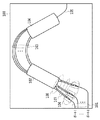
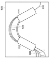
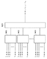
図2は、本発明の実施例1のサイクリックAWGの構成を示す平面図である。サイクリックAWG100は、従来技術のAWGと同様に、第1の入出力導波路101、第1のスラブ導波路102、アレイ導波路103、第2のスラブ導波路104、および第2の入出力導波路105を備えている。本発明のサイクリックAWG100は、第1の入出力導波路101および第1のスラブ導波路102の間に、1次モード光励起機構である導波路オフセット106、マルチモード導波路107およびテーパ導波路108をさらに備えている。
FIG. 2 is a plan view showing the configuration of the cyclic AWG according to the first embodiment of the present invention. The
したがって、サイクリックAWG100は、所定の光路長差で順次長くなる導波路からなるアレイ導波路103、前記アレイ導波路の一端に接続された第1のスラブ導波路102および前記アレイ導波路の他端に接続された第2のスラブ導波路104を備え、複数の回折次数に対応した透過波長を使用する波長合分波回路である。さらに、各々が干渉回路を介して前記第1のスラブ導波路に光学的に接続された複数の第1の入出力導波路101と、前記第2のスラブ導波路に接続された第2の入出力導波路105とをさらに備えていることになる。
Therefore, the
1次モード光励起機構である導波路オフセット106、マルチモード導波路107およびテーパ導波路108が干渉回路を構成する。すなわち、干渉回路は、前記複数の第1の入出力導波路の各々から入力された基底モード光の一部を、1次モード光に変換する1次モード励起機構と、前記1次モード励起機構に光学的に接続し、少なくとも基底モード光および1次モード光が伝搬可能であって、前記基底モード光および前記1次モード光の間に所定の透過波長に対して所定の位相差を与えるマルチモード導波路とを有しることになる。
The waveguide offset 106, the
サイクリックAWG100の各部は、以下のような構成を持つ。すべての導波路については、コア・クラッド間比屈折率差が1.5%、コア厚4.5μmである。第1の入出力導波路101、アレイ導波路103および第2の入出力導波路105のコア幅は4.5μmである。アレイ導波路103は50本の導波路を持ち、内側の導波路より一定量ΔLずつ順次長くなるよう設計され、ΔLは254.2475μmである。また第1のスラブ導波路102および第2のスラブ導波路104の長さはそれぞれ1128μmである。第1のスラブ導波路102に接続する部分の直線テーパ導波路108の配列間隔は15μmであり、第1のスラブ導波路102に接続する部分のアレイ導波路103の導波路間隔および第2のスラブ導波路104に接続する部分のアレイ導波路103の導波路間隔は、それぞれ10μmである。第1の入出力導波路101は、8本の導波路から構成されており、光合分波器としてのポート数は8である。隣接する2つのポート間の合分波光周波数間隔は100GHzで、FSRは800GHzを目標値として狙って設計されている。
Each part of the
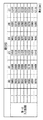
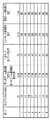
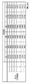
図3は、本発明のサイクリックAWGによって構成された図2の光合分波器において、合分波される各信号光の透過中心波長を対応する光周波数によって示した表である。すなわち、図3の各光周波数は、ITU−Tグリッドによって規定された光周波数であって、本発明のサイクリックAWGにおいて目標値とする光周波数が示されている。本発明のサイクリックAWGでは、実現される透過中心周波数と目標値の光周波数と間のずれ量を、従来技術とくらべて大幅に抑える。図3に示すように、第1の入出力導波路101の第1のポート(以下、ポート1と簡略化して呼ぶ)からポート8の各ポートにおいて、異なる回折次数にそれぞれ対応した複数の透過波長が使用される。サイクリックAWG100によって、表の最上段のポート1における回折次数242に対応する196400GHz(波長1526.438nm)から、表の最下段の第8のポートにおける回折次数237に対応する191700GHz(波長1563.862nm)までの48チャネルの信号光が合分波される。
FIG. 3 is a table showing the transmission center wavelength of each signal light to be multiplexed / demultiplexed by the corresponding optical frequency in the optical multiplexer / demultiplexer of FIG. 2 configured by the cyclic AWG of the present invention. That is, each optical frequency in FIG. 3 is an optical frequency defined by the ITU-T grid, and shows an optical frequency that is a target value in the cyclic AWG of the present invention. In the cyclic AWG of the present invention, the amount of deviation between the realized transmission center frequency and the optical frequency of the target value is greatly suppressed as compared with the prior art. As shown in FIG. 3, a plurality of transmission wavelengths respectively corresponding to different diffraction orders from the first port of the first input / output waveguide 101 (hereinafter simply referred to as port 1) to the
ここで1つのポートに着目すれば、異なる回折次数にそれぞれ対応した異なる光周波数の複数の光信号が合分波されることに留意されたい。例えば、ポート1では、回折次数242に対応する光周波数196400GHzから、異なる値の回折次数237に対応する光周波数192400GHzまで、6つの異なる光周波数を持つ光信号が合分波される。これらの6つの異なる光周波数の隣り合う2つは、FSRの間隔を持つ。例えば、回折次数242に対応する光周波数196400GHzと、1つ異なる値の回折次数241に対応する光周波数195600GHzとの間には、FSRに対応する800GHzの差異がある。同様のことが、ポート2からポート8までの各ポートに当てはまる。
If attention is paid to one port, it should be noted that a plurality of optical signals having different optical frequencies respectively corresponding to different diffraction orders are multiplexed / demultiplexed. For example, at
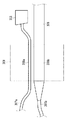
図4は、本発明の実施例1のサイクリックAWGにおける導波路オフセットから直線テーパ導波路近傍をまでの構成を拡大して示した図である。第1の入出力導波路101の内の1つのポート(入出力導波路)について示されており、構成要素の各符号は、図2に示したものと同一である。本実施例においてマルチモード導波路107は、テーパ導波路108を介して第1のスラブ導波路102に接続されている。マルチモード導波路107の導波路幅は7μmであり、直線テーパ導波路108の導波路幅は、第1のスラブ導波路102に接続する部分で11.5μmである。ここで、導波路オフセット106では、直線テーパによってマルチモード導波路107と同等までコア幅を拡大し、さらに、導波路コアの中心軸をずらしてマルチモード導波路107に接続している。導波路オフセット106のこの不連続なコア接続部において、基底モード光の一部のパワーが変換され1次モード光が励起される。
FIG. 4 is an enlarged view of the configuration from the waveguide offset to the vicinity of the linear taper waveguide in the cyclic AWG according to the first embodiment of the present invention. This is shown for one port (input / output waveguide) in the first input /
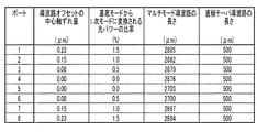
図5は、本発明の実施例1のサイクリックAWGの各ポートにおける透過中心波長の補償に関連するパラメータを示した図である。8つのポートの各ポートについて、導波路オフセット106の中心軸ずれ量(μm)、導波路オフセットにおいて基底モードから1次モードに変換される光パワーの比率(%)、マルチモード導波路107の長さ(μm)および直線テーパ導波路108の長さ(μm)の設計値を示した。
FIG. 5 is a diagram showing parameters related to the compensation of the transmission center wavelength at each port of the cyclic AWG according to the first embodiment of the present invention. For each of the eight ports, the center axis deviation amount (μm) of the waveguide offset 106, the ratio (%) of the optical power converted from the fundamental mode to the primary mode at the waveguide offset, and the length of the
本発明のサイクリックAWGでは、従来技術の構成によってAWGを作製した場合の透過中心周波数(透過中心波長)の周波数ずれ(波長ずれ量)を相殺するように、スラブ導波路の接続部における導波路幅方向の光フィールドのピーク位置を調整する。光フィールドのピーク位置は、1次モード光の発生量および位相を、相殺すべき「周波数ずれ量」に応じて設定することによって実現できる。 In the cyclic AWG of the present invention, the waveguide at the connection portion of the slab waveguide is offset so as to cancel out the frequency shift (wavelength shift amount) of the transmission center frequency (transmission center wavelength) when the AWG is manufactured by the configuration of the prior art. Adjust the peak position of the light field in the width direction. The peak position of the optical field can be realized by setting the generation amount and phase of the first-order mode light according to the “frequency shift amount” to be canceled.
したがって、本発明のサイクリックAWGでは、光フィールドのピーク位置を調整する手段として、1次モード光の発生量を制御する手段、および、1次モード光および基底モード光の間の位相差を制御する手段を備える。これらの手段を組み合わせて、1次モード光の発生量および位相を調整し、スラブ導波路の接続部における導波路幅方向の光フィールドのピーク位置を調整する。 Therefore, in the cyclic AWG of the present invention, as means for adjusting the peak position of the optical field, means for controlling the generation amount of the primary mode light, and controlling the phase difference between the primary mode light and the base mode light. Means are provided. By combining these means, the generation amount and phase of the primary mode light are adjusted, and the peak position of the optical field in the waveguide width direction at the connection portion of the slab waveguide is adjusted.
導波路オフセット106の中心軸ずれ量を大きくすると、基底モードから1次モードに変換される光パワーの比率は大きくなる。したがって、従来技術の構成によってAWGを作製した場合に透過中心周波数(透過中心波長)の周波数ずれ量(波長ずれ量)が大きなポートについては、導波路オフセット106の中心軸ずれ量を大きくすれば良い。すなわち、周波数ずれが大きいポートに対しては、導波路オフセット106の中心軸ずれ量を大きく設定すれば良い。ITU−Tグリッドは、慣習的に周波数によってチャネルを識別定義することが多いので、チャネルの透過中心波長によっても、ずれ量を表現できるが、以下の説明では、周波数ずれ量に関して説明する。ITU−Tグリッドで規定される目標値からの逸脱と言う点では、波長ずれおよび周波数ずれいずれも同一の事象を意味していることに留意されたい。 When the amount of deviation of the center axis of the waveguide offset 106 is increased, the ratio of the optical power converted from the fundamental mode to the primary mode is increased. Therefore, when the AWG is manufactured by the configuration of the prior art, the center axis deviation amount of the waveguide offset 106 may be increased for a port having a large frequency deviation amount (wavelength deviation amount) of the transmission center frequency (transmission center wavelength). . That is, for a port with a large frequency deviation, the center axis deviation amount of the waveguide offset 106 may be set large. Since the ITU-T grid customarily identifies and defines the channel by frequency, the shift amount can be expressed by the transmission center wavelength of the channel. In the following description, the frequency shift amount will be described. It should be noted that both wavelength shift and frequency shift mean the same event in terms of deviation from the target value defined by the ITU-T grid.
本実施例のサイクリックAWGは、AWGの使用温度を回折次数に応じて微調整する温度調整タイプを前提としている。すなわち、本実施例のAWGは、AWGごとに温度調整を行うことによって、透過中心周波数のずれ量を抑えるよう動作することを想定している。したがって、本発明が補償すべき周波数ずれは、図32に示したものとなる。ここで、各ポートにおいて補償すべき周波数ずれ量をより具体的に明らかにするために、ポート毎の周波数ずれ量を決定する。 The cyclic AWG of the present embodiment is premised on a temperature adjustment type in which the use temperature of the AWG is finely adjusted according to the diffraction order. That is, it is assumed that the AWG of the present embodiment operates to suppress the shift amount of the transmission center frequency by adjusting the temperature for each AWG. Therefore, the frequency deviation to be compensated by the present invention is as shown in FIG. Here, in order to clarify the frequency deviation amount to be compensated in each port more specifically, the frequency deviation amount for each port is determined.
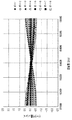
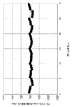
図33は、温度調整タイプのサイクリックAWGのポート毎の周波数ずれ量を説明する図である。各プロット点は、図32に示した周波数ずれの波長依存性を示したものと同一である。図33の横軸は波長番号であって、左側から右側に向かって波長番号1〜48が対応しており、縦軸は各波長番号に対して周波数ずれ量が表記されている。したがって、横軸を周波数に読み替えた場合は、右側で周波数がより低く、左側で周波数がより高くなることに注意されたい。簡単には、周波数依存特性および波長依存特性は、傾きの極性が逆になると考えれば良い。
FIG. 33 is a diagram for explaining the frequency shift amount for each port of the temperature adjustment type cyclic AWG. Each plot point is the same as that showing the wavelength dependence of the frequency shift shown in FIG. The horizontal axis in FIG. 33 is the wavelength number, and
ここで、左端の波長番号1〜8の繋がった8つのプロット点群1001は、回折次数242の波長群に対応している。同様に、右端の波長番号41〜48の繋がった8つのプロット点群1006は、回折次数237の波長群に対応している。本発明のサイクリックAWGでは、スラブ導波路の接続部における導波路幅方向の光フィールドのピーク位置を調整することによって、ポート毎に、周波数ずれを補償する。したがって、まずポート毎の周波数ずれ量を把握し、そのずれ量に応じた周波数補償を行う必要がある。
Here, the eight
図33では、ポート1に対応する波長の複数のプロット点を結んだ曲線をP1と表記している。ここで、ポート1に対応する波長は、図3の表で1と表記された列の6つの周波数(196400、195600、194800、194000、193200、192400GHz)に対応している。曲線P1が、ポート1に対応する波長に対して、補償すべき周波数ずれの周波数特性を示している。同様に、ポート8に対応する波長の複数のプロット点を結んだ曲線をP8と表記している。ここで、ポート8に対応する波長は、図3の表の8と表記された列の6つの周波数(195700、194900、194100、193300、192500、191700G)に対応している。曲線P8が、ポート8に対応する波長に対して、補償すべき周波数ずれの周波数特性を示している。図面が煩雑になるため図33には示さないが、同様にポート2〜ポート7に対応する曲線P2〜P7を想定できる。
In FIG. 33, a curve connecting a plurality of plot points of wavelengths corresponding to
このように図33から、ポート1〜ポート8のポート毎に、周波数ずれの大きさおよび周波数(波長)特性が把握できる。図33で、ポート4、ポート5(P4、P5)に着目すれば、周波数ずれは、最大でも1GHz程度で、補償が不要なレベルであることがわかる。一方で、P1およびP8の各曲線(直線)から明らかなように、ポート1およびポート8については、いずれも補償すべきずれ量の最大値は4GHzと比較的大きく、周波数ずれ量の周波数特性はその傾きが互いに逆であることが分かる。したがって、このようなポート毎に異なる周波数ずれの最大量および周波数特性(傾き・形状)に応じた補償ができれば、各々のポートに対して、ポートごとの周波数ずれ量の周波数特性に適合するように、効果的に周波数ずれを抑えることが期待できる。また、1つのポート内に現われる複数の異なる周波数に対する「補正量」の周波数特性も、図33の各プロット点から把握が可能であって、P1〜P8の各曲線に基づいて、簡単に決定できる。上述のように、本実施例では第1の入出力導波路101の内で、両端に位置しているポート1およびポート8で、周波数ずれ量が大きいことから、本発明によって補正すべき周波数ずれの「補正量」も大きくすれば良い。
As described above, the magnitude of the frequency shift and the frequency (wavelength) characteristics can be grasped for each of the
再び図5を参照すると、本実施例では、両端に位置しているポート1およびポート8において、導波路オフセット106の中心軸ずれ量をより大きくし、1次モードに変換されるパワー比を相対的に大きくする(1.5%)。また、第1の入出力導波路101の内で中央付近に位置するポート4およびポート5では、導波路オフセット106の中心軸ずれ量をゼロとしており、1次モードへ変換されるパワーが無いように設計している(0%)。このように、補償すべき周波数ずれ量の最大値に応じて、1次モード光の発生量を導波路オフセット106の中心軸ずれ量で制御している。
Referring to FIG. 5 again, in this embodiment, in the
したがって、本発明のサイクリックAWGでは、入力された光の全パワーに対して、1次モード励起機構(すなわち導波路オフセット106)において1次モード光に変換されるパワーの割合が、前記複数の第1の入出力導波路101の各々の導波路で異なることになる。
Therefore, in the cyclic AWG according to the present invention, the ratio of the power converted into the first-order mode light in the first-order mode excitation mechanism (that is, the waveguide offset 106) with respect to the total power of the input light is the plurality of the plurality of powers. The first input /
本発明のサイクリックAWGは、さらに以下のように構成される。第1の入出力導波路101の各ポートでは、導波路オフセット106において一部の光パワーが1次モードに変換される。基底モード光および1次モード光は、ともに直線テーパ導波路108と第1のスラブ導波路102の接続点に到達する。このとき、マルチモード導波路107および直線テーパ導波路108を伝搬して生じる、基底モードの光に対する実効屈折率と1次モードの光に対する実効屈折率との差分は、波長(周波数)によって異なる。このため、マルチモード導波路107および直線テーパ導波路108を通過した後の、基底モード光および1次モード光の間の位相差も波長(周波数)によって変化することになる。したがって、直線テーパ導波路108の終端(接続部)における光フィールドの分布についても、そのピーク位置は波長(周波数)によって変化することになる。したがって、基底モード光および1次モード光の間の位相差は、所定の長さを有するマルチモード導波路107において、波長によって変化することになる。
The cyclic AWG of the present invention is further configured as follows. At each port of the first input /
言い換えれば、光フィールドの分布のピーク位置は、波長(周波数)依存特性を持つ。逆にこれを利用すれば、マルチモード導波路107および直線テーパ導波路108の長さを変化させることによって、光フィールドの分布のピーク位置の波長(周波数)依存特性を制御できる。
In other words, the peak position of the optical field distribution has wavelength (frequency) dependent characteristics. Conversely, if this is utilized, the wavelength (frequency) dependence characteristics of the peak position of the distribution of the optical field can be controlled by changing the lengths of the
そこで、各ポートに対して、そのポートを透過する複数の光波(信号)の各周波数における周波数ずれ量に適合するように、すなわち、周波数ずれ量の周波数依存特性(波長依存特性)に適合するように、マルチモード導波路107とテーパ導波路108の長さを決定してやれば良い。上記の決定された長さによって、所定の波長(周波数)に対して基底モード光および1次モード光の間に「所定の位相差」が与えられる。このとき、「所定の位相差」によって、透過周中心波数のずれ量を補正する補正量の周波数(波長)特性(傾き・形状)が決定されていることになる。図33とともに説明したように、ポート1〜ポート8のポート毎に、周波数ずれの大きさおよび周波数(波長)特性(傾き・形状)が把握されている。したがって、「所定の位相差」を与えて周波数ずれの補償量の周波数(波長)特性(傾き・形状)を決定することで、図33から把握されるP1〜P8の周波数ずれの周波数(波長)特性に適合させることができる。
Therefore, for each port, the frequency deviation amount at each frequency of a plurality of light waves (signals) transmitted through the port is adapted, that is, the frequency dependence characteristic (wavelength dependence characteristic) of the frequency deviation amount is adapted. In addition, the lengths of the
したがって、マルチモード導波路107およびテーパ導波路108の長さは、1次モード光と基底モード光との間の位相差を制御する手段として機能するとともに、周波数ずれの周波数(波長)特性に適合するように、補正量の周波数特性(傾き・形状)を決定するように機能することになる。本発明のこの機能によって、直線テーパ導波路108の終端での光フィールドのピーク位置のシフト量(導波路幅方向:p軸)にしたがって、周波数ずれが補正され、かつ、あるポートを透過する、異なる周波数の複数の光波(信号)に対して、周波数ずれ量の周波数特性に適合するように、複数の透過中心波長を同時に一括して補正することができる。
Therefore, the lengths of the
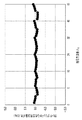
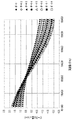
図6は、本実施例における、直線テーパ導波路終端の光フィールド分布のピーク位置が、伝搬する光波の周波数により変化する様子をポートごとに示した図である。ここで縦軸のピーク位置p(μm)は、図4におけるp座標軸の位置に対応し、p=0は直線テーパ導波路の中心位置となる。横軸は光波の周波数であって、波長番号1〜48の範囲の周波数に対応する。既に述べたように、縦軸の光フィールド分布のピーク位置のシフトによって透過中心周波数を変更し補正することができる。したがって、図6の縦軸は、周波数ずれの「補正量」を意味する。ここで、図33とともに説明した、ポート1〜ポート8のポート毎の周波数ずれの大きさおよび周波数(波長)特性と、図6に示した補正量の大きさおよび周波数特性とが対応している点に留意されたい。
FIG. 6 is a diagram showing, for each port, how the peak position of the optical field distribution at the end of the linear taper waveguide changes according to the frequency of the propagating light wave in this embodiment. Here, the peak position p (μm) on the vertical axis corresponds to the position of the p coordinate axis in FIG. 4, and p = 0 is the center position of the linear taper waveguide. The horizontal axis represents the frequency of the light wave and corresponds to the frequency in the range of
例えば、ポート1およびポート8では、図33で説明したP1およびP8の周波数ずれ量を相殺するように、図6のポート1およびポート8の補正量の大きさおよび周波数特性が設定されている。すなわち、概ね横軸の中央付近(194000GHz)でピーク位置が0(補正量が0)となり、横軸の両端で補正量が最大となるようにポート1およびポート8の補正量が設定されている。これは、図33のP1およびP8で示される周波数ずれ量が、横軸の中央付近の波長番号24付近で0であり、両端において最大となっていることに対応している。また、図6のポート1およびポート8の補正量は、その周波数特性の傾きが逆となっている。これも、図33のP1およびP8の周波数ずれ量の傾きが逆になっていることと対応している。
For example, in
また、ポート4およびポート5に着目すると。図5に示したように導波路オフセットの中心軸ずれ量が0μmに設定されているので、図6に示した補正量は0となる。これは、図33に示した曲線P4およびP5において、周波数ずれ量がほとんどなく、補正が不要であることに対応している。図6の各ポートにおける補正量の最大値および補正量の傾きの大きさは、図5に示した導波路オフセットの中心軸ずれ量に対応している。これは、例えば図5に示したポート1〜ポート4における導波路オフセットの中心軸ずれ量と、図6に示した補正量特性を対比すれば、明らかである。
Focus on
さらに、図5に示したマルチモード導波路の長さが、ポート1〜ポート4の第1グループと、ポート5〜ポート8の第2グループとの間で、173μmの不連続があることに留意されたい。図6に示した周波数ずれ「補正量」のカーブはいずれも、サイン関数状の形状を持っており2つのグループ間で、その位相が反転していることに注目されたい。上記2つのグループの間のマルチモード導波路の長さの不連続は、「補正量」のカーブの位相の反転を意味しており、図6における補正量の傾斜が正負逆転していることに対応する。
Furthermore, it is noted that the multimode waveguide shown in FIG. 5 has a discontinuity of 173 μm between the first group of
上述のように、本発明のサイクリックAWGにおける直線テーパ導波路終端の光フィールドのピーク位置の変化によって、従来のサイクリックAWGが持っていた透過中心周波数のずれが補正されることになる。この補正は、ポートごとに、導波路オフセット106の中心軸ずれ量を設定して、1次モード光の発生量を制御して行われる。またその補正量は、周波数によって変化し、1つのポート内に現れる異なる複数の周波数の光波に対して、周波数ずれ量の周波数特性に適合するように、複数の透過中心波長を同時に一括して補正することができる。 As described above, the shift of the transmission center frequency of the conventional cyclic AWG is corrected by the change in the peak position of the optical field at the end of the linear taper waveguide in the cyclic AWG of the present invention. This correction is performed by setting the center axis deviation amount of the waveguide offset 106 for each port and controlling the generation amount of the primary mode light. In addition, the amount of correction varies depending on the frequency, and multiple transmission center wavelengths are corrected simultaneously for a plurality of light waves of different frequencies appearing in one port so as to match the frequency characteristics of the frequency deviation amount. can do.
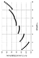
図7は、本実施例のサイクリックAWGについて、透過中心波長のITU-Tクリッドからのずれ量を示す図である。本実施例のサイクリックAWGは温度調整タイプであり、使用する回折次数によって一定に保つ温度を微調整している。本実施例のサイクリックAWGにおけるITU−Tクリッドからからの周波数ずれは、最大でも±1.2GHz(±0.010nm)であり、従来のサイクリックAWG(図32)と比較して、周波数ずれ量が約1/5に低減されている。透過中心周波数(波長)がよりITU−Tクリッドに整合したサイクリックAWGが実現されている。 FIG. 7 is a diagram showing a deviation amount of the transmission center wavelength from the ITU-T cluded for the cyclic AWG of the present embodiment. The cyclic AWG of this embodiment is a temperature adjustment type, and finely adjusts the temperature to be kept constant according to the diffraction order used. In the cyclic AWG of the present embodiment, the maximum frequency deviation from the ITU-T crid is ± 1.2 GHz (± 0.010 nm), which is a frequency deviation compared to the conventional cyclic AWG (FIG. 32). The amount is reduced to about 1/5. A cyclic AWG in which the transmission center frequency (wavelength) is more matched to the ITU-T grid is realized.
なお、本実施形態で説明したサイクリックAWGの各ポートの設計値(図5)では、ポート4およびポート5は導波路オフセットの軸ずれを持たせておらず、1次モードも励起されていない。このように1次モードを励起させる必要のないポート、すなわちITU−Tグリッドからの周波数ずれを補償する必要のないポートについては、当然のことながら、導波路オフセット106、マルチモード導波路107、直線テーパ導波路108を設ける必要はない。これらのポートは、第1の入出力導波路101と第1のスラブ導波路102とを直接接続するようにしても良い。後述する他の実施例においても同様である。
In addition, in the design value (FIG. 5) of each port of the cyclic AWG described in the present embodiment, the
本実施例のサイクリックAWGは、AWGの使用温度を回折次数に応じて微調整する温度調整タイプであった。本発明は、次の実施例で説明するように、アサーマル化された非温度調整タイプのサイクリックAWGにも適用できる。 The cyclic AWG of this example was a temperature adjustment type that finely adjusts the use temperature of the AWG according to the diffraction order. The present invention can also be applied to an athermalized non-temperature control type cyclic AWG, as will be described in the next embodiment.
本発明の実施例2に係る光波長合分波回路は、アサーマル化したサイクリックAWGに対して、実施例1で説明した本発明に特有の構成を適用したものである。本実施例のサイクリックAWGでは、AWGごとに温度調整をする必要がない。周波数ずれの補償量は、実施例1に比べて大きくなる。以下、詳細に本実施例のサイクリックAWGの構成および動作を説明する。 The optical wavelength multiplexing / demultiplexing circuit according to the second embodiment of the present invention is obtained by applying the configuration unique to the present invention described in the first embodiment to the athermalized cyclic AWG. In the cyclic AWG of the present embodiment, it is not necessary to adjust the temperature for each AWG. The amount of compensation for frequency deviation is larger than that in the first embodiment. Hereinafter, the configuration and operation of the cyclic AWG of this embodiment will be described in detail.
図8は、本発明の実施例2のサイクリックAWGの構成を示す平面図である。サイクリックAWG200は、従来技術のAWGと同様に、第1の入出力導波路201、第1のスラブ導波路202、アレイ導波路203、第2のスラブ導波路204、および第2の入出力導波路205を備えている。本発明のサイクリックAWG200は、第1の入出力導波路101および第1のスラブ導波路202の間に、1次モード光励起機構である導波路オフセット206、マルチモード導波路207および直線テーパ導波路208をさらに備えている。本実施例のサイクリックAWG200においては、温度調整を不要とするために、第1のスラブ導波路202の途中に、導波路を分断する溝209が形成され、溝209内にはシリコーン樹脂が充填されている。この溝209によって、アサーマルサイクリックAWGを実現する。
FIG. 8 is a plan view showing the configuration of the cyclic AWG according to the second embodiment of the present invention. The
図9は、本実施例のアサーマルサイクリックAWGにおいて、溝を横切る断面の構成を示す図である。図9は、図8の第1のスラブ導波路202内の線分AA´部分の断面構造を拡大して示している。図9においてスラブ導波路202は、シリコン基板210上に構成されており、導波路コア211およびクラッド212を含む。複数の溝209は、導波路コア211およびクラッド211の一部を取り除いて形成され、導波路コア211を分断している。
FIG. 9 is a diagram showing a cross-sectional configuration across the groove in the athermal cyclic AWG of the present embodiment. FIG. 9 shows an enlarged cross-sectional structure of the line segment AA ′ in the
アサーマルサイクリックAWG200の各部の構成パラメータは、以下のような構成を持つ。すべての導波路については、コア・クラッド間比屈折率差が1.5%、コア厚4.5μmである。第1の入出力導波路201、アレイ導波路203および第2の入出力導波路205のコア幅は4.5μmである。アレイ導波路203は50本の導波路を持ち、内側の導波路より一定量ΔLずつ順次長くなるよう設計され、ΔLは254.5987μmである。
The configuration parameters of each part of the athermal
図9に示したように、溝209は複数の溝に分割されている。これは、複数の溝を構成する場合のほうが、単一の溝で構成する場合と比べて、放射損失をより低減することができるからである。アレイ導波路203では、各々の導波路が一定量ΔL順次長くなるよう設計されている。すなわち、隣り合う2つの導波路の導波路長の差がΔLとなっている。第1のスラブ導波路202において複数の溝209によって分断される長さの和は、アレイ導波路203の各導波路長に応じて、各導波路に入力する光波が、ΔLに比例した量のΔL´順次長くなるような形状をしている。
As shown in FIG. 9, the
ここでαをアレイ導波路およびスラブ導波路の実効屈折率nの温度係数(α=dn/dT、Tは温度)、α´を溝に挿入された温度補償材料の屈折率n´の温度係数(α´=dn´/dT)とする。このとき、本実施例のサイクリックAWGでは、ΔL´=ΔL/(1−α´/α)の関係を満たすように設計されている。これにより、アレイ導波路およびスラブ導波路での光路長差の温度変化が、温度補償材料の光路長差の温度変化によって相殺され、透過中心波長の温度依存性が補償されている。温度補償材料としては、特にα´がαと異符号であり、かつ|α´|が|α|に比較して十分大きいような材料が好ましい。このような条件の材料としては、本実施例で適用されている光学樹脂であるシリコーン樹脂があり、α´はおよそ−35×αである。 Where α is the temperature coefficient of the effective refractive index n of the arrayed waveguide and slab waveguide (α = dn / dT, T is the temperature), and α ′ is the temperature coefficient of the refractive index n ′ of the temperature compensation material inserted in the groove. (Α ′ = dn ′ / dT). At this time, the cyclic AWG of the present embodiment is designed to satisfy the relationship ΔL ′ = ΔL / (1−α ′ / α). Thereby, the temperature change of the optical path length difference in the arrayed waveguide and the slab waveguide is offset by the temperature change of the optical path length difference of the temperature compensation material, and the temperature dependence of the transmission center wavelength is compensated. As the temperature compensation material, a material in which α ′ has a different sign from α and | α ′ | is sufficiently larger than | α | is particularly preferable. As a material under such conditions, there is a silicone resin which is an optical resin applied in this embodiment, and α ′ is approximately −35 × α.
第1のスラブ導波路202および第2のスラブ導波路204の長さは、それぞれ1128μmである。第1のスラブ導波路202に接続する部分の直線テーパ導波路208の配列間隔は15μmであり、第1のスラブ導波路202に接続する部分のアレイ導波路203の導波路間隔および第2のスラブ導波路204に接続する部分のアレイ導波路203の導波路間隔は、それぞれ10μmである。第1の入出力導波路201は、8本の導波路から構成されており、光合分波器としてのポート数は8である。隣接する2つのポート間の合分波光周波数間隔は100GHzで、FSRは800GHzを目標値として狙って設計されている。
The lengths of the
本実施例のアサーマルサイクリックAWGによって合分波される信号光の各光周波数は実施例1と同様であり、図2で表したものである。第1の入出力導波路201のポート1からポート8において、回折次数に対応した複数の透過波長が使用され、196400GHz(波長1526.438nm)から191700GHz(波長1563.862nm)までの48チャネルの信号光が合分波される。
Each optical frequency of the signal light multiplexed / demultiplexed by the athermal cyclic AWG of the present embodiment is the same as that of the first embodiment and is shown in FIG. A plurality of transmission wavelengths corresponding to the diffraction orders are used in
図10は、実施例2のサイクリックAWGにおける導波路オフセットから直線テーパ導波路近傍をまでを拡大した図である。実施例1で図8に示した構成と同様である。第1の入出力導波路101の内の1つのポート(入出力導波路)について示されており、構成要素の各符号は、図8に示したものと同一である。本実施例においてマルチモード導波路207は、テーパ導波路208を介して第1のスラブ導波路202に接続されている。マルチモード導波路207の導波路幅は7μmであり、直線テーパ導波路208の導波路幅は、第1のスラブ導波路202に接続する部分で11.5μmである。ここで、導波路オフセット206では、直線テーパによってマルチモード導波路207と同等までコア幅を拡大し、さらに、導波路コアの中心軸をずらしてマルチモード導波路207に接続している。導波路オフセット206のこの不連続なコア接続部において、基底モード光の一部のパワーが変換され1次モード光が励起される。
FIG. 10 is an enlarged view from the waveguide offset to the vicinity of the linear taper waveguide in the cyclic AWG of the second embodiment. The configuration is the same as that shown in FIG. This is shown for one port (input / output waveguide) in the first input /
図11は、本発明の実施例2のサイクリックAWGの各ポートにおける透過中心波長の補償に関連するパラメータ値を示した図である。8つのポートの各ポートについて、導波路オフセット206の中心軸ずれ量(μm)、導波路オフセットにおいて基底モードから1次モードに変換される光パワーの比率(%)、マルチモード導波路207の長さ(μm)および直線テーパ導波路208の長さ(μm)の設計値を示した。
FIG. 11 is a diagram illustrating parameter values related to transmission center wavelength compensation at each port of the cyclic AWG according to the second embodiment of the present invention. For each of the eight ports, the center axis deviation amount (μm) of the waveguide offset 206, the ratio (%) of the optical power converted from the fundamental mode to the primary mode at the waveguide offset, the length of the
本発明のアサーマル化したサイクリックAWGでも、従来技術の構成によってAWGを作製した場合の透過中心周波数(透過中心波長)の周波数ずれ(波長ずれ量)を相殺するように、スラブ導波路との接続部における導波路幅方向(p軸)の光フィールドのピーク位置を調整する。光フィールドのピーク位置は、1次モード光の発生量および位相を、相殺すべき「ずれ量」に応じて設定することによって実現できる。 Even in the athermalized cyclic AWG of the present invention, the connection with the slab waveguide so as to cancel out the frequency shift (wavelength shift amount) of the transmission center frequency (transmission center wavelength) when the AWG is manufactured by the configuration of the prior art. The peak position of the optical field in the waveguide width direction (p-axis) is adjusted. The peak position of the optical field can be realized by setting the generation amount and phase of the first-order mode light according to the “deviation amount” to be canceled.
本発明のアサーマル化したサイクリックAWGでも、光フィールドのピーク位置を調整する手段として、1次モード光の発生量を制御する手段、および、1次モード光と基底モード光との間の位相差を制御する手段を備える。これらの手段を組み合わせて、1次モード光の発生量および位相を調整し、スラブ導波路との接続部における導波路幅方向の光フィールドのピーク位置を調整する。 Even in the athermalized cyclic AWG of the present invention, as means for adjusting the peak position of the optical field, means for controlling the generation amount of the primary mode light, and the phase difference between the primary mode light and the base mode light Means for controlling. By combining these means, the generation amount and phase of the primary mode light are adjusted, and the peak position of the optical field in the waveguide width direction at the connection portion with the slab waveguide is adjusted.
実施例1と異なり、本実施例のサイクリックAWGは、アサーマル化されているのでAWGの使用温度の微調整は行わない非温度調整タイプを前提としている。したがって、本実施例のサイクリックAWGが補償すべき周波数ずれ量は、図31に示したものとなる。図32で示した実施例1で補償すべき周波数ずれ量と場合と比べて、ずれ量の大きさおよび周波数依存特性(波長依存特性)が大きく異なっている。したがって、実施例1とは異なる設定によって、光フィールドのピーク位置の調整を行うことになる。ここで、実施例1と同様に、各ポートにおいて補償すべき周波数ずれ量をより具体的に明らかにするために、ポート毎の周波数ずれ量を決定する。 Unlike the first embodiment, the cyclic AWG of the present embodiment is presumed to be a non-temperature adjustment type in which fine adjustment of the working temperature of the AWG is not performed because it is athermalized. Therefore, the amount of frequency deviation to be compensated for by the cyclic AWG of this embodiment is as shown in FIG. Compared with the case of the frequency deviation amount to be compensated in the first embodiment shown in FIG. 32, the magnitude of the deviation amount and the frequency dependence characteristics (wavelength dependence characteristics) are greatly different. Therefore, the peak position of the optical field is adjusted by a setting different from that in the first embodiment. Here, as in the first embodiment, the frequency shift amount for each port is determined in order to more specifically clarify the frequency shift amount to be compensated at each port.
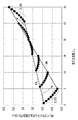
図34は、アサーマル化されたサイクリックAWGのポート毎の周波数ずれ量を説明する図である。各プロット点は、図31に示した周波数ずれの波長依存性を示したものと同一である。図34の横軸は波長番号であって、左側から右側に向かって波長番号1〜48が対応しており、縦軸は各波長番号(波長)に対して透過中心周波数の周波数ずれ量が表記されている。したがって、横軸を周波数に読み替えた場合は、横軸の右側で周波数がより低く、左側で周波数がより高くなることに注意されたい。簡単には、周波数依存特性および波長依存特性は、傾きの極性が逆になると考えれば良い。
FIG. 34 is a diagram for explaining a frequency shift amount for each port of the athermalized cyclic AWG. Each plot point is the same as that showing the wavelength dependence of the frequency shift shown in FIG. The horizontal axis in FIG. 34 is the wavelength number, and
左端の波長番号1〜8に対応する繋がった8つのプロット点群1101は、回折次数242の波長群に対応している。同様に、右端の波長番号41〜48に対応する繋がった8つのプロット点群1106は、回折次数237の波長群に対応している。本発明のアサーマル化したサイクリックAWGでも、スラブ導波路の接続部における導波路幅方向の光フィールドのピーク位置を調整することによって、ポート毎に、周波数ずれを補償する。したがって、まずポート毎の周波数ずれ量を把握し、そのずれ量に応じた周波数補償を行う必要がある。
The connected eight
図34では、ポート1に対応する波長の複数のプロット点を結んだ曲線をP1と表記している。ここで、ポート1に対応する波長は、図3の表で1と表記された列の6つの周波数(196400、195600、194800、194000、193200、192400GHz)に対応している。曲線P1が、ポート1に対応する波長に対して、補償すべき周波数ずれの周波数特性を示している。同様に、ポート8に対応する波長の複数のプロット点を結んだ曲線をP8と表記している。ここで、ポート8に対応する波長は、図3の表の8と表記された列の6つの周波数(195700、194900、194100、193300、192500、191700G)に対応している。曲線P8が、ポート8に対応する波長に対して、補償すべき周波数ずれの周波数特性を示している。図34には示さないが、同様にポート2〜ポート7に対して、曲線P2〜P7を想定できる。
In FIG. 34, a curve connecting a plurality of plot points of wavelengths corresponding to
このように図34から、ポート1〜ポート8のポート毎に、周波数ずれの大きさおよび周波数(波長)特性が把握できる。図34からは、ポート1に比べて、ポート8のほうが周波数のずれ量の最大値が大きいことがわかる。また、周波数すれ量が0となる波長(光周波数)は、ポート1からポート8にかけて、長波長側にシフトしていることも分かる。したがって、このようなポート毎に異なる周波数ずれの最大量および周波数特性(傾き・形状)に応じた補償をすることで、実施例1の場合と同様に、各々のポートに対して、ポートごとの周波数ずれ量の周波数特性に適合するように、効果的に周波数ずれを抑えることができる。1つのポート内に現われる複数の異なる周波数に対する「補正量」の周波数特性も、図34の各プロット点から把握できるP1〜P8の各曲線に基づいて、簡単に決定できる。
Thus, from FIG. 34, the magnitude of frequency deviation and frequency (wavelength) characteristics can be grasped for each of the
再び図11を参照すると、本実施例では、ポート1からポート8にかけてポート番号が大きいほど、導波路オフセット206の中心軸ずれ量を順次大きくし、1次モードに変換されるパワー比を相対的に大きくしている(2.5%から6.0%へ)。このように、補償すべき周波数ずれ量の最大値に応じて、1次モード光の発生量を導波路オフセット206の中心軸ずれ量で制御している。
Referring to FIG. 11 again, in this embodiment, as the port number increases from
本発明のアサーマル化されたサイクリックAWGは、実施例1と同様にさらに以下のように、マルチモード導波路207および直線テーパ導波路208の長さを変化させることによって、光フィールドの分布のピーク位置の波長(周波数)依存特性を制御している。 そこで、各ポートに対して、そのポートを透過する複数の光波(信号)の各周波数における周波数ずれ量に適合するように、すなわち、周波数ずれ量の周波数依存特性(波長依存特性)に適合するように、マルチモード導波路207とテーパ導波路208の長さを決定してやれば良い。
As in the first embodiment, the athermalized cyclic AWG according to the present invention further changes the lengths of the
上記の決定された長さによって、所定の周波数(波長)に対して、基底モード光および1次モード光の間に「所定の位相差」が与えられる。このとき、「所定の位相差」によって、透過周中心波数のずれ量を補正する補正量の周波数(波長)特性(傾き・形状)が決定されていることになる。図34とともに説明したように、ポート1〜ポート8のポート毎に、周波数ずれの大きさおよび周波数(波長)特性(傾き・形状)が把握されている。したがって、「所定の位相差」を与えて周波数ずれの補償量の周波数(波長)特性(傾き・形状)を決定することで、図34から把握されるP1〜P8の周波数ずれの周波数(波長)特性に適合させることができる。
With the determined length, a “predetermined phase difference” is provided between the base mode light and the first-order mode light for a predetermined frequency (wavelength). At this time, the frequency (wavelength) characteristic (inclination / shape) of the correction amount for correcting the shift amount of the transmission peripheral center wave number is determined by the “predetermined phase difference”. As described with reference to FIG. 34, the magnitude of frequency deviation and frequency (wavelength) characteristics (inclination / shape) are grasped for each of the
図34からは、周波数ずれ量が0となる波長(周波数)がポートによって少しずつ波長番号が大きい方向に変動していることが分かる。したがって、ポート毎に、周波数ずれ量が0となる波長(周波数)に適合するように、マルチモード導波路207およびテーパ導波路208の長さを決定してやれば良い。本実施例では図11に示したように、マルチモード導波路206の長さをポート1からポート8に向かって、順次短くしていくことによって、後述するように周波数ずれの補正量のカーブ(サイン関数)の位相を調整している。
From FIG. 34, it can be seen that the wavelength (frequency) at which the frequency deviation amount becomes 0 varies little by little in the direction in which the wavelength number is larger depending on the port. Therefore, the lengths of the
図12は、本実施例における、直線テーパ導波路終端の光フィールド分布ピーク位置の、伝搬する光波の周波数による変化をポート毎に示した図である。ここで縦軸のピーク位置p(μm)は、図10におけるp座標軸の位置に対応し、p=0は直線テーパ導波路の中心位置となる。横軸は光波の周波数であって、波長番号1〜48の範囲の周波数に対応する。既に述べたように、縦軸の光フィールド分布のピーク位置のシフトによって透過中心周波数を変更し補正することができる。したがって、図12の縦軸は、周波数ずれの「補正量」を意味する。
FIG. 12 is a diagram showing the change of the peak position of the optical field distribution at the end of the linear taper waveguide according to the frequency according to the frequency of the propagating light wave in this embodiment. Here, the peak position p (μm) on the vertical axis corresponds to the position of the p coordinate axis in FIG. 10, and p = 0 is the center position of the linear taper waveguide. The horizontal axis represents the frequency of the light wave and corresponds to the frequency in the range of
実施例1の場合と同様に、図34とともに説明した、ポート1〜ポート8のポート毎の周波数ずれの大きさおよび周波数(波長)特性と、図12に示した「補正量」の大きさおよび周波数特性が対応している点に留意されたい。すなわち、図34で示したP1〜P8の周波数ずれ量の特性と、図12に示した各ポートの周波数ずれの「補正量」の特性とは、相互に逆特性となっている。例えば、図12の周波数ずれ補正量の振幅(最大値)は、図34の周波数ずれ量の最大値と対応している。そして、各ポートの周波数ずれの補正量の振幅は、図11における導波路オフセット206の中心軸ずれ量と対応している。また、図12の周波数ずれ補正量が0の位置は、図34の周波数ずれ量が0の位置と対応している。そして、各ポートの周波数ずれ補正量が0の位置は、図11におけるマルチモード導波路207の長さによって制御(設定)されている。
Similarly to the case of the first embodiment, the magnitude and frequency (wavelength) characteristics of the frequency deviation for each port of the
実施例1の図6および実施例の図12における、周波数ずれの補正量のカーブは、より広い周波数範囲で示せば、サイン関数状の特性となる。そして、導波路オフセット206の中心軸ずれ量は、このサイン関数状の特性の最大振幅を決定していると考えることができる。また、マルチモード導波路207およびテーパ導波路208の長さが、サイン関数状の特性の位相を決定していると考えることができる。
The frequency deviation correction amount curves in FIG. 6 of the first embodiment and FIG. 12 of the first embodiment have a sine function characteristic if shown in a wider frequency range. The amount of deviation of the central axis of the waveguide offset 206 can be considered to determine the maximum amplitude of the sine function characteristic. In addition, it can be considered that the lengths of the
実施例1および実施例2のサイクリックAWGでは、光フィールドのピーク位置を調整する手段として、1次モード光の発生量を制御する手段が導波路オフセットに対応することになる。また1次モード光と基底モード光との間の位相差を制御(設定)する手段がマルチモード導波路207およびテーパ導波路208の長さに対応することになる。これらの手段を組み合わせて、1次モード光の発生量および位相を調整し、スラブ導波路の接続部における導波路幅方向の光フィールドのピーク位置を調整する。このように、本実施例のアサーマル化したサイクリックAWGにおける直線テーパ導波路終端の光フィールドのピーク位置の変化によって、従来のサイクリックAWGが持っていた透過中心周波数のずれは、補正されることになる。
In the cyclic AWGs according to the first and second embodiments, the means for controlling the generation amount of the first-order mode light as a means for adjusting the peak position of the optical field corresponds to the waveguide offset. The means for controlling (setting) the phase difference between the primary mode light and the fundamental mode light corresponds to the lengths of the
透過中心周波数のずれの補正は、ポートごとに、導波路オフセット106の中心軸ずれ量を設定して、1次モード光の発生量を制御して行われる。またその補正量は、周波数によって変化し、1つのポート内に現れる異なる複数の周波数の光波に対して、周波数ずれ量の周波数特性に適合するように、複数の透過中心波長を同時に一括して補正することができる。すなわち、1つのポート内に現れる異なる複数の周波数の光波に対して、周波数ずれ補正量は周波数によって変化している。 The correction of the transmission center frequency deviation is performed by setting the amount of deviation of the central axis of the waveguide offset 106 for each port and controlling the generation amount of the primary mode light. In addition, the amount of correction varies depending on the frequency, and multiple transmission center wavelengths are corrected simultaneously for a plurality of light waves of different frequencies appearing in one port so as to match the frequency characteristics of the frequency deviation amount. can do. That is, the frequency deviation correction amount varies depending on the frequency for light waves having different frequencies appearing in one port.
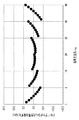
図13は、実施例2のサイクリックAWGについて、透過中心波長のITU−Tクリッドからのずれ量を示す図である。本実施例のサイクリックAWGはアサーマル化されており、非温度調整タイプであって、AWGの温度調節は行われない。本実施例のサイクリックAWGにおけるITU−Tクリッドからからの周波数ずれは、最大でも±1.7GHz(±0.014nm)であり、従来のサイクリックAWGでアサーマル化を前提とした場合(図31)に比較して、周波数ずれ量が約1/5に低減されている。透過中心周波数(波長)がよりITU−Tクリッドに整合したサイクリックAWGが実現されている。 FIG. 13 is a diagram illustrating the amount of deviation of the transmission center wavelength from the ITU-T clid for the cyclic AWG of the second embodiment. The cyclic AWG of the present embodiment is athermalized, is a non-temperature adjustment type, and the temperature of the AWG is not adjusted. In the cyclic AWG of this embodiment, the frequency deviation from the ITU-T clad is ± 1.7 GHz (± 0.014 nm) at the maximum, and when the conventional cyclic AWG is assumed to be athermal (FIG. 31). ), The frequency shift amount is reduced to about 1/5. A cyclic AWG in which the transmission center frequency (wavelength) is more matched to the ITU-T grid is realized.
なお、本実施例では、温度調整を不要とするための溝209を第1のスラブ導波路202中に設けるようにしたが、例えば、第2のスラブ導波路204やアレイ導波路203上に複数の溝209を設け、シリコーン樹脂を充填する構成にしても良いことは言うまでもない。
In this embodiment, the
上述の実施例1および実施例2では、導波路オフセット106、206を利用して、1次モード光の発生量を制御する例を示したが、これだけに限られない。1次モード光の発生量を制御して、透過中心周波数のずれの補正行うために、他の手段を利用することが可能であって、次の実施例では、本発明の別の構成によるサイクリックAWGを示す。 In the first embodiment and the second embodiment, the example in which the generation amount of the first-order mode light is controlled using the waveguide offsets 106 and 206 is shown, but the present invention is not limited to this. Other means can be used to correct the shift of the transmission center frequency by controlling the generation amount of the first-order mode light. In the following embodiment, a size according to another configuration of the present invention is used. Click AWG is shown.
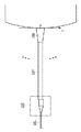
図14は、本発明の実施例3のサイクリックAWGの構成を示す平面図である。本実施例のサイクリックAWG300は、従来技術のAWGと同様に、第1の入出力導波路301、第1のスラブ導波路302、アレイ導波路303、第2のスラブ導波路304、および第2の入出力導波路305を備えている。本発明のサイクリックAWG300は、第1の入出力導波路301および第1のスラブ導波路302の間に、光スプリッタ306、2本のアーム導波路から成る遅延回路307、光モード合成カプラ308、マルチモード導波路309、直線テーパ導波路310をさらに備えている。
FIG. 14 is a plan view showing the configuration of the cyclic AWG according to the third embodiment of the present invention. The
本実施例においては、光スプリッタ306、2本のアーム導波路から成る遅延回路307、光モード合成カプラ308、マルチモード導波路309、直線テーパ導波路310が干渉回路を構成している。すなわち、複数の第1の入出力導波路の各々から入力された基底モード光の一部を、1次モード光に変換する1次モード励起機構は、光スプリッタ306、2本のアーム導波路から成る遅延回路307、光モード合成カプラ308に対応する。
In this embodiment, the
サイクリックAWG300の各部の構成パラメータは、実施例1の構成とほぼ同一であって、以下のような構成を持つ。すべての導波路については、コア・クラッド間比屈折率差が1.5%、コア厚4.5μmである。第1の入出力導波路301、アレイ導波路303、第2の入出力導波路305および遅延回路307のアーム導波路のコア幅は、4.5μmである。アレイ導波路303は50本の導波路を持ち、内側の導波路より一定量ΔLずつ順次長くなるよう設計され、ΔLは254.2475μmである。
The configuration parameters of each part of the
また第1のスラブ導波路302および第2のスラブ導波路304の長さはそれぞれ1128μmである。第1のスラブ導波路302に接続する部分の直線テーパ導波路308の配列間隔は15μmであり、第1のスラブ導波路302に接続する部分のアレイ導波路303の導波路間隔および第2のスラブ導波路304に接続する部分のアレイ導波路303の導波路間隔は、それぞれ10μmである。第1の入出力導波路301は、8本の導波路から構成されており、光合分波器としてのポート数は8である。隣接する2つのポート間の合分波光周波数間隔は100GHzで、FSRは800GHzを目標値として狙って設計されている。
The lengths of the
本実施例のサイクリックAWGによって合分波される信号光の各光周波数は実施例1と同様であり、図2で表したものである。第1の入出力導波路301のポート1からポート8において、回折次数に対応した複数の透過波長が使用され、196400GHz(波長1526.438nm)から191700GHz(波長1563.862nm)までの48チャネルの信号光が合分波される。
Each optical frequency of the signal light multiplexed / demultiplexed by the cyclic AWG of this embodiment is the same as that of the first embodiment and is shown in FIG. A plurality of transmission wavelengths corresponding to the diffraction orders are used in the
図15は、実施例3のサイクリックAWGにおける光スプリッタから直線テーパ導波路近傍をまでを拡大した図である。第1の入出力導波路301の内の1つのポート(入出力導波路)について示されており、構成要素の各符号は、図14に示したものと同一である。本実施例においてマルチモード導波路309の導波路幅は7μmであり、直線テーパ導波路310の導波路幅は、第1のスラブ導波路302に接続する部分で11.5μmである。光スプリッタ306として、方向性結合器を用いている。
FIG. 15 is an enlarged view from the optical splitter in the cyclic AWG of Example 3 to the vicinity of the linear taper waveguide. One port (input / output waveguide) in the first input /
遅延回路307は第1のアーム導波路307aおよび第2のアーム導波路307bから構成される。光モード合成カプラ308としては導波路幅が非対称な方向性結合器を用いており、第1のアーム導波路307aに接続する導波路308aの幅を2μm、第2のアーム導波路307bに接続する導波路308bの幅を7μmとした。また第1のアーム導波路307aから導波路308aへ、および、第2のアーム導波路307bから導波路308bへはテーパ導波路により滑らかに導波路幅が変換されている。導波路308a、308bの長さは、テーパ導波路を含めて500μmとした。
The
このとき導波路308aの基底モード実効屈折率と、導波路308bの1次モード実効屈折率はほぼ等しくなっており、第1のアーム導波路307aから導波路308aに入力する基底モード光は、導波路308bの1次モードに結合する。また第2のアーム導波路307bから入力する基底モード光は、そのまま導波路308bを基底モードで伝播する。したがって、マルチモード導波路309へは基底モードと1次モードが合成されて出力される。本実施例の設計では、光モード合成カプラ308の、導波路308aから導波路308bへの結合率は70%である。
本実施例のサイクリックAWGは、実施例1と同様にAWGの使用温度を回折次数に応じて微調整する温度調整タイプを前提としている。本実施例のサイクリックAWGでは、AWGごとに温度調整を行うことによって、さらに透過中心周波数のずれ量を抑えるよう動作する。したがって、本実施例のサイクリックAWGにおいて補償すべき周波数ずれ量は、実施例1における周波数ずれの特性として説明した図32に示したものとなる。各ポートにおいて補償すべき周波数ずれ量は、実施例1の場合と同じである。
At this time, the fundamental mode effective refractive index of the
The cyclic AWG of the present embodiment is premised on a temperature adjustment type in which the use temperature of the AWG is finely adjusted according to the diffraction order as in the first embodiment. The cyclic AWG of the present embodiment operates to further suppress the deviation amount of the transmission center frequency by adjusting the temperature for each AWG. Therefore, the frequency shift amount to be compensated for in the cyclic AWG of the present embodiment is the one shown in FIG. 32 described as the frequency shift characteristic in the first embodiment. The amount of frequency deviation to be compensated at each port is the same as in the first embodiment.
図16は、本発明の実施例3のサイクリックAWGの各ポートにおける透過中心波長の補償に関連するパラメータ値を示した図である。8つのポートの各ポートについて、光スプリッタ306の分岐比、第2のアーム導波路307bに対する第1のアーム導波路307aの長さの差、光モード合成カプラ308から出力する光の全パワーに対する1次モード光のパワー比率、マルチモード導波路309の長さ(μm)および直線テーパ導波路310の長さ(μm)の設計値を示した。
FIG. 16 is a diagram illustrating parameter values related to the transmission center wavelength compensation at each port of the cyclic AWG according to the third embodiment of the present invention. For each of the eight ports, the branching ratio of the
本実施例では、実施例1および実施例2における導波路オフセット106および導波路オフセット206に代えて、光スプリッタ306からマルチモード導波路309までの部分が、1次モード光の発生量および位相を制御するように動作する。本実施例では、第1の入出力導波路301の内の端に位置するポート1およびポート8において光スプリッタ306の分岐比を大きくすることによって、1次モードに変換されるパワー比を大きくしている。また、第1の入出力導波路301の内の中央付近に位置するポート4およびポート5において光スプリッタ306の分岐比をゼロとしており、1次モードへ変換されるパワーが無いように設計している。
In this embodiment, instead of the waveguide offset 106 and the waveguide offset 206 in the first embodiment and the second embodiment, the portion from the
各ポートの光スプリッタ306により第1のアーム導波路307aに分岐された一部の光パワーが、光モード合成カプラ308によって1次モードに変換される。基底モード光および1次モード光がともに、直線テーパ導波路310および第1のスラブ導波路302の接続点(直線テーパ導波路310の終端部)に到達する。この接続点へ到達する光の基底モード光および1次モード光の間の位相差は、第1のアーム導波路307aと第2のアーム導波路307bの長さの差と、所定の長さを有するマルチモード導波路309および直線テーパ導波路310により生じる。その位相差は、波長(周波数)によって変化するため、直線テーパ導波路310の終端での光フィールド分布においては、そのピーク位置が、波長によって(依存して)導波路幅方向(p軸上で)に変化する。
A part of the optical power branched to the
ここで、本実施例における、直線テーパ導波路310の終端部へ到達する光の基底モード光および1次モード光の間の位相差について考える。両モード光間の位相差は、第1のアーム導波路307aと第2のアーム導波路307bとの間の長さの差により与えられる位相差(第1の位相差)と、所定の長さを有するマルチモード導波路309および直線テーパ導波路310により与えられる位相差(第2の位相差)の和となる。本実施例では、2つの位相差の和が、補償すべき周波数ずれに応じて設定されるべき量になっていれば、2種類の位相差を分配する比率はどのようにも設定することができる。本実施例では、ポート1からポート8における第1のアーム導波路307aおよび第2のアーム導波路307bの長さをそれぞれ同一とし、すべてのポートに対して一定の位相差(第1の位相差)を与えた上で、各ポートのマルチモード導波路309の長さを調節することによって、ポートごと異なる位相差(第2の位相差)を調整している。
Here, the phase difference between the fundamental mode light and the first-order mode light of the light reaching the end of the
したがって、本実施例では、1次モード励起機構は、光スプリッタと、前記光スプリッタに接続する第1のアーム導波路および第2のアーム導波路と、前記第1のアーム導波路および第2のアーム導波路に接続し、前記第2のアーム導波路から入力する基底モード光を1次モードに変換し、前記第1のアーム導波路から入力する基底モードと合流させて出力する光モード合成カプラで構成される。基底モード光および1次モード光の間の位相差は、第1のアーム導波路と第2のアーム導波路の設定された光路長差および所定の長さを有するマルチモード導波路309とテーパ導波路310によって、波長に依存して変化することになる。
Therefore, in this embodiment, the first-order mode excitation mechanism includes an optical splitter, a first arm waveguide and a second arm waveguide connected to the optical splitter, and the first arm waveguide and the second arm waveguide. An optical mode combining coupler connected to the arm waveguide, converting the fundamental mode light input from the second arm waveguide to a primary mode, and combining the fundamental mode input from the first arm waveguide and outputting Consists of. The phase difference between the fundamental mode light and the first-order mode light is different from that of the
本実施例においても、1次モード光の発生量および位相を調整し、スラブ導波路の接続部における導波路幅方向の光フィールドのピーク位置を調整することができる。サイクリックAWGにおける直線テーパ導波路終端の光フィールドのピーク位置の変化によって、従来のサイクリックAWGが持っていた透過中心周波数のずれが補正されることになる点で、実施例1および実施例2と全く同様に動作する。 Also in this embodiment, the generation amount and phase of the primary mode light can be adjusted, and the peak position of the optical field in the waveguide width direction at the connection portion of the slab waveguide can be adjusted. In the first and second embodiments, the transmission center frequency shift of the conventional cyclic AWG is corrected by the change in the peak position of the optical field at the end of the linear taper waveguide in the cyclic AWG. Works exactly the same.
図17は、本実施例における、直線テーパ導波路終端の光フィールド分布ピーク位置の、伝搬する光波の周波数による変化をポートごとに示した図である。ここで縦軸のピーク位置p(μm)は、図15におけるp座標軸の位置に対応し、p=0は直線テーパ導波路の中心位置となる。横軸は光波の周波数であって、波長番号1〜48の範囲の周波数に対応する。既に述べたように、縦軸の光フィールド分布のピーク位置のシフトによって透過中心周波数を変更し補正することができる。したがって、図17の縦軸は、周波数ずれの「補正量」を意味する。当然のことではあるが、実施例1と同じ周波数ずれを補正するための補正量の特性であるため、図6および図17はほとんど同一の特性となる。
FIG. 17 is a diagram illustrating the change of the peak position of the optical field distribution at the end of the linear taper waveguide according to the present embodiment depending on the frequency of the propagating light wave for each port. Here, the peak position p (μm) on the vertical axis corresponds to the position of the p coordinate axis in FIG. 15, and p = 0 is the center position of the linear taper waveguide. The horizontal axis represents the frequency of the light wave and corresponds to the frequency in the range of
本実施例では、透過中心周波数のずれの補正は、ポートごとに、光スプリッタ306の分岐比を設定して、1次モード光の発生量を制御して行われる。またその補正量は、周波数によって変化し、1つのポート内に現れる異なる複数の周波数の光波に対して、周波数ずれ量の周波数特性に適合するように、複数の透過中心波長を同時に一括して補正することができる。すなわち、1つのポート内に現れる異なる複数の周波数の光波に対して、周波数ずれ補正量は、周波数によって変化している。
In this embodiment, the correction of the transmission center frequency deviation is performed by setting the branching ratio of the
図18は、実施例2のサイクリックAWGについて、透過中心波長のITU−Tクリッドからのずれ量を示す図である。本実施例のサイクリックAWGは温度調整タイプであり、使用する回折次数によって一定に保つ温度を微調整している。本実施例のサイクリックAWGにおけるITU−Tクリッドからからの周波数ずれは、最大でも±1.2GHz(±0.010nm)であり、従来のサイクリックAWG(図32)と比較して、周波数ずれ量が約1/5に低減されている。透過中心周波数(波長)がよりITU−Tクリッドに整合したサイクリックAWGが実現されている。 FIG. 18 is a diagram illustrating a deviation amount of the transmission center wavelength from the ITU-T crid in the cyclic AWG according to the second embodiment. The cyclic AWG of this embodiment is a temperature adjustment type, and finely adjusts the temperature to be kept constant according to the diffraction order used. In the cyclic AWG of the present embodiment, the maximum frequency deviation from the ITU-T crid is ± 1.2 GHz (± 0.010 nm), which is a frequency deviation compared to the conventional cyclic AWG (FIG. 32). The amount is reduced to about 1/5. A cyclic AWG in which the transmission center frequency (wavelength) is more matched to the ITU-T grid is realized.
本実施例においては、図15に示したように、光モード合成カプラ308として、非対称な方向性結合器を適用したが、光モード合成カプラ308の具体的な構成は方向性結合器だけに限定されない。
In this embodiment, as shown in FIG. 15, an asymmetric directional coupler is applied as the optical
図19は、光モード合成カプラの別の構成例を拡大して示した図である。図19の構成の光モード合成カプラ308は、図15に示したのと同様に非対称な方向性結合器ではあるが、導波路308aに接続する出力導波路は、溝311によって終端されている。ここで、溝311には光波を吸収するような遮光材料が挿入されている。また遮光材料と出力導波路との界面は導波路に垂直ではなく、垂直面から8度傾いている。図19の光モード合成カプラの構成を採用することにより、図15の構成に比較して、導波路308aから導波路308bに結合せずに僅かに残る光を遮断して、第1のスラブ導波路302などに迷光が侵入することを抑制する。また、迷光の反射も抑制することができるため、クロストークおよび反射特性により優れたサイクリックAWGを実現可能である。
FIG. 19 is an enlarged view showing another configuration example of the optical mode synthesis coupler. The optical
図20は、光モード合成カプラのさらに別の構成例を拡大して示した図である。図20の構成の光モード合成カプラ308は、図15に示したのと同様に非対称な方向性結合器ではあるが、導波路308aはその幅が徐々に狭くなり、幅が無くなって終端する構造になっている。このとき、導波路308a、308bの長さは1500μmに設計されている。図20の光モード合成カプラの構成を採用することにより、図15の構成に比較して、導波路308aから導波路308bへの光波の結合率をほぼ100%にすることができる。このため、損失特性により優れたサイクリックAWGが実現可能である。
FIG. 20 is an enlarged view showing still another configuration example of the optical mode synthesis coupler. The optical
また本実施例においては、図15のように、光スプリッタ306として、単一の方向性結合器を適用したが、光スプリッタ306はこの構成に限定されない。例えば、非対称Y分岐回路、MMI、波長無依存カプラ(WINC)によっても実現することができる。
In the present embodiment, as shown in FIG. 15, a single directional coupler is applied as the
本実施例においても、実施例1と同様に、サイクリックAWGにおける直線テーパ導波路終端の光フィールドのピーク位置の変化によって、従来のサイクリックAWGが持っていた透過中心周波数のずれが補正されることになる。この補正は、ポートごとに、光スプリッタ306の分岐比を設定して、1次モード光の発生量を制御して行われる。またその補正量は、周波数によって変化し、1つのポート内に現れる異なる複数の周波数の光波に対して、周波数ずれ量の周波数特性に適合するように、複数の透過中心波長を同時に一括して補正することができる。実施例3の構成を、アサーマル化することもできる。次の実施例は、実施例3のサイクリックAWGの構成に対して、実施例2のアサーマル化AWGの構成を組み合わせたものとなる。
Also in the present embodiment, similarly to the first embodiment, the shift of the transmission center frequency that the conventional cyclic AWG has is corrected by the change in the peak position of the optical field at the end of the linear taper waveguide in the cyclic AWG. It will be. This correction is performed by setting the branching ratio of the
図21は、本発明の実施例4のサイクリックAWGの構成を示す平面図である。本実施例のサイクリックAWG400は、従来技術のAWGと同様に、第1の入出力導波路401、第1のスラブ導波路402、アレイ導波路403、第2のスラブ導波路404、および第2の入出力導波路405を備えている。本発明のサイクリックAWG400は、実施例3と同様に、第1の入出力導波路401および第1のスラブ導波路402の間に、光スプリッタ406、2本のアーム導波路から成る遅延回路407、光モード合成カプラ408、マルチモード導波路409、直線テーパ導波路410を備えている。本実施例では、さらに、温度調整を不要とするために、第1のスラブ導波路402の途中に、導波路を分断する溝409が形成され、溝409内にはシリコーン樹脂が充填されている。この溝409によって、アサーマルサイクリックAWGを実現する。
FIG. 21 is a plan view showing the configuration of the cyclic AWG according to the fourth embodiment of the present invention. The
アサーマルサイクリックAWG400の各部の構成パラメータは、以下のような構成を持つ。すべての導波路については、コア・クラッド間比屈折率差が1.5%、コア厚4.5μmである。第1の入出力導波路401、アレイ導波路403、第2の入出力導波路405、および遅延回路407のアーム導波路のコア幅は4.5μmである。アレイ導波路403は50本の導波路を持ち、内側の導波路より一定量ΔLずつ順次長くなるよう設計され、ΔLは254.60μmである。
The configuration parameters of each part of the athermal
図21に示したように、溝409は複数の溝に分割されている。これは、複数の溝を構成する場合のほうが、単一の溝で構成する場合と比べて、放射損失をより低減することができるからである。アレイ導波路403では、各々の導波路が一定量ΔL順次長くなるよう設計されている。すなわち、隣り合う2つの導波路の導波路長の差がΔLとなっている。第1のスラブ導波路402において複数の溝409によって分断される長さの和は、アレイ導波路403の各導波路長に応じて、各導波路に入力する光波が、ΔLに比例した量のΔL´=1/34×ΔL順次長くなるような形状をしている。
As shown in FIG. 21, the
また、第1のスラブ導波路402および第2のスラブ導波路404の長さはそれぞれ1128μmである。第1のスラブ導波路402に接続する部分の直線テーパ導波路408の配列間隔は15μmであり、第1のスラブ導波路402に接続する部分のアレイ導波路403の導波路間隔および第2のスラブ導波路404に接続する部分のアレイ導波路403の導波路間隔は、それぞれ10μmである。第1の入出力導波路401は、8本の導波路から構成されており、光合分波器としてのポート数は8である。隣接する2つのポート間の合分波光周波数間隔は100GHzで、FSRは800GHzを目標値として狙って設計されている。
The lengths of the
本実施例のサイクリックAWGによって合分波される信号光の各光周波数は実施例1〜実施例3と同様であり、図2で表したものである。第1の入出力導波路401のポート1からポート8において、回折次数に対応した複数の透過波長が使用され、196400GHz(波長1526.438nm)から191700GHz(波長1563.862nm)までの48チャネルの信号光が合分波される。
Each optical frequency of the signal light multiplexed / demultiplexed by the cyclic AWG of the present embodiment is the same as that of the first to third embodiments and is shown in FIG. A plurality of transmission wavelengths corresponding to the diffraction orders are used in
図22は、実施例4のサイクリックAWGにおける光スプリッタから直線テーパ導波路近傍をまでを拡大した図である。第1の入出力導波路401の内の1つのポート(入出力導波路)について示されており、構成要素の各符号は、図21に示したものと同一である。本実施例においてマルチモード導波路409の導波路幅は7μmであり、直線テーパ導波路410の導波路幅は、第1のスラブ導波路402に接続する部分で11.5μmである。光スプリッタ406として、方向性結合器を用いている。
FIG. 22 is an enlarged view from the optical splitter to the vicinity of the linear taper waveguide in the cyclic AWG of the fourth embodiment. This is shown for one port (input / output waveguide) in the first input /
遅延回路407は第1のアーム導波路407aおよび第2のアーム導波路407bから構成される。光モード合成カプラ408としては導波路幅が非対称な方向性結合器を用いており、第1のアーム導波路407aに接続する導波路408aの幅を2μm、第2のアーム導波路407bに接続する導波路408bの幅を7μmとした。また第1のアーム導波路407aから導波路408aへ、および、第2のアーム導波路407bから導波路408bへはテーパ導波路により滑らかに導波路幅が変換されている。導波路408a、408bの長さは、テーパ導波路を含めて500μmとした。
The
このとき導波路408aの基底モード実効屈折率と、導波路408bの1次モード実効屈折率はほぼ等しくなっており、第1のアーム導波路407aから導波路408aに入力する基底モード光は、導波路408bの1次モードに結合する。また第2のアーム導波路407bから入力する基底モード光は、そのまま導波路408bを基底モードで伝播する。したがって、マルチモード導波路409へは基底モードと1次モードが合成されて出力される。本実施例の設計では、光モード合成カプラ408の、導波路408aから導波路408bへの結合率は70%である。
At this time, the fundamental mode effective refractive index of the
図23は、本発明の実施例4のサイクリックAWGの各ポートにおける透過中心波長の補償に関連するパラメータ値を示した図である。8つのポートの各ポートについて、光スプリッタ406の分岐比、第2のアーム導波路407bに対する第1のアーム導波路407aの長さの差、光モード合成カプラ408から出力する光の全パワーに対する1次モード光のパワー比率、マルチモード導波路409の長さ(μm)および直線テーパ導波路410の長さ(μm)の設計値を示した。
FIG. 23 is a diagram illustrating parameter values related to the transmission center wavelength compensation at each port of the cyclic AWG according to the fourth embodiment of the present invention. For each of the eight ports, the branching ratio of the
本実施例も、実施例3と同様に、光スプリッタ406からマルチモード導波路409までの部分が、1次モード光の発生量および位相を制御するように動作する。実施例3と異なり、本実施例のサイクリックAWGは、アサーマル化されているのでAWGの使用温度の微調整は行わない非温度調整タイプを前提としている。したがって、本実施例のサイクリックAWGが補償すべき周波数ずれは、実施例2と同じく図31に示したものとなる。すなわち、実施例2と同様に、図34が、アサーマル化されたサイクリックAWGのポート毎の周波数ずれ量を示している。
In the present embodiment, as in the third embodiment, the portion from the
したがって、図34に示したポート毎に異なる周波数ずれの最大量および周波数特性(傾き・形状)に応じた補償をすることで、実施例3の場合と同様に、各々のポートに対して、ポートごとの周波数ずれ量の周波数特性に適合するように、効果的に周波数ずれを抑えることができる。また、1つのポート内に現われる複数の異なる周波数に対する補正量の周波数特性も、図34の各プロット点から把握できるP1〜P8の各曲線に基づいて、簡単に決定できる。 Therefore, by performing compensation according to the maximum amount of frequency deviation and frequency characteristics (inclination / shape) different for each port shown in FIG. The frequency shift can be effectively suppressed so as to match the frequency characteristics of the frequency shift amount for each. Further, the frequency characteristics of the correction amounts for a plurality of different frequencies appearing in one port can be easily determined based on the respective curves P1 to P8 that can be grasped from the respective plot points in FIG.
本実施例では、各ポートの光スプリッタ406により第1のアーム導波路407aに分岐された一部の光パワーが、光モード合成カプラ408によって1次モードに変換される。基底モード光および1次モード光がともに、直線テーパ導波路410および第1のスラブ導波路402の接続点(直線テーパ導波路410の終端部)に到達する。この接続点へ到達する光の基底モード光および1次モード光の間の位相差は、第1のアーム導波路407aおよび第2のアーム導波路407bの間の長さの差と、所定の長さを有するマルチモード導波路409および直線テーパ導波路410により生じる。その位相差は、波長(周波数)によって変化するため、直線テーパ導波路410の終端での光フィールド分布においては、そのピーク位置は、波長によって(依存して)導波路幅方向(p軸上で)に変化する。
In this embodiment, a part of the optical power branched to the
実施例3と同様に、本実施例においても、第1のアーム導波路407aと第2のアーム導波路407bとの間の長さの差により与えられる位相差(第1の位相差)と、所定の長さを有するマルチモード導波路409および直線テーパ導波路410により与えられる位相差(第2の位相差)の和となる。本実施例では、ポート1からポート8における第1のアーム導波路407aおよび第2のアーム導波路407bの長さをそれぞれ同一とし、すべてのポートに対して一定の位相差(第1の位相差)を与えた上で、各ポートのマルチモード導波路409の長さを調節することによって、ポートごと異なる位相差(第2の位相差)を調整している。
Similar to the third embodiment, also in this embodiment, the phase difference (first phase difference) given by the difference in length between the
したがって、本実施例においても、1次モード光の発生量および位相を調整し、スラブ導波路の接続部における導波路幅方向の光フィールドのピーク位置を調整する。サイクリックAWGにおける直線テーパ導波路終端の光フィールドのピーク位置の変化によって、従来のサイクリックAWGが持っていた透過中心周波数のずれは補正されることになる点で、実施例1〜実施例3と全く同様に動作する。 Therefore, also in the present embodiment, the generation amount and phase of the primary mode light are adjusted, and the peak position of the optical field in the waveguide width direction at the connection portion of the slab waveguide is adjusted. The shift of the transmission center frequency of the conventional cyclic AWG is corrected by the change in the peak position of the optical field at the end of the linear taper waveguide in the cyclic AWG. Works exactly the same.
再び図23を参照すると、本実施例では、ポート1からポート8にかけてポート番号が大きいほど、光スプリッタ406の分岐比を順次大きくし、1次モードに変換されるパワー比を相対的に大きくしている(2.5%から6.0%へ)。このように、補償すべき周波数ずれ量の最大値に応じて、1次モード光の発生量を光スプリッタ406の分岐比で制御している。
Referring to FIG. 23 again, in this embodiment, as the port number increases from
図24は、本実施例における、直線テーパ導波路終端の光フィールド分布ピーク位置の、伝搬する光波の周波数による変化をポートごとに示した図である。ここで縦軸のピーク位置p(μm)は、図22におけるp座標軸の位置に対応し、p=0は直線テーパ導波路の中心位置となる。横軸は光波の周波数であって、波長番号1〜48の範囲の周波数に対応する。既に述べたように、縦軸の光フィールド分布のピーク位置のシフトによって透過中心周波数を変更し補正することができる。したがって、図24の縦軸は、周波数ずれの「補正量」を意味する。当然のことではあるが、実施例2と同じ周波数ずれを補正するための補正量の特性であるため、図12および図24はほとんど同一の特性となる。
FIG. 24 is a diagram illustrating the change of the peak position of the optical field distribution at the end of the linear taper waveguide according to the frequency of the propagating light wave for each port in this example. Here, the peak position p (μm) on the vertical axis corresponds to the position of the p coordinate axis in FIG. 22, and p = 0 is the center position of the linear taper waveguide. The horizontal axis represents the frequency of the light wave and corresponds to the frequency in the range of
本実施例では、透過中心周波数のずれの補正は、ポートごとに、光スプリッタ406の分岐比を設定して、1次モード光の発生量を制御して行われる。またその補正量は、周波数によって変化し、1つのポート内に現れる異なる複数の周波数の光波に対して、周波数ずれ量の周波数特性に適合するように、複数の透過中心波長を同時に一括して補正することができる。すなわち、1つのポート内に現れる異なる複数の周波数の光波に対して、周波数ずれ補正量は周波数によって変化している。
In the present embodiment, the correction of the transmission center frequency deviation is performed by setting the branching ratio of the
図25は、実施例4のサイクリックAWGについて、透過中心波長のITU−Tクリッドからのずれ量を示す図である。本実施例のサイクリックAWGはアサーマル化されており、非温度調整タイプであって、AWGの温度調節は行われない。本実施例のサイクリックAWGにおけるITU−Tクリッドからからの周波数ずれは、最大でも±1.7GHz(±0.014nm)であり、従来のサイクリックAWGでアサーマル化を前提とした場合(図31)に比較して、周波数ずれ量が約1/5に低減されている。透過中心周波数(波長)がよりITU−Tクリッドに整合したサイクリックAWGが実現されている。 FIG. 25 is a diagram illustrating a deviation amount of the transmission center wavelength from the ITU-T cluded for the cyclic AWG of the fourth embodiment. The cyclic AWG of the present embodiment is athermalized, is a non-temperature adjustment type, and the temperature of the AWG is not adjusted. In the cyclic AWG of this embodiment, the frequency deviation from the ITU-T clad is ± 1.7 GHz (± 0.014 nm) at the maximum, and when the conventional cyclic AWG is assumed to be athermal (FIG. 31). ), The frequency shift amount is reduced to about 1/5. A cyclic AWG in which the transmission center frequency (wavelength) is more matched to the ITU-T grid is realized.
本実施例においては、図22に示したように、光モード合成カプラ408として、非対称な方向性結合器を適用したが、光モード合成カプラ408の具体的な構成は方向性結合器だけに限定されない。実施例3で説明した図19のように、導波路408aに接続する出力導波路を遮光材料が挿入された溝で終端し、迷光や反射を抑制する構成を採用することができる。また、図20のように導波路408aの幅を徐々に狭めて終端し、導波路408bへの光の結合率をほぼ100%にする構成も適用可能である。
In this embodiment, as shown in FIG. 22, an asymmetric directional coupler is applied as the optical
また本実施例においては、図22のように、光スプリッタ406として、単一の方向性結合器を適用したが、光スプリッタ406の具体的な構成は方向性結合器だけに限定されない。例えば非対称Y分岐回路、MMI、波長無依存カプラ(WINC)によっても実現される。
In this embodiment, as shown in FIG. 22, a single directional coupler is applied as the
本実施例では、温度調整を不要とするための溝411を第1のスラブ導波路402中に設けている。しかしながらこの構成に限られず、例えば、第2のスラブ導波路404やアレイ導波路403の中に複数の溝411を設け、シリコーン樹脂を充填するようにしても良いことは言うまでもない。
In this embodiment, a
既に述べたとおり、実施例3および実施例4においては、直線テーパ導波路の終端部へ到達する光の基底モード光および1次モード光の間の位相差について、第1のアーム導波路と第2のアーム導波路との間の長さの差により与えられる位相差(第1の位相差)と、所定の長さを有するマルチモード導波路および直線テーパ導波路により与えられる位相差(第2の位相差)の和となる。したがって、2つの位相差の和が、補償すべき周波数ずれに応じて設定されるべき量として、2種類の位相差を適切に分配することができる。したがって、図16および図23に示したのとは異なり、第1のアーム導波路と第2のアーム導波路との間の長さをポート毎に可変することもできる。 As described above, in the third and fourth embodiments, the first arm waveguide and the first mode waveguide are compared with each other in terms of the phase difference between the fundamental mode light and the first-order mode light that reach the end of the linear taper waveguide. The phase difference (first phase difference) given by the length difference between the two arm waveguides and the phase difference (second phase) given by the multimode waveguide and the linear taper waveguide having a predetermined length. Phase difference). Therefore, the two types of phase differences can be appropriately distributed as the amount that the sum of the two phase differences should be set according to the frequency shift to be compensated. Therefore, unlike those shown in FIGS. 16 and 23, the length between the first arm waveguide and the second arm waveguide can be varied for each port.
ここで、図17および図24に示した直線テーパ導波路終端の光フィールド分布ピーク位置の、伝搬する光波の周波数による変化との関連から、上述の2種類の位相差は次のように説明できる。既に述べたように、図17および図24は、周波数ずれの「補正カーブ」に対応する。この補正カーブは、サイン関数状の形状を持っている。 Here, the above two types of phase differences can be explained as follows in relation to the change in the optical field distribution peak position at the end of the linear taper waveguide shown in FIGS. 17 and 24 depending on the frequency of the propagating light wave. . As already described, FIGS. 17 and 24 correspond to “correction curves” of frequency shift. The correction curve has a sine function shape.
具体的には、基底モード光および1次モード光の位相差は、サイン関数状のカーブの次のパラメータを利用して調整を行っていると見ることができる。 Specifically, it can be considered that the phase difference between the fundamental mode light and the first-order mode light is adjusted using the next parameter of the sine function-like curve.
サイン関数状の補正カーブyは、xを正規化した周波数とすると、単純化すれば、例えば次の式のように表現できる。
y=A×sin(B×x+C) 式(2)
The correction curve y in the form of a sine function can be expressed, for example, by the following equation if it is simplified if x is a normalized frequency.
y = A * sin (B * x + C) Formula (2)
ここで、調整できるパラメータの1つは、サイン関数のCであって、Cを設定することによって、補正カーブのピーク波長(周波数)を設定できる。また、Bを設定することによって、補正カーブの周期すなわち波長依存性を設定できる。実施例3および実施例4では、第1のアーム導波路と第2のアーム導波路との間の長さの差による第1の位相差よって上記サイン関数状カーブの周期(B)を調整し、マルチモード導波路の長さによる第2の位相差によってサインカーブのピーク波長(C)を調整していると見ることができる。これは2種類の位相差を分配する一例であり、本発明においては、2つの位相差の和が、補償すべき周波数ずれに応じて設定されるべき量として、2種類の位相差を適切に分配することができる 。尚、実施例1、実施例2ではBおよびC両方の調整をマルチモード導波路の長さだけで行っていることになる。 Here, one of the parameters that can be adjusted is C of the sine function, and by setting C, the peak wavelength (frequency) of the correction curve can be set. Further, by setting B, the period of the correction curve, that is, the wavelength dependency can be set. In Example 3 and Example 4, the period (B) of the sine function curve is adjusted by the first phase difference due to the difference in length between the first arm waveguide and the second arm waveguide. It can be seen that the peak wavelength (C) of the sine curve is adjusted by the second phase difference depending on the length of the multimode waveguide. This is an example of distributing two types of phase differences, and in the present invention, the sum of the two phase differences is appropriately set as an amount to be set according to the frequency shift to be compensated. Can be distributed. In the first and second embodiments, both B and C are adjusted only by the length of the multimode waveguide.
以上の4つの実施例から分かるように、本発明の温度調整タイプのサイクリックAWG光波長合分波回路またはアサーマルタイプのサイクリックAWG光波長合分波回路では、従来技術において課題であった、ITU−Tグリッドからの透過中心波長のずれが抑制され、透過中心波長の精度に優れた、光波長合分波回路を得ることができる。 As can be seen from the above four embodiments, the temperature control type cyclic AWG optical wavelength multiplexing / demultiplexing circuit or the athermal type cyclic AWG optical wavelength multiplexing / demultiplexing circuit of the present invention was a problem in the prior art. A shift of the transmission center wavelength from the ITU-T grid is suppressed, and an optical wavelength multiplexing / demultiplexing circuit having excellent transmission center wavelength accuracy can be obtained.
全ての実施例では、導波路の比屈折率差、コア幅及びコア厚を特定の値に限定したが、本発明の適用範囲は、この値に限定されるものではない。 In all the examples, the relative refractive index difference, the core width, and the core thickness of the waveguide are limited to specific values, but the scope of application of the present invention is not limited to these values.
全ての実施の形態では、AWGの設計パラメータを特定の値を例として説明したが、本発明の適用範囲は、必要とされる合分波特性やシステムのチャンル構成に応じて、また、導波路の構成に応じて、様々に変形して実現できるものであって、実施例のパラメータに限定されるものではない。 In all the embodiments, the AWG design parameters have been described by taking specific values as examples. However, the scope of the present invention can be determined according to the required multiplexing / demultiplexing characteristics and the system channel configuration. Depending on the configuration of the waveguide, it can be variously modified and is not limited to the parameters of the embodiment.
全ての実施の形態では、合分波される信号の波長数、波長(周波数)間隔を特定の例について説明したが、本発明は、他の構成に対しても様々に変形して適用可能であって、実施例のパラメータに限定されるものではない。 In all the embodiments, specific examples of the number of wavelengths and wavelength (frequency) intervals of signals to be multiplexed / demultiplexed have been described. However, the present invention can be applied to other configurations with various modifications. Thus, it is not limited to the parameters of the embodiment.
実施例2および実施例4では、温度補償材料としてシリコーン樹脂を使用したが、本発明は、この材料に限定されるものではなく、導波路の実効屈折率温度係数と異なる屈折率温度係数を有する他のどのような材料も適用することができる。 In Example 2 and Example 4, silicone resin was used as the temperature compensation material, but the present invention is not limited to this material and has a refractive index temperature coefficient different from the effective refractive index temperature coefficient of the waveguide. Any other material can be applied.
全ての実施例においては、第2の入出力導波路および第2のスラブ導波路を直接接続する構成を例として説明してきたが、この接続部に直線テーパ導波路を適用しもて良い。この場合は、サイクリックAWGの透過率形状はガウシアンとなる。さらには、第2の入出力導波路およびスラブ導波路の接続部に2次モードを励起するようなテーパ導波路、例えばパラボラ形状のテーパ導波路を適用しても良い。この場合は、サイクリックAWGは平坦な透過率形状を実現することが可能である。 In all the embodiments, the configuration in which the second input / output waveguide and the second slab waveguide are directly connected has been described as an example. However, a linear taper waveguide may be applied to this connection portion. In this case, the transmittance shape of the cyclic AWG is Gaussian. Furthermore, a tapered waveguide that excites the secondary mode, for example, a parabolic tapered waveguide may be applied to the connection portion of the second input / output waveguide and the slab waveguide. In this case, the cyclic AWG can realize a flat transmittance shape.
本発明は、一般的に通信システムに利用することができる。特に、光通信システムに利用することができる。 The present invention is generally applicable to communication systems. In particular, it can be used in an optical communication system.
100、200、300、400、9100 サイクリックAWG
101、201、301、401、9101 1の入出力導波路
102、202、302、402、9102 第1のスラブ導波路
103、203、303、403、9103 アレイ導波路
104、204、304、404、9104 第2のスラブ導波路
105、205、305、405、9105 第2の入出力導波路
106、206 導波路オフセット
107、207、309、409 マルチモード導波路
108、208、310、410 直線テーパ導波路
210 シリコン基板
211 導波路コア
212 クラッド
306、406 光スプリッタ
307、407 遅延回路
307a、307b、407a、407b アーム導波路
308、408 光モード合成カプラ
308a、408a、308b、408b 導波路
209、311、411 溝
9200 サイクリックAWGの回路
9201 第1の入出力導波路に接続するポート
9202 第2の入出力導波路にポート
9400 6分岐のカプラまたは6ポートの波長群合分波フィルタ
9401、9402、9403、9404、9405、9406 サイクリックAWG
100, 200, 300, 400, 9100 Cyclic AWG
101, 201, 301, 401, 9101 11 input /
Claims (7)
各々が干渉回路を介して前記第1のスラブ導波路に光学的に接続された複数の第1の入出力導波路と、前記第2のスラブ導波路に接続された第2の入出力導波路とをさらに備えており、
前記干渉回路は、
前記複数の第1の入出力導波路の各々から入力された基底モード光の一部を、1次モード光に変換する1次モード励起機構と、
前記1次モード励起機構に光学的に接続し、少なくとも基底モード光および1次モード光が伝搬可能であって、前記基底モード光および前記1次モード光の間に所定の透過波長に対して所定の位相差を与えるマルチモード導波路とを有し、
前記干渉回路と前記第1のスラブ導波路との接続面において形成された光フィールド分布のピーク位置が、波長によって前記マルチモード導波路の導波路幅方向に変化し、前記変化によって、前記複数の回折次数に対応した透過波長の、規格化されたグリッドからのずれを補償するよう構成されたこと
を特徴とする光波長合分波回路。 An arrayed waveguide consisting of waveguides that become longer sequentially with a predetermined optical path length difference, a first slab waveguide connected to one end of the arrayed waveguide, and a second slab guide connected to the other end of the arrayed waveguide In a wavelength multiplexing / demultiplexing circuit including a waveguide and using a transmission wavelength corresponding to a plurality of diffraction orders,
A plurality of first input / output waveguides each optically connected to the first slab waveguide via an interference circuit, and a second input / output waveguide connected to the second slab waveguide And
The interference circuit is
A primary mode excitation mechanism for converting a part of the fundamental mode light input from each of the plurality of first input / output waveguides into primary mode light;
Optically connected to the first-order mode excitation mechanism so that at least the fundamental mode light and the first-order mode light can propagate, and a predetermined transmission wavelength is determined between the fundamental-mode light and the first-order mode light. A multimode waveguide that gives a phase difference of
The peak position of the optical field distribution formed at the connection surface between the interference circuit and the first slab waveguide changes in the waveguide width direction of the multimode waveguide according to the wavelength, and the change causes the plurality of An optical wavelength multiplexing / demultiplexing circuit configured to compensate a deviation of a transmission wavelength corresponding to a diffraction order from a standardized grid.
前記基底モード光および前記1次モード光の間の位相差は、前記第1のアーム導波路と第2のアーム導波路の設定された光路長差において、波長によって変化することを特徴とする請求項1乃至3いずれかに記載の光波長合分波回路。 The primary mode excitation mechanism is connected to an optical splitter, a first arm waveguide and a second arm waveguide connected to the optical splitter, and the first arm waveguide and the second arm waveguide. , Comprising an optical mode synthesis coupler that converts the fundamental mode light input from the second arm waveguide into a primary mode, and combines and outputs the fundamental mode input from the first arm waveguide;
The phase difference between the fundamental mode light and the first-order mode light varies depending on a wavelength in a set optical path length difference between the first arm waveguide and the second arm waveguide. Item 4. The optical wavelength multiplexing / demultiplexing circuit according to any one of Items 1 to 3.
Priority Applications (1)
| Application Number | Priority Date | Filing Date | Title |
|---|---|---|---|
| JP2013254211A JP6126522B2 (en) | 2013-12-09 | 2013-12-09 | Optical wavelength multiplexing / demultiplexing circuit |
Applications Claiming Priority (1)
| Application Number | Priority Date | Filing Date | Title |
|---|---|---|---|
| JP2013254211A JP6126522B2 (en) | 2013-12-09 | 2013-12-09 | Optical wavelength multiplexing / demultiplexing circuit |
Publications (2)
| Publication Number | Publication Date |
|---|---|
| JP2015114378A true JP2015114378A (en) | 2015-06-22 |
| JP6126522B2 JP6126522B2 (en) | 2017-05-10 |
Family
ID=53528250
Family Applications (1)
| Application Number | Title | Priority Date | Filing Date |
|---|---|---|---|
| JP2013254211A Expired - Fee Related JP6126522B2 (en) | 2013-12-09 | 2013-12-09 | Optical wavelength multiplexing / demultiplexing circuit |
Country Status (1)
| Country | Link |
|---|---|
| JP (1) | JP6126522B2 (en) |
Cited By (4)
| Publication number | Priority date | Publication date | Assignee | Title |
|---|---|---|---|---|
| JP2020071238A (en) * | 2018-10-29 | 2020-05-07 | 日本電信電話株式会社 | Wavelength checker |
| CN114114532A (en) * | 2021-11-05 | 2022-03-01 | 武汉永鼎光电子技术有限公司 | Method for implementing spectrum shape transformation of arrayed waveguide grating |
| EP4220255A1 (en) * | 2022-01-27 | 2023-08-02 | The Boeing Company | Waveguide system |
| CN119575548A (en) * | 2024-07-08 | 2025-03-07 | 电子科技大学 | A coupling optimization method for low-loss wavelength division multiplexer |
Citations (8)
| Publication number | Priority date | Publication date | Assignee | Title |
|---|---|---|---|---|
| JP2002323626A (en) * | 2001-02-20 | 2002-11-08 | Furukawa Electric Co Ltd:The | Optical wavelength multiplexer / demultiplexer and optical multiplexer / demultiplexer system |
| JP2003513330A (en) * | 1999-11-01 | 2003-04-08 | アルカテル・オプトロニクス・ユー・ケイ・リミテツド | Passband smoothing phased array |
| JP2003149474A (en) * | 2001-11-16 | 2003-05-21 | Nippon Telegr & Teleph Corp <Ntt> | Array waveguide type wavelength multiplexer / demultiplexer |
| US6608948B2 (en) * | 2000-12-18 | 2003-08-19 | Jds Fitel Inc. | Periodic arrayed waveguide grating multiplexer/demultiplexer |
| US20070274632A1 (en) * | 2006-04-28 | 2007-11-29 | Gemfire Corporation | Arrayed waveguide grating with reduced channel passband asymmetry |
| JP2010026302A (en) * | 2008-07-22 | 2010-02-04 | Nippon Telegr & Teleph Corp <Ntt> | Optical wavelength division multiplexing circuit |
| JP2010044350A (en) * | 2008-07-14 | 2010-02-25 | Nippon Telegr & Teleph Corp <Ntt> | Optical wavelength multiplexing and demultiplexing circuit |
| US20100247036A1 (en) * | 2009-03-31 | 2010-09-30 | Infinera Corporation | Flat-top response arrayed waveguide grating |
-
2013
- 2013-12-09 JP JP2013254211A patent/JP6126522B2/en not_active Expired - Fee Related
Patent Citations (8)
| Publication number | Priority date | Publication date | Assignee | Title |
|---|---|---|---|---|
| JP2003513330A (en) * | 1999-11-01 | 2003-04-08 | アルカテル・オプトロニクス・ユー・ケイ・リミテツド | Passband smoothing phased array |
| US6608948B2 (en) * | 2000-12-18 | 2003-08-19 | Jds Fitel Inc. | Periodic arrayed waveguide grating multiplexer/demultiplexer |
| JP2002323626A (en) * | 2001-02-20 | 2002-11-08 | Furukawa Electric Co Ltd:The | Optical wavelength multiplexer / demultiplexer and optical multiplexer / demultiplexer system |
| JP2003149474A (en) * | 2001-11-16 | 2003-05-21 | Nippon Telegr & Teleph Corp <Ntt> | Array waveguide type wavelength multiplexer / demultiplexer |
| US20070274632A1 (en) * | 2006-04-28 | 2007-11-29 | Gemfire Corporation | Arrayed waveguide grating with reduced channel passband asymmetry |
| JP2010044350A (en) * | 2008-07-14 | 2010-02-25 | Nippon Telegr & Teleph Corp <Ntt> | Optical wavelength multiplexing and demultiplexing circuit |
| JP2010026302A (en) * | 2008-07-22 | 2010-02-04 | Nippon Telegr & Teleph Corp <Ntt> | Optical wavelength division multiplexing circuit |
| US20100247036A1 (en) * | 2009-03-31 | 2010-09-30 | Infinera Corporation | Flat-top response arrayed waveguide grating |
Cited By (6)
| Publication number | Priority date | Publication date | Assignee | Title |
|---|---|---|---|---|
| JP2020071238A (en) * | 2018-10-29 | 2020-05-07 | 日本電信電話株式会社 | Wavelength checker |
| JP7124638B2 (en) | 2018-10-29 | 2022-08-24 | 日本電信電話株式会社 | wavelength checker |
| CN114114532A (en) * | 2021-11-05 | 2022-03-01 | 武汉永鼎光电子技术有限公司 | Method for implementing spectrum shape transformation of arrayed waveguide grating |
| EP4220255A1 (en) * | 2022-01-27 | 2023-08-02 | The Boeing Company | Waveguide system |
| US12105325B2 (en) | 2022-01-27 | 2024-10-01 | The Boeing Company | Mode conversion waveguide system |
| CN119575548A (en) * | 2024-07-08 | 2025-03-07 | 电子科技大学 | A coupling optimization method for low-loss wavelength division multiplexer |
Also Published As
| Publication number | Publication date |
|---|---|
| JP6126522B2 (en) | 2017-05-10 |
Similar Documents
| Publication | Publication Date | Title |
|---|---|---|
| US8369666B2 (en) | Optical wavelength multiplexing/ de-multiplexing circuit | |
| US8867873B2 (en) | Arrayed waveguide grating | |
| US7555175B2 (en) | Arrayed waveguide grating optical multiplexer/demultiplexer | |
| JP5910186B2 (en) | Wavelength multiplexing / demultiplexing element and optical apparatus using the same | |
| JP5703349B2 (en) | Waveguide type optical device | |
| JP6126522B2 (en) | Optical wavelength multiplexing / demultiplexing circuit | |
| JP6653886B2 (en) | Mode multiplexer / demultiplexer and mode multiplex transmission system | |
| Doerr et al. | Planar lightwave circuits in fiber-optic communications | |
| Kamei | Recent progress on athermal AWG wavelength multiplexer | |
| JP2013210474A (en) | Optical element | |
| JP2010250238A (en) | Optical wavelength multiplexing / demultiplexing circuit and method for adjusting polarization dependence thereof | |
| JP5117417B2 (en) | Optical wavelength multiplexing / demultiplexing circuit and transmission waveform adjusting method thereof | |
| KR102053767B1 (en) | Phase error compensating apparatus | |
| JP4375256B2 (en) | Waveguide-type temperature-independent optical multiplexer / demultiplexer | |
| US7266264B2 (en) | Apparatus and method of compensating transmission property of light demultiplexer/light multiplexer | |
| JP4552862B2 (en) | Optical multiplexer | |
| Hassan et al. | Design of an arrayed waveguide grating optical demultiplexer for CWDM applications | |
| JP2000131541A (en) | Optical wavelength multiplexer / demultiplexer | |
| JP2018045145A (en) | Optical multiplexing circuit | |
| Seno et al. | 50-wavelength channel-by-channel tunable optical dispersion compensator using combination of arrayed-waveguide and bulk gratings | |
| JP2005326468A (en) | Optical wavelength multiplexer / demultiplexer | |
| Seno et al. | 50-wavelength channel-by-channel tunable optical dispersion compensator using a combination of AWG and bulk grating | |
| KR100433900B1 (en) | Polynomial curve tapered waveguide and optical device using thereof | |
| WO2021100070A1 (en) | Optical modulator and optical transmitter | |
| Dixon et al. | Performance improvements in arrayed waveguide-grating modules |
Legal Events
| Date | Code | Title | Description |
|---|---|---|---|
| A621 | Written request for application examination |
Free format text: JAPANESE INTERMEDIATE CODE: A621 Effective date: 20160309 |
|
| A977 | Report on retrieval |
Free format text: JAPANESE INTERMEDIATE CODE: A971007 Effective date: 20161012 |
|
| A131 | Notification of reasons for refusal |
Free format text: JAPANESE INTERMEDIATE CODE: A131 Effective date: 20161101 |
|
| A521 | Request for written amendment filed |
Free format text: JAPANESE INTERMEDIATE CODE: A523 Effective date: 20161222 |
|
| TRDD | Decision of grant or rejection written | ||
| A01 | Written decision to grant a patent or to grant a registration (utility model) |
Free format text: JAPANESE INTERMEDIATE CODE: A01 Effective date: 20170404 |
|
| A61 | First payment of annual fees (during grant procedure) |
Free format text: JAPANESE INTERMEDIATE CODE: A61 Effective date: 20170407 |
|
| R150 | Certificate of patent or registration of utility model |
Ref document number: 6126522 Country of ref document: JP Free format text: JAPANESE INTERMEDIATE CODE: R150 |
|
| LAPS | Cancellation because of no payment of annual fees |