JP2015114377A - Liquid crystal display device - Google Patents
Liquid crystal display device Download PDFInfo
- Publication number
- JP2015114377A JP2015114377A JP2013254208A JP2013254208A JP2015114377A JP 2015114377 A JP2015114377 A JP 2015114377A JP 2013254208 A JP2013254208 A JP 2013254208A JP 2013254208 A JP2013254208 A JP 2013254208A JP 2015114377 A JP2015114377 A JP 2015114377A
- Authority
- JP
- Japan
- Prior art keywords
- alignment film
- liquid crystal
- alignment
- component
- crystal display
- Prior art date
- Legal status (The legal status is an assumption and is not a legal conclusion. Google has not performed a legal analysis and makes no representation as to the accuracy of the status listed.)
- Pending
Links
Images
Classifications
-
- G—PHYSICS
- G02—OPTICS
- G02F—OPTICAL DEVICES OR ARRANGEMENTS FOR THE CONTROL OF LIGHT BY MODIFICATION OF THE OPTICAL PROPERTIES OF THE MEDIA OF THE ELEMENTS INVOLVED THEREIN; NON-LINEAR OPTICS; FREQUENCY-CHANGING OF LIGHT; OPTICAL LOGIC ELEMENTS; OPTICAL ANALOGUE/DIGITAL CONVERTERS
- G02F1/00—Devices or arrangements for the control of the intensity, colour, phase, polarisation or direction of light arriving from an independent light source, e.g. switching, gating or modulating; Non-linear optics
- G02F1/01—Devices or arrangements for the control of the intensity, colour, phase, polarisation or direction of light arriving from an independent light source, e.g. switching, gating or modulating; Non-linear optics for the control of the intensity, phase, polarisation or colour
- G02F1/13—Devices or arrangements for the control of the intensity, colour, phase, polarisation or direction of light arriving from an independent light source, e.g. switching, gating or modulating; Non-linear optics for the control of the intensity, phase, polarisation or colour based on liquid crystals, e.g. single liquid crystal display cells
- G02F1/133—Constructional arrangements; Operation of liquid crystal cells; Circuit arrangements
- G02F1/1333—Constructional arrangements; Manufacturing methods
- G02F1/1337—Surface-induced orientation of the liquid crystal molecules, e.g. by alignment layers
- G02F1/133711—Surface-induced orientation of the liquid crystal molecules, e.g. by alignment layers by organic films, e.g. polymeric films
- G02F1/133723—Polyimide, polyamide-imide
-
- G—PHYSICS
- G02—OPTICS
- G02F—OPTICAL DEVICES OR ARRANGEMENTS FOR THE CONTROL OF LIGHT BY MODIFICATION OF THE OPTICAL PROPERTIES OF THE MEDIA OF THE ELEMENTS INVOLVED THEREIN; NON-LINEAR OPTICS; FREQUENCY-CHANGING OF LIGHT; OPTICAL LOGIC ELEMENTS; OPTICAL ANALOGUE/DIGITAL CONVERTERS
- G02F1/00—Devices or arrangements for the control of the intensity, colour, phase, polarisation or direction of light arriving from an independent light source, e.g. switching, gating or modulating; Non-linear optics
- G02F1/01—Devices or arrangements for the control of the intensity, colour, phase, polarisation or direction of light arriving from an independent light source, e.g. switching, gating or modulating; Non-linear optics for the control of the intensity, phase, polarisation or colour
- G02F1/13—Devices or arrangements for the control of the intensity, colour, phase, polarisation or direction of light arriving from an independent light source, e.g. switching, gating or modulating; Non-linear optics for the control of the intensity, phase, polarisation or colour based on liquid crystals, e.g. single liquid crystal display cells
- G02F1/133—Constructional arrangements; Operation of liquid crystal cells; Circuit arrangements
- G02F1/1333—Constructional arrangements; Manufacturing methods
- G02F1/1337—Surface-induced orientation of the liquid crystal molecules, e.g. by alignment layers
- G02F1/13378—Surface-induced orientation of the liquid crystal molecules, e.g. by alignment layers by treatment of the surface, e.g. embossing, rubbing or light irradiation
- G02F1/133784—Surface-induced orientation of the liquid crystal molecules, e.g. by alignment layers by treatment of the surface, e.g. embossing, rubbing or light irradiation by rubbing
-
- G—PHYSICS
- G02—OPTICS
- G02F—OPTICAL DEVICES OR ARRANGEMENTS FOR THE CONTROL OF LIGHT BY MODIFICATION OF THE OPTICAL PROPERTIES OF THE MEDIA OF THE ELEMENTS INVOLVED THEREIN; NON-LINEAR OPTICS; FREQUENCY-CHANGING OF LIGHT; OPTICAL LOGIC ELEMENTS; OPTICAL ANALOGUE/DIGITAL CONVERTERS
- G02F1/00—Devices or arrangements for the control of the intensity, colour, phase, polarisation or direction of light arriving from an independent light source, e.g. switching, gating or modulating; Non-linear optics
- G02F1/01—Devices or arrangements for the control of the intensity, colour, phase, polarisation or direction of light arriving from an independent light source, e.g. switching, gating or modulating; Non-linear optics for the control of the intensity, phase, polarisation or colour
- G02F1/13—Devices or arrangements for the control of the intensity, colour, phase, polarisation or direction of light arriving from an independent light source, e.g. switching, gating or modulating; Non-linear optics for the control of the intensity, phase, polarisation or colour based on liquid crystals, e.g. single liquid crystal display cells
- G02F1/133—Constructional arrangements; Operation of liquid crystal cells; Circuit arrangements
- G02F1/1333—Constructional arrangements; Manufacturing methods
- G02F1/1337—Surface-induced orientation of the liquid crystal molecules, e.g. by alignment layers
- G02F1/13378—Surface-induced orientation of the liquid crystal molecules, e.g. by alignment layers by treatment of the surface, e.g. embossing, rubbing or light irradiation
- G02F1/133788—Surface-induced orientation of the liquid crystal molecules, e.g. by alignment layers by treatment of the surface, e.g. embossing, rubbing or light irradiation by light irradiation, e.g. linearly polarised light photo-polymerisation
-
- G—PHYSICS
- G02—OPTICS
- G02F—OPTICAL DEVICES OR ARRANGEMENTS FOR THE CONTROL OF LIGHT BY MODIFICATION OF THE OPTICAL PROPERTIES OF THE MEDIA OF THE ELEMENTS INVOLVED THEREIN; NON-LINEAR OPTICS; FREQUENCY-CHANGING OF LIGHT; OPTICAL LOGIC ELEMENTS; OPTICAL ANALOGUE/DIGITAL CONVERTERS
- G02F1/00—Devices or arrangements for the control of the intensity, colour, phase, polarisation or direction of light arriving from an independent light source, e.g. switching, gating or modulating; Non-linear optics
- G02F1/01—Devices or arrangements for the control of the intensity, colour, phase, polarisation or direction of light arriving from an independent light source, e.g. switching, gating or modulating; Non-linear optics for the control of the intensity, phase, polarisation or colour
- G02F1/13—Devices or arrangements for the control of the intensity, colour, phase, polarisation or direction of light arriving from an independent light source, e.g. switching, gating or modulating; Non-linear optics for the control of the intensity, phase, polarisation or colour based on liquid crystals, e.g. single liquid crystal display cells
- G02F1/133—Constructional arrangements; Operation of liquid crystal cells; Circuit arrangements
- G02F1/1333—Constructional arrangements; Manufacturing methods
- G02F1/1343—Electrodes
- G02F1/134309—Electrodes characterised by their geometrical arrangement
- G02F1/134363—Electrodes characterised by their geometrical arrangement for applying an electric field parallel to the substrate, i.e. in-plane switching [IPS]
-
- G—PHYSICS
- G02—OPTICS
- G02F—OPTICAL DEVICES OR ARRANGEMENTS FOR THE CONTROL OF LIGHT BY MODIFICATION OF THE OPTICAL PROPERTIES OF THE MEDIA OF THE ELEMENTS INVOLVED THEREIN; NON-LINEAR OPTICS; FREQUENCY-CHANGING OF LIGHT; OPTICAL LOGIC ELEMENTS; OPTICAL ANALOGUE/DIGITAL CONVERTERS
- G02F1/00—Devices or arrangements for the control of the intensity, colour, phase, polarisation or direction of light arriving from an independent light source, e.g. switching, gating or modulating; Non-linear optics
- G02F1/01—Devices or arrangements for the control of the intensity, colour, phase, polarisation or direction of light arriving from an independent light source, e.g. switching, gating or modulating; Non-linear optics for the control of the intensity, phase, polarisation or colour
- G02F1/13—Devices or arrangements for the control of the intensity, colour, phase, polarisation or direction of light arriving from an independent light source, e.g. switching, gating or modulating; Non-linear optics for the control of the intensity, phase, polarisation or colour based on liquid crystals, e.g. single liquid crystal display cells
- G02F1/133—Constructional arrangements; Operation of liquid crystal cells; Circuit arrangements
- G02F1/136—Liquid crystal cells structurally associated with a semi-conducting layer or substrate, e.g. cells forming part of an integrated circuit
- G02F1/1362—Active matrix addressed cells
- G02F1/1368—Active matrix addressed cells in which the switching element is a three-electrode device
Landscapes
- Physics & Mathematics (AREA)
- Nonlinear Science (AREA)
- Mathematical Physics (AREA)
- Chemical & Material Sciences (AREA)
- Crystallography & Structural Chemistry (AREA)
- General Physics & Mathematics (AREA)
- Optics & Photonics (AREA)
- Spectroscopy & Molecular Physics (AREA)
- Liquid Crystal (AREA)
- Geometry (AREA)
- Engineering & Computer Science (AREA)
- Microelectronics & Electronic Packaging (AREA)
Abstract
Description
本開示は、液晶表示装置に関し、例えば配向膜を備えた液晶表示装置に適用可能である。 The present disclosure relates to a liquid crystal display device and can be applied to, for example, a liquid crystal display device including an alignment film.
液晶表示装置の表示は、一対の基板間に挟まれた液晶層の液晶分子に電界を印加することにより液晶分子の配向方向を変化させ、それにより生じた液晶層の光学特性の変化により行われる。液晶表示装置では、液晶層を挟持する一対の基板の当該液晶層との界面には液晶配向制御能を付与した配向制御膜が形成される。配向制御膜はポリイミド等の有機膜からなり、配向膜ともいう。 The display of the liquid crystal display device is performed by changing the alignment direction of the liquid crystal molecules by applying an electric field to the liquid crystal molecules of the liquid crystal layer sandwiched between a pair of substrates, and thereby changing the optical characteristics of the liquid crystal layer. . In the liquid crystal display device, an alignment control film having a liquid crystal alignment control ability is formed on the interface between the pair of substrates sandwiching the liquid crystal layer and the liquid crystal layer. The alignment control film is made of an organic film such as polyimide and is also referred to as an alignment film.
DC残像特性を向上させるために、例えば、特開2011−170031号公報(特許文献1)では、配向膜を下層に低抵抗成分(ポリアミド酸)、上層に配向成分(ポリアミド酸エステル)の2層構成としている。また、光透過率を向上させるために、例えば、特開2011−107492号公報(特許文献2)では、カラーフィルタ等を有する第2の基板に形成された第2の光配向膜の厚さを、アクティブ素子等を有する第1の基板に形成された第1の光配向膜の厚さよりも薄くしている。 In order to improve the DC afterimage characteristics, for example, in Japanese Patent Application Laid-Open No. 2011-170031 (Patent Document 1), the alignment film has two layers of a low resistance component (polyamide acid) as a lower layer and an alignment component (polyamide acid ester) as an upper layer. It is configured. In order to improve the light transmittance, for example, in JP 2011-107492 A (Patent Document 2), the thickness of the second photo-alignment film formed on the second substrate having a color filter or the like is set. The thickness of the first photo-alignment film formed on the first substrate having active elements and the like is smaller.
特許文献1では配向膜の下層に低抵抗成分を含むため透過率を低下させてしまう。
In
その他の課題と新規な特徴は、本開示の記述および添付図面から明らかになるであろう。 Other problems and novel features will become apparent from the description of the present disclosure and the accompanying drawings.
本開示のうち、代表的なものの概要を簡単に説明すれば、下記のとおりである。 The outline of a representative one of the present disclosure will be briefly described as follows.
すなわち、液晶表示装置は、第1の配向膜をTFT基板と液晶層の間に、第2の配向膜をCF基板と液晶層の間に有する。第2の配向膜は、第1の配向膜と異なり、電気特性に制約のない配向膜である。 That is, the liquid crystal display device includes a first alignment film between the TFT substrate and the liquid crystal layer, and a second alignment film between the CF substrate and the liquid crystal layer. Unlike the first alignment film, the second alignment film is an alignment film with no restrictions on electrical characteristics.
上記液晶表示装置によれば、透過率を向上することができる。 According to the liquid crystal display device, the transmittance can be improved.
以下、実施の形態、実施例および比較例について、図面を用いて説明する。ただし、以下の説明において、同一構成要素には同一符号を付し繰り返しの説明は省略する。 Hereinafter, embodiments, examples and comparative examples will be described with reference to the drawings. However, in the following description, the same components are denoted by the same reference numerals, and repeated description is omitted.
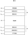
図3は比較例に係る液晶表示装置の構造を示す断面模式図である。比較例に係る液晶表示装置は、配向膜13をTFT基板10と液晶層30の間および対向基板20と液晶層30の間に有する。配向膜13は配向成分131と低抵抗成分132の2層構造になっている。配向膜13に低抵抗成分を含むため、透過率を低下させている。本明細書では、配向膜が2層構成と記載されているが、完全に2層に分離しない場合も存在する。つまり、配向膜13は、配向成分131と低抵抗成分132を有するが、それらが明確に境界をもって層分離しておらず、各成分の構成比が厚み方向にわたって変化するような場合もあり、たとえば、液晶側の最表面はほとんどが配向膜成分であるが、厚み方向にしたがって配向成分131と低抵抗成分132が共存している場合もある。本願明細書ではこのような場合であっても2層構成と表現するものとする。
FIG. 3 is a schematic cross-sectional view showing the structure of a liquid crystal display device according to a comparative example. The liquid crystal display device according to the comparative example has the
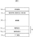
図4は実施の形態に係る液晶表示装置の構造を示す断面模式図である。実施の形態に係る液晶表示装置は、配向膜13をTFT基板10と液晶層30の間に、配向膜14を対向基板20と液晶層30の間に有する。配向膜14は、配向膜13と異なり、電気特性に制約のない配向膜である。
FIG. 4 is a schematic cross-sectional view showing the structure of the liquid crystal display device according to the embodiment. The liquid crystal display device according to the embodiment includes the
横電界方式の液晶装置では、低抵抗成分を要求されるのはTFT基板側であることから、TFT基板側に低抵抗成分を有する配向膜を使用し、対向基板側は電気特性に制約のない配向膜を使用することで、透過率を改善することができる。 In a horizontal electric field type liquid crystal device, a low resistance component is required on the TFT substrate side, so an alignment film having a low resistance component is used on the TFT substrate side, and there is no restriction on the electrical characteristics on the counter substrate side. By using the alignment film, the transmittance can be improved.
以下の実施例では、横電界方式、つまり、IPS方式の液晶表示装置を例に説明するが、それに限定されるものではなく、FFS方式等の全てのIPS方式の横電界の液晶表示装置に適用することができる。 In the following embodiments, a horizontal electric field type, that is, an IPS type liquid crystal display device will be described as an example. However, the present invention is not limited to this, and is applicable to all IPS type horizontal electric field liquid crystal display devices such as an FFS type. can do.
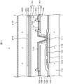
図1は実施例に係る液晶表示装置の表示領域における構造を示す断面図である。液晶表示装置1はIPS方式の液晶表示装置であり、その構造は、平面ベタで形成された対向電極108の上に絶縁膜を挟んで櫛歯状の画素電極110が形成されている。そして、画素電極110と対向電極(コモン電極ともいう)108の間の電圧によって液晶分子301を回転させることによって画素毎に液晶層300の光の透過率を制御することにより画像を形成するものである。以下に図1の構造を詳しく説明する。なお、本実施例では、図1の構成を例にとって説明するが、図1以外の液晶表示装置にも適用することができる。
FIG. 1 is a cross-sectional view illustrating a structure in a display region of a liquid crystal display device according to an embodiment. The liquid
図1において、ガラスで形成されるTFT基板100の上に、ゲート電極101が形成されている。ゲート電極101は走査線と同層の金属層で形成されている。ゲート電極101はSiNで形成される絶縁膜102に覆われている。絶縁膜102の上に、ゲート電極101と対向する位置に半導体層103が形成されている。半導体層103はTFTのチャネル部を形成するが、チャネル部を挟んで半導体層103上にソース電極104とドレイン電極105が形成される。ソース電極104は映像信号線が兼用し、ドレイン電極105は画素電極110と接続される。ソース電極104もドレイン電極105も同層の金属層で同時に形成される。
In FIG. 1, a
TFTはSINで形成される無機パッシベーション膜106に覆われている。無機パッシベーション膜106はTFTの、特にチャネル部を不純物から保護する。無機パッシベーション膜106の上にはポリイミド樹脂等の有機パッシベーション膜107が形成される。有機パッシベーション膜107はTFTの保護と同時に表面を平坦化する役割も有するので、厚く形成される。有機パッシベーション膜107の上には対向電極108が形成される。対向電極108はSiNで形成される絶縁膜109に覆われている。絶縁膜109およびスルーホール111を覆うように画素電極110が形成される。スルーホール111において、TFTから延在してきたドレイン電極105と画素電極110が導通し、映像信号が画素電極110に供給されることになる。対向電極108および画素電極110は透明導電膜であるITOで形成される。尚、無機パッシベーション膜と有機パッシベーション膜とを設けることとしているが、無機パッシベーション膜のみ、或いは、有機パッシベーション膜のみを設ける構成であってもよい。また、TFT基板上に形成されたゲート電極上に半導体層を設けるボトムゲートの構成を開示しているが、TFT基板上に半導体層を設け、半導体層上にゲート電極を設けるトップゲートの構成であってもよい。
The TFT is covered with an
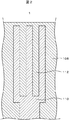
図2に画素電極110の1例を示す。画素電極110は、櫛歯状の電極である。櫛歯と櫛歯の間にスリット112が形成されている。画素電極110の下方には、平面状の対向電極108が形成されている。画素電極110に映像信号が印加されると、スリット112を通して対向電極108との間に生ずる電界によって液晶分子301が回転する。これによって液晶層300を通過する光を制御して画像を形成する。
FIG. 2 shows an example of the
図1はこの様子を断面図として説明したものである。櫛歯状の電極と櫛歯状の電極の間は図1に示すスリット112となっている。対向電極108には一定電圧が印加され、画素電極110には映像信号による電圧が印加される。画素電極110に電圧が印加されると図1に示すように、電気力線が発生して液晶分子301を電気力線の方向に回転させてバックライトからの光の透過を制御する。画素毎にバックライトからの透過が制御されるので、画像が形成されることになる。
FIG. 1 illustrates this as a cross-sectional view. A
図1の例では、有機パッシベーション膜107の上に、面状に形成された対向電極108が配置され、絶縁膜109の上に櫛歯電極110が配置されている。しかしこれとは逆に、有機パッシベーション膜107の上に面状に形成された画素電極110を配置し、絶縁膜109の上に櫛歯状の対向電極108が配置される場合もある。
In the example of FIG. 1, the
画素電極110の上には液晶分子301を配向させるための配向膜113が形成されている。本実施例においては、配向膜113は、液晶層300と接する光配向成分1131と、光配向成分1131の下層(TFT基板側)に形成される低抵抗成分1132の2層構造となっている。光配向成分1131がポリアミド酸エステルで、低抵抗成分1132がポリアミド酸で構成される。
An
図1において、液晶層300を挟んで対向基板200が設置されている。対向基板200の内側には、カラーフィルタ201が形成されている。カラーフィルタ201は画素毎に、赤、緑、青のカラーフィルタ201が形成れており、カラー画像が形成される。カラーフィルタ201とカラーフィルタ201の間にはブラックマトリクス202が形成され、画像のコントラストを向上させている。なお、ブラックマトリクス202はTFTの遮光膜としての役割も有し、TFTに光電流が流れることを防止している。
In FIG. 1, a
カラーフィルタ201およびブラックマトリクス202を覆ってオーバーコート膜203が形成されている。カラーフィルタ201およびブラックマトリクス202の表面は凹凸となっているために、オーバーコート膜203によって表面を平らにしている。
An
オーバーコート膜203の上には、液晶の初期配向を決めるための配向膜114が形成されている。対向基板側の配向膜114もTFT基板側の配向膜113と異なり、液晶層300と接する光配向成分1131と、光配向成分1131の下層(対向基板側)に形成される高抵抗成分1142の2層構造となっている。なお、液晶表示装置1はIPS方式であるから、対向電極108はTFT基板100側に形成されており、対向基板200側には形成されていない。
On the
図1に示すように、IPSでは、対向基板200の内側には導電膜が形成されていない。そうすると、対向基板200の電位が不安定になる。また、外部からの電磁ノイズが液晶層300に侵入し、画像に対して影響を与える。このような問題を除去するために、対向基板200の外側に表面導電膜210が形成される。
As shown in FIG. 1, in IPS, a conductive film is not formed inside the
ポリアミド酸エステルとポリアミド酸をブレンドワニスした光配向膜材料をTFT基板100上に印刷し、上下に2層分離、光照射、加熱イミド化等の処理を施して配向膜113が成膜される。なお、ポリアミド酸はポリアミド酸エステルに比較して極性が高くITO(Indium Tin Oxide)や有機パッシベーション膜と馴染みやすいので、常にポリアミド酸1132が下層、ポリアミド酸エステル1131が上層となる。ここで、ポリアミド酸エステル1131は配向成分で、ポリアミド酸1132は低抵抗成分である。
A photo-alignment film material obtained by blending varnish of polyamic acid ester and polyamic acid is printed on the
ポリアミド酸エステルとポリアミド酸をブレンドワニスした光配向膜材料をCF基板200上に印刷し、上下に2層分離、光照射、加熱イミド化等の処理を施して配向膜114が成膜される。ポリアミド酸1142が下層、ポリアミド酸エステル1131が上層となる。ここで、ポリアミド酸エステル1131は配向成分で、ポリアミド酸1142は高抵抗成分である。
A photo-alignment film material obtained by blending varnish of polyamic acid ester and polyamic acid is printed on the
対向基板側の配向膜114の下層に透過率の高い高抵抗成分1142が形成されるため、TFT基板側の配向膜113よりも1.5%〜3%程度透過率が高くなる。
Since the
尚、対向基板側の配向膜は、光配向成分と高抵抗成分とからなる2層の配向膜を開示しているが、高抵抗成分のみの1層構成でもよい。この場合の高抵抗、低抵抗は、TFT基板の配向膜の低抵抗成分を基準としている。対向基板の配向膜を高抵抗成分の1層のみとした場合、TFT基板や対向基板の光配向成分であるポリアミド酸エステルを使用してもよく、或いは、光配向機能を有する高抵抗成分からなるポリアミド酸を使用してもよい。また、より透過率を高めるため、対向基板側の配向膜の膜厚をTFT基板側の配向膜の膜厚よりも小さくしてもよい。また、TFT側の配向膜は、低抵抗配向膜の1層構成でもよい。 The alignment film on the counter substrate side discloses a two-layer alignment film composed of a photo-alignment component and a high-resistance component, but it may have a single-layer configuration including only a high-resistance component. The high resistance and low resistance in this case are based on the low resistance component of the alignment film of the TFT substrate. When the alignment film of the counter substrate is only one layer of the high resistance component, a polyamic acid ester that is a photo alignment component of the TFT substrate or the counter substrate may be used, or it is made of a high resistance component having a photo alignment function. Polyamic acid may be used. In order to further increase the transmittance, the thickness of the alignment film on the counter substrate side may be smaller than the thickness of the alignment film on the TFT substrate side. In addition, the alignment film on the TFT side may have a single layer structure of a low resistance alignment film.
TFT基板側と対向基板側の配向膜は、光配向成分を有する光配向膜としているが、光配向成分をラビング用の配向成分とした配向膜であってもよい。例えば、TFT基板に光配向成分と低抵抗成分とからなる配向膜を使用し、対向基板にラビング用の配向成分と高抵抗成分とからなる2層の配向膜を使用してもよい。この場合であっても、ラビング用の配向成分もTFT基板の低抵抗成分よりも高抵抗であることが望ましい。また、高抵抗成分からなる1層のラビング用の配向膜を使用してもよい。ラビング用の配向成分、高抵抗成分としては、ポリアミド酸を用いることが可能である。TFT基板を光配向とすることにより、表面段差の大きいTFT基板であっても、段差の陰になる部分まで十分に配向させることが可能となる。このとき対向基板にラビング配向膜を全面に塗布し、TFT基板に光配向膜をシール剤と重ならないように塗布することが望ましい。ラビング配向膜はシール材と接着性がよい。 The alignment film on the TFT substrate side and the counter substrate side is a photo-alignment film having a photo-alignment component, but may be an alignment film having the photo-alignment component as an alignment component for rubbing. For example, an alignment film composed of a photo-alignment component and a low resistance component may be used for the TFT substrate, and a two-layer alignment film composed of a rubbing alignment component and a high resistance component may be used for the counter substrate. Even in this case, it is desirable that the alignment component for rubbing has a higher resistance than the low resistance component of the TFT substrate. Alternatively, a single-layer rubbing alignment film made of a high resistance component may be used. Polyamide acid can be used as the rubbing alignment component and the high resistance component. By making the TFT substrate photo-aligned, even a TFT substrate having a large surface step can be sufficiently aligned up to the shadowed portion of the step. At this time, it is desirable to apply the rubbing alignment film on the entire surface of the counter substrate and apply the photo alignment film to the TFT substrate so as not to overlap the sealing agent. The rubbing alignment film has good adhesion to the sealing material.
印刷工程による配向膜切り替えは、タクトタイムが遅くなることから、配向膜の形成領域に応じて、TFT基板側の配向膜はフレキソ印刷にて塗布し、対向基板側の配向膜はインクジェットやスピンコートで塗布してもよいし、逆にTFT基板側の配向膜をインクジェットで塗布し、対向基板側の配向膜を印刷にて塗布してもよい。 Switching the alignment film in the printing process slows down the tact time, so the alignment film on the TFT substrate side is applied by flexographic printing, and the alignment film on the counter substrate side is inkjet or spin-coated, depending on the formation region of the alignment film. Alternatively, the alignment film on the TFT substrate side may be applied by inkjet, and the alignment film on the counter substrate side may be applied by printing.
以上、本発明者によってなされた発明を実施の形態および実施例に基づき具体的に説明したが、本発明は、上記実施の形態および実施例に限定されるものではなく、種々変更可能であることはいうまでもない。 Although the invention made by the present inventor has been specifically described based on the embodiments and examples, the present invention is not limited to the above-described embodiments and examples, and can be variously changed. Needless to say.
10・・・TFT基板
13・・・配向膜
131・・・配向成分
132・・・低抵抗成分
14・・・電気的に制約のない配向膜
20・・・対向基板
21・・・ポリアミド酸エステル
22・・・ポリアミド酸
100・・・TFT基板
101・・・ゲート電極
102・・・絶縁膜
103・・・半導体層
104・・・ソース電極
105・・・ドレイン電極
106・・・無機パッシベーション膜
107・・・有機パッシベーション膜
108・・・対向電極
109・・・絶縁膜
110・・・画素電極
111・・・スルーホール
112・・・スリット
113・・・配向膜
114・・・配向膜
200・・・対向基板
201・・・カラーフィルタ
202・・・ブラックマトリクス
203・・・オーバーコート膜
210・・・表面導電膜
300・・・液晶層
301・・・液晶分子
1131・・・光配向成分
1132・・・低抵抗成分
1141・・・光配向成分
1142・・・高抵抗成分
DESCRIPTION OF
Claims (10)
TFT基板と、
対向基板と
液晶層と、
前記TFT基板と前記液晶層の間に配置された第1配向膜と、
前記対向基板と前記液晶層の間に配置された第2配向膜と
を具備し、
前記第1配向膜は光配向成分と該光配向成分の抵抗よりも低い低抵抗成分とを有し、
前記第2配向膜の透過率は前記第1配向膜の透過率よりも大きい。 Liquid crystal display
A TFT substrate;
A counter substrate, a liquid crystal layer,
A first alignment film disposed between the TFT substrate and the liquid crystal layer;
A second alignment film disposed between the counter substrate and the liquid crystal layer;
The first alignment film has a photo-alignment component and a low-resistance component lower than the resistance of the photo-alignment component,
The transmittance of the second alignment film is greater than the transmittance of the first alignment film.
前記第1配向膜の光配向成分がポリアミド酸エステルであり、かつ前記第1配向膜の低抵抗成分がポリアミド酸である。 The liquid crystal display device according to claim 1.
The photo-alignment component of the first alignment film is a polyamic acid ester, and the low-resistance component of the first alignment film is a polyamic acid.
前記第2配向膜は前記第1配向膜の低抵抗成分よりも高抵抗の成分を有する。 The liquid crystal display device according to claim 2.
The second alignment film has a higher resistance component than the low resistance component of the first alignment film.
前記第2配向膜の高抵抗成分が光配向された膜である。 The liquid crystal display device according to claim 3.
The high-resistance component of the second alignment film is a photo-aligned film.
前記第2配向膜の高抵抗成分はポリアミド酸エステルである。 The liquid crystal display device according to claim 4.
The high resistance component of the second alignment film is a polyamic acid ester.
前記第2配向膜がラビング処理された配向膜である。 The liquid crystal display device according to claim 3.
The second alignment film is a rubbed alignment film.
前記第1配向膜はフレキソ印刷法で塗布した配向膜であり、前記第2配向膜はインクジェットで塗布した配向膜である。 The liquid crystal display device according to claim 3.
The first alignment film is an alignment film applied by a flexographic printing method, and the second alignment film is an alignment film applied by inkjet.
前記第1配向膜はインクジェットで塗布された膜であり、前記第2配向膜はフレキソ印刷で塗布した配向膜である。 The liquid crystal display device according to claim 3.
The first alignment film is a film applied by inkjet, and the second alignment film is an alignment film applied by flexographic printing.
前記第2配向膜は2層になっている配向膜である。 The liquid crystal display device according to claim 3.
The second alignment film is an alignment film having two layers.
前記光配向成分と前記低抵抗成分とは2層に層分離されている。 The liquid crystal display device according to claim 1.
The photo-alignment component and the low resistance component are separated into two layers.
Priority Applications (2)
| Application Number | Priority Date | Filing Date | Title |
|---|---|---|---|
| JP2013254208A JP2015114377A (en) | 2013-12-09 | 2013-12-09 | Liquid crystal display device |
| US14/564,131 US20150160516A1 (en) | 2013-12-09 | 2014-12-09 | Liquid crystal display device |
Applications Claiming Priority (1)
| Application Number | Priority Date | Filing Date | Title |
|---|---|---|---|
| JP2013254208A JP2015114377A (en) | 2013-12-09 | 2013-12-09 | Liquid crystal display device |
Publications (1)
| Publication Number | Publication Date |
|---|---|
| JP2015114377A true JP2015114377A (en) | 2015-06-22 |
Family
ID=53271027
Family Applications (1)
| Application Number | Title | Priority Date | Filing Date |
|---|---|---|---|
| JP2013254208A Pending JP2015114377A (en) | 2013-12-09 | 2013-12-09 | Liquid crystal display device |
Country Status (2)
| Country | Link |
|---|---|
| US (1) | US20150160516A1 (en) |
| JP (1) | JP2015114377A (en) |
Cited By (1)
| Publication number | Priority date | Publication date | Assignee | Title |
|---|---|---|---|---|
| KR20180069015A (en) | 2015-12-16 | 2018-06-22 | 코니카 미놀타 가부시키가이샤 | A mold- |
Family Cites Families (5)
| Publication number | Priority date | Publication date | Assignee | Title |
|---|---|---|---|---|
| EP1375562A4 (en) * | 2000-12-26 | 2005-11-30 | Nissan Chemical Ind Ltd | Diaminobenzene derivatives, polyimide precursors and polyimides prepared by using tha same, and liquid crystal aligning agents |
| JP4693186B2 (en) * | 2007-12-28 | 2011-06-01 | 株式会社 日立ディスプレイズ | Liquid crystal display |
| JP5355970B2 (en) * | 2008-09-16 | 2013-11-27 | 株式会社ジャパンディスプレイ | Liquid crystal display |
| JP5184492B2 (en) * | 2009-11-19 | 2013-04-17 | 株式会社ジャパンディスプレイイースト | Liquid crystal display device and manufacturing method thereof |
| JP5222864B2 (en) * | 2010-02-17 | 2013-06-26 | 株式会社ジャパンディスプレイイースト | Manufacturing method of liquid crystal display device |
-
2013
- 2013-12-09 JP JP2013254208A patent/JP2015114377A/en active Pending
-
2014
- 2014-12-09 US US14/564,131 patent/US20150160516A1/en not_active Abandoned
Cited By (1)
| Publication number | Priority date | Publication date | Assignee | Title |
|---|---|---|---|---|
| KR20180069015A (en) | 2015-12-16 | 2018-06-22 | 코니카 미놀타 가부시키가이샤 | A mold- |
Also Published As
| Publication number | Publication date |
|---|---|
| US20150160516A1 (en) | 2015-06-11 |
Similar Documents
| Publication | Publication Date | Title |
|---|---|---|
| US8427624B2 (en) | Liquid crystal display device | |
| US8797496B2 (en) | Liquid crystal display device | |
| US20160274428A1 (en) | Display device and method of manufacturing the same | |
| JP2015114374A (en) | Liquid crystal display device | |
| JP2015087600A (en) | Liquid crystal display device | |
| JP2009186869A (en) | Liquid crystal display device | |
| JP6591194B2 (en) | Liquid crystal display device | |
| US20170115532A1 (en) | Display panel, photo-alignment film and fabrication method thereof | |
| US10578924B2 (en) | Orientation film materials and liquid crystal display device using it | |
| JP2017067830A (en) | Display device | |
| US9829759B2 (en) | Liquid crystal display device | |
| JP2015135411A (en) | Liquid crystal display | |
| JP2016014779A (en) | Liquid crystal display device | |
| US20150212373A1 (en) | Liquid crystal display device | |
| US20180017832A1 (en) | Liquid crystal display device | |
| JP2016015404A (en) | Liquid crystal display device | |
| JP2015114377A (en) | Liquid crystal display device | |
| TWI675241B (en) | Liquid crystal display device | |
| CN105319791A (en) | Liquid crystal display device | |
| KR20080068778A (en) | Liquid Crystal Display Panel With Ion Capture Structure And Liquid Crystal Display Device Including The Same | |
| JP7201777B2 (en) | liquid crystal display | |
| US9588366B2 (en) | Liquid crystal display device comprising a capacitance insulating film having a thickness and a dielectric constant | |
| JP6150684B2 (en) | Liquid crystal display device and array substrate | |
| JP6980730B2 (en) | Liquid crystal display device | |
| JP4441507B2 (en) | Liquid crystal display |