JP2015114243A - Testing device and method; and program - Google Patents
Testing device and method; and program Download PDFInfo
- Publication number
- JP2015114243A JP2015114243A JP2013257365A JP2013257365A JP2015114243A JP 2015114243 A JP2015114243 A JP 2015114243A JP 2013257365 A JP2013257365 A JP 2013257365A JP 2013257365 A JP2013257365 A JP 2013257365A JP 2015114243 A JP2015114243 A JP 2015114243A
- Authority
- JP
- Japan
- Prior art keywords
- lower limit
- search
- test
- limit value
- determined
- Prior art date
- Legal status (The legal status is an assumption and is not a legal conclusion. Google has not performed a legal analysis and makes no representation as to the accuracy of the status listed.)
- Granted
Links
Images


Landscapes
- Tests Of Electronic Circuits (AREA)
- Testing Or Measuring Of Semiconductors Or The Like (AREA)
Abstract
Description
本発明は、電子デバイスの試験装置及び方法、並びにプログラムに関する。 The present invention relates to an electronic device testing apparatus and method, and a program.
電子デバイスである半導体チップのpass/failを判定する試験の一つに、機能試験(ファンクションテスト)がある。ファンクションテストでは、回路推奨の動作使用電圧で試験パターンを半導体チップの集積回路に印加し、要求仕様を満たしているか否かで、半導体チップ毎にpass/failの判定を行っている。 One of the tests for determining pass / fail of a semiconductor chip that is an electronic device is a function test. In the function test, a test pattern is applied to an integrated circuit of a semiconductor chip with a circuit-recommended operating voltage, and pass / fail is determined for each semiconductor chip depending on whether the required specifications are satisfied.
被試験対象である半導体チップには、デバイス保障温度が低温(例えば−40℃等)まで含まれるものがある。この場合には、高温(又は室温)におけるファンクションテストに加えて、低温におけるファンクションテストも実行することを要する。温度特性又は経時劣化特性を持つ半導体チップでは、高温ではpassと判定されるが、低温ではfailと判定されるものがある。このような半導体チップでは、高温と併せて低温でもファンクションテストを行わなければ、不良品の検出をすることができない。 Some semiconductor chips to be tested include device guarantee temperatures up to low temperatures (eg, −40 ° C.). In this case, it is necessary to execute a function test at a low temperature in addition to a function test at a high temperature (or room temperature). Some semiconductor chips having temperature characteristics or aging deterioration characteristics are determined to be pass at high temperatures but determined to be fail at low temperatures. In such a semiconductor chip, a defective product cannot be detected unless a function test is performed at a low temperature in addition to a high temperature.
このように、被試験対象が温度特性又は経時劣化特性を持つ半導体チップである場合には、複数の異なる温度でファンクションテストを行うことを必要とし、試験工数の増大や試験コスト増を招来するという課題がある。 As described above, when the object to be tested is a semiconductor chip having temperature characteristics or aging deterioration characteristics, it is necessary to perform a function test at a plurality of different temperatures, which increases test man-hours and test costs. There are challenges.
本発明は、上記の課題に鑑みてなされたものであり、温度特性又は経時劣化特性を持つ電子デバイスについて、試験工数を削減して試験コストの低減を実現するも、良品又は不良品の正確な判定を可能とする試験装置及び方法を提供することを目的とする。 The present invention has been made in view of the above problems, and for electronic devices having temperature characteristics or aging deterioration characteristics, the test man-hours can be reduced to reduce the test cost. It is an object of the present invention to provide a test apparatus and method that enable determination.
試験装置の一態様は、複数の電子デバイスについて、前記電子デバイス毎に所定温度における機能試験を行う試験装置であって、前記機能試験に際して、前記電子デバイス毎に電圧又は周波数の動作下限値を決定する決定部と、決定された前記動作下限値を集計して分布を算出する演算部と、算出された前記分布を用いて、前記電子デバイスについて良品又は不良品の判定を行う判定部とを含む。 One aspect of the test apparatus is a test apparatus that performs a function test at a predetermined temperature for each of the plurality of electronic devices. In the function test, an operation lower limit value of voltage or frequency is determined for each of the electronic devices. A determination unit that calculates the distribution by aggregating the determined operation lower limit values, and a determination unit that determines a non-defective product or a defective product for the electronic device using the calculated distribution. .
試験方法の一態様は、複数の電子デバイスについて、前記電子デバイス毎に所定温度における機能試験を行うに際して、前記電子デバイス毎に電圧又は周波数の動作下限値を決定する工程と、決定された前記動作下限値を集計して分布を算出する工程と、算出された前記分布を用いて、前記電子デバイスについて良品又は不良品の判定を行う工程とを含む。 One aspect of the test method is the step of determining an operation lower limit value of voltage or frequency for each electronic device when performing a function test at a predetermined temperature for each of the electronic devices, and the determined operation A step of calculating a distribution by counting the lower limit values, and a step of determining a non-defective product or a defective product for the electronic device using the calculated distribution.
プログラムの一態様は、複数の電子デバイスについて、前記電子デバイス毎に所定温度における機能試験を行うに際して、前記電子デバイス毎に電圧又は周波数の動作下限値を決定する手順と、決定された前記動作下限値を集計して分布を算出する手順と、算出された前記分布を用いて、前記電子デバイスについて良品又は不良品の判定を行う手順とをコンピュータに実行させるためのものである。 One aspect of the program is a procedure for determining an operation lower limit value of voltage or frequency for each electronic device when performing a function test at a predetermined temperature for each of the electronic devices, and the determined operation lower limit. This is for causing a computer to execute a procedure for calculating a distribution by collecting values and a procedure for determining a non-defective product or a defective product for the electronic device using the calculated distribution.
本発明によれば、温度特性又は経時劣化特性を持つ電子デバイスについて、試験工数を削減して試験コストの低減を実現するも、良品又は不良品の正確な判定を行うことが可能となる。 According to the present invention, for an electronic device having temperature characteristics or aging deterioration characteristics, it is possible to accurately determine a non-defective product or a defective product while reducing the test man-hour and reducing the test cost.
以下の諸実施形態では、電子デバイスとして半導体チップを例示し、半導体チップの試験装置及び試験方法を開示する。 In the following embodiments, a semiconductor chip is exemplified as an electronic device, and a semiconductor chip test apparatus and test method are disclosed.
(第1の実施形態)
先ず、第1の実施形態について説明する。
図1は、本実施形態による試験システムを示すブロック図である。図2は、本実施形態による試験方法をステップ順に示すフロー図である。
(First embodiment)
First, the first embodiment will be described.
FIG. 1 is a block diagram showing a test system according to the present embodiment. FIG. 2 is a flowchart showing the test method according to this embodiment in the order of steps.
この試験システムは、図1に示すように、テスタ1、プローブ2、コンピュータ3、及び最終判定サーバ4を備えて構成される。
テスタ1は、試験プログラム10に従って、半導体チップの機能試験(ファンクションテスト)を行うものであり、ファンクションテストの際に通常試験と共に後述する下限電圧サーチを実行する。これにより、動作下限値として動作下限電圧値が決定される。テスタ1は、試験プログラム10の実行により動作下限電圧値を決定する決定部11と、HDD等のデータ格納部12とを備えている。
プローブ2は、テスタ1と接続されており、試験プログラム10に基づいて半導体チップの接続端子に接触してファンクションテストを実行する。
As shown in FIG. 1, the test system includes a
The
The
コンピュータ3は、演算部13及び判定部14を備えている。
演算部13は、ファンクションテストの際に半導体チップ毎に決定された動作下限電圧値を集計し、動作下限電圧値の中央値又は平均値及び動作下限電圧値の分布を算出する。
判定部14は、算出された分布を用いて、設定された基準により半導体チップについて良品又は不良品の判定を行う。
The
The
The determination unit 14 uses the calculated distribution to determine whether the semiconductor chip is a non-defective product or a defective product based on a set reference.
最終判定サーバ4は、通常試験の結果と、判定部14による良品又は不良品の判定結果とを合わせて、半導体ウェーハにおける良品半導体チップを決定する。 The final determination server 4 determines the non-defective semiconductor chip in the semiconductor wafer by combining the result of the normal test and the determination result of the non-defective product or the defective product by the determination unit 14.
以下、上記の試験システムを用いた半導体チップの試験方法について、図2を用いて説明する。
本実施形態では、図3に示すように、複数(例えば数百個)の半導体チップがマトリクス状に並んで形成されてなる半導体ウェーハを被試験対象とする。
Hereinafter, a semiconductor chip test method using the above test system will be described with reference to FIG.
In the present embodiment, as shown in FIG. 3, a semiconductor wafer in which a plurality of (for example, several hundred) semiconductor chips are formed in a matrix is used as a test object.
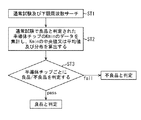
テスタ1は、試験プログラム10に従って、通常試験及びそれと共に下限電圧サーチを行う(ステップST1)。下限電圧サーチは、詳細下限電圧サーチ及び簡易下限電圧サーチからなる。
ステップST1として、詳細下限電圧サーチを含むフローを図4−1に、簡易下限電圧サーチを含むフローを図5−1にそれぞれ示す。
The
As step ST1, a flow including a detailed lower limit voltage search is shown in FIG. 4-1, and a flow including a simple lower limit voltage search is shown in FIG. 5-1.
図4−1に示すように、図3に示す複数(例えば数百個)の半導体チップのうち、初めの数十個(1〜N番目までのN個とする)について、通常試験及び詳細下限電圧サーチが実行される。
半導体ウェーハに形成された各半導体チップについて順次に、プローブ2を接続端子に接触して、試験プログラム10に基づいて、高温又は常温において、通常試験を実行する(ステップST11)。通常試験は、試験周波数k=1(相対値)における動作使用電圧(通常試験ポイント)により行われる。図6は、半導体デバイス評価或いはデバイス調査時に一時的に取得される動作電圧と動作周波数との関係を表すshmoo図であり、本願発明を説明のために示すものである。
As shown in FIG. 4A, the normal test and the lower limit of detail for the first several dozen (several hundreds) semiconductor chips shown in FIG. A voltage search is performed.
For each semiconductor chip formed on the semiconductor wafer, the
ステップST11で取得した通常試験の結果を判定する(ステップST12)。ステップST11で試験結果がfailのときには、当該半導体チップは不良品であると判定され、当該半導体チップの試験を終了する(ステップST13)。試験結果がpassのときには、ステップST21に進む。各半導体チップについての通常試験の判定結果のデータは、データ格納部12に格納される。
The result of the normal test acquired in step ST11 is determined (step ST12). When the test result is “fail” in step ST11, it is determined that the semiconductor chip is defective, and the test of the semiconductor chip is finished (step ST13). When the test result is pass, the process proceeds to step ST21. The data of the determination result of the normal test for each semiconductor chip is stored in the
図4−1のステップST21〜ST25では、試験プログラム10に基づいて詳細下限電圧サーチが実行される。詳細下限電圧サーチのイメージを図4−2に示す。詳細下限電圧サーチは、試験温度により特に顕著な差異が見られる試験周波数k=1(相対値)において行われる。
ステップST21では、図6のようなサーチ下限電圧(SL)及びサーチ上限電圧(SU)を用いてS1(=(SL+SU)/2)を算出し、S1におけるpass/failを判定する。SUは、通常試験の動作使用電圧とする。
In steps ST21 to ST25 of FIG. 4A, a detailed lower limit voltage search is executed based on the
In step ST21, S1 (= (SL + SU) / 2) is calculated using the search lower limit voltage (SL) and the search upper limit voltage (SU) as shown in FIG. 6, and pass / fail in S1 is determined. SU is the operating voltage for normal testing.
続いて、ステップST22を実行する。ステップST22では、S1の判定結果がpassである場合には、S1及びSLを用いてS2(=(S1+SL)/2)を算出し、S2におけるpass/failを判定する。S2の判定結果がfailである場合には、S1及びSUを用いてS2(=(S1+SU)/2)を算出し、S2におけるpass/failを判定する。 Subsequently, step ST22 is executed. In step ST22, when the determination result of S1 is pass, S2 (= (S1 + SL) / 2) is calculated using S1 and SL, and pass / fail in S2 is determined. If the determination result of S2 is fail, S2 (= (S1 + SU) / 2) is calculated using S1 and SU, and pass / fail in S2 is determined.
詳細下限電圧サーチは、最終回をM回として、M−1回との差分が最小サーチ単位(分解能により規定される)となるまで行われ、動作下限電圧値が決定されて、終了する。図4−1では、M回目のステップをST(M)と記す。
一例として、M=5の場合(更にステップST23〜ST25を行う場合)について、以下に示す。
The detailed lower limit voltage search is performed until the final count is M times, and the difference from M-1 times is the minimum search unit (defined by the resolution), the operation lower limit voltage value is determined, and is terminated. In FIG. 4A, the Mth step is denoted as ST (M).
As an example, the case where M = 5 (when steps ST23 to ST25 are further performed) is shown below.
続いて、ステップST23を実行する。ステップST23では、S1及びS2を用いてS3(=(S1+S2)/2)を算出し、S3におけるpass/failを判定する。
続いて、ステップST24を実行する。ステップST24では、S2及びS3を用いてS4(=(S2+S3)/2)を算出し、S4におけるpass/failを判定する。
続いて、ステップST25を実行する。ステップST25では、S3及びS4を用いてS5(=(S3+S4)/2)を算出し、S5におけるpass/failを判定する。
なお、ステップST(M)では、S(M−2)及びS(M−1)を用いてS(M)(=(S(M−2)+S(M−1))/2)を算出し、S(M)におけるpass/failを判定することになる。
Subsequently, step ST23 is executed. In step ST23, S3 (= (S1 + S2) / 2) is calculated using S1 and S2, and pass / fail in S3 is determined.
Subsequently, step ST24 is executed. In step ST24, S4 (= (S2 + S3) / 2) is calculated using S2 and S3, and pass / fail in S4 is determined.
Subsequently, step ST25 is executed. In step ST25, S5 (= (S3 + S4) / 2) is calculated using S3 and S4, and pass / fail in S5 is determined.
In step ST (M), S (M) (= (S (M−2) + S (M−1)) / 2) is calculated using S (M−2) and S (M−1). Then, pass / fail in S (M) is determined.
具体例として、最小サーチ単位が0.0125Vであり、SLが0.8V、SUが1.2Vである場合について説明する。このとき、実際の動作下限電圧値が0.937Vであるとする。
ステップST21では、S1=(0.8+1.2)/2=1.00となり、passと判定される。
ステップST22では、S2=(1.0+0.8)/2=0.90となり、failと判定される。差分(S2−S1)は0.1Vとなる。
ステップST23では、S3=(0.9+1.0)/2=0.95となり、passと判定される。差分(S2−S1)は0.05Vとなる。
ステップST24では、S4=(0.95+0.9)/2=0.925となり、failと判定される。差分(S3−S2)は0.025Vとなる。
ステップST25では、S5=(0.925+0.95)/2=0.9375となり、passと判定される。差分(S3−S2)は0.0125Vとなる。差分が最小サーチ単位に達したことから、動作下限電圧値は、ステップST25において0.9375Vと決定される。
As a specific example, a case where the minimum search unit is 0.0125V, SL is 0.8V, and SU is 1.2V will be described. At this time, it is assumed that the actual operation lower limit voltage value is 0.937V.
In step ST21, S1 = (0.8 + 1.2) /2=1.00, and it is determined as pass.
In step ST22, S2 = (1.0 + 0.8) /2=0.90, and it is determined as fail. The difference (S2-S1) is 0.1V.
In step ST23, S3 = (0.9 + 1.0) /2=0.95, which is determined to be pass. The difference (S2-S1) is 0.05V.
In step ST24, S4 = (0.95 + 0.9) /2=0.925, and it is determined as fail. The difference (S3-S2) is 0.025V.
In step ST25, S5 = (0.925 + 0.95) /2=0.9375, and it is determined as pass. The difference (S3-S2) is 0.0125V. Since the difference has reached the minimum search unit, the operation lower limit voltage value is determined to be 0.9375 V in step ST25.
詳細下限電圧サーチでは、初めの1〜N番目までの半導体チップの各々について、ステップST11〜ST13及びST21〜ST(M)を順次行い、ステップST14において、半導体チップ毎の動作下限電圧値を決定する。以下、動作下限電圧値をVminと記載する。Vminのデータはデータ格納部12に格納される。
In the detailed lower limit voltage search, steps ST11 to ST13 and ST21 to ST (M) are sequentially performed for each of the first to Nth semiconductor chips, and in step ST14, an operation lower limit voltage value for each semiconductor chip is determined. . Hereinafter, the operation lower limit voltage value is described as V min . The data of V min is stored in the
詳細下限電圧サーチの後、その他の試験を行い(ステップST15)、図5−1に示すように、演算部13は、初めの1〜N番目までの半導体チップについて詳細下限電圧サーチで決定された各Vminの中央値又は平均値を算出する(ステップST31)。この中央値又は平均値をSAとする。1〜N番目までのN個の半導体チップのうち、所定の半導体チップが他の半導体チップに比べてVminが比較的大きく外れた値となることが想定されるため、SAは中央値を採用することが望ましい。
After the detailed lower limit voltage search, other tests are performed (step ST15). As shown in FIG. 5A, the
詳細下限電圧サーチの対象となった半導体チップ以外の残りの((N+1)番目〜最後までの)半導体チップについて、通常試験及び簡易下限電圧サーチが実行される。
半導体ウェーハに形成された各半導体チップについて順次に、プローブ2を接続端子に接触して、試験プログラム10に基づいて通常試験を実行する(ステップST11)。通常試験は、高温又は常温において、試験周波数k=1(相対値)における動作使用電圧により行われる。
A normal test and a simple lower limit voltage search are performed on the remaining semiconductor chips (from (N + 1) th to the last) other than the semiconductor chip that is the target of the detailed lower limit voltage search.
For each semiconductor chip formed on the semiconductor wafer, the
ステップST11で取得した通常試験の結果を判定する(ステップST12)。ステップST11で試験結果がfailのときには、当該半導体チップは不良品であると判定され、当該半導体チップの試験を終了する(ステップST13)。試験結果がpassのときには、ステップST41に進む。各半導体チップについての通常試験の判定結果のデータは、データ格納部12に格納される。
The result of the normal test acquired in step ST11 is determined (step ST12). When the test result is “fail” in step ST11, it is determined that the semiconductor chip is defective, and the test of the semiconductor chip is finished (step ST13). When the test result is pass, the process proceeds to step ST41. The data of the determination result of the normal test for each semiconductor chip is stored in the
図5−1のステップST41〜ST(M)により、試験プログラム10に基づいて簡易下限電圧サーチが実行される。詳細下限電圧サーチのイメージを図5−2〜図5−6に示す。簡易下限電圧サーチは、試験温度により特に顕著な差異が見られる試験周波数k=1(相対値)において行われる。
図5−2に示すように、ステップST41では、S1=SAにおけるpass/failを判定する。
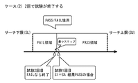
ステップST41においてS1の判定結果がfailである場合には、ステップST42に進む。ステップST42では、SA及びSUを用いてS2(=(SA+SU)/2)を算出し、S2におけるpass/failを判定する。S2の判定結果がpassである場合には、S2がVminと決定されて、簡易下限電圧サーチを終了する。この場合をケース(1)とする。
A simple lower limit voltage search is executed based on the
As shown in FIG. 5B, in step ST41, pass / fail in S1 = SA is determined.
When the determination result of S1 is “fail” in step ST41, the process proceeds to step ST42. In step ST42, S2 (= (SA + SU) / 2) is calculated using SA and SU, and pass / fail in S2 is determined. If the determination result of S2 is pass, S2 is determined to be V min and the simple lower limit voltage search is terminated. This case is referred to as case (1).
図5−3に示すように、ステップST41においてS1の判定結果がpassである場合には、ステップST43に進む。ステップST43では、SA及びSLを用いてS3(=(SA+SL)/2)を算出し、S3におけるpass/failを判定する。S3の判定結果がfailである場合には、S1(=SA)がVminと決定されて、簡易下限電圧サーチを終了する。この場合をケース(2)とする。 As illustrated in FIG. 5C, when the determination result of S1 is “pass” in step ST41, the process proceeds to step ST43. In step ST43, S3 (= (SA + SL) / 2) is calculated using SA and SL, and pass / fail in S3 is determined. When the determination result of S3 is “fail”, S1 (= SA) is determined as V min and the simple lower limit voltage search is terminated. This case is referred to as case (2).
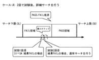
図5−4に示すように、ステップST43においてS3の判定結果がpassである場合には、ステップST44に進む。ステップST44では、S3及びSLを用いてS4(=(S3+SL)/2)を算出し、S4におけるpass/failを判定する。S4の判定結果がfailである場合には、S3がVminと決定されて、簡易下限電圧サーチを終了する。この場合をケース(3)とする。 As shown in FIG. 5-4, if the determination result in S3 is “pass” in step ST43, the process proceeds to step ST44. In step ST44, S4 (= (S3 + SL) / 2) is calculated using S3 and SL, and pass / fail in S4 is determined. If the determination result in S4 is fail, S3 is determined to be V min and the simple lower limit voltage search is terminated. This case is referred to as case (3).
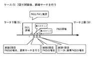
図5−5に示すように、ステップST42においてS2の判定結果がfailである場合には、簡易下限電圧サーチを終了する。この場合をケース(4)とする。その後、当該半導体チップについては、上記した詳細下限電圧サーチが実行され、Vminが決定される。 As shown in FIG. 5-5, when the determination result of S2 is “fail” in step ST42, the simple lower limit voltage search is terminated. This case is referred to as case (4). Thereafter, the detailed lower limit voltage search described above is executed for the semiconductor chip, and V min is determined.
図5−6に示すように、ステップST44においてS4の判定結果がpassである場合には、簡易下限電圧サーチを終了する。この場合をケース(5)とする。その後、当該半導体チップについては、上記した詳細下限電圧サーチが実行され、Vminが決定される。 As shown in FIG. 5-6, when the determination result of S4 is “pass” in step ST44, the simple lower limit voltage search is terminated. This case is referred to as case (5). Thereafter, the detailed lower limit voltage search described above is executed for the semiconductor chip, and V min is determined.
簡易下限電圧サーチでは、ケース(1),(2)のときには2回のサーチでVminが決定される。ケース(3)の場合には3回のサーチでVminが決定される。このように、ケース(1)〜(3)であれば、サーチに要する試験工数が削減され、試験時間の増大を抑えて試験コストの低減が実現する。一方、ケース(4),(5)の場合には詳細下限電圧サーチを要する。しかしながら後述するように、Vminが決定される半導体チップの殆ど(98%以上)がケース(1)〜(3)に該当することが確認されている。即ち、簡易下限電圧サーチを行う殆どの半導体チップがケース(1)〜(3)に該当し(98%以上)、ケース(4),(5)の場合は極稀である(2%以下)。従って、詳細下限電圧サーチと共に簡易下限電圧サーチを採用することにより、試験工数が削減され、試験時間の短縮及び試験コストの低減が実現する。 In the simple lower limit voltage search, Vmin is determined by two searches in cases (1) and (2). In case (3), V min is determined by three searches. As described above, in the cases (1) to (3), the number of test steps required for the search is reduced, and the test cost can be reduced by suppressing an increase in test time. On the other hand, in the cases (4) and (5), a detailed lower limit voltage search is required. However, as will be described later, it has been confirmed that most (98% or more) of the semiconductor chips for which V min is determined correspond to cases (1) to (3). That is, most of the semiconductor chips that perform the simple lower limit voltage search correspond to cases (1) to (3) (98% or more), and cases (4) and (5) are extremely rare (2% or less). . Therefore, by employing the simple lower limit voltage search together with the detailed lower limit voltage search, the test man-hours are reduced, and the test time and test cost can be reduced.
以上のようにして、半導体ウェーハに形成された複数の半導体チップの全てについて、ステップST1が終了する。詳細下限電圧サーチ及び簡易下限電圧サーチで取得された各半導体チップのVminのデータは、データ格納部12に格納される。その後、ステップST2に進む。
As described above, step ST1 is completed for all of the plurality of semiconductor chips formed on the semiconductor wafer. The V min data of each semiconductor chip acquired by the detailed lower limit voltage search and the simple lower limit voltage search is stored in the
ステップST2では、演算部13は、データ格納部12に格納されている各半導体チップのVminのデータを集計し、Vminの中央値又は平均値及びVminの分布(例えば6σ)を算出する。その後、ステップST3に進む。
At step ST2, the
ステップST3では、判定部14は、算出されたVmin分布を用いて、半導体ウェーハに形成された複数の半導体チップのうち、ステップST12で不良品であると判定されたものを除く全てについて、良品又は不良品の判定を行う。当該半導体チップのVminが設定された基準を満たしていれば、当該半導体チップは良品と判定される。設定された基準を満たしていない場合には、動作下限電圧異常の半導体チップであり、不良品と判定される。 In step ST3, the determination unit 14 uses the calculated Vmin distribution to determine that all of the plurality of semiconductor chips formed on the semiconductor wafer except for those determined to be defective in step ST12 are non-defective. Or, a defective product is determined. If V min of the semiconductor chip satisfies the set standard, the semiconductor chip is determined as a non-defective product. If the set standard is not satisfied, it is determined that the semiconductor chip has an abnormal operation lower limit voltage and is defective.
データ格納部12に格納されているステップST12による通常試験の判定結果のデータと、ステップST3によるVminに関する判定結果のデータとが、最終判定サーバ4に入力される。最終判定サーバ4は、双方の判定結果のデータを総合して、半導体ウェーハに形成された複数の半導体チップのうちの最終的な良品を決定する。
The determination result of the data of the normal test by step ST12 stored in the
以下、本実施形態による試験方法により奏される諸効果について調べた結果について説明する。 Hereinafter, the results of examining various effects exhibited by the test method according to the present embodiment will be described.
簡易下限電圧サーチにおけるケース(1)〜(5)の発生頻度について調べた。その結果を図7(a)に示す。図7(a)は、ロジック回路の半導体チップについて、高温(例えば85℃)において簡易下限電圧サーチで取得した半導体チップ毎のVminのヒストグラムである。ここでは、Vminの分布に対して統計処理を施し、分布から外れた(例えば6σ以上)半導体チップは、低温不良として判定した。図7(a)のように、動作下限電圧値が決定される半導体チップの殆ど(98%以上)がケース(1)〜(3)に該当することが確認された。 The occurrence frequency of cases (1) to (5) in the simple lower limit voltage search was examined. The result is shown in FIG. FIG. 7A is a histogram of V min for each semiconductor chip acquired by a simple lower limit voltage search at a high temperature (for example, 85 ° C.) for the semiconductor chip of the logic circuit. Here, statistical processing was performed on the distribution of V min, and a semiconductor chip that deviated from the distribution (for example, 6σ or more) was determined as a low temperature defect. As shown in FIG. 7A, it was confirmed that most (98% or more) of the semiconductor chips for which the operation lower limit voltage value is determined correspond to cases (1) to (3).
図7(a)で取得した高温におけるVminと共に、低温(例えば−10℃)でも同様にVminを取得し、両者のVminの関係について調べた。その結果を図7(b)に示す。図7(b)では、高温における良品/不良品判定の基準を実線で、低温における良品/不良品判定の基準を破線で示す。図7(b)のように、図7(a)で低温不良となると判定された半導体チップは、低温の試験においても不良品として検出されることが確認された。 Along with V min at a high temperature obtained in FIG. 7A, V min was similarly obtained at a low temperature (for example, −10 ° C.), and the relationship between the two V min was examined. The result is shown in FIG. In FIG. 7B, the standard for determining good / defective products at high temperatures is indicated by a solid line, and the criterion for determining good / defective products at low temperatures is indicated by a broken line. As shown in FIG. 7B, it was confirmed that the semiconductor chip determined to have a low temperature defect in FIG. 7A was detected as a defective product even in a low temperature test.
以上より、本実施形態によれば、詳細下限電圧サーチと共に簡易下限電圧サーチを採用することにより、試験工数が削減され、試験時間の短縮及び試験コストの低減が実現するも、半導体チップの良品/不良品の正確な判定を行うことができる。 As described above, according to the present embodiment, by adopting the simple lower limit voltage search together with the detailed lower limit voltage search, the test man-hours can be reduced, the test time can be shortened, and the test cost can be reduced. It is possible to accurately determine defective products.
本実施形態は、動作周波数を固定して動作下限電圧値を決定するものであって、例えば、RAMの低電圧試験やロジック回路のスキャンチェーン試験等に適用することにより、高い不良品検出精度を得ることができる。 In this embodiment, the operating lower limit voltage value is determined by fixing the operating frequency. For example, by applying it to a low voltage test of a RAM or a scan chain test of a logic circuit, high defective product detection accuracy is achieved. Can be obtained.
(第2の実施形態)
続いて、第2の実施形態について説明する。
図8は、本実施形態による判定装置を含む試験システムを示すブロック図である。図8では、図1と同じ構成要素については同符号を付す。図9は、本実施形態による試験方法をステップ順に示すフロー図である。
(Second Embodiment)
Next, the second embodiment will be described.
FIG. 8 is a block diagram showing a test system including the determination apparatus according to the present embodiment. In FIG. 8, the same components as those in FIG. FIG. 9 is a flowchart showing the test method according to this embodiment in the order of steps.
この試験システムは、第1の実施形態における図1と同様に、テスタ1、プローブ2、コンピュータ3、及び最終判定サーバ4を備えて構成される。
テスタ1は、試験プログラム20に従って、半導体チップのファンクションテストを行うものであり、ファンクションテストの際に通常試験と共に後述する下限周波数サーチを実行する。これにより、動作下限値として動作下限周波数が決定される。テスタ1は、試験プログラム20の実行により動作下限周波数を決定する決定部11と、HDD等のデータ格納部12とを備えている。
プローブ2は、テスタ1と接続されており、試験プログラム20に基づいて半導体チップの接続端子に接触してファンクションテストを実行する。
This test system is configured to include a
The
The
コンピュータ3は、演算部13及び判定部14を備えている。
演算部13は、ファンクションテストの際に半導体チップ毎に決定された動作下限周波数を集計し、動作下限周波数の中央値又は平均値及び動作下限周波数の分布を算出する。
判定部14は、算出された分布を用いて、設定された基準により半導体チップについて良品又は不良品の判定を行う。
The
The
The determination unit 14 uses the calculated distribution to determine whether the semiconductor chip is a non-defective product or a defective product based on a set reference.
最終判定サーバ4は、通常試験の結果と、判定部14による良品又は不良品の判定結果とを合わせて、半導体ウェーハにおける良品半導体チップを決定する。 The final determination server 4 determines the non-defective semiconductor chip in the semiconductor wafer by combining the result of the normal test and the determination result of the non-defective product or the defective product by the determination unit 14.
以下、上記の試験システムを用いた半導体チップの試験方法について、図9を用いて説明する。
本実施形態では、第1の実施形態と同様に、複数(例えば数百個)の半導体チップがマトリクス状に並んで形成されてなる半導体ウェーハを被試験対象とする。
Hereinafter, a semiconductor chip test method using the above test system will be described with reference to FIG.
In the present embodiment, as in the first embodiment, a semiconductor wafer in which a plurality of (for example, several hundred) semiconductor chips are formed in a matrix is used as a test object.
テスタ1は、試験プログラム10に従って、通常試験及びそれと共に下限周波数サーチを行う(ステップST1)。下限周波数サーチは、詳細下限周波数サーチ及び簡易周波数サーチからなる。
ステップST1として、詳細下限周波数サーチを含むフローを図10に、簡易下限周波数サーチを含むフローを図11にそれぞれ示す。
The
As step ST1, a flow including a detailed lower limit frequency search is shown in FIG. 10, and a flow including a simple lower limit frequency search is shown in FIG.
図10に示すように、複数(例えば数百個)の半導体チップのうち、初めの数十個(1〜N番目までのN個とする)について、通常試験及び詳細下限周波数サーチが実行される。
半導体ウェーハに形成された各半導体チップについて順次に、プローブ2を接続端子に接触して、試験プログラム20に基づいて通常試験を実行する(ステップST11)。通常試験は、高温又は常温において、例えば試験電圧v=1.08Vにおける動作使用周波数により行われる。
As shown in FIG. 10, a normal test and a detailed lower limit frequency search are performed on the first several tens (N to 1 to N) of a plurality (for example, several hundred) of semiconductor chips. .
For each semiconductor chip formed on the semiconductor wafer, the
ステップST11で取得した通常試験の結果を判定する(ステップST12)。ステップST11で試験結果がfailのときには、当該半導体チップは不良品であると判定され、当該半導体チップの試験を終了する(ステップST13)。試験結果がpassのときには、ステップST21に進む。各半導体チップについての通常試験の判定結果のデータは、データ格納部12に格納される。
The result of the normal test acquired in step ST11 is determined (step ST12). When the test result is “fail” in step ST11, it is determined that the semiconductor chip is defective, and the test of the semiconductor chip is finished (step ST13). When the test result is pass, the process proceeds to step ST21. The data of the determination result of the normal test for each semiconductor chip is stored in the
図10のステップST21〜ST25では、試験プログラム20に基づいて詳細下限周波数サーチが実行される。詳細下限周波数サーチのイメージは、第1の実施形態の図4−2と同様である。詳細下限周波数サーチは、試験温度により特に顕著な差異が見られる例えば試験電圧v=1.08Vにおいて行われる。
ステップST21では、サーチ下限周波数(SL)及びサーチ上限周波数(SU)を用いてS1(=(SL+SU)/2)を算出し、S1におけるpass/failを判定する。SUは、通常試験の動作使用周波数とする。
In steps ST <b> 21 to ST <b> 25 in FIG. 10, the detailed lower limit frequency search is executed based on the
In step ST21, S1 (= (SL + SU) / 2) is calculated using the search lower limit frequency (SL) and the search upper limit frequency (SU), and pass / fail in S1 is determined. SU is the operating frequency for normal testing.
続いて、ステップST22を実行する。ステップST22では、S1の判定結果がpassである場合には、S1及びSLを用いてS2(=(S1+SL)/2)を算出し、S2におけるpass/failを判定する。S2の判定結果がfailである場合には、S1及びSUを用いてS2(=(S1+SU)/2)を算出し、S2におけるpass/failを判定する。 Subsequently, step ST22 is executed. In step ST22, when the determination result of S1 is pass, S2 (= (S1 + SL) / 2) is calculated using S1 and SL, and pass / fail in S2 is determined. If the determination result of S2 is fail, S2 (= (S1 + SU) / 2) is calculated using S1 and SU, and pass / fail in S2 is determined.
詳細下限周波数サーチは、最終回をM回として、M−1回との差分が最小サーチ単位(分解能により規定される)となるまで行われ、動作下限周波数が決定されて、終了する。図11では、M回目のステップをST(M)と記す。
一例として、M=5の場合(更にステップST23〜ST25を行う場合)について、以下に示す。
The detailed lower limit frequency search is performed until the final count is M times, and the difference from M-1 times is the minimum search unit (defined by the resolution), the operation lower limit frequency is determined, and is terminated. In FIG. 11, the Mth step is denoted as ST (M).
As an example, the case where M = 5 (when steps ST23 to ST25 are further performed) is shown below.
続いて、ステップST23を実行する。ステップST23では、S1及びS2を用いてS3(=(S1+S2)/2)を算出し、S3におけるpass/failを判定する。
続いて、ステップST24を実行する。ステップST24では、S2及びS3を用いてS4(=(S2+S3)/2)を算出し、S4におけるpass/failを判定する。
続いて、ステップST25を実行する。ステップST25では、S3及びS4を用いてS5(=(S3+S4)/2)を算出し、S5におけるpass/failを判定する。
なお、ステップST(M)では、S(M−2)及びS(M−1)を用いてS(M)(=(S(M−2)+S(M−1))/2)を算出し、S(M)におけるpass/failを判定することになる。
Subsequently, step ST23 is executed. In step ST23, S3 (= (S1 + S2) / 2) is calculated using S1 and S2, and pass / fail in S3 is determined.
Subsequently, step ST24 is executed. In step ST24, S4 (= (S2 + S3) / 2) is calculated using S2 and S3, and pass / fail in S4 is determined.
Subsequently, step ST25 is executed. In step ST25, S5 (= (S3 + S4) / 2) is calculated using S3 and S4, and pass / fail in S5 is determined.
In step ST (M), S (M) (= (S (M−2) + S (M−1)) / 2) is calculated using S (M−2) and S (M−1). Then, pass / fail in S (M) is determined.
詳細下限周波数サーチでは、初めの1〜N番目までの半導体チップの各々について、ステップST11〜ST13及びST21〜ST(M)を順次行い、ステップST14において、半導体チップ毎の動作下限周波数を決定する。以下、動作下限周波数をKminと記載する。Kminのデータはデータ格納部12に格納される。
In the detailed lower limit frequency search, steps ST11 to ST13 and ST21 to ST (M) are sequentially performed for each of the first to Nth semiconductor chips, and in step ST14, an operation lower limit frequency for each semiconductor chip is determined. Hereinafter, the operation lower limit frequency is described as K min . The data of K min is stored in the
詳細下限周波数サーチの後、その他の試験を行い(ステップST15)、図11に示すように、演算部13は、初めの1〜N番目までの半導体チップについて詳細下限周波数サーチで決定された各Kminの中央値又は平均値を算出する(ステップST31)。この中央値又は平均値をSAとする。1〜N番目までのN個の半導体チップのうち、所定の半導体チップが他の半導体チップに比べてKminが比較的大きく外れた値となることが想定されるため、SAは中央値を採用することが望ましい。
After the detailed lower limit frequency search, other tests are performed (step ST15). As shown in FIG. 11, the
詳細下限電圧サーチの対象となった半導体チップ以外の残りの((N+1)番目〜最後までの)半導体チップについて、通常試験及び簡易下限周波数サーチが実行される。
半導体ウェーハに形成された各半導体チップについて順次に、プローブ2を接続端子に接触して、試験プログラム20に基づいて通常試験を実行する(ステップST11)。通常試験は、高温又は常温において、例えば試験電圧v=1.08Vにおける動作使用周波数により行われる。
A normal test and a simple lower limit frequency search are performed on the remaining semiconductor chips (from (N + 1) th to the last) other than the semiconductor chip that has been subjected to the detailed lower limit voltage search.
For each semiconductor chip formed on the semiconductor wafer, the
ステップST11で取得した通常試験の結果を判定する(ステップST12)。ステップST11で試験結果がfailのときには、当該半導体チップは不良品であると判定され、当該半導体チップの試験を終了する(ステップST13)。試験結果がpassのときには、ステップST41に進む。各半導体チップについての通常試験の判定結果のデータは、データ格納部12に格納される。
The result of the normal test acquired in step ST11 is determined (step ST12). When the test result is “fail” in step ST11, it is determined that the semiconductor chip is defective, and the test of the semiconductor chip is finished (step ST13). When the test result is pass, the process proceeds to step ST41. The data of the determination result of the normal test for each semiconductor chip is stored in the
図11のステップST41〜ST(M)により、試験プログラム20に基づいて簡易下限周波数サーチが実行される。詳細下限周波数サーチのイメージは、第1の実施形態の図5−2〜図5−6と同様である。簡易下限周波数サーチは、試験温度により特に顕著な差異が見られる例えば試験電圧v=1.08Vにおいて行われる。
A simple lower limit frequency search is executed based on the
図5−2と同様に、ステップST41では、S1=SAにおけるpass/failを判定する。
ステップST41においてS1の判定結果がfailである場合には、ステップST42に進む。ステップST42では、SA及びSUを用いてS2(=(SA+SU)/2)を算出し、S2におけるpass/failを判定する。S2の判定結果がpassである場合には、S2がKminと決定されて、簡易下限周波数サーチを終了する。この場合をケース(1)とする。
Similar to FIG. 5B, in step ST41, pass / fail is determined when S1 = SA.
When the determination result of S1 is “fail” in step ST41, the process proceeds to step ST42. In step ST42, S2 (= (SA + SU) / 2) is calculated using SA and SU, and pass / fail in S2 is determined. If the determination result of S2 is pass, S2 is determined as K min and the simple lower limit frequency search is terminated. This case is referred to as case (1).
図5−3と同様に、ステップST41においてS1の判定結果がpassである場合には、ステップST43に進む。ステップST43では、SA及びSLを用いてS3(=(SA+SL)/2)を算出し、S3におけるpass/failを判定する。S3の判定結果がfailである場合には、S1(=SA)がKminと決定されて、簡易下限周波数サーチを終了する。この場合をケース(2)とする。 Similarly to FIG. 5C, when the determination result of S1 is “pass” in step ST41, the process proceeds to step ST43. In step ST43, S3 (= (SA + SL) / 2) is calculated using SA and SL, and pass / fail in S3 is determined. If the determination result in S3 is “fail”, S1 (= SA) is determined as K min and the simple lower limit frequency search is terminated. This case is referred to as case (2).
図5−4と同様に、ステップST43においてS3の判定結果がpassである場合には、ステップST44に進む。ステップST44では、S3及びSLを用いてS4(=(S3+SL)/2)を算出し、S4におけるpass/failを判定する。S4の判定結果がfailである場合には、S3がKminと決定されて、簡易下限周波数サーチを終了する。この場合をケース(3)とする。 Similarly to FIG. 5-4, when the determination result in S3 is “pass” in step ST43, the process proceeds to step ST44. In step ST44, S4 (= (S3 + SL) / 2) is calculated using S3 and SL, and pass / fail in S4 is determined. If the determination result in S4 is “fail”, S3 is determined as K min and the simple lower limit frequency search is terminated. This case is referred to as case (3).
図5−5と同様に、ステップST42においてS2の判定結果がfailである場合には、簡易下限周波数サーチを終了する。この場合をケース(4)とする。その後、当該半導体チップについては、上記した詳細下限周波数サーチが実行され、Kminが決定される。 Similarly to FIG. 5-5, when the determination result of S2 is “fail” in step ST42, the simple lower limit frequency search is terminated. This case is referred to as case (4). Thereafter, for the semiconductor chip, the above-described detailed lower limit frequency search is executed, and K min is determined.
図5−6と同様に、ステップST44においてS4の判定結果がpassである場合には、簡易下限周波数サーチを終了する。この場合をケース(5)とする。その後、当該半導体チップについては、上記した詳細下限周波数サーチが実行され、Kminが決定される。 Similarly to FIG. 5-6, when the determination result in S4 is “pass” in step ST44, the simple lower limit frequency search is terminated. This case is referred to as case (5). Thereafter, for the semiconductor chip, the above-described detailed lower limit frequency search is executed, and K min is determined.
簡易下限周波数サーチでは、ケース(1),(2)のときには2回のサーチでKminが決定される。ケース(3)の場合には3回のサーチでKminが決定される。このように、ケース(1)〜(3)であれば、サーチに要する試験工数が削減され、試験時間の増大を抑えて試験コストの低減が実現する。一方、ケース(4),(5)の場合には詳細下限周波数サーチを要する。しかしながら、Vminが決定される半導体チップの殆ど(98%以上)がケース(1)〜(3)に該当することが確認されている。即ち、簡易下限周波数サーチを行う殆どの半導体チップがケース(1)〜(3)に該当し(98%以上)、ケース(4),(5)の場合は極稀である(2%以下)。従って、詳細下限周波数サーチと共に簡易下限周波数サーチを採用することにより、試験工数が削減され、試験時間の短縮及び試験コストの低減が実現する。 In the simple lower limit frequency search, in cases (1) and (2), K min is determined by two searches. In case (3), K min is determined by three searches. As described above, in the cases (1) to (3), the number of test steps required for the search is reduced, and the test cost can be reduced by suppressing an increase in test time. On the other hand, in the cases (4) and (5), a detailed lower limit frequency search is required. However, it has been confirmed that most (98% or more) of semiconductor chips for which V min is determined correspond to cases (1) to (3). That is, most of the semiconductor chips that perform the simple lower limit frequency search correspond to cases (1) to (3) (98% or more), and cases (4) and (5) are extremely rare (2% or less). . Therefore, by employing the simple lower limit frequency search together with the detailed lower limit frequency search, the test man-hours are reduced, and the test time and test cost can be reduced.
以上のようにして、半導体ウェーハに形成された複数の半導体チップの全てについて、ステップST1が終了する。詳細下限周波数サーチ及び簡易下限周波数サーチで取得された各半導体チップのKminのデータは、データ格納部12に格納される。その後、ステップST2に進む。
As described above, step ST1 is completed for all of the plurality of semiconductor chips formed on the semiconductor wafer. K min data of each semiconductor chip obtained by the detailed lower limit frequency search and the simple lower limit frequency search is stored in the
ステップST2では、演算部13は、データ格納部12に格納されている各半導体チップのKminのデータを集計し、Kminの中央値又は平均値及びKminの分布(例えば6σ)を算出する。その後、ステップST3に進む。
At step ST2, the
ステップST3では、判定部14は、算出されたKmin分布を用いて、半導体ウェーハに形成された複数の半導体チップのうち、ステップST12で不良品であると判定されたものを除く全てについて、良品又は不良品の判定を行う。当該半導体チップのKminが設定された基準を満たしていれば、当該半導体チップは良品と判定される。設定された基準を満たしていない場合には、動作下限周波数異常の半導体チップであり、不良品と判定される。 In step ST3, the determination unit 14 uses the calculated Kmin distribution to determine that all of the plurality of semiconductor chips formed on the semiconductor wafer excluding those determined to be defective in step ST12 are non-defective. Or, a defective product is determined. If K min of the semiconductor chip satisfies the set standard, the semiconductor chip is determined as a non-defective product. When the set standard is not satisfied, it is a semiconductor chip having an abnormal operation lower limit frequency, and is determined as a defective product.
データ格納部12に格納されているステップST12による通常試験の判定結果のデータと、ステップST3によるKminに関する判定結果のデータとが、最終判定サーバ4に入力される。最終判定サーバ4は、双方の判定結果のデータを総合して、半導体ウェーハに形成された複数の半導体チップのうちの最終的な良品を決定する。
The determination result of the data of the normal test by step ST12 stored in the
以上説明したように、本実施形態によれば、詳細下限周波数サーチと共に簡易下限周波数サーチを採用することにより、試験工数が削減され、試験時間の短縮及び試験コストの低減が実現するも、半導体チップの良品/不良品の正確な判定を行うことができる。 As described above, according to the present embodiment, by adopting the simple lower limit frequency search together with the detailed lower limit frequency search, the test man-hour is reduced, the test time is shortened, and the test cost is reduced. It is possible to accurately determine whether the product is non-defective / defective.
本実施形態は、動作電圧を固定して動作下限周波数を決定するものであって、例えば、ロジック回路の動作速度を確認する試験等に適用することにより、高い不良品検出精度を得ることができる。 In this embodiment, the operating voltage is fixed and the lower limit operating frequency is determined. For example, by applying it to a test for confirming the operating speed of a logic circuit, high defective product detection accuracy can be obtained. .
(その他の実施形態)
上述した第1及び第2の実施形態による試験システムにおける所定の各構成要素(図1及び図8の決定部11、演算部13及び判定部14等)の機能は、図1の試験プログラム10又は図8の試験プログラム20と共に、コンピュータのRAMやROM等に記憶されたプログラムが動作することによって実現できる。同様に、試験方法の各ステップ(図11及び図9のステップST1〜ST3、図4−1及び図10のステップST11〜ST15、図5−1及び図11のステップST31〜ST44等)は、試験プログラム10,20と共に、コンピュータのRAMやROM等に記憶されたプログラムが動作することによって実現できる。試験プログラム10,20及びこのプログラム、並びにこれらのプログラムを記録したコンピュータ読み取り可能な記憶媒体は本実施形態に含まれる。
(Other embodiments)
The functions of predetermined components (the
具体的に、上記のプログラムは、例えばCD−ROMのような記録媒体に記録し、或いは各種伝送媒体を介し、コンピュータに提供される。上記のプログラムを記録する記録媒体としては、CD−ROM以外に、フレキシブルディスク、ハードディスク、磁気テープ、光磁気ディスク、不揮発性メモリカード等を用いることができる。他方、前記プログラムの伝送媒体としては、プログラム情報を搬送波として伝搬させて供給するためのコンピュータネットワークシステムにおける通信媒体を用いることができる。ここで、コンピュータネットワークとは、LAN、インターネットの等のWAN、無線通信ネットワーク等であり、通信媒体とは、光ファイバ等の有線回線や無線回線等である。 Specifically, the above program is recorded on a recording medium such as a CD-ROM, or provided to a computer via various transmission media. As a recording medium for recording the program, a flexible disk, a hard disk, a magnetic tape, a magneto-optical disk, a nonvolatile memory card, and the like can be used in addition to the CD-ROM. On the other hand, as the program transmission medium, a communication medium in a computer network system for propagating and supplying program information as a carrier wave can be used. Here, the computer network is a WAN such as a LAN or the Internet, a wireless communication network, or the like, and the communication medium is a wired line such as an optical fiber or a wireless line.
また、本実施形態に含まれるプログラムとしては、供給されたプログラムをコンピュータが実行することにより第1及び第2の実施形態の機能が実現されるようなもののみではない。例えば、そのプログラムがコンピュータにおいて稼働しているOS(オペレーティングシステム)或いは他のアプリケーションソフト等と共同して第1及び第2の実施形態の機能が実現される場合にも、かかるプログラムは本実施形態に含まれる。また、供給されたプログラムの処理の全て或いは一部がコンピュータの機能拡張ボードや機能拡張ユニットにより行われて第1及び第2の実施形態の機能が実現される場合にも、かかるプログラムは本実施形態に含まれる。 Further, the program included in the present embodiment is not limited to the one in which the functions of the first and second embodiments are realized by the computer executing the supplied program. For example, even when the function of the first and second embodiments is realized in cooperation with an OS (operating system) or other application software running on a computer, the program is not limited to this embodiment. include. In addition, when all or part of the processing of the supplied program is performed by the function expansion board or function expansion unit of the computer and the functions of the first and second embodiments are realized, the program is implemented in this embodiment. Included in the form.
以下、試験装置及び試験方法の諸態様を付記としてまとめて記載する。 Hereinafter, various aspects of the test apparatus and the test method are collectively described as appendices.
(付記1)複数の電子デバイスについて、前記電子デバイス毎に第1の温度における機能試験を行う試験装置であって、
前記機能試験に際して、前記電子デバイス毎に電圧又は周波数の動作下限値を決定する決定部と、
決定された前記動作下限値を集計して分布を算出する演算部と、
算出された前記分布を用いて、前記電子デバイスについて良品又は不良品の判定を行う判定部と
を含むことを特徴とする試験装置。
(Appendix 1) A test apparatus that performs a function test at a first temperature for each of the plurality of electronic devices,
In the function test, a determination unit that determines an operation lower limit value of voltage or frequency for each electronic device,
A calculation unit that calculates the distribution by aggregating the determined operation lower limit values;
And a determination unit configured to determine whether the electronic device is a non-defective product or a defective product using the calculated distribution.
(付記2)前記決定部は、前記機能試験に際して取得したサーチ上限値及びサーチ下限値を用いて、複数回の演算により前記動作下限値を決定することを特徴とする付記1に記載の試験装置。
(Additional remark 2) The said determination part determines the said operation lower limit by multiple times of calculation using the search upper limit value and search lower limit value which were acquired in the said functional test, The test apparatus of
(付記3)前記決定部は、第1の数の前記電子デバイスについて最小サーチ単位まで複数回の演算を行って前記動作下限値を決定する第1の下限電圧サーチと、残りの前記電子デバイスについて前記第1の下限電圧サーチで決定された前記動作下限値を用いて2回又は3回の演算を行って前記動作下限値を決定する第2の下限電圧サーチとを行うことを特徴とする付記2に記載の試験装置。 (Supplementary Note 3) The determination unit performs a first lower limit voltage search for determining the operation lower limit value by performing a plurality of operations up to a minimum search unit for the first number of the electronic devices, and the remaining electronic devices. The second lower limit voltage search for determining the operation lower limit value by performing two or three operations using the operation lower limit value determined in the first lower limit voltage search is performed. 2. The test apparatus according to 2.
(付記4)前記決定部は、前記第2の下限電圧サーチにおいて3回の演算で前記動作下限値が決定されない場合には、前記第1の下限電圧サーチを行うことを特徴とする付記3に記載の試験装置。 (Additional remark 4) The said determination part performs the said 1st lower limit voltage search, when the said operation | movement minimum value is not determined by three calculations in the said 2nd lower limit voltage search, The test apparatus described.
(付記5)複数の電子デバイスについて、前記電子デバイス毎に第1の温度における機能試験を行うに際して、前記電子デバイス毎に電圧又は周波数の動作下限値を決定する工程と、
決定された前記動作下限値を集計して分布を算出する工程と、
算出された前記分布を用いて、前記電子デバイスについて良品又は不良品の判定を行う工程と
を含むことを特徴とする試験方法。
(Supplementary Note 5) Regarding a plurality of electronic devices, when performing a functional test at a first temperature for each electronic device, a step of determining an operation lower limit value of voltage or frequency for each electronic device;
A step of calculating the distribution by aggregating the determined operation lower limit values;
Using the calculated distribution to determine whether the electronic device is a non-defective product or a defective product.
(付記6)前記動作下限値を決定する工程は、前記機能試験に際して取得したサーチ上限値及びサーチ下限値を用いて、複数回の演算により前記動作下限値を決定することを特徴とする付記5に記載の試験方法。 (Supplementary Note 6) The step of determining the operation lower limit value includes determining the operation lower limit value by performing a plurality of calculations using the search upper limit value and the search lower limit value acquired in the functional test. Test method described in 1.
(付記7)前記動作下限値を決定する工程は、第1の数の前記電子デバイスについて最小サーチ単位まで複数回の演算を行って前記動作下限値を決定する第1の下限電圧サーチと、残りの前記電子デバイスについて前記第1の下限電圧サーチで決定された前記動作下限値を用いて2回又は3回の演算を行って前記動作下限値を決定する第2の下限電圧サーチとを行うことを特徴とする付記6に記載の試験方法。 (Supplementary Note 7) The step of determining the operation lower limit value includes a first lower limit voltage search for determining the operation lower limit value by performing a plurality of operations up to a minimum search unit for the first number of the electronic devices, and the remaining A second lower limit voltage search for determining the operation lower limit value by performing the operation twice or three times using the operation lower limit value determined in the first lower limit voltage search for the electronic device. The test method according to appendix 6, characterized by:
(付記8)前記動作下限値を決定する工程は、前記第2の下限電圧サーチにおいて3回の演算で前記動作下限値が決定されない場合には、前記第1の下限電圧サーチを行うことを特徴とする付記7に記載の試験方法。 (Supplementary Note 8) In the step of determining the operation lower limit value, the first lower limit voltage search is performed when the operation lower limit value is not determined by three operations in the second lower limit voltage search. The test method according to appendix 7.
(付記9)複数の電子デバイスについて、前記電子デバイス毎に第1の温度における機能試験を行うに際して、前記電子デバイス毎に電圧又は周波数の動作下限値を決定する手順と、
決定された前記動作下限値を集計して分布を算出する手順と、
算出された前記分布を用いて、前記電子デバイスについて良品又は不良品の判定を行う手順と
をコンピュータに実行させるためのプログラム。
(Supplementary Note 9) When performing a functional test at a first temperature for each of the plurality of electronic devices, a procedure for determining an operation lower limit value of voltage or frequency for each of the electronic devices;
A procedure for calculating the distribution by aggregating the determined operation lower limit values;
A program for causing a computer to execute a procedure for determining whether the electronic device is a non-defective product or a defective product using the calculated distribution.
(付記10)前記動作下限値を決定する手順は、前記機能試験に際して取得したサーチ上限値及びサーチ下限値を用いて、複数回の演算により前記動作下限値を決定することを特徴とする付記9に記載のプログラム。 (Supplementary Note 10) The procedure for determining the operation lower limit value includes determining the operation lower limit value by performing a plurality of calculations using the search upper limit value and the search lower limit value acquired in the functional test. The program described in.
(付記11)前記動作下限値を決定する手順は、第1の数の前記電子デバイスについて最小サーチ単位まで複数回の演算を行って前記動作下限値を決定する第1の下限電圧サーチと、残りの前記電子デバイスについて前記第1の下限電圧サーチで決定された前記動作下限値を用いて2回又は3回の演算を行って前記動作下限値を決定する第2の下限電圧サーチとを行うことを特徴とする付記10に記載のプログラム。
(Supplementary Note 11) The procedure for determining the operation lower limit value includes a first lower limit voltage search for determining the operation lower limit value by performing a plurality of operations up to a minimum search unit for the first number of the electronic devices, and the remaining A second lower limit voltage search for determining the operation lower limit value by performing the operation twice or three times using the operation lower limit value determined in the first lower limit voltage search for the electronic device. The program according to
(付記12)前記動作下限値を決定する手順は、前記第2の下限電圧サーチにおいて3回の演算で前記動作下限値が決定されない場合には、前記第1の下限電圧サーチを行うことを特徴とする付記11に記載のプログラム。
(Supplementary Note 12) In the procedure for determining the operation lower limit value, the first lower limit voltage search is performed when the operation lower limit value is not determined in three calculations in the second lower limit voltage search. The program according to
1 テスタ
2 プローブ
3 コンピュータ
4 最終判定サーバ
10,20 試験プログラム
11 決定部
12 データ格納部
13 演算部
14 判定部
DESCRIPTION OF
Claims (10)
前記機能試験に際して、前記電子デバイス毎に電圧又は周波数の動作下限値を決定する決定部と、
決定された前記動作下限値を集計して分布を算出する演算部と、
算出された前記分布を用いて、前記電子デバイスについて良品又は不良品の判定を行う判定部と
を含むことを特徴とする試験装置。 A test apparatus that performs a function test at a first temperature for each of the plurality of electronic devices,
In the function test, a determination unit that determines an operation lower limit value of voltage or frequency for each electronic device,
A calculation unit that calculates the distribution by aggregating the determined operation lower limit values;
And a determination unit configured to determine whether the electronic device is a non-defective product or a defective product using the calculated distribution.
決定された前記動作下限値を集計して分布を算出する工程と、
算出された前記分布を用いて、前記電子デバイスについて良品又は不良品の判定を行う工程と
を含むことを特徴とする試験方法。 When performing a function test at a first temperature for each electronic device for a plurality of electronic devices, determining a voltage or frequency operating lower limit value for each electronic device;
A step of calculating the distribution by aggregating the determined operation lower limit values;
Using the calculated distribution to determine whether the electronic device is a non-defective product or a defective product.
決定された前記動作下限値を集計して分布を算出する手順と、
算出された前記分布を用いて、前記電子デバイスについて良品又は不良品の判定を行う手順と
をコンピュータに実行させるためのプログラム。 For a plurality of electronic devices, when performing a function test at a first temperature for each electronic device, a procedure for determining an operation lower limit value of voltage or frequency for each electronic device;
A procedure for calculating the distribution by aggregating the determined operation lower limit values;
A program for causing a computer to execute a procedure for determining whether the electronic device is a non-defective product or a defective product using the calculated distribution.
Priority Applications (1)
| Application Number | Priority Date | Filing Date | Title |
|---|---|---|---|
| JP2013257365A JP6227392B2 (en) | 2013-12-12 | 2013-12-12 | Test apparatus and method, and program |
Applications Claiming Priority (1)
| Application Number | Priority Date | Filing Date | Title |
|---|---|---|---|
| JP2013257365A JP6227392B2 (en) | 2013-12-12 | 2013-12-12 | Test apparatus and method, and program |
Publications (2)
| Publication Number | Publication Date |
|---|---|
| JP2015114243A true JP2015114243A (en) | 2015-06-22 |
| JP6227392B2 JP6227392B2 (en) | 2017-11-08 |
Family
ID=53528162
Family Applications (1)
| Application Number | Title | Priority Date | Filing Date |
|---|---|---|---|
| JP2013257365A Active JP6227392B2 (en) | 2013-12-12 | 2013-12-12 | Test apparatus and method, and program |
Country Status (1)
| Country | Link |
|---|---|
| JP (1) | JP6227392B2 (en) |
Cited By (1)
| Publication number | Priority date | Publication date | Assignee | Title |
|---|---|---|---|---|
| CN105572563A (en) * | 2015-12-16 | 2016-05-11 | 深圳訾岽科技有限公司 | A kind of FCT test method and test system |
Citations (6)
| Publication number | Priority date | Publication date | Assignee | Title |
|---|---|---|---|---|
| JPH01112176A (en) * | 1987-10-26 | 1989-04-28 | Nec Corp | Testing device for semiconductor integrated circuit |
| JPH06180349A (en) * | 1992-12-15 | 1994-06-28 | Fujitsu Ltd | Ability evaluation test device |
| US6013533A (en) * | 1997-09-05 | 2000-01-11 | Lsi Logic Corporation | Real time quiescent current test limit methodology |
| US20040010763A1 (en) * | 2002-07-15 | 2004-01-15 | Robert Madge | Feed forward testing |
| JP2008002900A (en) * | 2006-06-21 | 2008-01-10 | Nec Electronics Corp | Screening method, system, and program for semiconductor devices |
| JP2009147015A (en) * | 2007-12-12 | 2009-07-02 | Hitachi Ulsi Systems Co Ltd | Method and system for inspecting semiconductor device, and method of manufacturing semiconductor device |
-
2013
- 2013-12-12 JP JP2013257365A patent/JP6227392B2/en active Active
Patent Citations (6)
| Publication number | Priority date | Publication date | Assignee | Title |
|---|---|---|---|---|
| JPH01112176A (en) * | 1987-10-26 | 1989-04-28 | Nec Corp | Testing device for semiconductor integrated circuit |
| JPH06180349A (en) * | 1992-12-15 | 1994-06-28 | Fujitsu Ltd | Ability evaluation test device |
| US6013533A (en) * | 1997-09-05 | 2000-01-11 | Lsi Logic Corporation | Real time quiescent current test limit methodology |
| US20040010763A1 (en) * | 2002-07-15 | 2004-01-15 | Robert Madge | Feed forward testing |
| JP2008002900A (en) * | 2006-06-21 | 2008-01-10 | Nec Electronics Corp | Screening method, system, and program for semiconductor devices |
| JP2009147015A (en) * | 2007-12-12 | 2009-07-02 | Hitachi Ulsi Systems Co Ltd | Method and system for inspecting semiconductor device, and method of manufacturing semiconductor device |
Cited By (1)
| Publication number | Priority date | Publication date | Assignee | Title |
|---|---|---|---|---|
| CN105572563A (en) * | 2015-12-16 | 2016-05-11 | 深圳訾岽科技有限公司 | A kind of FCT test method and test system |
Also Published As
| Publication number | Publication date |
|---|---|
| JP6227392B2 (en) | 2017-11-08 |
Similar Documents
| Publication | Publication Date | Title |
|---|---|---|
| KR101190433B1 (en) | Ic chip at-functional-speed testing with process coverage evaluation | |
| CN114169286B (en) | Methods, apparatus, electronic devices and computer-readable media for tracing the origin of wafer defects | |
| JP3940718B2 (en) | Test device, pass / fail criteria setting device, test method and test program | |
| US20040025123A1 (en) | System and method to facilitate evaluation of integrated circuits through delay testing | |
| JP3734392B2 (en) | Semiconductor integrated circuit failure inspection method and layout method | |
| WO2024000731A1 (en) | Wafer defect evaluation method and apparatus, memory chip, and readable storage medium | |
| US12607667B2 (en) | System and method for detection of anomalies in test and measurement results of a device under test (DUT) | |
| US7676769B2 (en) | Adaptive threshold wafer testing device and method thereof | |
| CN109952562A (en) | Deterioration diagnosis apparatus, degradation diagnosis method, and degradation diagnosis program | |
| JP6227392B2 (en) | Test apparatus and method, and program | |
| US7283918B2 (en) | Apparatus for analyzing fault of semiconductor integrated circuit, method for the same, and computer readable medium for the same | |
| US20140282327A1 (en) | Cutter in diagnosis (cid) a method to improve the throughput of the yield ramp up process | |
| CN108051722A (en) | The lifetime estimation method and system of hot carrier injection effect | |
| US20230081224A1 (en) | Method and system for evaluating test data, wafer test system, and storage medium | |
| Bruce et al. | An ordinal optimization-based approach to die distribution estimation for massive multi-site testing validation: a case study | |
| US10078720B2 (en) | Methods and systems for circuit fault diagnosis | |
| CN119689103A (en) | System and method for performing decimation scan measurements on a device under test using machine learning | |
| JP2008002900A (en) | Screening method, system, and program for semiconductor devices | |
| US20110172941A1 (en) | Screening apparatus, screening method, and program | |
| CN116338424A (en) | Chip testing method and device, terminal equipment, computer-readable storage medium | |
| JP7701251B2 (en) | Analytical device, analytical method, and analytical program | |
| CN115902566B (en) | An automated parallel testing method and system for electrical performance parameters of semiconductor devices | |
| CN111341685A (en) | Outlier detection method, device, electronic device and storage medium of bare chip | |
| CN1841077B (en) | Compilation of calibration information for plural testflows | |
| JP2012018111A (en) | Failure spot estimation system, failure spot estimation method, and failure spot estimation program for logic circuit |
Legal Events
| Date | Code | Title | Description |
|---|---|---|---|
| A711 | Notification of change in applicant |
Free format text: JAPANESE INTERMEDIATE CODE: A712 Effective date: 20150612 |
|
| A621 | Written request for application examination |
Free format text: JAPANESE INTERMEDIATE CODE: A621 Effective date: 20160601 |
|
| A711 | Notification of change in applicant |
Free format text: JAPANESE INTERMEDIATE CODE: A711 Effective date: 20161020 |
|
| A521 | Request for written amendment filed |
Free format text: JAPANESE INTERMEDIATE CODE: A821 Effective date: 20161020 |
|
| A977 | Report on retrieval |
Free format text: JAPANESE INTERMEDIATE CODE: A971007 Effective date: 20170216 |
|
| A131 | Notification of reasons for refusal |
Free format text: JAPANESE INTERMEDIATE CODE: A131 Effective date: 20170221 |
|
| A521 | Request for written amendment filed |
Free format text: JAPANESE INTERMEDIATE CODE: A523 Effective date: 20170424 |
|
| TRDD | Decision of grant or rejection written | ||
| A01 | Written decision to grant a patent or to grant a registration (utility model) |
Free format text: JAPANESE INTERMEDIATE CODE: A01 Effective date: 20170926 |
|
| A61 | First payment of annual fees (during grant procedure) |
Free format text: JAPANESE INTERMEDIATE CODE: A61 Effective date: 20171011 |
|
| R150 | Certificate of patent or registration of utility model |
Ref document number: 6227392 Country of ref document: JP Free format text: JAPANESE INTERMEDIATE CODE: R150 |
|
| R250 | Receipt of annual fees |
Free format text: JAPANESE INTERMEDIATE CODE: R250 |
|
| R250 | Receipt of annual fees |
Free format text: JAPANESE INTERMEDIATE CODE: R250 |
|
| R250 | Receipt of annual fees |
Free format text: JAPANESE INTERMEDIATE CODE: R250 |
|
| R250 | Receipt of annual fees |
Free format text: JAPANESE INTERMEDIATE CODE: R250 |
|
| R250 | Receipt of annual fees |
Free format text: JAPANESE INTERMEDIATE CODE: R250 |
|
| R250 | Receipt of annual fees |
Free format text: JAPANESE INTERMEDIATE CODE: R250 |