JP2015114138A - Magnetic sensor device, magnetic encoder device, and magnetic sensor - Google Patents
Magnetic sensor device, magnetic encoder device, and magnetic sensor Download PDFInfo
- Publication number
- JP2015114138A JP2015114138A JP2013254625A JP2013254625A JP2015114138A JP 2015114138 A JP2015114138 A JP 2015114138A JP 2013254625 A JP2013254625 A JP 2013254625A JP 2013254625 A JP2013254625 A JP 2013254625A JP 2015114138 A JP2015114138 A JP 2015114138A
- Authority
- JP
- Japan
- Prior art keywords
- magnetic
- magnetoresistive element
- magnetoresistive
- magnetic sensor
- magnetoresistive elements
- Prior art date
- Legal status (The legal status is an assumption and is not a legal conclusion. Google has not performed a legal analysis and makes no representation as to the accuracy of the status listed.)
- Pending
Links
Images
Classifications
-
- G—PHYSICS
- G01—MEASURING; TESTING
- G01D—MEASURING NOT SPECIALLY ADAPTED FOR A SPECIFIC VARIABLE; ARRANGEMENTS FOR MEASURING TWO OR MORE VARIABLES NOT COVERED IN A SINGLE OTHER SUBCLASS; TARIFF METERING APPARATUS; MEASURING OR TESTING NOT OTHERWISE PROVIDED FOR
- G01D5/00—Mechanical means for transferring the output of a sensing member; Means for converting the output of a sensing member to another variable where the form or nature of the sensing member does not constrain the means for converting; Transducers not specially adapted for a specific variable
- G01D5/12—Mechanical means for transferring the output of a sensing member; Means for converting the output of a sensing member to another variable where the form or nature of the sensing member does not constrain the means for converting; Transducers not specially adapted for a specific variable using electric or magnetic means
- G01D5/244—Mechanical means for transferring the output of a sensing member; Means for converting the output of a sensing member to another variable where the form or nature of the sensing member does not constrain the means for converting; Transducers not specially adapted for a specific variable using electric or magnetic means influencing characteristics of pulses or pulse trains; generating pulses or pulse trains
- G01D5/245—Mechanical means for transferring the output of a sensing member; Means for converting the output of a sensing member to another variable where the form or nature of the sensing member does not constrain the means for converting; Transducers not specially adapted for a specific variable using electric or magnetic means influencing characteristics of pulses or pulse trains; generating pulses or pulse trains using a variable number of pulses in a train
- G01D5/2451—Incremental encoders
-
- G—PHYSICS
- G01—MEASURING; TESTING
- G01D—MEASURING NOT SPECIALLY ADAPTED FOR A SPECIFIC VARIABLE; ARRANGEMENTS FOR MEASURING TWO OR MORE VARIABLES NOT COVERED IN A SINGLE OTHER SUBCLASS; TARIFF METERING APPARATUS; MEASURING OR TESTING NOT OTHERWISE PROVIDED FOR
- G01D5/00—Mechanical means for transferring the output of a sensing member; Means for converting the output of a sensing member to another variable where the form or nature of the sensing member does not constrain the means for converting; Transducers not specially adapted for a specific variable
- G01D5/12—Mechanical means for transferring the output of a sensing member; Means for converting the output of a sensing member to another variable where the form or nature of the sensing member does not constrain the means for converting; Transducers not specially adapted for a specific variable using electric or magnetic means
- G01D5/244—Mechanical means for transferring the output of a sensing member; Means for converting the output of a sensing member to another variable where the form or nature of the sensing member does not constrain the means for converting; Transducers not specially adapted for a specific variable using electric or magnetic means influencing characteristics of pulses or pulse trains; generating pulses or pulse trains
- G01D5/24471—Error correction
- G01D5/24485—Error correction using other sensors
Landscapes
- Physics & Mathematics (AREA)
- General Physics & Mathematics (AREA)
- Transmission And Conversion Of Sensor Element Output (AREA)
- Measuring Magnetic Variables (AREA)
Abstract
Description
本発明は、磁気センサ装置、この磁気センサ装置を用いた磁気式エンコーダ装置、および磁気センサに関するものである。 The present invention relates to a magnetic sensor device, a magnetic encoder device using the magnetic sensor device, and a magnetic sensor.
磁気式エンコーダ装置等に用いられる磁気センサ装置は、磁気媒体と、磁気媒体に対向する磁気センサとを有しており、磁気センサは、磁気媒体との相対移動に伴う磁界変化を検出する。かかる磁気センサ装置においては、磁気センサに設けた磁気抵抗素子の内部抵抗が磁界の変化に対応して変化する磁気抵抗効果を利用する。より具体的には、磁気媒体と磁気センサとの相対移動に伴って、A相の磁気抵抗素子から出力されるSIN信号と、B相の磁気抵抗素子から出力されるCOS信号とに基づいて、磁気媒体と磁気センサとの相対位置を検出する。その際、A相の磁気抵抗素子から出力されるSIN信号、およびB相の磁気抵抗素子から出力されるCOS信号が各々、SIN波およびCOS波であることが好ましいが、かかる出力信号は、一般的に、基本波成分と、その基本波成分に重畳した高調波成分とからなる。 A magnetic sensor device used for a magnetic encoder device or the like has a magnetic medium and a magnetic sensor facing the magnetic medium, and the magnetic sensor detects a magnetic field change accompanying relative movement with the magnetic medium. In such a magnetic sensor device, a magnetoresistive effect is used in which the internal resistance of a magnetoresistive element provided in the magnetic sensor changes in response to a change in magnetic field. More specifically, based on the SIN signal output from the A-phase magnetoresistive element and the COS signal output from the B-phase magnetoresistive element in association with the relative movement between the magnetic medium and the magnetic sensor, A relative position between the magnetic medium and the magnetic sensor is detected. At this time, the SIN signal output from the A-phase magnetoresistive element and the COS signal output from the B-phase magnetoresistive element are preferably a SIN wave and a COS wave, respectively. Specifically, it consists of a fundamental wave component and a harmonic component superimposed on the fundamental wave component.
そこで、複数の磁気抵抗素子を、下式で求められる距離
(n/2±m/(2×k))λ
上式において、n=整数
m=奇数
k=奇数高調波次数
λ=磁極間隔(S極とN極との間隔)
を隔てた位置に配置し、高調波成分をキャンセルする技術が提案されている(特許文献1参照)。
Therefore, a plurality of magnetoresistive elements are separated by the following formula (n / 2 ± m / (2 × k)) λ
Where n = integer
m = odd number
k = odd harmonic order
λ = Magnet spacing (distance between S pole and N pole)
A technique has been proposed in which the harmonic components are canceled at positions separated from each other (see Patent Document 1).
しかしながら、上式で求められる距離を隔てた位置に5次高調波成分をキャンセルする磁気抵抗素子を配置すると、磁気抵抗素子同士が近接する結果、磁気抵抗素子の相互作用の影響で高調波成分を適正にキャンセルすることができないという問題点がある。 However, if a magnetoresistive element that cancels the fifth harmonic component is arranged at a position separated by the distance obtained by the above formula, the magnetoresistive elements come close to each other, and as a result, the harmonic component is affected by the interaction of the magnetoresistive elements. There is a problem that it cannot be canceled properly.
以上の問題点に鑑みて、本発明の課題は、複数の磁気抵抗素子を並列させた場合でも、隣り合う磁気抵抗素子同士の磁気的な相互干渉を緩和することができる磁気センサ装置、磁気式エンコーダ装置、および磁気センサを提供することにある。 In view of the above problems, an object of the present invention is to provide a magnetic sensor device that can alleviate magnetic mutual interference between adjacent magnetoresistive elements even when a plurality of magnetoresistive elements are arranged in parallel. An encoder device and a magnetic sensor are provided.
上記課題を解決するために、本発明は、磁気媒体と、前記磁気媒体に対向し、前記磁気媒体との相対移動に伴う磁界変化を検出する磁気センサと、を有し、前記磁気媒体には、前記磁気センサとの相対移動方向に沿ってS極とN極とが交互に配置された磁気センサ装置であって、前記磁気センサは、前記相対移動方向に沿って複数の磁気抵抗素子を備え、前記複数の磁気抵抗素子のうち、隣り合う磁気抵抗素子の間隔は、前記磁気抵抗素子の幅寸法以上であることを特徴とする。 In order to solve the above-described problems, the present invention includes a magnetic medium, and a magnetic sensor that faces the magnetic medium and detects a magnetic field change accompanying relative movement with the magnetic medium. A magnetic sensor device in which S poles and N poles are alternately arranged along a relative movement direction with respect to the magnetic sensor, wherein the magnetic sensor includes a plurality of magnetoresistive elements along the relative movement direction. The interval between adjacent magnetoresistive elements among the plurality of magnetoresistive elements is not less than the width dimension of the magnetoresistive elements.
本発明において、磁気センサは、磁気媒体との相対移動方向に沿って複数の磁気抵抗素子を備えているが、複数の磁気抵抗素子のうち、隣り合う磁気抵抗素子の間隔は、磁気抵抗素子の幅寸法以上である。このため、隣り合う磁気抵抗素子同士の磁気的な相互干渉を緩和することができる。 In the present invention, the magnetic sensor includes a plurality of magnetoresistive elements along the direction of relative movement with the magnetic medium. Among the plurality of magnetoresistive elements, the interval between adjacent magnetoresistive elements is the distance between the magnetoresistive elements. It is more than the width dimension. For this reason, the magnetic mutual interference of adjacent magnetoresistive elements can be relieved.
本発明において、前記複数の磁気抵抗素子は、高調波成分を打ち消すように配置されていることが好ましい。かかる構成によれば、磁気抵抗素子同士が近接することになるが、隣り合う磁気抵抗素子の間隔は、磁気抵抗素子の幅寸法以上である。このため、隣り合う磁気抵抗素子同士の磁気的な相互干渉を緩和することができるので、高調波成分の影響を効果的に緩和することができる。 In the present invention, it is preferable that the plurality of magnetoresistive elements are arranged so as to cancel harmonic components. According to this configuration, the magnetoresistive elements are close to each other, but the interval between adjacent magnetoresistive elements is equal to or greater than the width dimension of the magnetoresistive elements. For this reason, since magnetic mutual interference between adjacent magnetoresistive elements can be relieved, the influence of harmonic components can be effectively relieved.
本発明において、前記複数の磁気抵抗素子は3次高調波成分および5次高調波成分を打ち消すように配置されていることが好ましい。 In the present invention, the plurality of magnetoresistive elements are preferably arranged so as to cancel third-order harmonic components and fifth-order harmonic components.
本発明において、前記磁気抵抗素子は、下式で求められる距離
(n/2±m/(2×k))λ
上式において、n=整数
m=奇数
k=奇数高調波次数
λ=磁極間隔(S極とN極との間隔)
を隔てている構成を採用することができる。
In the present invention, the magnetoresistive element is a distance (n / 2 ± m / (2 × k)) λ determined by the following formula:
Where n = integer
m = odd number
k = odd harmonic order
λ = Magnet spacing (distance between S pole and N pole)
It is possible to adopt a configuration separating the two.
本発明において、前記複数の磁気抵抗素子には、λ/6の間隔を隔てた磁気抵抗素子の対と、λ/2+λ/10の距離を隔てた磁気抵抗素子の対と、が含まれていることが好ましい。かかる構成によれば、5次高調波成分を打ち消すための磁気抵抗素子の対でも、十分な距離を隔てた位置に配置される。従って、隣り合う磁気抵抗素子同士の磁気的な相互干渉を緩和することができるので、高調波成分の影響を効果的に緩和することができる。 In the present invention, the plurality of magnetoresistive elements include a pair of magnetoresistive elements spaced apart by λ / 6 and a pair of magnetoresistive elements spaced apart by a distance of λ / 2 + λ / 10. It is preferable. According to such a configuration, even a pair of magnetoresistive elements for canceling the fifth-order harmonic component is arranged at a position separated by a sufficient distance. Therefore, since the magnetic mutual interference between the adjacent magnetoresistive elements can be reduced, the influence of the harmonic component can be effectively reduced.
本発明において、前記磁気抵抗素子の厚さは、前記磁気抵抗素子の幅より薄いことが好ましい。かかる構成によれば、隣り合う磁気抵抗素子同士の磁気的な相互干渉を緩和することができる。 In the present invention, it is preferable that the thickness of the magnetoresistive element is thinner than the width of the magnetoresistive element. According to this configuration, it is possible to mitigate magnetic mutual interference between adjacent magnetoresistive elements.
本発明を適用した磁気センサ装置は、磁気式エンコーダ装置に用いることができる。この場合、磁気式のリニアエンコーダ装置では、前記磁気センサと前記磁気媒体とは、S極とN極とが配列している方向に沿って相対的に直線移動する。また、磁気式のロータリエンコーダ装置では、前記センサと前記磁気媒体とは、S極とN極とが配列している方向に沿って相対的に回転移動する。 The magnetic sensor device to which the present invention is applied can be used for a magnetic encoder device. In this case, in the magnetic linear encoder device, the magnetic sensor and the magnetic medium relatively move linearly along the direction in which the S pole and the N pole are arranged. In the magnetic rotary encoder device, the sensor and the magnetic medium relatively rotate and move along the direction in which the south pole and the north pole are arranged.
本発明に係る磁気センサは、第1方向に延在する複数の磁気抵抗素子が当該第1方向に交差する第2方向に配列され、前記複数の磁気抵抗素子のうち、隣り合う磁気抵抗素子の間隔は、前記磁気抵抗素子の幅寸法以上であることを特徴とする。 In the magnetic sensor according to the present invention, a plurality of magnetoresistive elements extending in a first direction are arranged in a second direction intersecting the first direction, and among the plurality of magnetoresistive elements, adjacent magnetoresistive elements are arranged. The interval is not less than the width of the magnetoresistive element.
本発明では、複数の磁気抵抗素子のうち、隣り合う磁気抵抗素子の間隔は、磁気抵抗素子の幅寸法以上である。このため、隣り合う磁気抵抗素子同士の磁気的な相互干渉を緩和することができる。 In the present invention, among the plurality of magnetoresistive elements, the interval between adjacent magnetoresistive elements is equal to or greater than the width dimension of the magnetoresistive elements. For this reason, the magnetic mutual interference of adjacent magnetoresistive elements can be relieved.
この場合、前記磁気抵抗素子の厚さは、前記磁気抵抗素子の幅より薄いことが好ましい。かかる構成によれば、隣り合う磁気抵抗素子同士の磁気的な相互干渉を緩和することができる。 In this case, it is preferable that the thickness of the magnetoresistive element is smaller than the width of the magnetoresistive element. According to this configuration, it is possible to mitigate magnetic mutual interference between adjacent magnetoresistive elements.
本発明において、磁気センサは、磁気媒体との相対移動方向に沿って複数の磁気抵抗素子を備えているが、複数の磁気抵抗素子のうち、隣り合う磁気抵抗素子の間隔は、磁気抵抗素子の幅寸法以上である。このため、隣り合う磁気抵抗素子同士の磁気的な相互干渉を緩和することができる。 In the present invention, the magnetic sensor includes a plurality of magnetoresistive elements along the direction of relative movement with the magnetic medium. Among the plurality of magnetoresistive elements, the interval between adjacent magnetoresistive elements is the distance between the magnetoresistive elements. It is more than the width dimension. For this reason, the magnetic mutual interference of adjacent magnetoresistive elements can be relieved.
図面を参照して、本発明を適用した磁気センサ装置、磁気式エンコーダ装置、および磁気センサを説明する。 A magnetic sensor device, a magnetic encoder device, and a magnetic sensor to which the present invention is applied will be described with reference to the drawings.
(全体構成)
図1は、本発明を適用した磁気式エンコーダ装置の説明図である。図2は、本発明を適用した磁気式エンコーダ装置の構成を示す説明図であり、図2(a)、(b)、(c)は、本発明を適用した磁気センサ装置の要部の構成を示す概略断面図、その概略斜視図、および概略平面図である。
(overall structure)
FIG. 1 is an explanatory diagram of a magnetic encoder device to which the present invention is applied. FIG. 2 is an explanatory diagram showing a configuration of a magnetic encoder device to which the present invention is applied. FIGS. 2A, 2B, and 2C are configurations of main parts of the magnetic sensor device to which the present invention is applied. FIG. 1 is a schematic cross-sectional view, a schematic perspective view thereof, and a schematic plan view thereof.
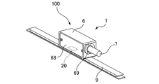
図1に示すように、本形態における磁気センサ装置1は、磁気式リニアエンコーダ装置100(磁気式エンコーダ装置)として構成されている。磁気センサ装置1は、磁気センサ20と、磁気媒体9(磁気スケール)とを有しており、磁気センサ20と磁気媒体9とは対向している。磁気媒体9には、後述するように、長手方向(磁気センサ装置1と磁気媒体9との相対移動方向)に沿ってN極とS極とが交互に配列されたトラックが形成されており、磁気センサ20は、磁気媒体9の表面に形成された回転磁界を検出することにより、磁気センサ20と磁気媒体9とが相対移動した際の移動量や位置を検出する。磁気センサ装置1は、非磁性材料からなるホルダ6と、非磁性材料からなるカバー68と、ホルダ6から延びたケーブル7とを備えており、ホルダ6の内側に磁気センサ20が配置されている。ホルダ6の側面にはケーブル挿通穴69が形成されており、このケーブル挿通穴69からケーブル7が引き出されている。このように構成した磁気センサ装置1においては、磁気センサ20(ホルダ6)および磁気媒体9のうちの一方が固定体側に配置され、他方が移動体側に配置される。本形態では、磁気媒体9が移動体側に配置され、磁気センサ20(ホルダ6)が固定体側に配置される。
As shown in FIG. 1, the
図2(a)、(b)、(c)に示すように、ホルダ6には、磁気媒体9と対向する底面に、段差を介してホルダ6の底面から突出した平坦面からなる基準面60が形成されている。基準面60には開口部65が形成されており、開口部65に対して、シリコン基板やセラミックグレース基板などの素子基板10を備えた磁気センサ20が配置され、センサ
面250が構成されている。素子基板10には、フレキシブル配線基板34が接続されている。
2A, 2B, and 2C, the
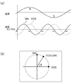
磁気センサ20は、磁気抵抗素子25として、互いに90°の位相差を有するA相の磁気抵抗素子25(A)とB相の磁気抵抗素子25(B)とを有している。なお、図面には、A相の磁気抵抗素子25(A)にはSINを付し、B相の磁気抵抗素子25(B)には、COSを付してある。
The
A相の磁気抵抗素子25(A)は、180°の位相差をもって磁気媒体9の移動検出を行う+a相の磁気抵抗素子25(+a)と−a相の磁気抵抗素子25(−a)とを備えており、図面には、+a相の磁気抵抗素子25(+a)にはSIN+と付し、−a相の磁気抵抗素子25(−a)には、SIN−を付してある。同様に、B相の磁気抵抗素子25(B)は、180°の位相差をもって磁気媒体9の移動検出を行う+b相の磁気抵抗素子25(+b)と−b相の磁気抵抗素子25(−b)とを備えており、図面には、+b相の磁気抵抗素子25(+b)にはCOS+と付し、−b相の磁気抵抗素子25(−b)には、COS−を付してある。
The A-phase magnetoresistive element 25 (A) includes a + a-phase magnetoresistive element 25 (+ a) that detects movement of the
本形態では、+a相の磁気抵抗素子25(+a)、−a相の磁気抵抗素子25(−a)、+b相の磁気抵抗素子25(+b)、および−b相の磁気抵抗素子25(−b)は、1枚の素子基板10の同一の面上(主面上)に形成されている。磁気抵抗素子25(+a)、25(−a)、25(+b)、25(−b)は、素子基板10で格子状に配置されており、+a相の磁気抵抗素子25(+a)と−a相の磁気抵抗素子25(−a)とは対角位置に形成され、+b相の磁気抵抗素子25(+b)と−b相の磁気抵抗素子25(−b)とは対角位置に形成されている。
In this embodiment, a + a phase magnetoresistive element 25 (+ a), a −a phase magnetoresistive element 25 (−a), a + b phase magnetoresistive element 25 (+ b), and a −b phase magnetoresistive element 25 (− b) is formed on the same surface (main surface) of one
磁気媒体9では、移動方向に沿ってN極とS極が交互に並ぶトラック91が形成されており、本形態では、3列のトラック91(91A、91B、91C)が幅方向で並列している。ここで、隣接するトラック91A、91B、91C間では、N極およびS極の位置が移動方向で1磁極分、ずれている。このため、両側のトラック91A、91Cでは、N極およびS極の位置が移動方向で一致している。さらに、隣接するトラック91Aとトラック91Bの境界部分912、およびトラック91Bとトラック91Cの境界部分912は、例えば、磁極が存在しない無着磁部分や非磁性部分を介在させることなく、隣接する当該境界部分912のN極およびS極が直接、接するように形成されている。
In the
このように構成した磁気媒体9において、トラック91A、91B、91Cの境界部分912では、強度の大きな回転磁界が発生している。さらに、本形態では、隣接するトラック91Aとトラック91Bの境界部分912、およびトラック91Bとトラック91Cの境界部分912は、当該境界部分912のN極およびS極が直接、接するように形成されているので、トラック91A、91B、91Cの境界部分912では、より強度の大きな回転磁界が発生している。従って、本形態では、図2(c)に示すように、トラック91A、91B、91Cの境界部分912に対して磁気センサ装置1のセンサ面250を面対向させている。また、センサ面250は、磁気媒体9の幅方向の中央に位置しているため、センサ面250の幅方向における一方の端部251は、3つのトラック91A、91B、91Cのうち、トラック91Aの幅方向の略中央に位置し、他方の端部252は、トラック91Cの幅方向の略中央に位置している。従って、+a相の磁気抵抗素子25(+a)が形成されている領域、および+b相の磁気抵抗素子25(+b)が形成されている領域は、トラック91A、91Bの境界部分912に対向し、−a相の磁気抵抗素子25(−a)が形成されている領域、および−b相の磁気抵抗素子25(−b)が形成されている領域は、トラック91B、91Cの境界部分912に対向している。トラック91Bは、+a
相の磁気抵抗素子25(+a)および+b相の磁気抵抗素子25(+b)が形成されている領域と、−a相の磁気抵抗素子25(−a)および−b相の磁気抵抗素子25(−b)が形成されている領域のそれぞれの領域が対向するトラック、すなわち、兼用する共通のトラック91Bとして磁気媒体9の中央に形成されている。
In the
Phase magnetoresistive element 25 (+ a) and + b phase magnetoresistive element 25 (+ b), -a phase magnetoresistive element 25 (-a) and -b phase magnetoresistive element 25 ( -B) is formed in the center of the
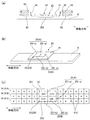
(磁気抵抗素子の構成)
図3は、本発明を適用した磁気式リニアエンコーダ装置100の磁気センサ20に形成した磁気抵抗素子を模式的に示す説明図である。図4は、本発明を適用した磁気式リニアエンコーダ装置100の磁気センサ20に形成した磁気抵抗素子のブリッジ回路の説明図である。図5は、本発明を適用した磁気式リニアエンコーダ装置100における検出原理を示す説明図である。
(Configuration of magnetoresistive element)
FIG. 3 is an explanatory diagram schematically showing a magnetoresistive element formed in the
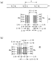
図3に示すように、素子基板10の主面では、素子基板10の長手方向(移動方向)における中央領域に、磁気抵抗素子25(+a)、25(−a)、25(+b)、25(−b)が形成されている。素子基板10の一方側端部11は第1の端子部21とされ、他方側端部12は第2の端子部22とされている。+a相の磁気抵抗素子25(+a)と−a相の磁気抵抗素子25(−a)とは対角位置に形成され、+b相の磁気抵抗素子25(+b)と−b相の磁気抵抗素子25(−b)とは対角位置に形成されている。
As shown in FIG. 3, on the main surface of the
+a相の磁気抵抗素子25(+a)および−a相の磁気抵抗素子25(−a)は、一方端が電源端子212(Vcc)、222(Vcc)に接続され、他方端は、グランド端子213(GND)、223(GND)に接続されている。また、+a相の磁気抵抗素子25(+a)の中点位置には、出力SIN+に対する端子211(+a)が接続し、−a相の磁気抵抗素子25(−a)の中点位置には、出力SIN−に対する端子221(−a)が接続している。従って、図4(a)に示すように、電源端子212(Vcc)、222(Vcc)に電源電位Vccを印加し、グランド端子213(GND)、223(GND)をグランド電位GNDとすれば、出力SIN+および出力SIN−を得ることができる。それ故、出力SIN+および出力SIN−をデジタル化した後、減算器に入力すれば、図5(a)に示すように、磁気媒体9による磁界変化に対応する差動出力SINを得ることができる。
One end of the + a phase magnetoresistive element 25 (+ a) and the −a phase magnetoresistive element 25 (−a) is connected to the power supply terminals 212 (Vcc) and 222 (Vcc), and the other end is connected to the
再び図3において、−b相の磁気抵抗素子25(−b)および−b相の磁気抵抗素子25(+b)は、一方端が電源端子224(Vcc)、214(Vcc)に接続されている。また、+b相の磁気抵抗素子25(+b)の他方端は、+a相の磁気抵抗素子25(+a)と同様、グランド端子213(GND)に接続し、−b相の磁気抵抗素子25(−b)の他方端は、−a相の磁気抵抗素子25(−a)と同様、第2の共通端子としてのグランド端子223(GND)に接続している。さらに、−b相の磁気抵抗素子25(−b)の中点位置には、出力COS−に対する端子225(−b)が接続し、+b相の磁気抵抗素子25(+b)の中点位置には、出力COS+に対する端子215(+b)が接続している。従って、図4(b)に示すように、電源端子224(Vcc)、214(Vcc)に電源電位Vccを印加し、グランド端子213(GND)、223(GND)をグランド電位GNDとすれば、出力COS+および出力COS−を得ることができる。それ故、出力COS+および出力COS−をデジタル化した後、減算器に入力すれば、図5(a)に示すように、磁気媒体9による磁界変化に対応する差動出力COSを得ることができる。
Referring again to FIG. 3, one end of the -b phase magnetoresistive element 25 (-b) and the -b phase magnetoresistive element 25 (+ b) are connected to the power supply terminals 224 (Vcc) and 214 (Vcc). . Similarly to the + a-phase magnetoresistive element 25 (+ a), the other end of the + b-phase magnetoresistive element 25 (+ b) is connected to the ground terminal 213 (GND), and the -b-phase magnetoresistive element 25 (− The other end of b) is connected to a ground terminal 223 (GND) as a second common terminal, similarly to the -a phase magnetoresistive element 25 (-a). Further, a terminal 225 (−b) for the output COS− is connected to the midpoint position of the −b phase magnetoresistive element 25 (−b), and the midpoint position of the + b phase magnetoresistive element 25 (+ b) is connected. Is connected to the terminal 215 (+ b) for the output COS +. Therefore, as shown in FIG. 4B, if the power supply potential Vcc is applied to the power supply terminals 224 (Vcc) and 214 (Vcc) and the ground terminals 213 (GND) and 223 (GND) are set to the ground potential GND, An output COS + and an output COS− can be obtained. Therefore, if the output COS + and the output COS− are digitized and then input to the subtracter, a differential output COS corresponding to the magnetic field change by the
よって、図5(b)に示すように、得られた差動出力SIN、COSを用いて、以下の式
θ=tan-1(SINθ/COSθ)
から逆正接を求めれば、磁気媒体9と磁気センサ20との相対位置を検出することができ
る。
Therefore, as shown in FIG. 5B, using the obtained differential outputs SIN and COS, the following formula θ = tan −1 (SINθ / COSθ)
If the arc tangent is obtained from the above, the relative position between the
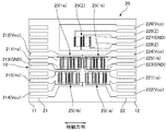
なお、図3に示すように、素子基板10の第1の端子部21には、上記の端子の他にダミーの端子が形成され、第2端子部22にも、上記の端子の他に、ダミーの端子が形成されている。また、素子基板10の長手方向における中央領域には、上記の磁気抵抗素子と隣接する領域に、原点位置を検出するためのZ相の磁気抵抗素子25(Z)が形成され、第2端子部22には、Z相の磁気抵抗素子25(Z)に対する電源端子226(Vcc)、グランド端子227(GND)、出力端子228(Z)、229(Z)も形成されている。
As shown in FIG. 3, dummy terminals are formed in the first
(高調波成分のキャンセル)
図6は、本発明を適用した磁気式リニアエンコーダ装置100の磁気センサ20に形成した高調波キャンセル用の磁気抵抗素子の説明図であり、図6(a)、(b)は、磁極と磁気抵抗素子との関係を示す説明図、および磁気抵抗素子の幅寸法等の説明図である。
(Cancellation of harmonic components)
FIGS. 6A and 6B are explanatory views of a magnetoresistive element for canceling harmonics formed in the
本形態では、磁気センサ20で得られる信号から高調波成分をキャンセルするにあたって、nを整数、mを奇数、kを奇数高調波次数、λを磁極間隔(S極とN極との距離/図6(a)参照)としたとき、磁気センサ20には、磁気媒体9との相対移動方向に沿って、以下の式で求まる距離
(n/2±m/(2×k))λ
上式において、n=整数
m=奇数
k=奇数高調波次数
λ=磁極間隔(S極とN極との間隔)
を隔てた位置に複数の磁気抵抗素子が配置されている。
In this embodiment, when canceling the harmonic component from the signal obtained by the
Where n = integer
m = odd number
k = odd harmonic order
λ = Magnet spacing (distance between S pole and N pole)
A plurality of magnetoresistive elements are arranged at positions separated from each other.
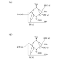
より具体的には、まず、図6(a)に示すように、磁気センサ20では、磁気抵抗素子25(+a)、25(−a)、25(+b)、25(−b)のいずれにおいても、磁気抵抗膜からなる複数の磁気抵抗素子R1〜R4を含む第1磁気抵抗素子群Raと、磁気抵抗膜からなる複数の磁気抵抗素子R11〜R14を含んで第1磁気抵抗素子群Raと対をなす第2磁気抵抗素子群Rbとが設けられている。ここで、磁気抵抗素子R1〜R4、R11〜R14は各々、移動方向と交差する方向(第1方向)に延在し、かつ、移動方向(第2方向)に沿って配列されている。磁気抵抗素子R1〜R4は直列に電気的に接続され、磁気抵抗素子R11〜R14は直列に電気的に接続されている。また、第1磁気抵抗素子群Raと第2磁気抵抗素子群Rbとは直列に電気的に接続されて対をなしている。
More specifically, as shown in FIG. 6A, in the
ここで、複数の磁気抵抗素子R1〜R4、R11〜R14は3次高調波成分および5次高調波成分を打ち消すように配置され、第1磁気抵抗素子群Raと第2磁気抵抗素子群Rbとは7次高調波成分を打ち消すように配置されている。 Here, the plurality of magnetoresistive elements R1 to R4 and R11 to R14 are arranged so as to cancel the third harmonic component and the fifth harmonic component, and the first magnetoresistive element group Ra and the second magnetoresistive element group Rb Are arranged so as to cancel the seventh harmonic component.
より具体的には、第1磁気抵抗素子群Raでは、磁気抵抗素子R1と磁気抵抗素子R2との距離、および磁気抵抗素子R3と磁気抵抗素子R4との距離は、上式において、n=0、m=1、k=5であり、λ/10である。従って、磁気抵抗素子R1と磁気抵抗素子R2との対、および磁気抵抗素子R3と磁気抵抗素子R4との対によって、5次高調波成分をキャンセルすることができる。 More specifically, in the first magnetoresistive element group Ra, the distance between the magnetoresistive element R1 and the magnetoresistive element R2 and the distance between the magnetoresistive element R3 and the magnetoresistive element R4 are n = 0 in the above equation. , M = 1, k = 5, and λ / 10. Therefore, the fifth harmonic component can be canceled by the pair of the magnetoresistive element R1 and the magnetoresistive element R2 and the pair of the magnetoresistive element R3 and the magnetoresistive element R4.
また、第1磁気抵抗素子群Raでは、磁気抵抗素子R1と磁気抵抗素子R3との距離、および磁気抵抗素子R2と磁気抵抗素子R4との距離は、上式において、n=0、m=1、k=3であり、λ/6である。従って、磁気抵抗素子R1と磁気抵抗素子R3との対、および磁気抵抗素子R2と磁気抵抗素子R4との対によって、3次高調波成分をキャンセ
ルすることができる。
In the first magnetoresistive element group Ra, the distance between the magnetoresistive element R1 and the magnetoresistive element R3 and the distance between the magnetoresistive element R2 and the magnetoresistive element R4 are n = 0 and m = 1 in the above equation. , K = 3 and λ / 6. Therefore, the third harmonic component can be canceled by the pair of the magnetoresistive element R1 and the magnetoresistive element R3 and the pair of the magnetoresistive element R2 and the magnetoresistive element R4.
本形態では、上記の基本パターンと同一のパターンをもって、第1磁気抵抗素子群Raと離間する位置に第2磁気抵抗素子群Rbが配置されており、第2磁気抵抗素子群Rbにおいて、磁気抵抗素子R11と磁気抵抗素子R12との距離、および磁気抵抗素子R13と磁気抵抗素子R14との距離は、上式において、n=0、m=1、k=5であり、λ/10である。従って、磁気抵抗素子R11と磁気抵抗素子R12との対、および磁気抵抗素子R13と磁気抵抗素子R14との対によって、5次高調波成分をキャンセルすることができる。 In the present embodiment, the second magnetoresistive element group Rb is arranged at a position separated from the first magnetoresistive element group Ra with the same pattern as the basic pattern described above. The distance between the element R11 and the magnetoresistive element R12 and the distance between the magnetoresistive element R13 and the magnetoresistive element R14 are n = 0, m = 1, k = 5, and λ / 10 in the above equation. Therefore, the fifth harmonic component can be canceled by the pair of the magnetoresistive element R11 and the magnetoresistive element R12 and the pair of the magnetoresistive element R13 and the magnetoresistive element R14.
また、第2磁気抵抗素子群Rbでは、磁気抵抗素子R11と磁気抵抗素子R13との距離、および磁気抵抗素子R12と磁気抵抗素子R14との距離は、上式において、n=0、m=1、k=3であり、λ/6である。従って、磁気抵抗素子R11と磁気抵抗素子R13との対、および磁気抵抗素子R12と磁気抵抗素子R14との対によって、3次高調波成分をキャンセルすることができる。 In the second magnetoresistive element group Rb, the distance between the magnetoresistive element R11 and the magnetoresistive element R13, and the distance between the magnetoresistive element R12 and the magnetoresistive element R14 are n = 0 and m = 1 in the above equation. , K = 3 and λ / 6. Therefore, the third harmonic component can be canceled by the pair of the magnetoresistive element R11 and the magnetoresistive element R13 and the pair of the magnetoresistive element R12 and the magnetoresistive element R14.
ここで、第1磁気抵抗素子群Raと第2磁気抵抗素子群Rbの距離も、上式に基づいて設定されている。本形態において、第1磁気抵抗素子群Raと第2磁気抵抗素子群Rbとの距離は、上式において、n=1、m=1、k=7であり、λ/2+λ/14である。従って、磁気抵抗素子R1と磁気抵抗素子R11との距離は、上式において、n=1、m=1、k=7であり、λ/2+λ/14である。また、磁気抵抗素子R2と磁気抵抗素子R12との距離、磁気抵抗素子R3と磁気抵抗素子R13との距離、および磁気抵抗素子R4と磁気抵抗素子R14との距離も、上式において、n=1、m=1、k=7であり、λ/2+λ/14である。それ故、第1磁気抵抗素子群Raと第2磁気抵抗素子群Rbとによって、7次高調波成分をキャンセルすることができる。 Here, the distance between the first magnetoresistive element group Ra and the second magnetoresistive element group Rb is also set based on the above equation. In this embodiment, the distance between the first magnetoresistive element group Ra and the second magnetoresistive element group Rb is n = 1, m = 1, k = 7 and λ / 2 + λ / 14 in the above equation. Therefore, the distance between the magnetoresistive element R1 and the magnetoresistive element R11 is n = 1, m = 1, k = 7 and λ / 2 + λ / 14 in the above equation. Further, the distance between the magnetoresistive element R2 and R12, the distance between the magnetoresistive element R3 and the magnetoresistive element R13, and the distance between the magnetoresistive element R4 and the magnetoresistive element R14 are n = 1 , M = 1, k = 7, and λ / 2 + λ / 14. Therefore, the seventh harmonic component can be canceled by the first magnetoresistive element group Ra and the second magnetoresistive element group Rb.
(磁気抵抗素子R1〜R4、R11〜R14の間隔の設定例)
図7は、磁気抵抗素子との間における磁界の強さを示す説明図である。
(Setting example of intervals of magnetoresistive elements R1 to R4, R11 to R14)
FIG. 7 is an explanatory diagram showing the strength of the magnetic field between the magnetoresistive element.
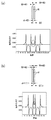
図6(a)を参照して説明したように、磁気抵抗素子R1〜R4、R11〜R14を並列して配置するにあたっては、本形態では、図6(b)に示すように、複数の磁気抵抗素子R1〜R4、R11〜R14のうち、隣り合う磁気抵抗素子との間隔dは、磁気抵抗素子の幅寸法w以上である。かかる構成によれば、以下に説明する理由から、隣り合う磁気抵抗素子同士の磁気的な相互干渉を緩和することができる。 As described with reference to FIG. 6A, when the magnetoresistive elements R1 to R4 and R11 to R14 are arranged in parallel, in this embodiment, as shown in FIG. Among the resistance elements R1 to R4 and R11 to R14, the distance d between adjacent magnetoresistive elements is equal to or greater than the width w of the magnetoresistive elements. According to such a configuration, magnetic mutual interference between adjacent magnetoresistive elements can be mitigated for the reason described below.
例えば、図7(b)に比較例を示すように、磁気抵抗素子Rの幅wを40μmとし、並列する2本の磁気抵抗素子Rの間隔dを40μm未満、例えば、17.1μmとした場合、磁気抵抗素子Rに直交する方向の磁界を印加したときの各位置における磁界の強さをシミュレーションすると、図7(b)において円で囲んで示すように、2本の磁気抵抗素子Rの間でのパーミアンスが大きく、2本の磁気抵抗素子Rの間で磁束密度が高い。従って、図6(a)に示す磁気抵抗素子R1〜R4、R11〜R14において、磁気抵抗素子Rの間隔dが磁気抵抗素子Rの幅寸法wより狭い箇所が存在すると、その両側での出力に差が発生し、高調波成分をキャンセルできなくなってしまう。 For example, as shown in FIG. 7B, when the width w of the magnetoresistive element R is 40 μm and the distance d between the two magnetoresistive elements R in parallel is less than 40 μm, for example, 17.1 μm. When simulating the strength of the magnetic field at each position when a magnetic field in a direction orthogonal to the magnetoresistive element R is applied, as shown in a circle in FIG. 7B, between the two magnetoresistive elements R And the magnetic flux density is high between the two magnetoresistive elements R. Therefore, in the magnetoresistive elements R1 to R4 and R11 to R14 shown in FIG. 6A, if there is a portion where the distance d of the magnetoresistive element R is narrower than the width dimension w of the magnetoresistive element R, the outputs on both sides thereof are output. A difference occurs and harmonic components cannot be canceled.
これに対して、図7(a)に本発明の実施例を示すように、磁気抵抗素子Rの幅寸法wを40μmとし、並列する2本の磁気抵抗素子Rの間隔dを40μm以上、例えば、40μmとした場合、磁気抵抗素子Rに直交する方向の磁界を印加したときの各位置における磁界の強さをシミュレーションすると、2本の磁気抵抗素子Rの間でのパーミアンスが小さく、2本の磁気抵抗素子Rの間で磁束密度が低い。従って、図6(a)に示す磁気抵抗素子R1〜R4、R11〜R14において、磁気抵抗素子Rの間隔dが狭い箇所があって
も、その間隔dが磁気抵抗素子Rの幅寸法w以上であれば、間隔dが狭い箇所の両側でも、出力に差が発生せず、高調波成分をキャンセルすることができる。
On the other hand, as shown in FIG. 7A, the width dimension w of the magnetoresistive element R is set to 40 μm, and the distance d between the two magnetoresistive elements R arranged in parallel is set to 40 μm or more. When the magnetic field strength in each direction when a magnetic field in a direction orthogonal to the magnetoresistive element R is applied is simulated, the permeance between the two magnetoresistive elements R is small and the two magnetoresistive elements R are small. The magnetic flux density is low between the magnetoresistive elements R. Accordingly, in the magnetoresistive elements R1 to R4 and R11 to R14 shown in FIG. 6A, even if there is a portion where the interval d of the magnetoresistive element R is narrow, the interval d is not less than the width dimension w of the magnetoresistive element R. If there is, a difference in output does not occur on both sides of the portion where the distance d is narrow, and the harmonic component can be canceled.
また、磁気抵抗素子R1〜R4、R11〜R14は抵抗値が小さい方が感度が高い。従って、磁気抵抗素子Rの幅寸法wを狭くした場合には、磁気抵抗素子R1〜R4、R11〜R14を構成する磁気抵抗膜の膜厚を大とすることが好ましい。但し、隣り合う磁気抵抗素子同士の磁気的な相互干渉を緩和するという観点から、本形態では、磁気抵抗素子R1〜R4、R11〜R14の膜厚は、磁気抵抗素子Rの幅寸法wより薄い。 Further, the magnetoresistive elements R1 to R4 and R11 to R14 have higher sensitivity when the resistance value is smaller. Accordingly, when the width w of the magnetoresistive element R is narrowed, it is preferable to increase the film thickness of the magnetoresistive films constituting the magnetoresistive elements R1 to R4 and R11 to R14. However, in the present embodiment, the film thicknesses of the magnetoresistive elements R1 to R4 and R11 to R14 are thinner than the width dimension w of the magnetoresistive element R from the viewpoint of reducing the magnetic mutual interference between the adjacent magnetoresistive elements. .
(本形態の主な効果)
以上説明したように、本形態の磁気センサ装置1およびリニアエンコーダ装置100において、磁気センサ20は、磁気媒体9との相対移動方向に沿って複数の磁気抵抗素子R1〜R4、R11〜R14を備えているが、複数の磁気抵抗素子R1〜R4、R11〜R14のうち、隣り合う磁気抵抗素子の間隔dは、磁気抵抗素子の幅寸法w以上である。このため、隣り合う磁気抵抗素子同士の磁気的な相互干渉を緩和することができる。特に本形態において、複数の磁気抵抗素子R1〜R4、R11〜R14は、高調波成分を打ち消すように配置されているため、磁気抵抗素子R1〜R4、R11〜R14同士が近接することになるが、隣り合う磁気抵抗素子の間隔dは、磁気抵抗素子の幅寸法w以上である。このため、隣り合う磁気抵抗素子同士の磁気的な相互干渉を緩和することができるので、高調波成分の影響を効果的に緩和することができる。
(Main effects of this form)
As described above, in the
また、磁気抵抗素子R1〜R4、R11〜R14の膜厚は、磁気抵抗素子Rの幅寸法wより薄い。このため、隣り合う磁気抵抗素子同士の磁気的な相互干渉を緩和することができる。 Further, the film thicknesses of the magnetoresistive elements R1 to R4 and R11 to R14 are thinner than the width dimension w of the magnetoresistive element R. For this reason, the magnetic mutual interference of adjacent magnetoresistive elements can be relieved.
(磁気抵抗素子R1〜R4、R11〜R14の好適例)
図8は、本発明を適用した磁気式リニアエンコーダ装置100の磁気センサ20に形成した磁気抵抗素子のレイアウトの好適例を示す説明図である。
(Preferable examples of magnetoresistive elements R1 to R4, R11 to R14)
FIG. 8 is an explanatory diagram showing a preferred example of the layout of the magnetoresistive elements formed in the
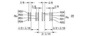
図6等を参照して説明した形態では、5次高調波成分をキャンセルするための磁気抵抗素子R11と磁気抵抗素子R12との距離、および磁気抵抗素子R13と磁気抵抗素子R14との距離がλ/10であったが、本形態では、図8に示すように、5次高調波成分をキャンセルするための磁気抵抗素子の対の距離をλ/2+λ/10に設定し、磁気抵抗素子同士の間隔を広げてある。 In the embodiment described with reference to FIG. 6 and the like, the distance between the magnetoresistive element R11 and the magnetoresistive element R12 for canceling the fifth harmonic component and the distance between the magnetoresistive element R13 and the magnetoresistive element R14 are λ. In this embodiment, as shown in FIG. 8, the distance between the pair of magnetoresistive elements for canceling the fifth harmonic component is set to λ / 2 + λ / 10, and the magnetoresistive elements The interval is widened.
より具体的には、第1磁気抵抗素子群Raでは、磁気抵抗素子R21と磁気抵抗素子R22との距離、および磁気抵抗素子R23と磁気抵抗素子R24との距離は、前記した式において、n=1、m=1、k=5であり、λ/2+λ/10である。従って、磁気抵抗素子R21と磁気抵抗素子R22との対、および磁気抵抗素子R23と磁気抵抗素子R24との対によって、5次高調波成分をキャンセルすることができる。 More specifically, in the first magnetoresistive element group Ra, the distance between the magnetoresistive element R21 and the magnetoresistive element R22 and the distance between the magnetoresistive element R23 and the magnetoresistive element R24 are n = 1, m = 1, k = 5, and λ / 2 + λ / 10. Therefore, the fifth harmonic component can be canceled by the pair of the magnetoresistive element R21 and the magnetoresistive element R22 and the pair of the magnetoresistive element R23 and the magnetoresistive element R24.
また、第1磁気抵抗素子群Raでは、磁気抵抗素子R21と磁気抵抗素子R23との距離、および磁気抵抗素子R22と磁気抵抗素子R24との距離は、前記した式において、n=0、m=1、k=3であり、λ/6である。従って、磁気抵抗素子R21と磁気抵抗素子R23との対、および磁気抵抗素子R22と磁気抵抗素子R24との対によって、3次高調波成分をキャンセルすることができる。 In the first magnetoresistive element group Ra, the distance between the magnetoresistive element R21 and the magnetoresistive element R23, and the distance between the magnetoresistive element R22 and the magnetoresistive element R24 are n = 0 and m = 1, k = 3, and λ / 6. Therefore, the third harmonic component can be canceled by the pair of the magnetoresistive element R21 and the magnetoresistive element R23 and the pair of the magnetoresistive element R22 and the magnetoresistive element R24.
本形態では、上記の基本パターンと同一のパターンをもって、第1磁気抵抗素子群Raと離間する位置に第2磁気抵抗素子群Rbが配置されており、第2磁気抵抗素子群Rbにおいて、磁気抵抗素子R31と磁気抵抗素子R32との距離、および磁気抵抗素子R33
と磁気抵抗素子R34との距離は、前記した式において、n=1、m=1、k=5であり、λ/2+λ/10である。従って、磁気抵抗素子R31と磁気抵抗素子R32との対、および磁気抵抗素子R33と磁気抵抗素子R34との対によって、5次高調波成分をキャンセルすることができる。
In the present embodiment, the second magnetoresistive element group Rb is arranged at a position separated from the first magnetoresistive element group Ra with the same pattern as the basic pattern described above. The distance between the element R31 and the magnetoresistive element R32, and the magnetoresistive element R33
And the magnetoresistive element R34 in the above formula are n = 1, m = 1, k = 5, and λ / 2 + λ / 10. Accordingly, the fifth harmonic component can be canceled by the pair of the magnetoresistive element R31 and the magnetoresistive element R32 and the pair of the magnetoresistive element R33 and the magnetoresistive element R34.
また、第2磁気抵抗素子群Rbでは、磁気抵抗素子R31と磁気抵抗素子R33との距離、および磁気抵抗素子R32と磁気抵抗素子R34との距離は、前記した式において、n=0、m=1、k=3であり、λ/6である。従って、磁気抵抗素子R31と磁気抵抗素子R33との対、および磁気抵抗素子R32と磁気抵抗素子R34との対によって、3次高調波成分をキャンセルすることができる。 In the second magnetoresistive element group Rb, the distance between the magnetoresistive element R31 and the magnetoresistive element R33, and the distance between the magnetoresistive element R32 and the magnetoresistive element R34 are n = 0 and m = 1, k = 3, and λ / 6. Therefore, the third harmonic component can be canceled by the pair of the magnetoresistive element R31 and the magnetoresistive element R33 and the pair of the magnetoresistive element R32 and the magnetoresistive element R34.
ここで、第1磁気抵抗素子群Raと第2磁気抵抗素子群Rbの距離も、前記した式に基づいて設定されている。本形態において、第1磁気抵抗素子群Raと第2磁気抵抗素子群Rbとの距離は、上式において、n=2、m=1、k=7であり、λ+λ/14である。従って、磁気抵抗素子R21と磁気抵抗素子R31との距離は、上式において、n=2、m=1、k=7であり、λ+λ/14である。また、磁気抵抗素子R22と磁気抵抗素子R32との距離、磁気抵抗素子R23と磁気抵抗素子R33との距離、および磁気抵抗素子R24と磁気抵抗素子R34との距離も、上式において、n=2、m=1、k=7であり、λ+λ/14である。それ故、第1磁気抵抗素子群Raと第2磁気抵抗素子群Rbとによって、7次高調波成分をキャンセルすることができる。 Here, the distance between the first magnetoresistive element group Ra and the second magnetoresistive element group Rb is also set based on the above equation. In this embodiment, the distance between the first magnetoresistive element group Ra and the second magnetoresistive element group Rb is n = 2, m = 1, k = 7 and λ + λ / 14 in the above equation. Accordingly, the distance between the magnetoresistive element R21 and the magnetoresistive element R31 is n = 2, m = 1, k = 7, and λ + λ / 14 in the above equation. Also, the distance between the magnetoresistive element R22 and the magnetoresistive element R32, the distance between the magnetoresistive element R23 and the magnetoresistive element R33, and the distance between the magnetoresistive element R24 and the magnetoresistive element R34 are n = 2 in the above equation. , M = 1, k = 7, and λ + λ / 14. Therefore, the seventh harmonic component can be canceled by the first magnetoresistive element group Ra and the second magnetoresistive element group Rb.
このような構成であれば、5次高調波成分を打ち消すための磁気抵抗素子の対(磁気抵抗素子R21と磁気抵抗素子R22との対、磁気抵抗素子R23と磁気抵抗素子R24との対、磁気抵抗素子R31と磁気抵抗素子R32との対、および磁気抵抗素子R33と磁気抵抗素子R34との対)でも、十分な距離を隔てた位置に配置される。従って、磁気抵抗素子R21〜R24、R31〜R34では、最も間隔が狭い箇所でもλ/6の間隔がある。それ故、隣り合う磁気抵抗素子の間隔dを、磁気抵抗素子の幅寸法w以上にするのが容易である。 With such a configuration, a pair of magnetoresistive elements (a pair of magnetoresistive element R21 and magnetoresistive element R22, a pair of magnetoresistive element R23 and magnetoresistive element R24, and a magnetic field for canceling the fifth harmonic component) The pair of the resistor element R31 and the magnetoresistive element R32, and the pair of the magnetoresistive element R33 and the magnetoresistive element R34) are also arranged at a sufficient distance. Therefore, in the magnetoresistive elements R21 to R24 and R31 to R34, there is a λ / 6 interval even at the narrowest interval. Therefore, it is easy to make the distance d between adjacent magnetoresistive elements equal to or greater than the width dimension w of the magnetoresistive elements.
[その他の磁気式エンコーダ装置の構成]
上記形態はいずれも、磁気センサ装置をリニアエンコーダ装置として構成した例であったが、磁気センサ20と磁気媒体9とが、S極とN極とが配列している方向に沿って相対的に回転移動するロータリエンコーダ装置を構成してもよい。
[Configuration of other magnetic encoder devices]
Each of the above forms is an example in which the magnetic sensor device is configured as a linear encoder device. However, the
1・・磁気センサ装置
9・・磁気媒体
20・・磁気センサ
25・・磁気抵抗素子
25(+a)・・+a相の磁気抵抗素子
25(−a)・・−a相の磁気抵抗素子
25(+b)・・+b相の磁気抵抗素子
25(−b)・・−b相の磁気抵抗素子
Ra・・第1磁気抵抗素子群
Rb・・第2磁気抵抗素子群
R1〜R4、R11〜R14、R21〜R24、R31〜R34・・磁気抵抗素子
1.
Claims (10)
前記磁気媒体に対向し、前記磁気媒体との相対移動に伴う磁界変化を検出する磁気センサと、
を有し、
前記磁気媒体は、前記磁気センサとの相対移動方向に沿ってS極とN極とが交互に配置された磁気センサ装置であって、
前記磁気センサは、前記相対移動方向に沿って複数の磁気抵抗素子を備え、
前記複数の磁気抵抗素子のうち、隣り合う磁気抵抗素子の間隔は、前記磁気抵抗素子の幅寸法以上であることを特徴とする磁気センサ装置。 Magnetic media;
A magnetic sensor that faces the magnetic medium and detects a magnetic field change accompanying a relative movement with the magnetic medium;
Have
The magnetic medium is a magnetic sensor device in which S poles and N poles are alternately arranged along a relative movement direction with respect to the magnetic sensor,
The magnetic sensor includes a plurality of magnetoresistive elements along the relative movement direction,
Among the plurality of magnetoresistive elements, an interval between adjacent magnetoresistive elements is equal to or greater than a width dimension of the magnetoresistive elements.
(n/2±m/(2×k))λ
上式において、n=整数
m=奇数
k=奇数高調波次数
λ=磁極間隔(S極とN極との間隔)
を隔てていることを特徴とする請求項3に記載の磁気センサ装置。 The magnetoresistive element has a distance (n / 2 ± m / (2 × k)) λ
Where n = integer
m = odd number
k = odd harmonic order
λ = Magnet spacing (distance between S pole and N pole)
The magnetic sensor device according to claim 3, wherein the magnetic sensor device is separated.
λ/6の間隔を隔てた磁気抵抗素子の対と、
λ/2+λ/10の間隔を隔てた磁気抵抗素子の対と、
が含まれていることを特徴とする請求項4に記載の磁気センサ装置。 In the plurality of magnetoresistive elements,
a pair of magnetoresistive elements spaced apart by λ / 6;
a pair of magnetoresistive elements spaced apart by λ / 2 + λ / 10;
The magnetic sensor device according to claim 4, further comprising:
前記磁気センサと前記磁気媒体とは、S極とN極とが配列している方向に沿って相対的に直線移動することを特徴とする磁気式エンコーダ装置。 A magnetic encoder device comprising the magnetic sensor device according to any one of claims 1 to 6,
The magnetic encoder device, wherein the magnetic sensor and the magnetic medium move relatively linearly along a direction in which an S pole and an N pole are arranged.
前記センサと前記磁気媒体とは、S極とN極とが配列している方向に沿って相対的に回転移動することを特徴とする磁気式エンコーダ装置。 A magnetic encoder device comprising the magnetic sensor device according to any one of claims 1 to 6,
The magnetic encoder device, wherein the sensor and the magnetic medium are relatively rotated and moved along a direction in which an S pole and an N pole are arranged.
前記複数の磁気抵抗素子のうち、隣り合う磁気抵抗素子の間隔は、前記磁気抵抗素子の幅寸法以上であることを特徴とする磁気センサ。 A plurality of magnetoresistive elements extending in the first direction are arranged in a second direction intersecting the first direction,
Among the plurality of magnetoresistive elements, an interval between adjacent magnetoresistive elements is equal to or greater than a width dimension of the magnetoresistive elements.
に記載の磁気センサ。
The thickness of the magnetoresistive element is thinner than the width of the magnetoresistive element.
The magnetic sensor described in 1.
Priority Applications (4)
| Application Number | Priority Date | Filing Date | Title |
|---|---|---|---|
| JP2013254625A JP2015114138A (en) | 2013-12-10 | 2013-12-10 | Magnetic sensor device, magnetic encoder device, and magnetic sensor |
| PCT/JP2014/081678 WO2015087726A1 (en) | 2013-12-10 | 2014-12-01 | Magnetic sensor device, magnetic encoder device, and magnetic sensor |
| CN201410717574.0A CN104697555A (en) | 2013-12-10 | 2014-12-01 | Magnetic sensor device, magnetic encoder device, and magnetic sensor |
| CN201420742962.XU CN204241009U (en) | 2013-12-10 | 2014-12-01 | Magnet sensor arrangement, magnetic encoder apparatus and Magnetic Sensor |
Applications Claiming Priority (1)
| Application Number | Priority Date | Filing Date | Title |
|---|---|---|---|
| JP2013254625A JP2015114138A (en) | 2013-12-10 | 2013-12-10 | Magnetic sensor device, magnetic encoder device, and magnetic sensor |
Publications (1)
| Publication Number | Publication Date |
|---|---|
| JP2015114138A true JP2015114138A (en) | 2015-06-22 |
Family
ID=52770492
Family Applications (1)
| Application Number | Title | Priority Date | Filing Date |
|---|---|---|---|
| JP2013254625A Pending JP2015114138A (en) | 2013-12-10 | 2013-12-10 | Magnetic sensor device, magnetic encoder device, and magnetic sensor |
Country Status (3)
| Country | Link |
|---|---|
| JP (1) | JP2015114138A (en) |
| CN (2) | CN204241009U (en) |
| WO (1) | WO2015087726A1 (en) |
Cited By (1)
| Publication number | Priority date | Publication date | Assignee | Title |
|---|---|---|---|---|
| JP2018132359A (en) * | 2017-02-14 | 2018-08-23 | 日本電産サンキョー株式会社 | Rotary encoder |
Families Citing this family (6)
| Publication number | Priority date | Publication date | Assignee | Title |
|---|---|---|---|---|
| JP2015114138A (en) * | 2013-12-10 | 2015-06-22 | 日本電産サンキョー株式会社 | Magnetic sensor device, magnetic encoder device, and magnetic sensor |
| US9733317B2 (en) | 2014-03-10 | 2017-08-15 | Dmg Mori Seiki Co., Ltd. | Position detecting device |
| JP7064966B2 (en) * | 2018-06-05 | 2022-05-11 | 日本電産サンキョー株式会社 | Magnetic encoder |
| JP6973421B2 (en) * | 2019-01-14 | 2021-11-24 | 株式会社デンソー | Rotation detector |
| DE102021125964A1 (en) * | 2021-10-06 | 2023-04-06 | Infineon Technologies Ag | A position sensor system, an optical lens system and a display |
| JP7452562B2 (en) * | 2022-03-01 | 2024-03-19 | Tdk株式会社 | Magnetic sensor, magnetic encoder, lens position detection device, distance measuring device, and method for manufacturing magnetic sensor |
Family Cites Families (12)
| Publication number | Priority date | Publication date | Assignee | Title |
|---|---|---|---|---|
| JPS62204118A (en) * | 1986-03-05 | 1987-09-08 | Hitachi Ltd | A device that magnetically detects position or speed |
| JP2529960B2 (en) * | 1987-03-14 | 1996-09-04 | 株式会社日立製作所 | Magnetic position detector |
| JPH01116408A (en) * | 1987-10-30 | 1989-05-09 | Yaskawa Electric Mfg Co Ltd | magnetic encoder |
| JPH0618279A (en) * | 1992-06-30 | 1994-01-25 | Hitachi Ltd | Position detector |
| DE4319322C2 (en) * | 1993-06-11 | 1998-04-23 | Heidenhain Gmbh Dr Johannes | Position measuring device |
| JPH09218053A (en) * | 1996-02-08 | 1997-08-19 | Sankyo Seiki Mfg Co Ltd | Magnetic type encoder |
| CN100501835C (en) * | 2005-09-30 | 2009-06-17 | 日立金属株式会社 | Magnetic encoder |
| CN101936749A (en) * | 2006-03-06 | 2011-01-05 | 日本电产三协株式会社 | Magnetic encoder device |
| JP4524758B2 (en) * | 2006-04-14 | 2010-08-18 | 日立金属株式会社 | Magnetic encoder |
| JP4232808B2 (en) * | 2006-09-19 | 2009-03-04 | 日立金属株式会社 | Magnetic encoder device |
| TWI393867B (en) * | 2007-04-20 | 2013-04-21 | Mitsubishi Electric Corp | Magnetic rotation angle detector |
| JP2015114138A (en) * | 2013-12-10 | 2015-06-22 | 日本電産サンキョー株式会社 | Magnetic sensor device, magnetic encoder device, and magnetic sensor |
-
2013
- 2013-12-10 JP JP2013254625A patent/JP2015114138A/en active Pending
-
2014
- 2014-12-01 CN CN201420742962.XU patent/CN204241009U/en not_active Expired - Fee Related
- 2014-12-01 CN CN201410717574.0A patent/CN104697555A/en active Pending
- 2014-12-01 WO PCT/JP2014/081678 patent/WO2015087726A1/en not_active Ceased
Cited By (1)
| Publication number | Priority date | Publication date | Assignee | Title |
|---|---|---|---|---|
| JP2018132359A (en) * | 2017-02-14 | 2018-08-23 | 日本電産サンキョー株式会社 | Rotary encoder |
Also Published As
| Publication number | Publication date |
|---|---|
| CN104697555A (en) | 2015-06-10 |
| CN204241009U (en) | 2015-04-01 |
| WO2015087726A1 (en) | 2015-06-18 |
Similar Documents
| Publication | Publication Date | Title |
|---|---|---|
| JP2015114138A (en) | Magnetic sensor device, magnetic encoder device, and magnetic sensor | |
| JP5064492B2 (en) | Magnetic rotation angle detector | |
| JP6474721B2 (en) | Magnetic sensor device and magnetic encoder device | |
| CN105785290B (en) | Magnetic field sensor | |
| JP6969581B2 (en) | Rotation angle detector | |
| JP6472175B2 (en) | Position detection device | |
| WO2007102465A1 (en) | Magnetic sensor device, magnetic encoder device, and magnetic scale manufacturing method | |
| JP6928782B2 (en) | Magnetic position detector | |
| JP4999498B2 (en) | Magnetic encoder device | |
| JP2016223894A (en) | Magnetic sensor | |
| CN103221790B (en) | Rotation angle detection apparatus | |
| JPWO2017073280A1 (en) | Magnetic detection device and moving body detection device | |
| JP2016050841A (en) | Magnetism detection device | |
| JP2009025047A (en) | Magnetic sensor and magnetic encoder provided with the same | |
| WO2017094828A1 (en) | Position detection device | |
| JP5989257B2 (en) | Magnetic detector | |
| JP7156249B2 (en) | Position detector | |
| JP6455314B2 (en) | Rotation detector | |
| JP4487093B2 (en) | Magnetic sensor | |
| JP2013234939A (en) | Magnetic detection device and magnetic encoder | |
| JPWO2009051069A1 (en) | GMR sensor | |
| JP7463593B2 (en) | Magnetic sensor system and lens position detection device | |
| JP2005069744A (en) | Magnetic detection element | |
| TWI714107B (en) | Electric current sensor | |
| JP5013135B2 (en) | Magnetic position detector |