JP2015099146A - Coverage enhancement and power aware clock system for structural delay-fault test - Google Patents
Coverage enhancement and power aware clock system for structural delay-fault test Download PDFInfo
- Publication number
- JP2015099146A JP2015099146A JP2014228018A JP2014228018A JP2015099146A JP 2015099146 A JP2015099146 A JP 2015099146A JP 2014228018 A JP2014228018 A JP 2014228018A JP 2014228018 A JP2014228018 A JP 2014228018A JP 2015099146 A JP2015099146 A JP 2015099146A
- Authority
- JP
- Japan
- Prior art keywords
- clock
- test
- scan
- clock gating
- clock signal
- Prior art date
- Legal status (The legal status is an assumption and is not a legal conclusion. Google has not performed a legal analysis and makes no representation as to the accuracy of the status listed.)
- Pending
Links
Images


Classifications
-
- G—PHYSICS
- G01—MEASURING; TESTING
- G01R—MEASURING ELECTRIC VARIABLES; MEASURING MAGNETIC VARIABLES
- G01R31/00—Arrangements for testing electric properties; Arrangements for locating electric faults; Arrangements for electrical testing characterised by what is being tested not provided for elsewhere
- G01R31/28—Testing of electronic circuits, e.g. by signal tracer
- G01R31/317—Testing of digital circuits
- G01R31/3181—Functional testing
- G01R31/3185—Reconfiguring for testing, e.g. LSSD, partitioning
- G01R31/318533—Reconfiguring for testing, e.g. LSSD, partitioning using scanning techniques, e.g. LSSD, Boundary Scan, JTAG
- G01R31/318575—Power distribution; Power saving
-
- G—PHYSICS
- G01—MEASURING; TESTING
- G01R—MEASURING ELECTRIC VARIABLES; MEASURING MAGNETIC VARIABLES
- G01R31/00—Arrangements for testing electric properties; Arrangements for locating electric faults; Arrangements for electrical testing characterised by what is being tested not provided for elsewhere
- G01R31/12—Testing dielectric strength or breakdown voltage ; Testing or monitoring effectiveness or level of insulation, e.g. of a cable or of an apparatus, for example using partial discharge measurements; Electrostatic testing
- G01R31/14—Circuits therefor, e.g. for generating test voltages, sensing circuits
-
- G—PHYSICS
- G01—MEASURING; TESTING
- G01R—MEASURING ELECTRIC VARIABLES; MEASURING MAGNETIC VARIABLES
- G01R31/00—Arrangements for testing electric properties; Arrangements for locating electric faults; Arrangements for electrical testing characterised by what is being tested not provided for elsewhere
- G01R31/28—Testing of electronic circuits, e.g. by signal tracer
- G01R31/317—Testing of digital circuits
- G01R31/3181—Functional testing
- G01R31/3185—Reconfiguring for testing, e.g. LSSD, partitioning
- G01R31/318533—Reconfiguring for testing, e.g. LSSD, partitioning using scanning techniques, e.g. LSSD, Boundary Scan, JTAG
- G01R31/318541—Scan latches or cell details
-
- G—PHYSICS
- G01—MEASURING; TESTING
- G01R—MEASURING ELECTRIC VARIABLES; MEASURING MAGNETIC VARIABLES
- G01R31/00—Arrangements for testing electric properties; Arrangements for locating electric faults; Arrangements for electrical testing characterised by what is being tested not provided for elsewhere
- G01R31/28—Testing of electronic circuits, e.g. by signal tracer
- G01R31/317—Testing of digital circuits
- G01R31/3181—Functional testing
- G01R31/3185—Reconfiguring for testing, e.g. LSSD, partitioning
- G01R31/318533—Reconfiguring for testing, e.g. LSSD, partitioning using scanning techniques, e.g. LSSD, Boundary Scan, JTAG
- G01R31/318552—Clock circuits details
Landscapes
- Engineering & Computer Science (AREA)
- Physics & Mathematics (AREA)
- General Physics & Mathematics (AREA)
- General Engineering & Computer Science (AREA)
- Power Engineering (AREA)
- Semiconductor Integrated Circuits (AREA)
- Tests Of Electronic Circuits (AREA)
Abstract
Description
本開示は、例えば遅延故障構造テストの間に使用される、スキャン回路、クロックゲーティングセル、および、スキャン回路のクロックシステムに適用される方法に関する。より具体的には、いくつかの実施形態は、部分的に制御可能なまたは制御不可能な論理がスキャン回路に存在する場合でも、クロック信号を制御可能な状態に維持することに関する。さらなる実施形態は、テストフェーズの間の電力消費量を低減することに関する。 The present disclosure relates to a scan circuit, a clock gating cell, and a method applied to a clock system of the scan circuit, for example, used during a delay fault structure test. More specifically, some embodiments relate to maintaining the clock signal in a controllable state even when partially controllable or uncontrollable logic is present in the scan circuit. Further embodiments relate to reducing power consumption during the test phase.
ここ10年間にわたる集積回路(IC;チップ、マイクロチップ、電子回路など)の開発における著しい進歩は、サブミクロンまで、ましてや、ナノメートルレジームまでさえも、設計構造の関連スケールを縮小させた。以下、「集積回路」は、例えば、論理ゲート、フリップフロップ、マルチプレクサおよび他の回路を含むデジタル電子回路のセットを含むデジタル集積回路に関連する。そのような小型の構造は、一方では、総合設計の複雑性の増加と併せて、他方では、半導体企業にとって、彼らのチップにおける欠陥を低減するという課題を非常に困難なものにする。集積回路の開発コストを削減するため、企業は、彼らの製品をスキャンテストの対象とする。構造が小さくなるほど、高いテスト網羅率を得るのがより難しくなり、高いテスト網羅率は、より高い品質の製品を含意する。サブミクロンおよびナノメートル構造は、機能上の欠陥(例えば、デバイスの相互接続における短絡または開放)に悩まされるばかりでなく、特に、タイミング関連の遅延欠陥(高インピーダンス短絡、インライン抵抗、信号間のクロストークなど)にも悩まされる。前者は、静的テスト(例えば、縮退故障モデルおよびIDDQ故障モデル)で効果的に検出することができるが、後者は、実動作速度テスト(at−speed test)を通じてのみアクセスすることができる。利用可能な自動テストパターン生成(ATPG)ツールは、遅延欠陥に対処することができる。通常、実動作速度故障モデル(例えば、頻繁に使用される実動作速度テストのいくつかを挙げると、ラウンチオフシフト(launch−off−shift)またはスキュードロード(skewed−load)方法を使用する遷移遅延故障モデル、ラウンチオフキャプチャ(launch−off−capture)またはブロードサイド(broadside)方法を使用する遷移遅延故障モデル、パス遅延故障モデル)は、2つの部分からなる。第1の部分の間、検証すべき論理遷移に着手し、第2の部分では、1アプリケーション期間後に応答がキャプチャされ(以下、「キャプチャサイクル」と呼ぶ)、アプリケーション期間は、例えば、クロック周期と同一である。 Significant advances in the development of integrated circuits (ICs; chips, microchips, electronic circuits, etc.) over the last decade have reduced the relevant scale of design structures down to the submicron and even to the nanometer regime. Hereinafter, “integrated circuit” refers to a digital integrated circuit including a set of digital electronic circuits including, for example, logic gates, flip-flops, multiplexers, and other circuits. Such a compact structure, on the one hand, increases the complexity of the overall design, and on the other hand, makes the task of reducing defects in their chips very difficult for semiconductor companies. To reduce the cost of developing integrated circuits, companies target their products for scan testing. The smaller the structure, the more difficult it is to obtain a high test coverage, which implies a higher quality product. Submicron and nanometer structures not only suffer from functional defects (eg, shorts or opens in device interconnects), but especially timing related delay defects (high impedance shorts, in-line resistance, cross between signals) Talk etc.) The former can be effectively detected with static tests (eg, stuck-at fault model and IDDQ fault model), while the latter can only be accessed through an at-speed test. Available automatic test pattern generation (ATPG) tools can address delay defects. Typically, real speed fault models (e.g., transitions using launch-off-shift or skewed-load methods to name some of the frequently used real speed tests) The delay fault model, the transition delay fault model using the launch-off-capture or broadside method, the path delay fault model) has two parts. During the first part, the logic transition to be verified is undertaken, and in the second part, the response is captured after one application period (hereinafter referred to as “capture cycle”). Are the same.
前述のテストモデルのいずれも、集積回路のテスト回路が制御不可能なまたは部分的に制御可能な論理を含む時点で、効果がなくなり、結果的に、低いテスト網羅率をもたらすようになる。多くのチップ製造業者は、彼らのチップ設計に、例えば、いわゆる知的財産(IP)モジュールを組み込み、その挙動は、テスト動作の間ではなく、機能上の動作の間でのみよく知られている。そのような制御不可能なまたは部分的に制御可能な論理は、テスト動作の間の制御不可能なまたは部分的に制御可能な出力信号の原因となり得、アクセス可能なテストベクトルの数への強い制約を押し付け、低いテスト網羅率をもたらす。実動作速度遅延故障構造テストに関連する以前の技術分野では、そのような問題には未だ対処していない。 Any of the aforementioned test models are ineffective when the integrated circuit test circuitry includes uncontrollable or partially controllable logic, resulting in low test coverage. Many chip manufacturers incorporate, for example, so-called intellectual property (IP) modules in their chip designs, whose behavior is only known during functional operations, not during test operations . Such uncontrollable or partially controllable logic can cause uncontrollable or partially controllable output signals during the test operation and is strong on the number of accessible test vectors Impose constraints and result in low test coverage. Previous technical fields related to real speed delay fault structure testing have not yet addressed such issues.
本開示の目的は、とりわけ、制御不可能なまたは部分的に制御可能な論理によって遅延故障テストのクロックシステム内で発生する問題の回避によるテスト網羅率の向上を対象とするものであり得る。 The purpose of the present disclosure may be directed, inter alia, to improving test coverage by avoiding problems that occur in a clock system for delay fault testing due to uncontrollable or partially controllable logic.
1つまたは複数のクロックゲーティングセルを含むスキャンテストのスキャン回路のクロックシステムに適用される方法が提供される。方法は、スキャンテストのいかなる段階でも、各クロックゲーティングセルでクロック信号の制御可能な波形を出力するステップと、キャプチャサイクルの間に、各クロックゲーティングセルで部分的イネーブルクロック信号を除去するステップとを含む。 A method applied to a clock system of a scan circuit for a scan test including one or more clock gating cells is provided. The method includes outputting a controllable waveform of the clock signal at each clock gating cell at any stage of the scan test and removing a partial enable clock signal at each clock gating cell during a capture cycle. Including.
さらに、クロックゲーティングセルが提供される。クロックゲーティングセルは、遅延故障スキャン構造テストのキャプチャサイクルの間に、クロック信号の制御可能な波形を出力し、テストのキャプチャサイクルの間に、部分的イネーブルクロック信号を除去するように適合される。 In addition, a clock gating cell is provided. The clock gating cell is adapted to output a controllable waveform of the clock signal during the delay fault scan structure test capture cycle and to remove the partially enabled clock signal during the test capture cycle. .
添付の図面は、本開示のさらなる理解を提供するために含まれ、この明細書に組み込まれ、この明細書の一部を構成する。図面は、本開示の実施形態を示し、記述と共に、本開示の原理の説明に役立つ。本開示の他の実施形態および本開示の意図する利点の多くは、以下の発明を実施するための形態を参照することによってより良く理解されるようになるため、容易に理解されよう。 The accompanying drawings are included to provide a further understanding of the disclosure, and are incorporated in and constitute a part of this specification. The drawings illustrate embodiments of the disclosure and, together with the description, serve to explain the principles of the disclosure. Many of the other embodiments of the present disclosure and the intended advantages of the present disclosure will be readily understood as they become better understood by reference to the following detailed description.
スキャン回路における実動作速度遅延故障構造テストの低い網羅率は周知の問題である。多くの集積回路は、例えば、いわゆる知的財産(IP)モジュール、非スキャンフリップフロップ、内蔵メモリおよび「ブラックボックス」のような制御不可能なまたは部分的に制御可能な論理を含み、その挙動は、個々の機能上の実装形態に依存する。それらの制御不可能なまたは部分的に制御可能な論理は、機能上の(非テスト)動作の間に周知の挙動を呈するが、スキャンテストの間のそれらの挙動は、一般に、前もってアクセスすることはできない。これは、機能上の動作の間にアクセス可能なものより大きなパラメータスペースを網羅する、スキャンテストの間の大多数のテストベクトルが原因である。それは、テスト網羅率を劇的に低減する、スキャン回路における何らかの論理のこの制御不可能なまたは部分的に制御可能な挙動である。 The low coverage of the actual operating speed delay fault structure test in the scan circuit is a well-known problem. Many integrated circuits include uncontrollable or partially controllable logic such as, for example, so-called intellectual property (IP) modules, non-scan flip-flops, built-in memory and “black boxes” whose behavior is , Depends on the implementation on individual functions. Their uncontrollable or partially controllable logic exhibits well-known behavior during functional (non-test) operations, but their behavior during scan testing is generally accessible in advance I can't. This is due to the majority of test vectors during the scan test that cover a larger parameter space than is accessible during functional operation. It is this uncontrollable or partially controllable behavior of some logic in the scan circuit that dramatically reduces test coverage.
実動作速度遅延故障構造テスト(完全なリストを提供せずに、2つの最も重要なものを挙げると、遷移遅延故障テスト、パス遅延故障テスト)の間、テストのキャプチャサイクルの間に、例えば、部分的に制御可能なまたは制御不可能な論理回路に接続され得る各クロックゲーティングセルの出力で、歪みのないクロック信号を維持することが重要である。部分的に制御可能なまたは制御不可能な論理の出力での部分的に制御可能なまたは制御不可能な信号は、クロックゲーティングセルの入力でのクロック信号の部分的イネーブル信号を引き起こす可能性がある。クロックゲーティングセルの出力で恐らく結果として得られる歪みクロック信号は、以降、「部分的イネーブルクロック信号」で示される(以下では、用語「信号」が使用され、網羅的ではなく、周波数、パルスなどや、当業者によく知られている他の表現を含み得る)。制御可能なクロック信号を維持しなければ、自動テストパターン生成(ATPG)ツールは、クロックゲーティングセルの出力でのクロック信号を定義することはできない。これが、不正確なテストおよび結果的に低いテスト網羅率をもたらす理由の1つである。他方では、スキャンテストの間、テストされている経路に関係なく、多くのフリップフロップが切り替わる可能性がある。これは、スキャンテストの間の電力消費量の上昇を引き起こす。問題については図1で要約され、この図は、2つのクロックドメインを含むシステムオンチップ(SoC)1に関連する。fast_clk_oは、クロックゲーティングセル2a、2b、2c、2dのクロックパス(CP)入力で終端する高速またはマスタクロックを示す。クロック信号は、クロック制御ユニット3によって提供される。fast_clk_en_oおよびslow_clk_en_oはそれぞれ、入力ENでクロックゲーティングセル2a、2b、2c、2dを制御する高速および低速クロックイネーブル(EN)信号である。クロックゲーティングセル(CG)は、網羅的ではなく、1つまたはいくつかのフリップフロップ、1つまたはいくつかのマルチプレクサ、1つまたはいくつかの論理ゲートから構成され得る。クロックゲーティングセルの出力(CPEN)の可能な形態は、事例1、3、5および7として示されている。スキャンテストの実動作速度キャプチャサイクルの間は、事例1および事例5の波形のみが望ましい。事例3−1は、部分的イネーブルクロック信号の一例を表示し、高速クロックが低速クロックに切り替わり、高速ドメインに現れた故障が低速ドメインでテストされる(不正確なテスト網羅率をもたらす)事例である。事例3−2および3−3では、部分的イネーブルクロック信号のより多くの例が示されている。クロックパルスが欠けており、それにより、ATPGツールの非効率性をもたらすが、その理由は、後者がクロック信号を定義できないためであり、したがって、低いテスト網羅率をもたらす。事例7−1の部分的イネーブルクロック信号は、低速クロックが高速クロックに切り替わることに相当し、すなわち、低速ドメインに現れた故障が高速ドメインでテストされる(不正確なテスト網羅率をもたらす)。事例7−2および7−3は、クロックパルスが欠けた部分的イネーブルクロック信号を表示し、事例3−2および3−3に類似して、ATPGツールの非効率性をもたらし、したがって、低いテスト網羅率をもたらす。望ましくない波形3−1、3−2、3−3および7−1、7−2、7−3は、機能的制御5bおよび5dからそれぞれ生じ、それは、機能上の(非テスト)動作の間でのみ制御可能であるが、スキャンテストの間は制御不可能であり得る。
During the actual operating speed delay fault structure test (without providing a complete list, the two most important ones are transition delay fault test, path delay fault test), during the test capture cycle, for example, It is important to maintain an undistorted clock signal at the output of each clock gating cell that can be connected to a partially controllable or uncontrollable logic circuit. A partially controllable or uncontrollable signal at the output of a partially controllable or uncontrollable logic can cause a partial enable signal for the clock signal at the input of the clock gating cell. is there. The resulting distorted clock signal, possibly resulting from the output of the clock gating cell, will be referred to hereinafter as a “partial enable clock signal” (the term “signal” is used below and is not exhaustive, such as frequency, pulse, etc. And other expressions well known to those skilled in the art). Without maintaining a controllable clock signal, an automatic test pattern generation (ATPG) tool cannot define a clock signal at the output of the clock gating cell. This is one reason for inaccurate testing and consequently low test coverage. On the other hand, during a scan test, many flip-flops can switch regardless of the path being tested. This causes an increase in power consumption during the scan test. The problem is summarized in FIG. 1, which relates to a system on chip (SoC) 1 that includes two clock domains. fast_clk_o indicates a high-speed or master clock that terminates at the clock path (CP) input of the
図1はスキャンテストの間のすべての可能なクロック信号関連問題の限られた簡易化された選択のみを示すことが含意される。しかし、当業者であれば、同じ課題に関連するはるかに多くの関与問題にそれらを一般化することができよう。 FIG. 1 is implied to show only a limited simplified selection of all possible clock signal related issues during scan testing. However, one of ordinary skill in the art will be able to generalize them to a much larger number of engagement issues related to the same task.
本開示の実施形態による方法は、個々のクロックゲーティングセルCGの出力CPENでの望ましくない波形(例えば、それらのいくつかは、図1で描写される事例3−1、3−2、3−3、7−1、7−2、7−3の部分的イネーブルクロック信号)の除去を対象とし、ATPGツールによる1つまたは複数の制御可能なクロック信号の定義を可能にする。望ましくない波形は、例えば、制御不可能なまたは部分的に制御可能な論理回路5b、5dが原因で、クロックゲーティングセルの1つの入力(EN)での部分的イネーブル信号4b、4dによって生じる可能性がある。この方法は、クロックゲーティングセルの各々の電力消費量制御によって修正することができる。
The method according to an embodiment of the present disclosure may include an undesirable waveform at the output CPEN of an individual clock gating cell CG (eg, some of them are illustrated in cases 3-1, 3-2, 3-, depicted in FIG. 3, 7-1, 7-2, 7-3 partial enable clock signals), allowing the ATPG tool to define one or more controllable clock signals. Undesirable waveforms can be caused by partial enable
クロックゲーティングセルの設計に対する本方法の影響については、高速/マスタまたは低速/分割クロックレジームでの動作に対してそれぞれ、図2および図3に示されている。出力信号CG_1.clk_oおよびCG_2.clk_oは、図4および図5でそれぞれ参照される実施形態に対して例示的に示されているが、明らかにそれらの実施形態に限定されることはなく、一般的な例として機能する。両方の図では、CCU.fast_clk_oは、アプリケーションクロックを示し、これに限定されないが、システムクロック信号であり得る。 The impact of this method on the design of the clock gating cell is illustrated in FIGS. 2 and 3 for operation in the high speed / master or low speed / divided clock regime, respectively. Output signal CG_1. clk_o and CG_2. clk_o is illustratively shown for the embodiments referenced in FIGS. 4 and 5, respectively, but is clearly not limited to those embodiments and serves as a general example. In both figures, CCU. fast_clk_o indicates an application clock and may be, but is not limited to, a system clock signal.
図2の左のパネルは、オン状態のクロックゲーティングセル(CG作動状態)の場合の、例えば、高速/マスタクロックレジームに対する遅延故障テストのキャプチャサイクルの間の、クロックゲーティングセルのうちの1つの出力での信号CG_1.clk_oの波形を、除去された波形(例えば、望まない部分的イネーブルクロック信号)のいくつかと共に示す。この場合、クロックゲーティングセルは、クロックゲーティングセルの入力でのクロック信号に完全にトランスペアレントである。図2の右のパネルでは、クロックゲーティングセルは停止状態(CG停止状態)であり、結果的に、OFF信号(CG_1.clk_o)がクロックゲーティングセルの出力に現れる。 The left panel of FIG. 2 shows one of the clock gating cells in the case of a clock gating cell in the on state (CG operating state), for example during the capture cycle of the delay fault test for the high speed / master clock regime. Signals CG_1. The clk_o waveform is shown along with some of the removed waveforms (eg, unwanted partial enable clock signals). In this case, the clock gating cell is completely transparent to the clock signal at the input of the clock gating cell. In the right panel of FIG. 2, the clock gating cell is in a stopped state (CG stopped state), and as a result, an OFF signal (CG_1.clk_o) appears at the output of the clock gating cell.
図3は、オン状態のクロックゲーティングセル(CG作動状態、左のパネル)の場合および停止状態のクロックゲーティングセル(CG停止状態、右のパネル)の場合の、例えば、低速/分割クロックレジームに対する遅延故障テストのキャプチャサイクルの間の、この開示のクロックゲーティングセルのうちの別の出力での信号CG_2.clk_oの波形を、除去された波形(例えば、望まない部分的イネーブルクロック信号)のいくつかと共に表示する。CCU.slow_clk_enは、所望の比率に従ってCCU.slow_clk_enを分割する低速クロックイネーブル信号である(図3では、CCU.slow_clk_enとCCU.slow_clk_enとの間の比率は、例示として、2と等しくなるように選択される)。図2と同様に、クロックゲーティングセルが作動状態に設定されている場合(左のパネル)は、クロックゲーティングセルは、クロックゲーティングセルの入力でのクロック信号に完全にトランスペアレントである。右のパネルでは、クロックゲーティングセルは停止状態(CG停止状態)であり、結果的に、OFF信号(CG_2.clk_o)がクロックゲーティングセルの出力に現れる。 FIG. 3 shows, for example, a low-speed / divided clock regime in the case of an on-state clock gating cell (CG operating state, left panel) and a stopped-state clock gating cell (CG stopped state, right panel). During the delay fault test capture cycle to the signal CG_2. The clk_o waveform is displayed along with some of the removed waveforms (eg, unwanted partial enable clock signals). CCU. slow_clk_en is the CCU. A slow clock enable signal that divides slow_clk_en (in FIG. 3, the ratio between CCU.slow_clk_en and CCU.slow_clk_en is illustratively chosen to be equal to 2). Similar to FIG. 2, when the clock gating cell is set to the active state (left panel), the clock gating cell is completely transparent to the clock signal at the input of the clock gating cell. In the right panel, the clock gating cell is in a stopped state (CG stopped state), and as a result, an OFF signal (CG_2.clk_o) appears at the output of the clock gating cell.
以下の2つの実施形態は、上記の所望の挙動に通じる2つの例示的なデジタル回路について説明する。以下で説明されるすべての信号は、スキャンテストにおける特定の使用に限定されず、それらは記述においてしばしば言及されることを理解すべきである。当業者であれば、テスト回路以外の回路で提示される実施形態を適合させて適用することができよう。 The following two embodiments describe two exemplary digital circuits that lead to the desired behavior described above. It should be understood that all signals described below are not limited to a particular use in scan testing, they are often referred to in the description. Those skilled in the art will be able to adapt and apply embodiments presented with circuits other than test circuits.
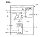
図4aに示される更新されたクロックゲーティングセル12aは、クロックゲーティングセル102a(CG(電流))、スキャンDフリップフロップ102b(スキャンFF)および組合せ論理102cから構成される。クロックゲーティングセルCG(電流)の最も簡単な実現形態は、ANDゲートによって提供される。ここで考慮される場合、1つのイネーブル信号は、クロック信号clk_iを制御する。図4aの特定の例では、クロックゲーティングセル102a(CG(電流))は、入力として、第1のクロック信号(clk_i)、機能イネーブル信号(FE)およびシフトイネーブル信号(SE)を使用する。クロックゲーティングセル102a(CG(電流))の出力信号は、clk_oで示される。例えば、信号clk_iは、これらに限定されないが、機能上の(非テスト)動作の間の高速/マスタクロック信号、スキャンテストのキャプチャサイクルの間の高速/マスタクロック信号、または、スキャンテストの初期化サイクルの間のスキャンシフトクロック信号(シフトイン、シフトアウト)であり得る。
The updated
以下では、以前に説明されたクロックゲーティングセル102a(CG(電流))は、「従来のクロックゲーティングセルの一例」で示される。それは、例えば、以下の真理値表によって特徴付けられる(表1では、xは、0または1を示す)。
In the following, the

従来のクロックゲーティングセルの1つの特定の実現形態は、制限することなく、図4bに示されている。それは、ORゲート102e、ラッチ102dおよびANDゲート102fによって組み立てられている。この従来のクロックゲーティングセルは、テスト設計に一般的に使用されるが、その理由は、シフトイネーブル信号(SE)の方が、機能イネーブル信号(FE)と比較して、ATPGツールによる制御がはるかに簡単であるためである。具体的には、SE入力の包含により、FE信号とは無関係に、スキャンテスト信号を有効にすることが可能になる。図4bに示される従来のクロックゲーティングセルの特定の実施形態のラッチは、以下の利益のために使用される。クロック信号clk_i=0である限り、出力クロック信号(clk_o)はOFFであり、すなわち、clk_o=0である。クロック信号clk_iが0から1に変化すると、ラッチは、そのD入力で状態を保持し、クロックゲーティングセルでのタイミング問題を減少させる。clk_i=1である限り、出力クロック信号clk_oは、FEまたはSEの変化による影響を受けない。
One particular implementation of a conventional clock gating cell is shown in FIG. 4b without limitation. It is assembled by an
本開示では、特定の従来のクロックゲーティングセルは例示として考慮されているが、従来のクロックゲーティングセルCG(電流)をテスト設計で頻繁に使用される他の任意のタイプのクロックゲーティングセルに置き換えるかまたは適合させることは当業者にとって造作もないことであるはずである。この意味で、図4bのラッチを、例えば、フリップフロップに置き換えることも、従来のクロックゲーティングセルの別の実現形態では、ORゲートをラッチの後方に配置することもできる。従来のクロックゲーティングセルの提示された実現形態(図4b)の多くの小規模な変更形態は、本開示で使用することができ、当業者にはよく知られている。 In this disclosure, certain conventional clock gating cells are considered by way of example, but the conventional clock gating cell CG (current) is any other type of clock gating cell that is frequently used in test designs. Substituting or adapting to should not be a feature to those skilled in the art. In this sense, the latch of FIG. 4b can be replaced by, for example, a flip-flop, or in another implementation of a conventional clock gating cell, an OR gate can be placed behind the latch. Many minor variations of the proposed implementation of a conventional clock gating cell (FIG. 4b) can be used in the present disclosure and are well known to those skilled in the art.
図4aの更新されたクロックゲーティングセルのスキャンDフリップフロップ102b(スキャンFF)は、スキャンシフト動作の間にシフトイン(SI)信号によって制御される。これは、特に、一方では、より優れたおよびより簡単なATPGの可制御性ひいてはより高いテスト網羅率をもたらし、他方では、スキャンテストの間の電力消費量の低減をもたらす。この特定の実施形態では、スキャンフリップフロップのQ出力は、スキャンシフト出力(SO)信号を出力する。
The updated clock gating cell scan D flip-
所定の例の組合せ論理102cは、1つのインバータ、2つのORゲートおよび2つのANDゲートを含み、図4aに示されるように接続される。
The given
本開示の第1の例示的な更新されたクロックゲーティングセル12a(CG_1)は、6つの入力、すなわち、クロック信号clk_i、機能イネーブル信号FE、シフトイネーブル信号SE、遅延テストイネーブル信号DT、スキャンシフト入力信号SI、および、スキャンモードの間にスキャンフリップフロップ(スキャンFF)をリセットするリセット信号(reset)を所有する。更新されたクロックゲーティングセルCG_1は、クロック信号clk_oおよびスキャンシフト出力(SO)信号を出力する。図4aの論理を考慮すると、CG_1の真理値表は、表2で得られるような結果となる。
The first exemplary updated
表2では、xは、0または1を示す。その上、表2を考慮すると、DT=0、SE=0(例えば、機能上の動作における)によって特徴付けられたフェーズでは、出力クロック信号clk_oは、機能イネーブル信号FEによって完全に制御されることが分かる。SE=1(例えば、スキャンテストのシフトフェーズ)によって特徴付けられたフェーズのいずれかの間は、更新されたクロックゲーティングセルCG_1は、クロック入力信号clk_i(これに限定されないが、スキャンシフトクロック入力信号であり得る)に完全にトランスペアレントである。DT=1、SE=0(例えば、実動作速度キャプチャサイクル)によって特徴付けられたフェーズの間は、出力クロック信号clk_oは、例えばスキャンテストのシフトインサイクルにおける信号SIによって設定されている、スキャンフリップフロップ(スキャンFF)によって制御される。この最終フェーズでは、clk_iは、例えば、高速/マスタクロック信号によって得ることができる。スキャンFF=1の場合は、更新されたクロックゲーティングセルCG_1は、入力クロック信号clk_iに完全にトランスペアレントである、すなわち、スキャンFF=1に関しては、clk_o=clk_iであるが、スキャンFF=0の場合は常に、CG_1はオフ(OFF)に切り替わり、例えばスキャンテストのキャプチャサイクルの間の機能イネーブル信号とは無関係である。説明される更新されたクロックゲーティングセル12a(CG_1)を用いることで、望ましくない部分的イネーブルクロック信号は、CG_1の出力clk_oで除去される。
In Table 2, x represents 0 or 1. Moreover, considering Table 2, in the phase characterized by DT = 0, SE = 0 (eg in functional operation), the output clock signal clk_o is completely controlled by the function enable signal FE. I understand. During any of the phases characterized by SE = 1 (eg, the shift phase of the scan test), the updated clock gating cell CG_1 receives the clock input signal clk_i (but is not limited to the scan shift clock input). Fully transparent). During a phase characterized by DT = 1, SE = 0 (eg actual operating speed capture cycle), the output clock signal clk_o is set by a signal SI, for example in the shift-in cycle of the scan test. (Scan FF). In this final phase, clk_i can be obtained, for example, by a high speed / master clock signal. When scan FF = 1, the updated clock gating cell CG_1 is completely transparent to the input clock signal clk_i, ie, for scan FF = 1, clk_o = clk_i, but scan FF = 0 In all cases, CG_1 is switched off and is independent of, for example, the function enable signal during the scan test capture cycle. By using the described updated
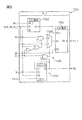
図5に示される第2の例示的な実施形態は、図4aの更新されたクロックゲーティングセルCG_1の文脈で導入された入力信号clk_i、FE、SE、DT、SI、リセットに加えて、入力信号slow_clk_en_i(これに限定されないが、デジタル回路の低速クロックイネーブル信号であり得る)を含む。更新されたクロックゲーティングセル1012a(CG_2)は、更新されたクロックゲーティングセル12a(CG_1)の文脈で説明されるような、第1および第2の従来のクロックゲーティングセル1102d、1102a(CG(電流)、例えば、図4bに示されるような)、マルチプレクサ1102e、スキャンDフリップフロップ1102b(スキャンFF)、ならびに、組合せ論理1102cから構成される。システムマルチプレクサ/クロックゲーティングセルは、「マルチプレクサタイプのクロックゲーティングセル」で一般的に示される。更新されたクロックゲーティングセルCG_2は、出力クロック信号clk_oおよびスキャンシフト出力信号SOを出力する。
The second exemplary embodiment shown in FIG. 5 has an input in addition to the input signals clk_i, FE, SE, DT, SI, reset introduced in the context of the updated clock gating cell CG_1 of FIG. 4a. Signal slow_clk_en_i (which can be, but is not limited to, a slow clock enable signal for a digital circuit). The updated
更新されたクロックゲーティングセルCG_2は、例えば、slow_clk_en_i信号(例えば、図3のCCU.slow_clk_en)の使用によって、第2のクロック信号が高速/マスタクロック信号(例えば、図3のCCU.fast_clk_o)から導出される場合に使用することができる。clk_i入力がclk_i信号と接続され、FE入力がslow_clk_en_in信号と接続される、図5の第1の従来のクロックゲーティングセル1102d(CG(電流))は、所望のクロック信号を生成する。マルチプレクサ1102eの出力は、第2の従来のクロックゲーティングセル1102a(CG(電流))の入力FEに接続される。マルチプレクサの入力信号(0または1)に応じて、マルチプレクサの出力信号は、マルチプレクサの「0」入力での信号またはマルチプレクサの「1」入力での信号のそれぞれによって得られる。スキャンフリップフロップ1102b(スキャンFF)は、図4aの更新されたクロックゲーティングセルCG_1の文脈で説明されるようなものである。
The updated clock gating cell CG_2 has a second clock signal derived from the high speed / master clock signal (for example, CCU.fast_clk_o in FIG. 3) by using, for example, the slow_clk_en_i signal (for example, CCU.slow_clk_en in FIG. 3). Can be used when derived. The first conventional
図5の組合せ論理を考慮すると、2つのANDゲート、1つのORゲートおよび1つのインバータを備えるCG_2の真理値表は、表3の通り得られる。 Considering the combinational logic of FIG. 5, a truth table of CG_2 including two AND gates, one OR gate, and one inverter is obtained as shown in Table 3.
表2と同様に、表3のxは、0または1を示す。DT=0、SE=0(例えば、機能上の動作における)によって特徴付けられたフェーズでは、出力クロック信号clk_oは、機能イネーブル信号FEによって完全に制御される。SE=1(例えば、スキャンテストのシフトフェーズ)によって特徴付けられたフェーズのいずれかの間は、更新されたクロックゲーティングセルCG_2は、クロック入力信号clk_i(これに限定されないが、スキャンシフトクロック入力信号であり得る)に完全にトランスペアレントである。DT=1、SE=0(例えば、実動作速度キャプチャサイクル)によって特徴付けられたフェーズの間は、出力クロック信号clk_oは、例えばスキャンテストのシフトインサイクルにおける信号SIによって設定されている、slow_clk_en信号とスキャンフリップフロップ(スキャンFF)の両方によって制御される。slow_clk_en信号が存在しない、すなわち、slow_clk_en=0である限り、更新されたクロックゲーティングセルCG_2はOFFであり、スキャンフリップフロップ(スキャンFF)の状態とは無関係である。slow_clk_en=1の場合、更新されたクロックゲーティングセルCG_2は、スキャンFFが設定されている、すなわち、スキャンFF=1の場合は、クロック信号clk_iに完全にトランスペアレントであるが、スキャンFF=0の場合は、CG_2はOFFである。更新されたクロックゲーティングセルCG_2の一応用では、CG_2は、ATPGツールによる更新されたクロックゲーティングセルCG_2の出力での低速/分割クロック信号の定義を可能にする。 Similar to Table 2, x in Table 3 represents 0 or 1. In the phase characterized by DT = 0, SE = 0 (eg in functional operation), the output clock signal clk_o is completely controlled by the function enable signal FE. During any of the phases characterized by SE = 1 (eg, the shift phase of the scan test), the updated clock gating cell CG_2 receives the clock input signal clk_i (but is not limited to the scan shift clock input). Fully transparent). During the phase characterized by DT = 1, SE = 0 (eg, actual operating speed capture cycle), the output clock signal clk_o is set by the signal SI, eg, in the shift-in cycle of the scan test, the slow_clk_en signal And a scan flip-flop (scan FF). As long as the slow_clk_en signal is not present, that is, as long as slow_clk_en = 0, the updated clock gating cell CG_2 is OFF and is independent of the state of the scan flip-flop (scan FF). When slow_clk_en = 1, the updated clock gating cell CG_2 has a scan FF, that is, when the scan FF = 1, the clock signal clk_i is completely transparent, but the scan FF = 0 In this case, CG_2 is OFF. In one application of the updated clock gating cell CG_2, CG_2 allows the definition of the slow / divided clock signal at the output of the updated clock gating cell CG_2 by the ATPG tool.
同じまたは他の応用では、更新されたクロックゲーティングセルCG_1またはCG_2の各々は、SI信号に応じて、スキャンモードごとに一度、個別にオンにすることも、オフに切り替えることもできる。この個別の制御を用いることで、スキャンテストの間の電力消費量の低減が可能である。 In the same or other applications, each of the updated clock gating cells CG_1 or CG_2 can be individually turned on or switched off once for each scan mode, depending on the SI signal. By using this individual control, the power consumption during the scan test can be reduced.
図6は、上記で提供される説明による、更新されたクロックゲーティングセルCG_1またはCG_2を含むトップレベルの実装形態の一例を示す。具体的に示すため、しかし適用性を制約することなく、第1(例えば、高速)のクロックドメインで動作する第1の知的財産(IP)モジュール601aおよび第2(例えば、低速または分割)のクロックドメインで動作する第2のIPモジュール601bが示されている。クロック信号のいずれも、クロック制御ユニット603によって生成される。高速クロック信号は、fast_clk_oで与えられ、第1のIPモジュール601aおよび第2のIPモジュール601bに対するクロックイネーブル信号は、fast_clk_en_oおよびslow_clk_en_oのそれぞれで示される。
FIG. 6 shows an example of a top-level implementation that includes an updated clock gating cell CG_1 or CG_2 according to the description provided above. To illustrate, but without restricting applicability, a first intellectual property (IP)
第1のIPモジュール601aは、例示として、回路のいかなる段でも、従来のクロックゲーティングセルのいくつかまたはすべてを置き換えた、タイプCG_1の更新されたクロックゲーティングセルを含む。従来のクロックゲーティングセルの入力に既に存在する入力信号clk_i、FEおよびSEに加えて、第1のIPモジュールにおける更新されたクロックゲーティングセルの各々は、遅延テストイネーブル信号(delay_test)、スキャンシフト入力信号(SI)およびリセット信号(reset)を受信する。delay_test=1は、遅延故障テストの実動作速度キャプチャサイクルを定義する。スキャンシフト入力信号は、特に、例えば、内部スキャンフリップフロップを制御することによって、更新されたクロックゲーティングセルをオンにするかまたはオフに切り替えるために使用される。最終的に、リセット信号(reset)は、異なるスキャンモードの間に既存のシステムをリセットするために使用される。
The
第2のIPモジュール601bは、具体的に示すため、しかし制限することなく、一次段のクロックゲーティングセルとして、上記で詳述されるようなタイプCG_1の1つの更新されたクロックゲーティングセル、および、第2およびそれ以上の段のクロックゲーティングセルとして、上記で説明されるようなタイプCG_2の更新されたクロックゲーティングセルから構成される。タイプCG_1の更新されたクロックゲーティングセルの入力に存在し、既に論じられたclk_i、FE、SE、DT、SIおよびリセット入力信号に加えて、第2のIPモジュールにおけるタイプCG_2の更新されたクロックゲーティングセルの各々は、入力slow_clk_en_iで低速クロックイネーブル信号(例えば、slow_clk_en_o)を受信する。上記で説明されるように、slow_clk_en_iでの入力は、delay_test=1の場合の更新されたクロックゲーティングセルの挙動にのみ影響を及ぼす。この場合、slow_clk_en_iでの入力は、更新されたクロックゲーティングセルがONであるという条件の下、出力クロック信号clk_oの波形を決定する。クロック信号の所望の波形が生成された時点で、スキャンチェーン内の高次段(第2およびそれ以上)の更新されたクロックゲーティングセルがタイプCG_1のものであるということは、必須ではなく、十分である。
The
表2および表3で与えられる更新されたクロックゲーティングセルCG_1およびCG_2のそれぞれの挙動のため、機能上の動作およびテスト動作の両方の各フェーズでの出力クロック信号clk_oは、個々の更新されたクロックゲーティングセルの各々での入力信号による制御が可能である。具体的には、DT=1(これに限定されないが、実動作速度遅延故障テストのキャプチャサイクルを含む)でのフェーズの間の出力クロック信号clk_oは、スキャンチェーンの各段での入力クロック信号(fast_clk_o)およびクロックイネーブル信号(例えば、fast_clk_en_o、slow_clk_en_o)によって完全に制御される。図6に示される例示的な実施形態によれば、一次クロックゲーティングセルの出力clk_oで定義されたフェーズDT=1の間のクロック信号は、ONに設定された高次段(第2およびそれ以上)のクロックゲーティングセルでは変化しない。その上、クロック信号の歪み波形(図1に例示的に示されるような、事例3−1、3−2、3−3、7−1、7−2、7−3の部分的イネーブルクロック信号)を除去することができる。更新されたクロックゲーティングセルの各々での明確に定義された出力クロック信号のため、ATPGツールは、入力FEでの機能イネーブル信号に関わらず、キャプチャフェーズの間のこれらのクロックゲーティングセルの各々の出力でのクロック信号を定義することができるようになる。本開示による更新されたクロックゲーティングセルの使用のこの最後の含意は、結果的に、テスト網羅率の増加をもたらす。その上、更新されたクロックゲーティングセルの応用により、特に、各IPモジュールに対する制御可能なクロック信号の定義が可能になるため、テスト網羅率をさらに増加することができるが、その理由は、クロックードメインスイッチングを除去することも、抑制することもできるためである。具体的には、高速ドメインに発生した故障が低速ドメインでテストされること(テスト回避を招く;クロック信号の歪み波形は、図1の事例3−1に示される)およびその逆(過度のテストを招く;クロック信号の歪み波形は、図1の事例5−1に示される)を除去することができる。 Due to the respective behavior of the updated clock gating cells CG_1 and CG_2 given in Tables 2 and 3, the output clock signal clk_o in each phase of both functional and test operations is updated individually. Control by an input signal in each of the clock gating cells is possible. Specifically, the output clock signal clk_o during the phase at DT = 1 (including but not limited to the capture cycle of the actual operating speed delay fault test) is the input clock signal at each stage of the scan chain ( fast_clk_o) and clock enable signals (eg, fast_clk_en_o, slow_clk_en_o). According to the exemplary embodiment shown in FIG. 6, the clock signal during phase DT = 1 defined by the output clk_o of the primary clock gating cell is a high order stage (second and The above does not change in the clock gating cell. In addition, the distortion waveform of the clock signal (partial enable clock signals of cases 3-1, 3-2, 3-3, 7-1, 7-2, 7-3, as exemplarily shown in FIG. ) Can be removed. Because of the well-defined output clock signal on each of the updated clock gating cells, the ATPG tool will enable each of these clock gating cells during the capture phase regardless of the function enable signal at the input FE. The clock signal at the output of can be defined. This last implication of the use of updated clock gating cells according to the present disclosure results in increased test coverage. In addition, the application of the updated clock gating cell allows the definition of a controllable clock signal for each IP module in particular, which can further increase the test coverage, because the clock This is because the co-domain switching can be removed or suppressed. Specifically, faults occurring in the high speed domain are tested in the low speed domain (leading to test avoidance; the distortion waveform of the clock signal is shown in case 3-1 of FIG. 1) and vice versa (excessive testing The distortion waveform of the clock signal can be eliminated) as shown in case 5-1 of FIG.
更新されたクロックゲーティングセルの使用の別の利益は、スキャンフリップフロップによるそれらの個々の可制御性により生じ得る。スキャンテストの間の電力消費量は、減少させた数の更新されたクロックゲーティングセルのみをオンに切り替えることによって低減することができる。スキャンテストの間の電力消費量を低減するため、ATPGツールには、閾値として、スキャンテストの間にオンにすべき最大数の更新されたクロックゲーティングセルを与えることができる。 Another benefit of the use of updated clock gating cells can arise from their individual controllability by the scan flip-flops. The power consumption during the scan test can be reduced by switching on only a reduced number of updated clock gating cells. To reduce power consumption during the scan test, the ATPG tool can be provided with a maximum number of updated clock gating cells to be turned on during the scan test as a threshold.
本開示のさらなる利益は、例えば、回路、回路要素、システム要素、モジュールなどにおけるその高速のおよび簡単な実装形態であり得る。従来のクロックゲーティングセルの各々は、更新されたクロックゲーティングセルのうちの1つ(例えば、CG_1、CG_2)に置き換えることができる。従来のクロックゲーティングセルを更新されたクロックゲーティングセルに置き換えることは、例えば、自動設計変更指示(ECO)スクリプトによって達成することができる。 A further benefit of the present disclosure may be its fast and simple implementation in, for example, circuits, circuit elements, system elements, modules, etc. Each of the conventional clock gating cells can be replaced with one of the updated clock gating cells (eg, CG_1, CG_2). Replacing a conventional clock gating cell with an updated clock gating cell can be accomplished, for example, by an automatic design change instruction (ECO) script.
本開示はある実施形態を参照して説明されてきたが、当業者であれば、本開示の範囲から逸脱することなく、様々な変更を行うことができ、均等物を代用できることが理解されよう。それに加えて、特定の状況または材料を本開示の教示に適合させるため、その範囲から逸脱することなく、多くの修正を行うことができる。したがって、本開示は開示される特定の実施形態に限定されないが、本開示は添付の特許請求の範囲内に収まるすべての実施形態を含むことが意図される。 Although the present disclosure has been described with reference to certain embodiments, those skilled in the art will recognize that various modifications can be made and equivalents can be substituted without departing from the scope of the disclosure. . In addition, many modifications may be made to adapt a particular situation or material to the teachings of the disclosure without departing from the scope thereof. Accordingly, the disclosure is not limited to the particular embodiments disclosed, but the disclosure is intended to include all embodiments that fall within the scope of the appended claims.
1 システムオンチップ(SoC)
2a、2b、2c、2d クロックゲーティングセル
3 クロック制御ユニット
4b、4d 部分的イネーブル信号
5b、5d 機能的制御
12a クロックゲーティングセル
102a クロックゲーティングセル
102b スキャンDフリップフロップ
102c 組合せ論理
102d ラッチ
102e ORゲート
102f ANDゲート
601a IP(高速クロックドメイン)
601b IP(低速または分割クロックドメイン)
603 クロック制御ユニット
1012a クロックゲーティングセル
1102a、1102d クロックゲーティングセル
1102b スキャンDフリップフロップ
1102c 組合せ論理
1102e マルチプレクサ
1 System-on-chip (SoC)
2a, 2b, 2c, 2d Clock gating cell 3
601b IP (low speed or split clock domain)
603
Claims (19)
(a)前記スキャンテストのいかなる段階でも、各クロックゲーティングセルでクロック信号の制御可能な波形を出力するステップと、
(b)キャプチャサイクルの間に、各クロックゲーティングセルで部分的イネーブルクロック信号を除去するステップと
を含む、方法。 A method applied to a clock system of a scan circuit of a scan test including one or more clock gating cells,
(A) outputting a controllable waveform of the clock signal at each clock gating cell at any stage of the scan test;
(B) removing a partial enable clock signal at each clock gating cell during a capture cycle.
前記テストの前記キャプチャサイクルの間に、部分的イネーブルクロック信号を除去する
ように構成される、クロックゲーティングセル。 Output a controllable waveform of the clock signal during the capture cycle of the delay fault scan structure test,
A clock gating cell configured to remove a partial enable clock signal during the capture cycle of the test.
(a)前記クロックゲーティングセルの各々は、個別に制御可能であるように構成され、
(b)前記クロックゲーティングセルの各々は、遅延故障スキャン構造テストのキャプチャサイクルの間にクロック信号の制御可能な波形を出力するように構成され、
(c)前記クロックゲーティングセルの各々は、前記テストの前記キャプチャサイクルの間に部分的イネーブルクロック信号を除去するように構成される、
スキャン回路。 A scan circuit comprising one or more clock gating cells, configured to be used for scan testing;
(A) Each of the clock gating cells is configured to be individually controllable,
(B) each of the clock gating cells is configured to output a controllable waveform of a clock signal during a capture cycle of a delay fault scan structure test;
(C) each of the clock gating cells is configured to remove a partial enable clock signal during the capture cycle of the test;
Scan circuit.
Applications Claiming Priority (2)
| Application Number | Priority Date | Filing Date | Title |
|---|---|---|---|
| US14/083,624 | 2013-11-19 | ||
| US14/083,624 US9377511B2 (en) | 2013-11-19 | 2013-11-19 | Coverage enhancement and power aware clock system for structural delay-fault test |
Publications (2)
| Publication Number | Publication Date |
|---|---|
| JP2015099146A true JP2015099146A (en) | 2015-05-28 |
| JP2015099146A5 JP2015099146A5 (en) | 2017-01-26 |
Family
ID=53174545
Family Applications (1)
| Application Number | Title | Priority Date | Filing Date |
|---|---|---|---|
| JP2014228018A Pending JP2015099146A (en) | 2013-11-19 | 2014-11-10 | Coverage enhancement and power aware clock system for structural delay-fault test |
Country Status (4)
| Country | Link |
|---|---|
| US (1) | US9377511B2 (en) |
| JP (1) | JP2015099146A (en) |
| KR (1) | KR101690376B1 (en) |
| DE (1) | DE102014017099A1 (en) |
Families Citing this family (3)
| Publication number | Priority date | Publication date | Assignee | Title |
|---|---|---|---|---|
| US10447461B2 (en) * | 2015-12-01 | 2019-10-15 | Infineon Technologies Austria Ag | Accessing data via different clocks |
| CN106992770B (en) * | 2016-01-21 | 2021-03-30 | 华为技术有限公司 | Clock circuit and method for transmitting clock signal |
| KR102630258B1 (en) * | 2021-10-26 | 2024-01-25 | 연세대학교 산학협력단 | Circuit and method for capture power reduction in logic bist |
Citations (9)
| Publication number | Priority date | Publication date | Assignee | Title |
|---|---|---|---|---|
| US20020162065A1 (en) * | 2001-04-26 | 2002-10-31 | Shinji Kashiwagi | Scan test circuit |
| US6880137B1 (en) * | 2001-08-03 | 2005-04-12 | Inovys | Dynamically reconfigurable precision signal delay test system for automatic test equipment |
| US20050138511A1 (en) * | 2003-11-24 | 2005-06-23 | Robert Benware | Self-timed scan circuit for ASIC fault testing |
| WO2006064300A1 (en) * | 2004-12-13 | 2006-06-22 | Infineon Technologies Ag | Circuitry and method for an at-speed scan test |
| US20100306607A1 (en) * | 2009-05-28 | 2010-12-02 | Renesas Electronics Corporation | Semiconductor integrated circuit and method of testing the same |
| US20100332928A1 (en) * | 2009-06-26 | 2010-12-30 | Wei Li | Scalable scan system for system-on-chip design |
| US20110296265A1 (en) * | 2010-05-25 | 2011-12-01 | Freescale Semiconductor, Inc | System for testing integrated circuit with asynchronous clock domains |
| JP2013156073A (en) * | 2012-01-27 | 2013-08-15 | Renesas Electronics Corp | Semiconductor device |
| US20130254609A1 (en) * | 2012-03-22 | 2013-09-26 | Renesas Electronics Corporation | Scan test circuit, test pattern generation control circuit, and scan test control method |
Family Cites Families (8)
| Publication number | Priority date | Publication date | Assignee | Title |
|---|---|---|---|---|
| US8091002B2 (en) * | 2001-02-15 | 2012-01-03 | Syntest Technologies, Inc. | Multiple-capture DFT system to reduce peak capture power during self-test or scan test |
| JP2005032102A (en) * | 2003-07-09 | 2005-02-03 | Matsushita Electric Ind Co Ltd | Scan test design method, scan test circuit, scan flip-flop circuit, cad program for scan test circuit insertion, large-scale integrated circuit, and mobile digital device |
| US7613971B2 (en) * | 2005-02-08 | 2009-11-03 | Nec Electronics Corporation | Semiconductor integrated circuit with delay test circuit, and method for testing semiconductor integrated circuit |
| TW200801550A (en) * | 2006-01-06 | 2008-01-01 | Koninkl Philips Electronics Nv | IC testing methods and apparatus |
| US20080282122A1 (en) * | 2007-05-09 | 2008-11-13 | Amar Guettaf | Single scan clock in a multi-clock domain |
| US20100138709A1 (en) * | 2008-10-22 | 2010-06-03 | Laung-Terng Wang | Method and apparatus for delay fault coverage enhancement |
| WO2012046602A1 (en) * | 2010-10-05 | 2012-04-12 | 国立大学法人 九州工業大学 | Fault detection system, extraction device, fault detection method, program, and recording medium |
| US8862955B2 (en) * | 2010-12-29 | 2014-10-14 | Stmicroelectronics S.R.L. | Apparatus for at-speed testing, in inter-domain mode, of a multi-clock-domain digital integrated circuit according to BIST or SCAN techniques |
-
2013
- 2013-11-19 US US14/083,624 patent/US9377511B2/en active Active
-
2014
- 2014-11-10 JP JP2014228018A patent/JP2015099146A/en active Pending
- 2014-11-18 KR KR1020140161033A patent/KR101690376B1/en active IP Right Grant
- 2014-11-19 DE DE102014017099.3A patent/DE102014017099A1/en not_active Withdrawn
Patent Citations (12)
| Publication number | Priority date | Publication date | Assignee | Title |
|---|---|---|---|---|
| US20020162065A1 (en) * | 2001-04-26 | 2002-10-31 | Shinji Kashiwagi | Scan test circuit |
| JP2002323540A (en) * | 2001-04-26 | 2002-11-08 | Nec Corp | Circuit for scan test |
| US6880137B1 (en) * | 2001-08-03 | 2005-04-12 | Inovys | Dynamically reconfigurable precision signal delay test system for automatic test equipment |
| US20050138511A1 (en) * | 2003-11-24 | 2005-06-23 | Robert Benware | Self-timed scan circuit for ASIC fault testing |
| WO2006064300A1 (en) * | 2004-12-13 | 2006-06-22 | Infineon Technologies Ag | Circuitry and method for an at-speed scan test |
| US20100306607A1 (en) * | 2009-05-28 | 2010-12-02 | Renesas Electronics Corporation | Semiconductor integrated circuit and method of testing the same |
| JP2010276479A (en) * | 2009-05-28 | 2010-12-09 | Renesas Electronics Corp | Semiconductor integrated circuit and method of testing the same |
| US20100332928A1 (en) * | 2009-06-26 | 2010-12-30 | Wei Li | Scalable scan system for system-on-chip design |
| US20110296265A1 (en) * | 2010-05-25 | 2011-12-01 | Freescale Semiconductor, Inc | System for testing integrated circuit with asynchronous clock domains |
| JP2013156073A (en) * | 2012-01-27 | 2013-08-15 | Renesas Electronics Corp | Semiconductor device |
| US20130254609A1 (en) * | 2012-03-22 | 2013-09-26 | Renesas Electronics Corporation | Scan test circuit, test pattern generation control circuit, and scan test control method |
| JP2013224917A (en) * | 2012-03-22 | 2013-10-31 | Renesas Electronics Corp | Scan test circuit, test pattern generation control circuit, and scan test control method |
Also Published As
| Publication number | Publication date |
|---|---|
| KR101690376B1 (en) | 2016-12-27 |
| DE102014017099A1 (en) | 2015-05-21 |
| US9377511B2 (en) | 2016-06-28 |
| US20150143189A1 (en) | 2015-05-21 |
| KR20150058060A (en) | 2015-05-28 |
Similar Documents
| Publication | Publication Date | Title |
|---|---|---|
| US10931264B2 (en) | Low-power flip flop circuit | |
| US9322876B2 (en) | Control test point for timing stability during scan capture | |
| US9366727B2 (en) | High density low power scan flip-flop | |
| JP5256840B2 (en) | Logic circuit | |
| US9222979B2 (en) | On-chip controller and a system-on-chip | |
| US7761755B1 (en) | Circuit for and method of testing for faults in a programmable logic device | |
| US8479068B2 (en) | Decoded register outputs enabling test clock to selected asynchronous domains | |
| US7457998B1 (en) | Scan register and methods of using the same | |
| US20090300448A1 (en) | Scan flip-flop device | |
| US8671320B2 (en) | Integrated circuit comprising scan test circuitry with controllable number of capture pulses | |
| KR20050112972A (en) | Semiconductor integrated circuit device having scan flip-flop circuit | |
| KR20080031654A (en) | Semiconductor integrated circuit and testing method | |
| US9891279B2 (en) | Managing IR drop | |
| JP2015099146A (en) | Coverage enhancement and power aware clock system for structural delay-fault test | |
| JP5651058B2 (en) | Scan flip-flop circuit, scan test circuit and control method thereof | |
| US20150061740A1 (en) | Scannable flop with a single storage element | |
| US8832510B2 (en) | Circuit to reduce peak power during transition fault testing of integrated circuit | |
| US9612280B2 (en) | Partial scan cell | |
| JP2014202532A (en) | Latch circuit, scan test object circuit, semiconductor integrated circuit and control method for latch circuit | |
| JP2015099146A5 (en) | ||
| JP5383588B2 (en) | Scan test circuit, semiconductor integrated circuit | |
| US20150193564A1 (en) | System and method for using clock chain signals of an on-chip clock controller to control cross-domain paths | |
| JP2976937B2 (en) | Scan test circuit | |
| EP1508812B1 (en) | Scan-test method and circuit using a substitute enable signal | |
| JP5231065B2 (en) | Scan flip-flop circuit |
Legal Events
| Date | Code | Title | Description |
|---|---|---|---|
| A977 | Report on retrieval |
Free format text: JAPANESE INTERMEDIATE CODE: A971007 Effective date: 20150911 |
|
| A131 | Notification of reasons for refusal |
Free format text: JAPANESE INTERMEDIATE CODE: A131 Effective date: 20150929 |
|
| A601 | Written request for extension of time |
Free format text: JAPANESE INTERMEDIATE CODE: A601 Effective date: 20160104 |
|
| A601 | Written request for extension of time |
Free format text: JAPANESE INTERMEDIATE CODE: A601 Effective date: 20160129 |
|
| A521 | Request for written amendment filed |
Free format text: JAPANESE INTERMEDIATE CODE: A523 Effective date: 20160224 |
|
| A131 | Notification of reasons for refusal |
Free format text: JAPANESE INTERMEDIATE CODE: A131 Effective date: 20160809 |
|
| A601 | Written request for extension of time |
Free format text: JAPANESE INTERMEDIATE CODE: A601 Effective date: 20161109 |
|
| A524 | Written submission of copy of amendment under article 19 pct |
Free format text: JAPANESE INTERMEDIATE CODE: A524 Effective date: 20161209 |
|
| A02 | Decision of refusal |
Free format text: JAPANESE INTERMEDIATE CODE: A02 Effective date: 20170606 |