JP2015096878A - Optical reception module and optical transmission module - Google Patents
Optical reception module and optical transmission module Download PDFInfo
- Publication number
- JP2015096878A JP2015096878A JP2013236514A JP2013236514A JP2015096878A JP 2015096878 A JP2015096878 A JP 2015096878A JP 2013236514 A JP2013236514 A JP 2013236514A JP 2013236514 A JP2013236514 A JP 2013236514A JP 2015096878 A JP2015096878 A JP 2015096878A
- Authority
- JP
- Japan
- Prior art keywords
- light
- light receiving
- optical
- lens
- deviation
- Prior art date
- Legal status (The legal status is an assumption and is not a legal conclusion. Google has not performed a legal analysis and makes no representation as to the accuracy of the status listed.)
- Pending
Links
- 230000003287 optical effect Effects 0.000 title claims abstract description 103
- 230000005540 biological transmission Effects 0.000 title claims abstract description 15
- 239000000758 substrate Substances 0.000 claims abstract description 45
- 239000004065 semiconductor Substances 0.000 claims abstract description 30
- 230000009467 reduction Effects 0.000 abstract description 2
- 238000010586 diagram Methods 0.000 description 11
- 239000003795 chemical substances by application Substances 0.000 description 7
- 230000004048 modification Effects 0.000 description 7
- 238000012986 modification Methods 0.000 description 7
- 239000013307 optical fiber Substances 0.000 description 7
- 239000000853 adhesive Substances 0.000 description 6
- 230000001070 adhesive effect Effects 0.000 description 6
- 230000000694 effects Effects 0.000 description 6
- NJPPVKZQTLUDBO-UHFFFAOYSA-N novaluron Chemical compound C1=C(Cl)C(OC(F)(F)C(OC(F)(F)F)F)=CC=C1NC(=O)NC(=O)C1=C(F)C=CC=C1F NJPPVKZQTLUDBO-UHFFFAOYSA-N 0.000 description 5
- 238000004891 communication Methods 0.000 description 3
- 230000008878 coupling Effects 0.000 description 3
- 238000010168 coupling process Methods 0.000 description 3
- 238000005859 coupling reaction Methods 0.000 description 3
- 230000006866 deterioration Effects 0.000 description 3
- 230000005684 electric field Effects 0.000 description 3
- 238000004519 manufacturing process Methods 0.000 description 3
- 230000007480 spreading Effects 0.000 description 3
- 238000005530 etching Methods 0.000 description 2
- 230000008859 change Effects 0.000 description 1
- 230000008602 contraction Effects 0.000 description 1
- 230000007774 longterm Effects 0.000 description 1
- 239000000463 material Substances 0.000 description 1
- 238000000034 method Methods 0.000 description 1
- 230000008569 process Effects 0.000 description 1
- 238000012545 processing Methods 0.000 description 1
- 238000011160 research Methods 0.000 description 1
- 230000035945 sensitivity Effects 0.000 description 1
- 230000008054 signal transmission Effects 0.000 description 1
- 125000006850 spacer group Chemical group 0.000 description 1
- 230000001629 suppression Effects 0.000 description 1
Images


Classifications
-
- G—PHYSICS
- G02—OPTICS
- G02B—OPTICAL ELEMENTS, SYSTEMS OR APPARATUS
- G02B6/00—Light guides; Structural details of arrangements comprising light guides and other optical elements, e.g. couplings
- G02B6/24—Coupling light guides
- G02B6/42—Coupling light guides with opto-electronic elements
- G02B6/4201—Packages, e.g. shape, construction, internal or external details
- G02B6/4204—Packages, e.g. shape, construction, internal or external details the coupling comprising intermediate optical elements, e.g. lenses, holograms
-
- G—PHYSICS
- G01—MEASURING; TESTING
- G01J—MEASUREMENT OF INTENSITY, VELOCITY, SPECTRAL CONTENT, POLARISATION, PHASE OR PULSE CHARACTERISTICS OF INFRARED, VISIBLE OR ULTRAVIOLET LIGHT; COLORIMETRY; RADIATION PYROMETRY
- G01J1/00—Photometry, e.g. photographic exposure meter
- G01J1/02—Details
- G01J1/029—Multi-channel photometry
-
- G—PHYSICS
- G01—MEASURING; TESTING
- G01J—MEASUREMENT OF INTENSITY, VELOCITY, SPECTRAL CONTENT, POLARISATION, PHASE OR PULSE CHARACTERISTICS OF INFRARED, VISIBLE OR ULTRAVIOLET LIGHT; COLORIMETRY; RADIATION PYROMETRY
- G01J1/00—Photometry, e.g. photographic exposure meter
- G01J1/02—Details
- G01J1/0204—Compact construction
-
- G—PHYSICS
- G01—MEASURING; TESTING
- G01J—MEASUREMENT OF INTENSITY, VELOCITY, SPECTRAL CONTENT, POLARISATION, PHASE OR PULSE CHARACTERISTICS OF INFRARED, VISIBLE OR ULTRAVIOLET LIGHT; COLORIMETRY; RADIATION PYROMETRY
- G01J1/00—Photometry, e.g. photographic exposure meter
- G01J1/02—Details
- G01J1/0214—Constructional arrangements for removing stray light
-
- G—PHYSICS
- G01—MEASURING; TESTING
- G01J—MEASUREMENT OF INTENSITY, VELOCITY, SPECTRAL CONTENT, POLARISATION, PHASE OR PULSE CHARACTERISTICS OF INFRARED, VISIBLE OR ULTRAVIOLET LIGHT; COLORIMETRY; RADIATION PYROMETRY
- G01J1/00—Photometry, e.g. photographic exposure meter
- G01J1/02—Details
- G01J1/04—Optical or mechanical part supplementary adjustable parts
- G01J1/0407—Optical elements not provided otherwise, e.g. manifolds, windows, holograms, gratings
- G01J1/0411—Optical elements not provided otherwise, e.g. manifolds, windows, holograms, gratings using focussing or collimating elements, i.e. lenses or mirrors; Aberration correction
-
- G—PHYSICS
- G02—OPTICS
- G02B—OPTICAL ELEMENTS, SYSTEMS OR APPARATUS
- G02B6/00—Light guides; Structural details of arrangements comprising light guides and other optical elements, e.g. couplings
- G02B6/24—Coupling light guides
- G02B6/42—Coupling light guides with opto-electronic elements
- G02B6/4201—Packages, e.g. shape, construction, internal or external details
- G02B6/4204—Packages, e.g. shape, construction, internal or external details the coupling comprising intermediate optical elements, e.g. lenses, holograms
- G02B6/4215—Packages, e.g. shape, construction, internal or external details the coupling comprising intermediate optical elements, e.g. lenses, holograms the intermediate optical elements being wavelength selective optical elements, e.g. variable wavelength optical modules or wavelength lockers
-
- G—PHYSICS
- G02—OPTICS
- G02B—OPTICAL ELEMENTS, SYSTEMS OR APPARATUS
- G02B6/00—Light guides; Structural details of arrangements comprising light guides and other optical elements, e.g. couplings
- G02B6/24—Coupling light guides
- G02B6/42—Coupling light guides with opto-electronic elements
- G02B6/4201—Packages, e.g. shape, construction, internal or external details
- G02B6/4249—Packages, e.g. shape, construction, internal or external details comprising arrays of active devices and fibres
- G02B6/425—Optical features
-
- G—PHYSICS
- G02—OPTICS
- G02B—OPTICAL ELEMENTS, SYSTEMS OR APPARATUS
- G02B3/00—Simple or compound lenses
- G02B3/0006—Arrays
- G02B3/0037—Arrays characterized by the distribution or form of lenses
- G02B3/005—Arrays characterized by the distribution or form of lenses arranged along a single direction only, e.g. lenticular sheets
-
- G—PHYSICS
- G02—OPTICS
- G02B—OPTICAL ELEMENTS, SYSTEMS OR APPARATUS
- G02B6/00—Light guides; Structural details of arrangements comprising light guides and other optical elements, e.g. couplings
- G02B6/24—Coupling light guides
- G02B6/26—Optical coupling means
- G02B6/28—Optical coupling means having data bus means, i.e. plural waveguides interconnected and providing an inherently bidirectional system by mixing and splitting signals
- G02B6/293—Optical coupling means having data bus means, i.e. plural waveguides interconnected and providing an inherently bidirectional system by mixing and splitting signals with wavelength selective means
- G02B6/29346—Optical coupling means having data bus means, i.e. plural waveguides interconnected and providing an inherently bidirectional system by mixing and splitting signals with wavelength selective means operating by wave or beam interference
- G02B6/29361—Interference filters, e.g. multilayer coatings, thin film filters, dichroic splitters or mirrors based on multilayers, WDM filters
- G02B6/29362—Serial cascade of filters or filtering operations, e.g. for a large number of channels
- G02B6/29365—Serial cascade of filters or filtering operations, e.g. for a large number of channels in a multireflection configuration, i.e. beam following a zigzag path between filters or filtering operations
-
- G—PHYSICS
- G02—OPTICS
- G02B—OPTICAL ELEMENTS, SYSTEMS OR APPARATUS
- G02B6/00—Light guides; Structural details of arrangements comprising light guides and other optical elements, e.g. couplings
- G02B6/24—Coupling light guides
- G02B6/26—Optical coupling means
- G02B6/28—Optical coupling means having data bus means, i.e. plural waveguides interconnected and providing an inherently bidirectional system by mixing and splitting signals
- G02B6/293—Optical coupling means having data bus means, i.e. plural waveguides interconnected and providing an inherently bidirectional system by mixing and splitting signals with wavelength selective means
- G02B6/29379—Optical coupling means having data bus means, i.e. plural waveguides interconnected and providing an inherently bidirectional system by mixing and splitting signals with wavelength selective means characterised by the function or use of the complete device
- G02B6/2938—Optical coupling means having data bus means, i.e. plural waveguides interconnected and providing an inherently bidirectional system by mixing and splitting signals with wavelength selective means characterised by the function or use of the complete device for multiplexing or demultiplexing, i.e. combining or separating wavelengths, e.g. 1xN, NxM
Abstract
Description
本発明は、光受信モジュール及び光送信モジュールに関する。 The present invention relates to an optical receiver module and an optical transmitter module.
一般に、光通信などに用いられる光受信モジュール及び光送信モジュールは、受光部や発光部の他、光ファイバからの光を受光部に導くための、又は送信部からの光を光ファイバに光を導くための各種レンズを備えている。特許文献1には、このような光受信モジュール及び光送信モジュールのうち、光受信モジュールである半導体受光装置の構成が開示されている。
In general, an optical receiver module and an optical transmitter module used for optical communication or the like are used to guide light from an optical fiber to a light receiver or light from a transmitter to an optical fiber in addition to a light receiver and a light emitter. It has various lenses to guide.
また、光受信モジュール及び光送信モジュールにおいては、光反射減衰量(ORL:Optical Return Loss)と呼ばれる反射戻り光による損失があり、この損失の抑制に関し、特許文献2は、集光レンズに対して受光部面を光線に対して斜めに配置することについて開示し、特許文献3及び4は、集光レンズに対して受光部の軸をずらす配置について開示している。
Further, in the optical receiver module and the optical transmitter module, there is a loss due to reflected return light called optical return loss (ORL), and regarding the suppression of this loss,
複数のチャネルを備えた光受信モジュール及び光送信モジュールにおいては、それぞれ光の分波回路及び合波回路を有し、1本の光ファイバからの光を分波又は複数の波長領域の光を1本の光ファイバに入射させるように合波している。このため、分波回路と受光部との間、又は合波回路と発光部との間には、チャネルの数に対応する集光レンズを有するレンズアレイを備えている。このようなレンズアレイは、一体として形成され、又は1つずつ形成されたものを一体化させて用いられることが多い。一方で、このようなレンズアレイの集光レンズには、それぞれ軸ずれ及び角度ずれが発生しやすいことから、これらを高い光利用効率の状態で配置することは難しい。また、それぞれのチャネルにおいて上述の光反射減衰量を抑えたいという要請もある。 An optical receiving module and an optical transmitting module having a plurality of channels each have a light demultiplexing circuit and a multiplexing circuit, and demultiplex light from one optical fiber or 1 light in a plurality of wavelength regions. The light is combined so as to be incident on the optical fiber of the book. For this reason, a lens array having a condensing lens corresponding to the number of channels is provided between the demultiplexing circuit and the light receiving unit or between the multiplexing circuit and the light emitting unit. In many cases, such a lens array is formed as a single unit, or is formed by integrating those formed one by one. On the other hand, the condensing lenses of such a lens array are liable to cause axial misalignment and angular misalignment, respectively, so that it is difficult to arrange them with high light utilization efficiency. There is also a demand to suppress the above-mentioned light reflection attenuation amount in each channel.
このような軸ずれ及び角度ずれの調整が不十分である場合には、所望の強度で光を伝送することができずに、信号の伝達に不具合を生じる恐れがあり、特に、光受信モジュールにおいては、分波されたチャネルとは異なるチャネルの受光部に受光させてしまう光クロストークを発生させてしまう恐れもある。 If the adjustment of the axial deviation and the angular deviation is insufficient, the light cannot be transmitted with a desired intensity, and there is a risk of causing a problem in signal transmission. May cause optical crosstalk that is received by a light receiving unit of a channel different from the demultiplexed channel.
本発明は、上述の事情に鑑みてされたものであり、複数のチャネルを有する光受信モジュール又は光送信モジュールにおいて、より伝送効率の高い光受信モジュール又は光送信モジュールを提供することを目的とする。 The present invention has been made in view of the above circumstances, and an object of the present invention is to provide an optical receiver module or an optical transmitter module having higher transmission efficiency in an optical receiver module or an optical transmitter module having a plurality of channels. .
本発明の光受信モジュールは、複数の集光レンズが、互いの光軸を平行にして、一つの平面を形成するように一方向に並べられたレンズアレイと、前記集光レンズから出射される光を受光する複数の受光素子を有する受光素子アレイと、を備え、前記受光素子アレイは、前記集光レンズからの光が入射され、透過する半導体基板と、前記半導体基板を透過した光を受光し、電気信号に変換する受光部と、を有し、前記複数の集光レンズの光軸が、それぞれ対応する前記受光部の中心からのずれは、前記一方向へのずれよりも、前記一つの平面内で前記一方向に垂直な方向のずれの方が大きい、ことを特徴とする光受信モジュールである。 In the optical receiver module of the present invention, a plurality of condensing lenses are emitted from the condensing lens, a lens array in which optical axes are parallel to each other and arranged in one direction so as to form one plane. A light receiving element array having a plurality of light receiving elements for receiving light, wherein the light receiving element array receives a light from the condenser lens and transmits the semiconductor substrate, and receives light transmitted through the semiconductor substrate. A light receiving unit that converts the light into the electrical signal. The optical receiver module is characterized in that a shift in a direction perpendicular to the one direction is larger in one plane.
また、本発明の光受信モジュールにおいて、前記集光レンズから集光される光の焦点は、前記受光部よりも前記集光レンズ側に位置していてもよい。また、この場合には、前記レンズ面で集光される光の焦点は、前記半導体基板内であってもよく、更にこの場合には、前記半導体基板の前記入射側に、前記集光レンズからの光を更に前記受光部に向けて集光するレンズ面が形成されていることとしてもよい。 Moreover, the optical receiving module of this invention WHEREIN: The focus of the light condensed from the said condensing lens may be located in the said condensing lens side rather than the said light-receiving part. In this case, the focal point of the light condensed on the lens surface may be in the semiconductor substrate, and in this case, on the incident side of the semiconductor substrate, from the condenser lens. A lens surface for condensing the light toward the light receiving unit may be formed.
また、本発明の光受信モジュールは、入射した光を相互に波長が異なる複数の光に分波し、前記複数の集光レンズに出射させる光分波回路をさらに備えていてもよい。 In addition, the optical receiver module of the present invention may further include an optical demultiplexing circuit that demultiplexes incident light into a plurality of lights having mutually different wavelengths and emits them to the plurality of condenser lenses.
また、本発明の光受信モジュールは、前記レンズアレイ及び前記受光素子アレイが配置される板と、前記板と前記レンズアレイとの間に配置される支持基板と、を更に備え、前記レンズアレイの前記一方向に垂直な方向のずれは、前記板から離れる方向のずれであってもよい。 The optical receiver module of the present invention further includes a plate on which the lens array and the light receiving element array are disposed, and a support substrate disposed between the plate and the lens array. The deviation in the direction perpendicular to the one direction may be a deviation in a direction away from the plate.
また、本発明の光受信モジュールは、前記一方向のずれは、0〜10μmの範囲であり、前記一方向に垂直な方向のずれは、8〜25μmの範囲である、こととしてもよい。 In the optical receiver module of the present invention, the deviation in the one direction may be in the range of 0 to 10 μm, and the deviation in the direction perpendicular to the one direction may be in the range of 8 to 25 μm.
本発明の光送信モジュールは、複数の集光レンズが、互いの光軸を平行にして、一つの平面を形成するように一方向に並べられたレンズアレイと、前記集光レンズに入射させる光を出射する複数の発光素子からなる発光素子アレイと、を備え、前記複数の集光レンズの光軸が、それぞれ対応する前記発光素子の中心からのずれは、前記一方向へのずれよりも、前記一つの平面内で前記一方向に垂直な方向のずれの方が大きい、ことを特徴とする光送信モジュールである。 The optical transmission module of the present invention includes a lens array in which a plurality of condensing lenses are arranged in one direction so as to form a single plane with their optical axes parallel to each other, and light incident on the condensing lens A light-emitting element array composed of a plurality of light-emitting elements that emit light, and the optical axes of the plurality of condensing lenses are each shifted from the center of the corresponding light-emitting element more than the shift in the one direction, In the optical transmission module, the deviation in a direction perpendicular to the one direction is larger in the one plane.
本発明によれば、複数のチャネルを有する光受信モジュール又は光送信モジュールにおいて、より伝送効率の高い光受信モジュール又は光送信モジュールを提供することができる。 According to the present invention, it is possible to provide an optical receiver module or an optical transmitter module having higher transmission efficiency in an optical receiver module or an optical transmitter module having a plurality of channels.
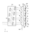
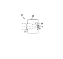
本発明の受光モジュールの実施形態を、図面を参照しながら説明する。図1は、本発明の光受信モジュールの一構成例を概略的に表す図である。この図に示される光受信モジュール100は、例えば、光通信などに用いられる光受信モジュールである。光受信モジュール100は、箱状の筐体101を備えており、筐体101の内部には支持基板103が配置されている。支持基板103には、4チャネルの光に分波する光分波回路170と、分波された光がそれぞれ入射されるレンズアレイ140と、受光した光を電気信号に変換する受光素子アレイ150と、受光素子アレイ150からボンディングワイヤ104を介して受信した電気信号を処理する回路基板102と、が取り付けられている。また、筐体101の内部にはコリメートレンズ108が配置されている。光ファイバ109から筐体101の内部に入射する光は、コリメートレンズ108によって平行光に変換され、光分波回路170、レンズアレイ140を経て、受光素子アレイ150により受光される。
An embodiment of a light receiving module of the present invention will be described with reference to the drawings. FIG. 1 is a diagram schematically illustrating a configuration example of an optical receiver module according to the present invention. The
図2は、図1の光受信モジュール100の光分波回路170、レンズアレイ140及び受光素子アレイ150の部分についての概略的に示す平面図である。コリメートレンズ108によって平行光に変換された光は、光分波回路170に入射する。入射する信号光は、例えば4つの波長領域にそれぞれ信号が重畳されており、光分波回路170に入射した光は、これらの4つの波長領域の光に分波され、レンズアレイ140の4チャネル分の集光レンズ40のそれぞれに出射される。ここで光分波回路170は、この図に示されるようなハーフミラー70を用いた空間光学型光分波回路であってもよいし、PLC(Planar Lightwave Circuit)型光分波回路その他の分波回路であってもよい。
FIG. 2 is a plan view schematically showing portions of the
レンズアレイ140の4つの集光レンズ40は、互いの光軸を平行にして、一つの平面142を形成するように一方向に並べられている。4チャネル分の集光レンズ40は、光分波回路170からの光を受光素子アレイ150に含まれる4チャネル分のそれぞれの受光素子50に向けて集光させる。なお、本実施形態においては、図1及び2に示されるように、この集光レンズ40が並ぶ一方向をX軸とし、平面142内でX軸に垂直な軸をY軸とし、支持基板103から離れる方向をプラスY方向としている。また、平面142に垂直な軸をZ軸とし、受光素子アレイ150に向う方向をプラスZ方向とている。なお、本実施形態においてはレンズアレイ140は一体的に形成されるものとしているが、一つの集光レンズ40がそれぞれ別個に形成されたものを一体的にした所謂ハイブリッドレンズアレイその他複数の集光レンズが互いの光軸を平行にして一方向に並べられたものであればよい。
The four
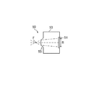
図3は、受光素子アレイ150の受光素子50について説明するための図である。受光素子50は、裏面入射型のフォトダイオードであり、半導体基板53の一方の面に受光部51が形成されており、受光部51において入射光を電気信号に変換する。本実施形態では、入射される光の波長が1.3μm帯もしくは1.55μm帯であり、半導体基板53は当該波長に対して十分な透過特性を有するInP基板とするが、これ以外の波長帯及び基板材料であってもよい。半導体基板53の他方の面には、レンズアレイ140に向かって突出した球面状の受光素子レンズ55が形成されている。例えば、受光素子レンズ55は、半導体基板53を選択的にエッチングすることによって形成される。これに限られず、例えば、半導体基板53上にレンズを別途形成してもよい。レンズアレイ140からの光は、受光素子レンズ55から半導体基板53の内側へ入射し、受光素子レンズ55によって受光部51に向けて更に集光される。しかしながら、受光素子50は、受光素子レンズ55を有さないものであってもよいし、半導体基板53の裏面に別途レンズを設けたものであってもよい。
FIG. 3 is a diagram for explaining the
なお、本明細書において「受光素子レンズ55がレンズアレイ140からの光を受光部51に向けて集光する」とは、受光素子レンズ55から受光部51までの間の光の方向が、レンズアレイ140から受光素子レンズ55までの間の光の方向よりも集光レンズ40の中心軸の方向に近づいていればよく(但し、当該中心軸上の光を除く。)、受光部51上に焦点Fが位置する場合に限定されない。
In this specification, “the light
また、ここでは「焦点」という表現で光の集光具合を説明したが、光線が最も集光するポイントである「ビームウェスト」もほぼ同義であり、「焦点の位置」ではなく「ビームウェストの位置」として考えても、本願発明の思想は変わらない。図1に戻り、レンズアレイ140は、支持基板103に対して台座105を介して接着剤等の固定剤106により固定されるが、受光部51における光反射減衰量を抑えるため、受光部51の中心よりも上方、つまりプラスY方向に集光レンズ40の中心をずらして配置している。この配置によって、集光レンズの出射光線は、受光部に対して斜めに入射し、受光部面での反射は、受光部への入射光線とは異なる方向に反射する。これにより光分波回路170から出射された光は、受光素子アレイ150のそれぞれの受光素子50に入射するが、受光部51の中心軸とずらしているため、受光部51の表面における光反射減衰量を抑えることができる。ここで、例えば図2においてX方向にレンズアレイ140を移動させて、各集光レンズ40の中心をずらすことによっても、光反射減衰量を抑えることができる。しかしながら、X方向にずらした場合には、ミラーまたは光フィルタ70の端面等で反射が発生し、反射光が他チャンネルの受光部51で受光されてしまう等の光クロストークの原因となる恐れがある。したがって、本実施形態においては、受光部51の中心軸からのY方向のずれがX方向のずれよりも大きくなるように、集光レンズ40を配置し、光反射減衰量を抑えている。これにより、光クロストークの発生による信号の劣化を抑えると共に、光反射による減衰量を抑えることができる。
In addition, although the expression of “focus” is used here to describe the degree of light collection, “beam waist”, which is the point at which light rays are most concentrated, is almost synonymous, and not “focus position” but “beam waist”. Even if considered as “position”, the idea of the present invention does not change. Returning to FIG. 1, the
ところで、受光部51上に焦点Fが位置する場合が、受光トレランスが最も広い状態である。ただし、受光面が照射される光が点に近い状態であるため、空間電荷効果により高周波特性が低下する恐れがある。空間電荷効果とは、受光部51の空乏層内部で局所的に高密度に電荷(電子正孔対)が発生することにより、外部バイアス電圧によって空乏層内部に与えられる本来の電界とは逆向きの内部電界が発生し、本来の電界強度を打ち消してしまうため、高周波特性が低下する現象である。
By the way, when the focal point F is positioned on the
図4は、図1で示された集光レンズ40と受光素子50との距離Lに対する、受光部51での受光する光のスポット径Rとの関係を説明するためのグラフである。図5A〜5Eは、図4の距離Lの範囲A〜Eにそれぞれ対応する焦点Fの位置を概略的に示す図である。図6A〜6Eは、図4の距離Lの範囲A〜Eにそれぞれ対応し、集光レンズ40の中心軸と受光部51の中心軸とのオフセットに対する、受光効率及び反射戻り光の損失についてそれぞれ示すグラフである。ここで「反射戻り光の損失」とは、入射光に対する反射戻り光の比を対数で表したものであり、この値が大きい方が、光反射減衰量を低下させることができる値である。なお、図4において、距離Lは、受光素子レンズ55の表面に焦点Fがある場合を基準(0)としており、また、受光可能なスポット径Rは、受光部51の半径を1とした場合に、例えばビームウェストのスポット径おおよそ0.18〜1.00の範囲であり、グラフにおいて最小値MIN〜最大値MAXで示されている。ここで、最小値MINは、この値に限られず、空間電荷効果の問題を回避するように定められる。
FIG. 4 is a graph for explaining the relationship between the distance L between the condensing
具体的な例として、所望の範囲の最大値MAXのスポット径Rは、例えば、一般的な25Gb/sのフォトダイオードの有効受光半径を8.0μmとすると、この有効受光半径と同程度となる。また、所望の範囲の最小値MINのスポット径Rは、例えば、空間電荷効果の問題が発生しないように定められ、フォトダイオードの性能にもよるが、おおよそ2〜3μm程度となる。 As a specific example, the spot diameter R of the maximum value MAX in the desired range is approximately the same as the effective light receiving radius when the effective light receiving radius of a general 25 Gb / s photodiode is 8.0 μm, for example. . Further, the spot diameter R of the minimum value MIN in the desired range is determined so as not to cause the space charge effect problem, and is about 2 to 3 μm, depending on the performance of the photodiode.
図4における距離Lの範囲Bは、受光部51でのスポット径Rが所望の範囲の最小値MINを下回る場合を示している。この場合、図5Bに示されるように、焦点Fは受光部51表面に位置するか、若しくはその近傍に位置している。受光部51表面でのスポット径Rが所望の範囲の最小値MINを下回る場合、上述したように空間電荷効果により高周波特性が低下する恐れがある。
A range B of the distance L in FIG. 4 indicates a case where the spot diameter R at the
図4における距離Lの範囲Aは、図5Aに示されるように、焦点Fが受光部51の集光レンズ40側とは反対側に位置する場合である。この場合にはスポット径Rは、最小値MIN以上となるが、受光素子レンズ55の面積を広く使用する必要があるため、場合によっては受光素子レンズ55より広い範囲に光が照射される恐れがある。また、受光素子レンズ55の範囲に収まる場合であっても、特にエッチング等により形成した受光素子レンズ55は、中心から離れるほど理想的な曲面から外れやすく、受光素子レンズ55の外側を使用することは結果として受光部51に照射されない光を増加させる恐れがある。したがって、受光素子レンズ55の広い範囲を利用することとなる距離Lの範囲Aは使用しない方がよいと考えられる。
A range A of the distance L in FIG. 4 is a case where the focal point F is located on the opposite side of the
図4における距離Lの位置Dは、図5Dに示されるように、焦点Fが受光素子レンズ55の表面上に位置ものであるが、この場合、受光素子レンズ55の表面で反射して、受光感度が劣化する恐れがあり、使用しない方がよいと考えられる。また、図6Dに示されるように、図6A〜6Cのグラフと比較して、受光効率が良好な範囲は狭く、反射戻り光の影響を低減させるために、集光レンズ40の中心軸を受光部の中心からオフセットしたとしても、受光効率の低下に繋がってしまう。
As shown in FIG. 5D, the position D at the distance L in FIG. 4 is the focal point F on the surface of the light
図4における距離Lの範囲Eは、図5Eに示されるように、焦点Fは集光レンズ40と受光素子50との間に位置している。この場合、集光レンズ40からの光は、集光レンズ40と受光素子レンズ55の間で焦点Fを結んだ後、次第に広がっていく状態で受光素子レンズ55に入射する。受光素子レンズ55から半導体基板53の内側に入射した光は、入射前よりも広がり率が抑えられて受光部51に至る。したがって、受光素子50に入射する光は、受光素子レンズ55により集光し切れずに、受光部51から外れる光が多くなる確率が高くなる。また、図6Eに示されるように、受光部の中心に対する集光レンズ40の中心軸のオフセットがない場合であっても受光効率が低く、距離Lの範囲Eについても使用には適さないものと考えられる。
In the range E of the distance L in FIG. 4, the focal point F is located between the
図4における距離Lの範囲Cは、図5Cに示されるように、焦点Fは半導体基板53の内側に位置している。この場合、集光レンズ40からの光は、次第に狭まっていく状態で受光素子レンズ55に入射する。受光素子レンズ55に入射した光は、半導体基板53内で焦点Fを結んだ後、次第に広がりながら受光部51に至る。スポット径Rは、最小値MINから最大値MAXの範囲であり、図6Cを参照すると、比較的大きいオフセットに対しても高い受光効率を維持しており、また、反射戻り光の影響は小さいオフセット範囲に限られている。したがってオフセットの許容範囲が広いため、反射戻り光の影響を回避しつつ、高い受光効率を得ることができる。
In the range C of the distance L in FIG. 4, the focal point F is located inside the
以上述べたように、焦点Fが半導体基板53の内側である図4の距離Lを範囲Cとすることにより、高い受光光率の範囲が広く、反射戻り光の影響を受けない範囲で光軸のオフセットを定めることができる。更に、図1で示したようにX方向よりもY方向に大きく集光レンズ40の中心軸をずらした際にも、高い受光光率を維持しつつ、光反射減衰量を抑えることができる。また、オフセット量の許容範囲が広いため、搭載位置にばらつきが生じた場合であっても、受光効率の高い範囲に収めることができる。したがって、より伝送効率の高い光受信モジュールとすることができる。
As described above, by setting the distance L in FIG. 4 where the focal point F is the inside of the
焦点Fが半導体基板53の内側に位置する距離Lの範囲Cは、レンズアレイ140と受光素子アレイ150の距離L、及び半導体基板53の厚み(受光素子レンズ55と受光部51との距離)、集光レンズ40及び受光素子レンズ55の光学パラメータにより決定される。
A range C of the distance L in which the focal point F is located inside the
図1で説明したように、レンズアレイ140を支持基板103に固定する際には台座105を介して固定剤106が用いられるが、固定剤106の厚さは、受光部51におけるトレランス範囲、集光レンズ40の製造公差、固定剤106の製造公差を加味して決定する必要がある。図5Cに示されるように、焦点Fが半導体基板53の内側の位置となるように距離Lを図4の範囲Cとして定めることにより、トレランス範囲を大きくすることができるため、オフセット量の許容範囲も広くなる。固定剤106として接着剤を使用する場合には、Y方向のうち、支持基板103から離れる方向に移動させつつ位置決めを行うと、接着剤の量を少なくすることができ、また、固定剤106の厚さを小さくすることができる。したがって、受光部51の中心軸からの集光レンズ40の中心軸のずれはY軸に関して言うとプラスY方向であることが望ましい。また、発明者らの研究によれば、Y方向のずれは、8〜25μmであれば35dB以上の光反射減衰量と0.85以上の受光効率が確保可能であり、また接着剤厚が少なくて済むため、接着剤の温度による膨張収縮量や長期信頼性による変動量が1μmと無視できるレベルで集光レンズを固定できるという結果となった。なおこの場合にはX方向のずれは、0〜10μmの範囲であれば、ほとんど結合効率が低下することなく実装することができる。本事例は、結合効率0.85、反射減衰量35dB以上を確保できる範囲を規定したが、本光受信モジュールの適用する光通信システムによっては、必要な結合効率と反射減衰量の規格が異なるため、X方向、Y方向のずれに対する許容範囲を変えてもよい。なお、台座105とレンズアレイ140との間の固定剤106は、スペーサ等であっても構わないが、製造時に微調整を行いつつ固定できる例えばUV硬化性の接着剤等が好ましい。また台座105は高さ調整のためであるため、台座105を用いないこととしてもよいし、支持基板103において予め高さが調整された形状としておいてもよい。
As described with reference to FIG. 1, when the
また、図2に示されるように、レンズアレイ140と受光素子アレイ150とが設けられるため、例えば距離Z1及びZ2が異なる等これらが互いに平行となるように配置できなかった場合には、一方の端の受光素子50では受光効率が高くても、他方の端の受光素子50では受光効率が低くなるおそれがある。しかしながら、上述のように距離Lを図4の範囲Cとしているため、オフセット量の許容範囲が広く、配置の誤差があったとしても、高い受光効率で信号を受信できる。
Further, as shown in FIG. 2, since the
図7は、上述の実施形態の第1変形例について示す図である。上述の実施形態と異なる点は、オフセットが、受光部51の中心軸より、集光レンズ40の中心軸がマイナスY方向つまり支持基板103側にずれている点であり、その他の点は同様である。このように構成した場合であっても、上述の実施形態と同様の効果を得ることができる。
FIG. 7 is a diagram illustrating a first modification of the above-described embodiment. The difference from the embodiment described above is that the offset is shifted from the central axis of the
図8は、上述の実施形態の第2変形例について示す図である。この例では光分波回路170を出射した信号光は、ミラー210に反射して支持基板103方向に向けられた後、レンズアレイ140に入射し、受光素子アレイ150で受光される。この場合にも、レンズアレイ140は、それぞれの集光レンズ40の光軸を平行にして、一つの平面142を形成するように一方向に並べられて形成されており、集光レンズ40が並ぶ方向であるX軸、平面142内でX軸と垂直な方向であるY軸、平面142に垂直なZ軸は、図8の通りに定められる。従って、上述の実施形態と同様に、受光素子50の中心から集光レンズ40の中心軸のずれは、X軸方向よりもY軸方向のずれの方が大きくなるように定められることにより、光クロストークの発生による信号の劣化を抑えると共に、光反射による減衰量を抑えることができる。また、集光レンズ40と受光素子50との距離Lを、受光素子50の半導体基板の内側に焦点Fが配置されるように定められることにより、X軸方向よりもY軸方向に大きく集光レンズ40の中心軸をずらした際にも、高い受光光率を維持しつつ、光反射減衰量を抑えることができる。また、オフセット量の許容範囲が広いため、搭載位置にばらつきが生じた場合であっても、受光効率の高い範囲に収めることができる。したがって、より伝送効率の高い光受信モジュールとすることができる。
FIG. 8 is a diagram illustrating a second modification of the above-described embodiment. In this example, the signal light emitted from the
図9は、上述の実施形態の第3変形例について示す図である。上述の実施形態では光受信モジュールとしていたが、本発明を光送信モジュールに適用した例について示す。この図に示される光送信モジュール300は、箱状の筐体301を備えており、筐体301の内部には支持基板303が配置されている。支持基板303には、電気信号を処理する回路基板302と、電気信号を光に変換して発光する発光素子を4チャネル有する発光素子アレイ350と、4チャネルの光を合波する光合波回路370と、が取り付けられている。また、筐体301の内部にはコリメートレンズ306が配置されている。発光素子アレイ350で発光した光は、レンズアレイ340、光合波回路370を経て、コリメートレンズ306によって平行光に変換され、光ファイバ109により筐体301の外部へ出射される。
FIG. 9 is a diagram illustrating a third modification of the above-described embodiment. Although the optical receiving module is used in the above-described embodiment, an example in which the present invention is applied to an optical transmitting module will be described. The
この場合においても、レンズアレイ340は、それぞれの集光レンズの光軸を平行にして、一つの平面342を形成するように一方向に並べられて形成されており、集光レンズが並ぶ方向であるX軸、当該平面342内でX軸と垂直な方向であるY軸、当該平面342に垂直なZ軸は、図9の通りに定められる。従って、発光素子アレイ350の発光素子の中心からレンズアレイ340の集光レンズの中心軸のずれは、X軸方向よりもY軸方向のずれの方が大きくなるようにずらすことにより、光クロストークの発生による信号の劣化を抑えると共に、光反射による減衰量を抑えることができ、より伝送効率の高い光送信モジュールとすることができる。
Also in this case, the
以上、本発明の実施形態について説明したが、本発明は上記実施形態に限定されるものではなく、種々の変形実施が当業者にとって可能であるのはもちろんである。例えば、受光素子アレイ150は、同一の半導体基板上に複数の受光部51が集積されたものであっても、複数の受光素子50が同一のサブマウントに搭載されたものであっても構わない。
Although the embodiments of the present invention have been described above, the present invention is not limited to the above-described embodiments, and various modifications can be made by those skilled in the art. For example, the light receiving
また、受光素子50が半導体基板上に受光部51が形成された裏面入射型のフォトダイオードではなく、入射する光が十分に透過できる半導体基板にフォトダイオードが搭載され、フォトダイオードが搭載されていない面側にレンズ面が配置されても構わない。
The
40 集光レンズ、50 受光素子、51 受光部、53 半導体基板、55 受光素子レンズ、70 ハーフミラー、100 光受信モジュール、101 筐体、102 回路基板、103 支持基板、104 ボンディングワイヤ、105 台座、106 固定剤、108 コリメートレンズ、109 光ファイバ、140 レンズアレイ、142 平面、150 受光素子アレイ、170 光分波回路、210 ミラー、300 光送信モジュール、301 筐体、302 回路基板、303 支持基板、306 コリメートレンズ、340 レンズアレイ、342 平面、350 発光素子アレイ、370 光合波回路。 40 condensing lens, 50 light receiving element, 51 light receiving unit, 53 semiconductor substrate, 55 light receiving element lens, 70 half mirror, 100 light receiving module, 101 housing, 102 circuit board, 103 support substrate, 104 bonding wire, 105 base, 106 Fixing agent, 108 Collimating lens, 109 Optical fiber, 140 Lens array, 142 Plane, 150 Light receiving element array, 170 Optical demultiplexing circuit, 210 Mirror, 300 Optical transmission module, 301 Housing, 302 Circuit board, 303 Support substrate, 306 collimating lens, 340 lens array, 342 plane, 350 light emitting element array, 370 optical multiplexing circuit.
Claims (7)
前記集光レンズから出射される光を受光する複数の受光素子を有する受光素子アレイと、を備え、
前記受光素子アレイは、
前記集光レンズからの光が入射され、透過する半導体基板と、
前記半導体基板を透過した光を受光し、電気信号に変換する受光部と、を有し、
前記複数の集光レンズの光軸が、それぞれ対応する前記受光部の中心からのずれは、前記一方向へのずれよりも、前記一つの平面内で前記一方向に垂直な方向のずれの方が大きい、ことを特徴とする光受信モジュール。 A lens array in which a plurality of condenser lenses are arranged in one direction so as to form a single plane with their optical axes parallel to each other;
A light receiving element array having a plurality of light receiving elements for receiving light emitted from the condenser lens,
The light receiving element array is:
A semiconductor substrate through which light from the condenser lens is incident and transmitted;
A light receiving unit that receives light transmitted through the semiconductor substrate and converts the light into an electrical signal;
The deviation of the optical axes of the plurality of condensing lenses from the center of the corresponding light receiving unit is more in the direction perpendicular to the one direction in the one plane than in the one direction. An optical receiver module characterized in that
前記集光レンズから集光される光の焦点は、前記受光部よりも前記集光レンズ側に位置している、ことを特徴とする光受信モジュール。 The optical receiver module according to claim 1,
The light receiving module, wherein a focal point of light collected from the condenser lens is located closer to the condenser lens than the light receiving unit.
前記半導体基板の前記入射側に、前記集光レンズからの光を更に前記受光部に向けて集光するレンズ面が形成されており、
前記レンズ面で集光される光の焦点は、前記半導体基板内である、ことを特徴とする光受信モジュール。 The optical receiver module according to claim 2,
On the incident side of the semiconductor substrate, a lens surface for condensing light from the condenser lens toward the light receiving unit is formed,
The light receiving module, wherein the focal point of the light condensed on the lens surface is in the semiconductor substrate.
入射した光を相互に波長が異なる複数の光に分波し、前記複数の集光レンズに出射させる光分波回路をさらに備える、ことを特徴とする光受信モジュール。 The optical receiver module according to any one of claims 1 to 3,
An optical receiver module, further comprising: an optical demultiplexing circuit for demultiplexing incident light into a plurality of lights having different wavelengths and emitting the light to the plurality of condenser lenses.
前記レンズアレイ及び前記受光素子アレイが配置される板と、
前記板と前記レンズアレイとの間に配置される支持基板と、を更に備え、
前記レンズアレイの前記一方向に垂直な方向のずれは、前記板から離れる方向のずれである、ことを特徴とする光受信モジュール。 The optical receiver module according to any one of claims 1 to 4,
A plate on which the lens array and the light receiving element array are disposed;
A support substrate disposed between the plate and the lens array;
The optical receiver module according to claim 1, wherein the deviation of the lens array in a direction perpendicular to the one direction is a deviation in a direction away from the plate.
前記一方向のずれは、0〜10μmの範囲であり、
前記一方向に垂直な方向のずれは、8〜25μmの範囲である、ことを特徴とする光受信モジュール。 The optical receiver module according to any one of claims 1 to 5,
The deviation in one direction is in the range of 0-10 μm,
The optical receiver module, wherein the deviation in the direction perpendicular to the one direction is in the range of 8 to 25 μm.
前記集光レンズに入射させる光を出射する複数の発光素子からなる発光素子アレイと、を備え、
前記複数の集光レンズの光軸が、それぞれ対応する前記発光素子の中心からのずれは、前記一方向へのずれよりも、前記一つの平面内で前記一方向に垂直な方向のずれの方が大きい、ことを特徴とする光送信モジュール。 A lens array in which a plurality of condenser lenses are arranged in one direction so as to form a single plane with their optical axes parallel to each other;
A light emitting element array comprising a plurality of light emitting elements that emit light incident on the condenser lens, and
The deviation of the optical axes of the plurality of condenser lenses from the center of the corresponding light emitting element is more in the direction perpendicular to the one direction in the one plane than in the one direction. An optical transmission module characterized in that
Priority Applications (4)
| Application Number | Priority Date | Filing Date | Title |
|---|---|---|---|
| JP2013236514A JP2015096878A (en) | 2013-11-15 | 2013-11-15 | Optical reception module and optical transmission module |
| CN201410543442.0A CN104656206B (en) | 2013-11-15 | 2014-10-15 | Optical Receivers and optical transmission module |
| US14/522,042 US10048117B2 (en) | 2013-11-15 | 2014-10-23 | High efficiency optical receiver module and optical transmitter module with multiple channels |
| US16/035,826 US11022484B2 (en) | 2013-11-15 | 2018-07-16 | Optical receiver module having a shifted center axis of light receiving element |
Applications Claiming Priority (1)
| Application Number | Priority Date | Filing Date | Title |
|---|---|---|---|
| JP2013236514A JP2015096878A (en) | 2013-11-15 | 2013-11-15 | Optical reception module and optical transmission module |
Publications (2)
| Publication Number | Publication Date |
|---|---|
| JP2015096878A true JP2015096878A (en) | 2015-05-21 |
| JP2015096878A5 JP2015096878A5 (en) | 2017-02-09 |
Family
ID=53172323
Family Applications (1)
| Application Number | Title | Priority Date | Filing Date |
|---|---|---|---|
| JP2013236514A Pending JP2015096878A (en) | 2013-11-15 | 2013-11-15 | Optical reception module and optical transmission module |
Country Status (3)
| Country | Link |
|---|---|
| US (2) | US10048117B2 (en) |
| JP (1) | JP2015096878A (en) |
| CN (1) | CN104656206B (en) |
Cited By (11)
| Publication number | Priority date | Publication date | Assignee | Title |
|---|---|---|---|---|
| JP2017090650A (en) * | 2015-11-10 | 2017-05-25 | 住友電気工業株式会社 | Optical receiver module |
| JP2017097072A (en) * | 2015-11-19 | 2017-06-01 | 日本電信電話株式会社 | Optical splitter, and optical receiver module, and manufacturing method thereof |
| JP2017529552A (en) * | 2015-06-11 | 2017-10-05 | ジーピー インコーポレーテッド.Gp Inc. | Wavelength multiplexed optical receiver module |
| WO2018016076A1 (en) * | 2016-07-22 | 2018-01-25 | 三菱電機株式会社 | Light receiving module |
| CN108318874A (en) * | 2018-04-12 | 2018-07-24 | 北醒(北京)光子科技有限公司 | A kind of face battle array laser radar and mobile platform |
| CN108574018A (en) * | 2017-03-14 | 2018-09-25 | 日本奥兰若株式会社 | Optical receiver module and optical module |
| CN109932780A (en) * | 2017-12-19 | 2019-06-25 | 日本奥兰若株式会社 | Light wavelength division multiplexing, optical assembly and optical module |
| WO2019150535A1 (en) * | 2018-02-01 | 2019-08-08 | 株式会社京都セミコンダクター | Semiconductor light receiving element |
| JP2020003679A (en) * | 2018-06-28 | 2020-01-09 | 富士ゼロックス株式会社 | Light-emitting device, optical signal transmitting device, and optical transmission system |
| US10680404B2 (en) | 2017-03-27 | 2020-06-09 | Lumentum Japan, Inc. | Optical subassembly, optical module, and optical transmission equipment |
| WO2021059390A1 (en) * | 2019-09-25 | 2021-04-01 | 三菱電機株式会社 | Photoreceptor module |
Families Citing this family (12)
| Publication number | Priority date | Publication date | Assignee | Title |
|---|---|---|---|---|
| JP2015096878A (en) * | 2013-11-15 | 2015-05-21 | 日本オクラロ株式会社 | Optical reception module and optical transmission module |
| CN105337867B (en) * | 2014-07-30 | 2018-03-02 | 国际商业机器公司 | Distribute the method for non-unicast routing iinformation and corresponding device in TRILL network |
| CN107045163A (en) * | 2016-02-05 | 2017-08-15 | 苏州旭创科技有限公司 | Optical module and preparation method thereof |
| KR102551760B1 (en) * | 2016-03-31 | 2023-07-06 | 한국전자통신연구원 | Device and method for evaluating characteristics of optical lens |
| CN111971602B (en) * | 2018-04-05 | 2022-02-25 | 三菱电机株式会社 | Optical module |
| CN109613662A (en) * | 2018-10-29 | 2019-04-12 | 苏州旭创科技有限公司 | A kind of light-receiving component and its assembly method |
| CN109752802A (en) * | 2019-01-29 | 2019-05-14 | 武汉联特科技有限公司 | Multichannel wavelength division multiplexed light receiving unit and optical module |
| JP7121289B2 (en) * | 2019-02-05 | 2022-08-18 | 日本電信電話株式会社 | Wavelength selective optical receiver |
| US11815604B2 (en) * | 2020-05-27 | 2023-11-14 | Shenzhen Litra Technology Co., Ltd. | Passive nano-antenna array receiver and three-dimensional imaging system |
| TWI744055B (en) * | 2020-10-27 | 2021-10-21 | 大陸商信泰光學(深圳)有限公司 | Receiver module |
| CN114488424A (en) * | 2020-10-27 | 2022-05-13 | 信泰光学(深圳)有限公司 | Receiving module |
| CN112198601B (en) * | 2020-12-07 | 2021-02-26 | 武汉乾希科技有限公司 | Optical path coupling method for multi-channel light receiving component |
Citations (8)
| Publication number | Priority date | Publication date | Assignee | Title |
|---|---|---|---|---|
| JPH05224101A (en) * | 1991-08-09 | 1993-09-03 | Nec Corp | Semiconductor light-intercepting |
| JPH06275870A (en) * | 1993-03-24 | 1994-09-30 | Fujitsu Ltd | Manufacture of optical coupling member and member for optical coupling |
| JPH10270672A (en) * | 1997-03-25 | 1998-10-09 | Sony Corp | Solid-state image pickup element |
| JP2006235115A (en) * | 2005-02-23 | 2006-09-07 | Sony Corp | Optical signal inputting device and electronic equipment using it |
| WO2012032769A1 (en) * | 2010-09-07 | 2012-03-15 | 日本電信電話株式会社 | Optical module |
| JP2012181497A (en) * | 2011-02-10 | 2012-09-20 | Olympus Corp | Wavelength selection switch |
| JP2013131637A (en) * | 2011-12-21 | 2013-07-04 | Japan Oclaro Inc | Optical module |
| US8488244B1 (en) * | 2010-07-12 | 2013-07-16 | Alliance Fiber Optic Products, Inc. | Ultra compact optical multiplexer or demultiplexer |
Family Cites Families (35)
| Publication number | Priority date | Publication date | Assignee | Title |
|---|---|---|---|---|
| JPS629707Y2 (en) | 1981-05-11 | 1987-03-06 | ||
| US5900982A (en) * | 1987-12-31 | 1999-05-04 | Projectavision, Inc. | High efficiency light valve projection system |
| JPH04342174A (en) | 1991-05-17 | 1992-11-27 | Nec Corp | Semiconductor photoelectric receiving element |
| EP0552792A1 (en) | 1992-01-24 | 1993-07-28 | Nec Corporation | Photoreceiver having semi-conductor light receiving element and lens |
| JPH0714996A (en) | 1993-06-18 | 1995-01-17 | Mitsubishi Electric Corp | Infrared detector and manufacturing thereof |
| JPH08107194A (en) * | 1994-10-03 | 1996-04-23 | Fuji Photo Optical Co Ltd | Solid state image sensor |
| JPH10268164A (en) | 1997-03-21 | 1998-10-09 | Mitsubishi Electric Corp | Photodiode module |
| US7351945B2 (en) * | 2001-04-27 | 2008-04-01 | Micron Technology, Inc. | Alignment among elements in an image sensor |
| KR101100010B1 (en) * | 2003-10-24 | 2011-12-28 | 파나소닉 주식회사 | 2-dimension light-receiving array and holographic optical information reproducing apparatus using it and holographic optical information recording apparatus |
| US6945711B2 (en) * | 2003-10-28 | 2005-09-20 | Chang Gung University | Multiplexer with a dense wavelength division multiplexing function |
| US7182463B2 (en) * | 2003-12-23 | 2007-02-27 | 3M Innovative Properties Company | Pixel-shifting projection lens assembly to provide optical interlacing for increased addressability |
| JP4796287B2 (en) * | 2004-08-06 | 2011-10-19 | パナソニック株式会社 | Solid-state imaging device |
| KR100745595B1 (en) | 2004-11-29 | 2007-08-02 | 삼성전자주식회사 | Microlens of an image sensor and method for forming the same |
| JP5005168B2 (en) * | 2004-12-06 | 2012-08-22 | ソニー株式会社 | Optical waveguide device, manufacturing method thereof, optical information processing device, and electronic apparatus |
| EP1715364B1 (en) * | 2005-04-21 | 2008-08-27 | Konica Minolta Opto, Inc. | Optical communication module and optical element for optical communication module |
| CN100520495C (en) * | 2006-06-08 | 2009-07-29 | 佳能株式会社 | Optical system for image projection and image projection apparatus |
| JP3925562B2 (en) | 2006-07-20 | 2007-06-06 | 住友電気工業株式会社 | Semiconductor photo detector module |
| JP2009016574A (en) | 2007-07-04 | 2009-01-22 | Panasonic Corp | Solid state imaging apparatus and its manufacturing method |
| US7898738B2 (en) * | 2007-09-10 | 2011-03-01 | Oki Data Corporation | Lens array, manufacturing method thereof, LED head having lens array, exposure device having LED head, image forming apparatus having exposure device, and reading apparatus |
| KR101439434B1 (en) * | 2007-10-05 | 2014-09-12 | 삼성전자주식회사 | Image sensor and method of fabricating the same |
| US8265432B2 (en) * | 2008-03-10 | 2012-09-11 | International Business Machines Corporation | Optical transceiver module with optical windows |
| JP4989533B2 (en) * | 2008-03-25 | 2012-08-01 | 株式会社エンプラス | Manufacturing method of lens array device |
| JP2009283516A (en) | 2008-05-20 | 2009-12-03 | Hitachi Ltd | Optical functional integrated element |
| US20100032005A1 (en) * | 2008-08-08 | 2010-02-11 | Joseph Ford | System and method for solar energy capture |
| JP2010186090A (en) | 2009-02-13 | 2010-08-26 | Hitachi Ltd | Optical transceiver module |
| TWI522668B (en) | 2009-02-25 | 2016-02-21 | Hitachi Chemical Co Ltd | Optical waveguide and optical waveguide module |
| JP2010225824A (en) | 2009-03-24 | 2010-10-07 | Hitachi Ltd | Optical module and wavelength multiplex optical module |
| EP2312352B1 (en) * | 2009-09-07 | 2018-04-18 | Electronics and Telecommunications Research Institute | Multi-wavelength optical transmitting and receiving modules |
| CN102667565B (en) * | 2009-12-22 | 2015-05-13 | 恩普乐股份有限公司 | Lens array and optical module provided therewith |
| JP5237998B2 (en) * | 2010-07-12 | 2013-07-17 | パナソニック株式会社 | Solid-state imaging device, imaging device, and signal processing method |
| CN201813454U (en) * | 2010-08-24 | 2011-04-27 | 威海华菱光电有限公司 | Contact image sensor |
| JP2012145614A (en) | 2011-01-07 | 2012-08-02 | Sumitomo Electric Device Innovations Inc | Optical semiconductor device |
| JP2013200550A (en) | 2012-02-20 | 2013-10-03 | Sumitomo Electric Ind Ltd | Lens component and optical module provided therewith |
| CN102706541B (en) * | 2012-06-15 | 2015-04-29 | 北京理工大学 | System for detecting comprehensive performance of laser radiator based on virtual instrument |
| JP2015096878A (en) * | 2013-11-15 | 2015-05-21 | 日本オクラロ株式会社 | Optical reception module and optical transmission module |
-
2013
- 2013-11-15 JP JP2013236514A patent/JP2015096878A/en active Pending
-
2014
- 2014-10-15 CN CN201410543442.0A patent/CN104656206B/en active Active
- 2014-10-23 US US14/522,042 patent/US10048117B2/en active Active
-
2018
- 2018-07-16 US US16/035,826 patent/US11022484B2/en active Active
Patent Citations (8)
| Publication number | Priority date | Publication date | Assignee | Title |
|---|---|---|---|---|
| JPH05224101A (en) * | 1991-08-09 | 1993-09-03 | Nec Corp | Semiconductor light-intercepting |
| JPH06275870A (en) * | 1993-03-24 | 1994-09-30 | Fujitsu Ltd | Manufacture of optical coupling member and member for optical coupling |
| JPH10270672A (en) * | 1997-03-25 | 1998-10-09 | Sony Corp | Solid-state image pickup element |
| JP2006235115A (en) * | 2005-02-23 | 2006-09-07 | Sony Corp | Optical signal inputting device and electronic equipment using it |
| US8488244B1 (en) * | 2010-07-12 | 2013-07-16 | Alliance Fiber Optic Products, Inc. | Ultra compact optical multiplexer or demultiplexer |
| WO2012032769A1 (en) * | 2010-09-07 | 2012-03-15 | 日本電信電話株式会社 | Optical module |
| JP2012181497A (en) * | 2011-02-10 | 2012-09-20 | Olympus Corp | Wavelength selection switch |
| JP2013131637A (en) * | 2011-12-21 | 2013-07-04 | Japan Oclaro Inc | Optical module |
Cited By (20)
| Publication number | Priority date | Publication date | Assignee | Title |
|---|---|---|---|---|
| JP2017529552A (en) * | 2015-06-11 | 2017-10-05 | ジーピー インコーポレーテッド.Gp Inc. | Wavelength multiplexed optical receiver module |
| JP2017090650A (en) * | 2015-11-10 | 2017-05-25 | 住友電気工業株式会社 | Optical receiver module |
| JP2017097072A (en) * | 2015-11-19 | 2017-06-01 | 日本電信電話株式会社 | Optical splitter, and optical receiver module, and manufacturing method thereof |
| JPWO2018016076A1 (en) * | 2016-07-22 | 2018-08-09 | 三菱電機株式会社 | Optical receiver module |
| WO2018016076A1 (en) * | 2016-07-22 | 2018-01-25 | 三菱電機株式会社 | Light receiving module |
| CN108574018A (en) * | 2017-03-14 | 2018-09-25 | 日本奥兰若株式会社 | Optical receiver module and optical module |
| US10250334B2 (en) | 2017-03-14 | 2019-04-02 | Oclaro Japan, Inc. | Optical receiver module and optical module |
| US10680404B2 (en) | 2017-03-27 | 2020-06-09 | Lumentum Japan, Inc. | Optical subassembly, optical module, and optical transmission equipment |
| CN109932780A (en) * | 2017-12-19 | 2019-06-25 | 日本奥兰若株式会社 | Light wavelength division multiplexing, optical assembly and optical module |
| US10725253B2 (en) | 2017-12-19 | 2020-07-28 | Lumentum Japan, Inc. | Optical multiplexer/demultiplexer, optical subassembly, and optical module |
| US11276790B2 (en) | 2018-02-01 | 2022-03-15 | Kyoto Semiconductor Co., Ltd. | Semiconductor light receiving element |
| WO2019150535A1 (en) * | 2018-02-01 | 2019-08-08 | 株式会社京都セミコンダクター | Semiconductor light receiving element |
| JPWO2019150535A1 (en) * | 2018-02-01 | 2020-08-06 | 株式会社京都セミコンダクター | Semiconductor light receiving element |
| CN108318874A (en) * | 2018-04-12 | 2018-07-24 | 北醒(北京)光子科技有限公司 | A kind of face battle array laser radar and mobile platform |
| CN108318874B (en) * | 2018-04-12 | 2024-03-19 | 北醒(北京)光子科技有限公司 | Area array laser radar and mobile platform |
| JP2020003679A (en) * | 2018-06-28 | 2020-01-09 | 富士ゼロックス株式会社 | Light-emitting device, optical signal transmitting device, and optical transmission system |
| JP7172182B2 (en) | 2018-06-28 | 2022-11-16 | 富士フイルムビジネスイノベーション株式会社 | Light emitting device, optical signal transmitter and optical transmission system |
| JPWO2021059390A1 (en) * | 2019-09-25 | 2021-10-14 | 三菱電機株式会社 | Light receiving element module |
| JP7052921B2 (en) | 2019-09-25 | 2022-04-12 | 三菱電機株式会社 | Light receiving element module |
| WO2021059390A1 (en) * | 2019-09-25 | 2021-04-01 | 三菱電機株式会社 | Photoreceptor module |
Also Published As
| Publication number | Publication date |
|---|---|
| CN104656206A (en) | 2015-05-27 |
| CN104656206B (en) | 2016-09-14 |
| US11022484B2 (en) | 2021-06-01 |
| US20180340820A1 (en) | 2018-11-29 |
| US20150136957A1 (en) | 2015-05-21 |
| US10048117B2 (en) | 2018-08-14 |
Similar Documents
| Publication | Publication Date | Title |
|---|---|---|
| US11022484B2 (en) | Optical receiver module having a shifted center axis of light receiving element | |
| US8987655B2 (en) | Optical module having at least one light receiving element with a wiring part covers a part of a side surface of a mesa part | |
| KR101041570B1 (en) | Optical communication module | |
| US7128477B2 (en) | Optical transmitter and receiver module | |
| US8380075B2 (en) | Optical transceiver module | |
| JP6454576B2 (en) | Optical transmission module | |
| US20160349470A1 (en) | Hybrid integrated optical sub-assembly | |
| US9709759B2 (en) | NxN parallel optical transceiver | |
| US9312965B2 (en) | Optical receiver module | |
| JP2016178218A (en) | Optical transmission module | |
| JP2003207695A (en) | Optical communication module and single-core two-way optical modulation module | |
| JP2010157710A (en) | Detector module | |
| CN111505775B (en) | Optical module | |
| WO2010095499A1 (en) | Light transmitting and receiving module, method for manufacturing spectroscopic element, and method for manufacturing light emitting and receiving module | |
| JP6053318B2 (en) | Optical receiver | |
| WO2020183981A1 (en) | Condensing lens and optical module | |
| JP2012133191A (en) | Optical device | |
| CN115079347B (en) | Light emitting and receiving component and optical path coupling method for light emitting and receiving component | |
| WO2016016915A1 (en) | Optical module and manufacturing method therefor | |
| TW201415103A (en) | Optical module for transmitting optical signal | |
| JP2016100480A (en) | Optical module | |
| JP4949917B2 (en) | Optical space transmission system | |
| JP2015161716A (en) | Optical filter, optical module, optical communication system, and optical coupling method | |
| KR20180109400A (en) | Optical de-multiplexing appratus de-multiplexing multiplexed optical signal using thin film filter | |
| JP2015115537A (en) | Light-receiving member and optical module |
Legal Events
| Date | Code | Title | Description |
|---|---|---|---|
| A621 | Written request for application examination |
Free format text: JAPANESE INTERMEDIATE CODE: A621 Effective date: 20160829 |
|
| A521 | Request for written amendment filed |
Free format text: JAPANESE INTERMEDIATE CODE: A523 Effective date: 20161226 |
|
| A977 | Report on retrieval |
Free format text: JAPANESE INTERMEDIATE CODE: A971007 Effective date: 20170614 |
|
| A131 | Notification of reasons for refusal |
Free format text: JAPANESE INTERMEDIATE CODE: A131 Effective date: 20170627 |
|
| A521 | Request for written amendment filed |
Free format text: JAPANESE INTERMEDIATE CODE: A523 Effective date: 20170828 |
|
| A02 | Decision of refusal |
Free format text: JAPANESE INTERMEDIATE CODE: A02 Effective date: 20180123 |