JP2015089129A - Antenna device - Google Patents
Antenna device Download PDFInfo
- Publication number
- JP2015089129A JP2015089129A JP2014218803A JP2014218803A JP2015089129A JP 2015089129 A JP2015089129 A JP 2015089129A JP 2014218803 A JP2014218803 A JP 2014218803A JP 2014218803 A JP2014218803 A JP 2014218803A JP 2015089129 A JP2015089129 A JP 2015089129A
- Authority
- JP
- Japan
- Prior art keywords
- frequency
- signal
- impedance
- antenna device
- predetermined frequency
- Prior art date
- Legal status (The legal status is an assumption and is not a legal conclusion. Google has not performed a legal analysis and makes no representation as to the accuracy of the status listed.)
- Pending
Links
- 239000002184 metal Substances 0.000 claims abstract description 108
- 229910052751 metal Inorganic materials 0.000 claims abstract description 108
- 230000005855 radiation Effects 0.000 claims abstract description 12
- 239000003990 capacitor Substances 0.000 claims description 40
- 230000005540 biological transmission Effects 0.000 abstract description 7
- 230000008054 signal transmission Effects 0.000 abstract description 3
- 238000010586 diagram Methods 0.000 description 25
- 238000010295 mobile communication Methods 0.000 description 5
- 230000004048 modification Effects 0.000 description 3
- 238000012986 modification Methods 0.000 description 3
- 230000000694 effects Effects 0.000 description 2
- 239000000758 substrate Substances 0.000 description 2
- 238000012790 confirmation Methods 0.000 description 1
- 238000005516 engineering process Methods 0.000 description 1
- 230000007774 longterm Effects 0.000 description 1
- 150000002739 metals Chemical class 0.000 description 1
- 238000000034 method Methods 0.000 description 1
Images


Classifications
-
- H—ELECTRICITY
- H01—ELECTRIC ELEMENTS
- H01Q—ANTENNAS, i.e. RADIO AERIALS
- H01Q1/00—Details of, or arrangements associated with, antennas
- H01Q1/12—Supports; Mounting means
- H01Q1/22—Supports; Mounting means by structural association with other equipment or articles
- H01Q1/24—Supports; Mounting means by structural association with other equipment or articles with receiving set
-
- H—ELECTRICITY
- H01—ELECTRIC ELEMENTS
- H01Q—ANTENNAS, i.e. RADIO AERIALS
- H01Q5/00—Arrangements for simultaneous operation of antennas on two or more different wavebands, e.g. dual-band or multi-band arrangements
- H01Q5/30—Arrangements for providing operation on different wavebands
- H01Q5/307—Individual or coupled radiating elements, each element being fed in an unspecified way
- H01Q5/314—Individual or coupled radiating elements, each element being fed in an unspecified way using frequency dependent circuits or components, e.g. trap circuits or capacitors
- H01Q5/328—Individual or coupled radiating elements, each element being fed in an unspecified way using frequency dependent circuits or components, e.g. trap circuits or capacitors between a radiating element and ground
-
- H—ELECTRICITY
- H01—ELECTRIC ELEMENTS
- H01Q—ANTENNAS, i.e. RADIO AERIALS
- H01Q13/00—Waveguide horns or mouths; Slot antennas; Leaky-waveguide antennas; Equivalent structures causing radiation along the transmission path of a guided wave
- H01Q13/08—Radiating ends of two-conductor microwave transmission lines, e.g. of coaxial lines, of microstrip lines
- H01Q13/085—Slot-line radiating ends
-
- H—ELECTRICITY
- H01—ELECTRIC ELEMENTS
- H01Q—ANTENNAS, i.e. RADIO AERIALS
- H01Q13/00—Waveguide horns or mouths; Slot antennas; Leaky-waveguide antennas; Equivalent structures causing radiation along the transmission path of a guided wave
- H01Q13/10—Resonant slot antennas
- H01Q13/103—Resonant slot antennas with variable reactance for tuning the antenna
-
- H—ELECTRICITY
- H01—ELECTRIC ELEMENTS
- H01Q—ANTENNAS, i.e. RADIO AERIALS
- H01Q5/00—Arrangements for simultaneous operation of antennas on two or more different wavebands, e.g. dual-band or multi-band arrangements
- H01Q5/10—Resonant antennas
-
- H—ELECTRICITY
- H01—ELECTRIC ELEMENTS
- H01Q—ANTENNAS, i.e. RADIO AERIALS
- H01Q5/00—Arrangements for simultaneous operation of antennas on two or more different wavebands, e.g. dual-band or multi-band arrangements
- H01Q5/30—Arrangements for providing operation on different wavebands
- H01Q5/307—Individual or coupled radiating elements, each element being fed in an unspecified way
- H01Q5/314—Individual or coupled radiating elements, each element being fed in an unspecified way using frequency dependent circuits or components, e.g. trap circuits or capacitors
- H01Q5/335—Individual or coupled radiating elements, each element being fed in an unspecified way using frequency dependent circuits or components, e.g. trap circuits or capacitors at the feed, e.g. for impedance matching
-
- H—ELECTRICITY
- H01—ELECTRIC ELEMENTS
- H01Q—ANTENNAS, i.e. RADIO AERIALS
- H01Q9/00—Electrically-short antennas having dimensions not more than twice the operating wavelength and consisting of conductive active radiating elements
- H01Q9/04—Resonant antennas
- H01Q9/0407—Substantially flat resonant element parallel to ground plane, e.g. patch antenna
-
- H—ELECTRICITY
- H01—ELECTRIC ELEMENTS
- H01Q—ANTENNAS, i.e. RADIO AERIALS
- H01Q9/00—Electrically-short antennas having dimensions not more than twice the operating wavelength and consisting of conductive active radiating elements
- H01Q9/04—Resonant antennas
- H01Q9/06—Details
- H01Q9/065—Microstrip dipole antennas
-
- H—ELECTRICITY
- H03—ELECTRONIC CIRCUITRY
- H03H—IMPEDANCE NETWORKS, e.g. RESONANT CIRCUITS; RESONATORS
- H03H7/00—Multiple-port networks comprising only passive electrical elements as network components
- H03H7/38—Impedance-matching networks
Abstract
Description
本発明は、アンテナ装置に関するもので、より詳しくは、低周波数バンドと高周波数バンドを広帯域化することができるアンテナ装置に関する。 The present invention relates to an antenna device, and more particularly to an antenna device capable of widening a low frequency band and a high frequency band.
移動通信加入者は毎年増加しており、移動通信技術も発展している。移動通信機器は、コード分割多重接続(CDMA、Code Division Multiple Access)、広帯域符号分割多重接続(WCDMA(登録商標)、Wideband Code Division Multiple Access)に続いて最近、ロング・ターム・エボリューション(LTE、Long Term Evolution)方式を移動通信規格として使用しており、衛星位置確認システム(GPS、Global Positioning System)とワイファイ(Wi−Fi)を利用するようにしている。 Mobile communication subscribers are increasing every year, and mobile communication technology is also developing. Recently, mobile communication devices have long term evolution (LTE, Long) following Code Division Multiple Access (CDMA), Wideband Code Division Multiple Access (WCDMA (registered trademark), Wideband Code Division Multiple Access). The term evolution system is used as a mobile communication standard, and a satellite position confirmation system (GPS, Global Positioning System) and WiFi (Wi-Fi) are used.
スマートフォンのような移動通信装置は、外付けアンテナより内蔵アンテナがより好まれている。内臓アンテナとしては、逆Fアンテナ(Inverted F antenna)、平板逆Fアンテナ(Planar inverted F antenna)、逆Lアンテナ(Inverted L antenna)、平板逆Lアンテナ(Planar inverted L antenna)などがある。 In mobile communication devices such as smartphones, built-in antennas are preferred over external antennas. Examples of the built-in antenna include an inverted F antenna (Inverted F antenna), a flat plate inverted F antenna (Planar inverted F antenna), an inverted L antenna (Inverted L antenna), and a flat plate inverted L antenna (Planar inverted L antenna).
また、スマートフォンは多機能化の傾向に伴い、さまざまな周波数バンドの信号を処理できなければならないため、低周波数の信号と高周波数の信号に最適化し、信号の送受信時に信号の伝送損失を最小化することが必要である。 In addition, smartphones must be able to process signals in various frequency bands due to the trend toward multi-functionality, so they are optimized for low-frequency signals and high-frequency signals, minimizing signal transmission loss when transmitting and receiving signals. It is necessary to.
本発明の実施形態の目的は、信号の送受信時に信号の伝送損失を最小化して送受信するアンテナ装置を提供することにある。 An object of an embodiment of the present invention is to provide an antenna device that transmits and receives signals while minimizing signal transmission loss when signals are transmitted and received.
本発明の第1側面は、放射金属と、放射金属と接地との間に連結され、周波数によってインピーダンス値が変更されるが、所定の周波数に応じて共振することにより放射金属と接地との間が開放されるようにする第1インピーダンス部と、放射金属と接地との間に連結され、周波数によってインピーダンス値が変更されるが、所定の周波数に応じて共振することにより放射金属と接地との間が短絡されるようにする第2インピーダンス部と、を含むアンテナ装置を提供するものである。 The first aspect of the present invention is connected between the radiating metal and the radiating metal and the ground, and the impedance value is changed depending on the frequency. Is connected between the radiating metal and the ground, and the impedance value is changed depending on the frequency, but by resonating according to a predetermined frequency, the radiating metal and the ground An antenna device is provided that includes a second impedance unit that is short-circuited.
付加的に、前記第1インピーダンス部は、第1インダクタと第1キャパシタが並列に連結されるアンテナ装置を提供するものである。 In addition, the first impedance unit provides an antenna device in which a first inductor and a first capacitor are connected in parallel.
付加的に、前記第2インピーダンス部は、第2インダクタと第2キャパシタが直列に連結されるアンテナ装置を提供するものである。 In addition, the second impedance unit provides an antenna device in which a second inductor and a second capacitor are connected in series.
付加的に、前記第1インピーダンス部は、所定の周波数より低い周波数を有する信号に応じてインダクタ成分となり、第2インピーダンス部は、所定の周波数より低い周波数を有する信号に応じてキャパシタ成分となり、インダクタ成分とキャパシタ成分は、所定の周波数より低い周波数を有する信号において共振するアンテナ装置を提供するものである。 In addition, the first impedance unit becomes an inductor component according to a signal having a frequency lower than a predetermined frequency, and the second impedance unit becomes a capacitor component according to a signal having a frequency lower than the predetermined frequency. The component and the capacitor component provide an antenna device that resonates in a signal having a frequency lower than a predetermined frequency.
付加的に、前記第1インピーダンス部は、所定の周波数より高い周波数を有する信号に応じてキャパシタ成分となり、第2インピーダンス部は、所定の周波数より高い周波数を有する信号に応じてインダクタ成分となり、キャパシタ成分とインダクタ成分は、所定の周波数より高い周波数を有する信号において共振するアンテナ装置を提供するものである。 In addition, the first impedance unit becomes a capacitor component according to a signal having a frequency higher than a predetermined frequency, and the second impedance unit becomes an inductor component according to a signal having a frequency higher than the predetermined frequency. The component and the inductor component provide an antenna device that resonates in a signal having a frequency higher than a predetermined frequency.
付加的に、放射金属に直列に連結される第3インピーダンス部と第4インピーダンス部とをさらに含むが、第3インピーダンス部は、所定の周波数に応じて開放され、第4インピーダンス部は、所定の周波数に応じて短絡するアンテナ装置を提供するものである。 In addition, it further includes a third impedance part and a fourth impedance part connected in series with the radiating metal. The third impedance part is opened according to a predetermined frequency, and the fourth impedance part is An antenna device that is short-circuited according to a frequency is provided.
付加的に、前記第3インピーダンス部は、第3インダクタと第3キャパシタとが並列に連結されるアンテナ装置を提供するものである。 In addition, the third impedance unit provides an antenna device in which a third inductor and a third capacitor are connected in parallel.
付加的に、前記第4インピーダンス部は、第4インダクタと第4キャパシタとが直列に連結されるアンテナ装置を提供するものである。 In addition, the fourth impedance unit provides an antenna device in which a fourth inductor and a fourth capacitor are connected in series.
付加的に、前記第3インピーダンス部は、所定の周波数より低い周波数を有する信号に応じてインダクタ成分となり、第4インピーダンス部は、所定の周波数より低い周波数を有する信号に応じてキャパシタ成分となり、インダクタ成分とキャパシタ成分は、所定の周波数より低い周波数を有する信号において共振するアンテナ装置を提供するものである。 In addition, the third impedance unit becomes an inductor component according to a signal having a frequency lower than a predetermined frequency, and the fourth impedance unit becomes a capacitor component according to a signal having a frequency lower than the predetermined frequency. The component and the capacitor component provide an antenna device that resonates in a signal having a frequency lower than a predetermined frequency.
付加的に、前記第3インピーダンス部は、所定の周波数より高い周波数を有する信号に応じてキャパシタ成分となり、第4インピーダンス部は、所定の周波数より高い周波数を有する信号に応じてインダクタ成分となり、インダクタ成分とキャパシタ成分は、所定の周波数より高い周波数を有する信号において共振するアンテナ装置を提供するものである。 In addition, the third impedance unit becomes a capacitor component according to a signal having a frequency higher than a predetermined frequency, and the fourth impedance unit becomes an inductor component according to a signal having a frequency higher than the predetermined frequency. The component and the capacitor component provide an antenna device that resonates in a signal having a frequency higher than a predetermined frequency.
付加的に、前記放射金属は、所定の周波数より低い低域周波数帯の信号に応じて共振する第1放射金属と、所定の周波数より高い高域周波数帯の信号に応じて共振する第2放射金属とを含むアンテナ装置を提供するものである。 In addition, the radiating metal includes a first radiating metal that resonates in response to a signal in a low frequency band lower than a predetermined frequency, and a second radiation that resonates in response to a signal in a high frequency band higher than a predetermined frequency. An antenna device including a metal is provided.
本発明の実施形態によるアンテナ装置によると、低周波数帯域と高周波数帯域を広帯域化することができ、高周波数信号と低周波数信号の送受信時に発生し得る伝送損失を最小化することができる。 According to the antenna device according to the embodiment of the present invention, it is possible to widen the low frequency band and the high frequency band, and to minimize transmission loss that may occur during transmission and reception of the high frequency signal and the low frequency signal.
後述する本発明に対する詳細な説明は、本発明を実施することができる特定の実施形態を例示として図示する添付の図面を参照する。これらの実施形態は、当業者が本発明を実施するのに十分なように詳しく説明する。本発明の多様な実施形態は互いに異なるが、相互に排他的である必要はないことが理解されなければならない。例えば、ここに記載されている特定形状、構造及び特性は、一実施形態に関連して本発明の精神及び範囲を外れないながらも、他の実施形態で具現することができる。また、それぞれの開示された実施形態内の個別の構成要素の位置又は配置は、本発明の精神及び範囲を外れないながらも変更できることが理解されなければならない。したがって、後述する詳細な説明は、限定的な意味として取ろうとするのではなく、本発明の範囲は、適切に説明されるならば、その請求項が主張するのと均等なすべての範囲とともに添付された請求項によってのみ限定される。図面において類似の参照符号は様々な側面にわたって同一もしくは類似の機能を指し示す。 The following detailed description of the invention refers to the accompanying drawings that illustrate, by way of illustration, specific embodiments in which the invention may be practiced. These embodiments are described in sufficient detail to enable those skilled in the art to practice the invention. It should be understood that the various embodiments of the present invention are different from each other but need not be mutually exclusive. For example, the specific shapes, structures and characteristics described herein may be embodied in other embodiments without departing from the spirit and scope of the invention in connection with one embodiment. It should also be understood that the location or arrangement of individual components within each disclosed embodiment may be altered without departing from the spirit and scope of the present invention. The following detailed description is, therefore, not to be taken in a limiting sense, and the scope of the present invention, if properly described, is accompanied by all equivalents of the claims that are claimed. Only by the appended claims. In the drawings, like reference numbers indicate identical or similar functions throughout the various aspects.
以下、添付される図面を参照して本発明の実施形態によるインピーダンスマッチング回路を説明する。 Hereinafter, an impedance matching circuit according to an embodiment of the present invention will be described with reference to the accompanying drawings.
図1は、本発明によるアンテナ装置の一実施形態を示す回路図であり、図2aないし図2cは、図1に示されたアンテナ装置に伝達される信号による等価回路図である。図2aは、放射金属に所定の周波数を有する信号が伝達される時のアンテナ装置の等価回路図であり、図2bは、放射金属に所定の周波数より高い周波数を有する信号が伝達される時のアンテナ装置の等価回路図であり、図2cは、放射金属に所定の周波数より低い周波数を有する信号が伝達される時のアンテナ装置の等価回路図である。 FIG. 1 is a circuit diagram showing an embodiment of an antenna device according to the present invention, and FIGS. 2a to 2c are equivalent circuit diagrams of signals transmitted to the antenna device shown in FIG. 2a is an equivalent circuit diagram of the antenna device when a signal having a predetermined frequency is transmitted to the radiating metal, and FIG. 2b is a diagram when a signal having a frequency higher than the predetermined frequency is transmitted to the radiating metal. FIG. 2C is an equivalent circuit diagram of the antenna device when a signal having a frequency lower than a predetermined frequency is transmitted to the radiating metal.
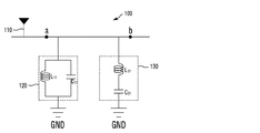
図1を参照すると、アンテナ装置100は、放射金属110、放射金属110と接地GNDとの間に連結され、周波数によってインピーダンス値が変更されるが、所定の周波数に応じて共振することにより放射金属110と接地GNDとの間が開放されるようにする第1インピーダンス部120、及び放射金属110と接地GNDとの間に連結され、周波数によってインピーダンス値が変更されるが、所定の周波数に応じて共振することにより放射金属110と接地GNDとの間が短絡されるようにする第2インピーダンス部130、を含んでもよい。
Referring to FIG. 1, an
アンテナ装置は、一つの放射金属110において、低域帯に属する信号と高域帯に属する信号とが共振することができる。また、アンテナ装置100は、二つの放射金属110において、それぞれ低域帯に属する信号と高域帯に属する信号とを送受信することができる。そして、放射金属110において低域帯周波数バンドに属する信号と高域帯周波数バンドに属する信号とが共振できるようにするために、放射金属110と接地GNDとの間に第1インピーダンス部120と第2インピーダンス部130とが並列に連結されてもよい。第1インピーダンス部120と第2インピーダンス部130はそれぞれ放射金属110に伝達される信号の周波数に応じてインピーダンス値が変更されてもよい。また、第1インピーダンス部120と第2インピーダンス部130はそれぞれ所定の周波数に応じて共振することができる。
The antenna device can resonate a signal belonging to the low band and a signal belonging to the high band in one
放射金属110で所定の周波数を有する信号が送受信されるとき、第1インピーダンス部120と第2インピーダンス部130はそれぞれ所定の周波数に応じて共振することができる。第1インピーダンス部120において送受信される信号が共振すると、第1インピーダンス部120のインピーダンスが無限大になり、第2インピーダンス部130において送受信される信号が共振すると、第2インピーダンス部130のインピーダンスは0になってもよい。第1インピーダンス部120のインピーダンスが無限大になり、第2インピーダンス部130のインピーダンスが0になると、アンテナ装置100は、図2aに示されているように、放射金属110は接地GNDに連結されてもよい。したがって、放射金属110に送受信される信号は接地GNDに伝達されるようになり、アンテナ装置100と連結されている外部装置(図示せず)に信号が伝達されないようになってもよい。
When a signal having a predetermined frequency is transmitted and received by the radiating
そして、放射金属110に所定の周波数より周波数が高い高域帯に属する信号が送受信されると、アンテナ装置100は図2bに示されているように、第1インピーダンス部120はキャパシタ成分CH1を有してもよく、第2インピーダンス部130はインダクタ成分LH1を有してもよい。放射金属110に送受信される高域帯信号のうち特定の高域帯信号は、第1インピーダンス部120のキャパシタ成分CH1と第2インピーダンス部130のインダクタ成分LH1とによって共振することができる。
When a signal belonging to a high band whose frequency is higher than a predetermined frequency is transmitted / received to / from the radiating
また、放射金属に所定の周波数より周波数が低い低域帯に属する信号が送受信されるとき、アンテナ装置100は、図2cに示されているように、第1インピーダンス部120はインダクタ成分LL1を有してもよく、第2インピーダンス部130はキャパシタ成分CL1を有してもよい。放射金属110に送受信される低域帯信号のうち特定の低域帯信号は、第1インピーダンス部120のインダクタ成分LL1と第2インピーダンス部130のキャパシタ成分CL1とによって共振することができる。
In addition, when a signal belonging to a low band whose frequency is lower than a predetermined frequency is transmitted / received to / from the radiating metal, the
第1インピーダンス部120と第2インピーダンス部130は、放射金属110に送受信される信号に応じてそれぞれインピーダンス成分の値が変更されてもよい。したがって、放射金属110に高域帯に属する信号が送受信される時に第1インピーダンス部120と第2インピーダンス部130とが有するインピーダンス値と、低域帯に属する信号が放射金属110に送受信される時に第1インピーダンス部120と第2インピーダンス部130とが有するインピーダンス値とは、異なってもよい。第1インピーダンス部120と第2インピーダンス部130の数は一つずつ示されているが、これに限定される訳ではなく、第1インピーダンス部120の数と第2インピーダンス部130はそれぞれ複数個が備えられてもよい。
In the
そして、第1インピーダンス部120と第2インピーダンス部130のインピーダンス成分の値が放射金属110に送受信される周波数によって変更されてもよいため、第1インピーダンス部120と第2インピーダンス部130によって放射金属110に高域帯に属する信号が送受信される時に共振されてもよく、低域帯に属する信号が送受信される時も共振されてもよい。一例として、放射金属110において共振する低域帯信号は850MHzを有する信号であってもよく、高域帯信号は1850MHz帯の信号であってもよい。また、所定の周波数は、低域帯信号の周波数と高域帯の周波数の平均周波数を用いることができる。しかし、これに限定される訳ではなく、低域帯信号の周波数と高域帯信号の周波数の平均に近い周波数を用いることが可能である。例えば、低域帯信号の周波数が850MHzであり、高域帯信号の周波数が1850MHzであれば、所定の周波数は1250MHzであってもよい。
Since the values of the impedance components of the
一実施形態において、第1インピーダンス部120はインダクタL11とキャパシタC11が並列に連結されており、第2インピーダンス部130は、インダクタL21とキャパシタC21が直列に連結されている。
In one embodiment,
したがって、アンテナ装置100は、高域帯信号に応じて共振することができ、低域帯信号に応じて共振することができ、高周波信号と低周波信号を広帯域化することができる。
Therefore, the
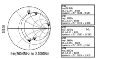
図3a及び図3bは、図1に示されたアンテナ装置に伝達される任意の信号の周波数に対する整合特性を表わす図面であり、図4aは図3aに対応するスミスチャートを表わし、図4bは、図3bに対応するスミスチャートを表わす。図3aは、放射金属のa地点で信号の周波数に対する整合特性を表わし、図3bは、放射金属のb地点で信号の周波数に対する整合特性を表わす。 3a and 3b are diagrams showing matching characteristics with respect to the frequency of an arbitrary signal transmitted to the antenna apparatus shown in FIG. 1, FIG. 4a is a Smith chart corresponding to FIG. 3a, and FIG. 3 represents a Smith chart corresponding to FIG. FIG. 3a shows the matching characteristic with respect to the frequency of the signal at the point a of the radiating metal, and FIG. 3b shows the matching characteristic with respect to the frequency of the signal at the point b of the radiating metal.
図1に示された放射金属110に、700MHzから2300MHzの間の周波数を有する信号が送受信されるとき、図1のa地点(a)において周波数と整合特性は、図3aに示されているように表わされてもよい。また、スミスチャートは図4aに示されているように表わされる。すなわち、放射金属110に850MHz程度の周波数を有する信号が伝達される時と、放射金属110に1850MHz程度の信号が伝達されるとき、それぞれ一つのポール(Pole)が形成されることが分かる。したがって、放射金属110に850MHz程度の周波数を有する信号と1850MHz程度の周波数を有する信号とが送受信されるとき、伝送損失が最も少なく発生し得ることが分かる。そして、周波数が1250MHzであれば、整合が成されないことが分かる。そして、図1のb地点(b)において周波数と利得関係は、図3bに示されているように表わされてもよい。また、スミスチャートは図4bに示されているように表わされる。図3bと図4を用いて周波数と利得を詳しくみてみると、放射金属110に約790MHz〜980MHz程度の周波数を有する信号が伝達される時と放射金属110に1700MHz〜2100MHz程度の信号が伝達される時、それぞれ2つのポール(Pole)が形成されることが分かる。すなわち、第1インピーダンス部120と第2インピーダンス部130によって低域帯周波数と高域帯周波数においてそれぞれ2つのポールが発生され得るようになる。これにより、伝送損失が少ない周波数範囲が広くなり、広帯域化して信号を送受信することができる。そして、周波数が1250MHzであれば、放射金属に送受信される信号が接地に伝達されて整合が成されないことが分かる。
When a signal having a frequency between 700 MHz and 2300 MHz is transmitted / received to / from the radiating
図5は、本発明によるアンテナ装置の他の一実施形態を示す回路図である。図6aないし図6cは、図5に示されたアンテナ装置に伝達される信号による等価回路図である。図6aは、放射金属に所定の周波数を有する信号が伝達される時のアンテナ装置の等価回路図であり、図6bは、放射金属に所定の周波数より高い周波数を有する信号が伝達される時のアンテナ装置の等価回路図であり、図6cは、放射金属に所定の周波数より低い周波数を有する信号が伝達される時のアンテナ装置の等価回路図である。 FIG. 5 is a circuit diagram showing another embodiment of the antenna device according to the present invention. 6a to 6c are equivalent circuit diagrams of signals transmitted to the antenna apparatus shown in FIG. FIG. 6A is an equivalent circuit diagram of the antenna device when a signal having a predetermined frequency is transmitted to the radiating metal, and FIG. 6B is a diagram when a signal having a frequency higher than the predetermined frequency is transmitted to the radiating metal. FIG. 6C is an equivalent circuit diagram of the antenna device when a signal having a frequency lower than a predetermined frequency is transmitted to the radiating metal.
図5を参照すると、アンテナ装置200は、放射金属210と、放射金属210と接地GNDとの間に連結され、周波数によってインピーダンス値が変更されるが、所定の周波数に応じて共振することにより放射金属210と接地GNDとの間が開放されるようにする第1インピーダンス部220と、放射金属210と接地GNDの間に連結され、周波数によってインピーダンス値が変更されるが、所定の周波数に応じて共振されることにより放射金属210と接地GNDとの間が短絡されるようにする第2インピーダンス部230と、放射金属210に直列に連結され、所定の周波数に応じて開放される第3インピーダンス部240と、所定の周波数に応じて短絡される第4インピーダンス部250とを含んでもよい。
Referring to FIG. 5, the
図5に示されたアンテナ装置200は、放射金属210に直列に連結されている第3インピーダンス部240と第4インピーダンス部250とをさらに含むことが、図1に示されたアンテナ装置100と異なる相違点である。ここでは、図1に示されたアンテナ装置100と異なる相違点に対してのみ説明する。
The
そして、放射金属210に所定の周波数を有する信号が送受信されると、第3インピーダンス部240は共振によってインピーダンスが無限大になり、第4インピーダンス部250は共振によってインピーダンスが0になることによって、アンテナ装置200は図6aのように示されてもよい。すなわち、第3インピーダンス部240によって放射金属210が途切れているのと同様になってもよい。したがって、第2インピーダンス部230によって放射金属210が接地GNDと連結されるようにし、第3インピーダンス部240によって放射金属210が外部機器(図示せず)と途切れている状態となるため、放射金属210には信号が送受信されず、アンテナ装置200と連結されている外部機器へ放射金属210に送受信される信号は送受信されなくてもよい。
When a signal having a predetermined frequency is transmitted / received to / from the radiating
そして、放射金属210に所定の周波数より周波数が高い高域帯に属する信号が送受信されると、第1インピーダンス部220と第3インピーダンス部240はそれぞれキャパシタ成分CH2、CH3を有してもよく、第2インピーダンス部230と第4インピーダンス部250はそれぞれインダクタ成分LH2、LH3を有してもよく、アンテナ装置100は図6bのように示されてもよい。したがって、第3インピーダンス部240と第4インピーダンス部250は、放射金属210に直列に連結されてもよい。そして、放射金属210に直列に連結されている第3インピーダンス部240のキャパシタ成分CH3と第4インピーダンス部250のインダクタ成分LH3によって放射金属210に送受信される高域帯信号は共振するようになり、放射金属210に送受信される高域帯信号は第3インピーダンス部240と第4インピーダンス部250とをバイパスすることができる。
When a signal belonging to a high frequency band having a frequency higher than a predetermined frequency is transmitted / received to / from the radiating
また、放射金属210に所定の周波数より周波数が低い低域帯に属する信号が送受信されると、第1インピーダンス部220と第3インピーダンス部240はインダクタ成分を有してもよく、第2インピーダンス部230と第4インピーダンス部250はキャパシタ成分を有してもよく、アンテナ装置200は図6cのように示されてもよい。第3インピーダンス部240と第4インピーダンス部250は放射金属210に直列に連結されてもよい。そして、放射金属210に直列に連結されている第3インピーダンス部240のインダクタ成分LL3と第4インピーダンス部250のキャパシタ成分CL3によって放射金属210に送受信される低域帯信号は共振することになり、放射金属210に送受信される低域帯信号は第3インピーダンス部240と第4インピーダンス部250とをバイパスすることができる。第3インピーダンス部240と第4インピーダンス部250の数は一つずつ示されているが、これに限定される訳ではなく、第3インピーダンス部240と第4インピーダンス部250の数はそれぞれ複数個が備えられてもよい。
In addition, when a signal belonging to a low band whose frequency is lower than a predetermined frequency is transmitted / received to / from the radiating
一実施形態において、第3インピーダンス部240はインダクタL31とキャパシタC31とが並列に連結されており、第4インピーダンス部250はインダクタL41とキャパシタC41とが直列に連結されてもよい。また、低域帯信号は850MHzを有する信号であってもよく、高域帯信号は1850MHz帯の信号であってもよい。また、所定の周波数は1250MHzであってもよい。
In one embodiment, the
したがって、アンテナ装置200は、高域帯信号に応じて共振することができ、低域帯信号に応じて共振することができて、高周波信号と低周波信号を広帯域化することができる。
Therefore, the
上記の説明において、第1インピーダンス部220、第2インピーダンス部230、第3インピーダンス部240、及び第4インピーダンス部250がすべて放射金属210に連結されていることが示されているが、これに限定される訳ではなく、第1インピーダンス部220と第2インピーダンス部230のみ放射金属210に連結されてもよく、第3インピーダンス部240と第4インピーダンス部250のみ放射金属210に連結されてもよい。
In the above description, it is shown that the
図7は、図5に示されたアンテナ装置に伝達される任意の信号の周波数に対する整合特性を表わす図面であり、図8は、図7に対応するスミスチャートを表わす。 FIG. 7 is a diagram showing a matching characteristic with respect to a frequency of an arbitrary signal transmitted to the antenna apparatus shown in FIG. 5, and FIG. 8 is a Smith chart corresponding to FIG.
図7及び図8を参照すると、図5に示された放射金属210に700MHzから2300MHzの間の周波数を有する信号が送受信されると、c地点(c)において周波数と利得の関係は図7に示されているように表わすことができる。また、スミスチャートは、図8に示されているように表わされる。放射金属210に850MHz程度の周波数を有する信号が送受信される時と放射金属210に1850MHz程度の信号が送受信される時、それぞれポール(Pole)が形成されることが分かる。一つのポールにおいて、伝送損失を最小化できる周波数の範囲が非常に広くなって、放射金属110に送受信される信号の伝送損失を最小化できる周波数の範囲が非常に広くなり得るようになる。したがって、広帯域化が成されたことが分かる。そして、周波数が1250MHzであれば、信号が接地に伝達されて整合が成されないことが分かる。
Referring to FIGS. 7 and 8, when a signal having a frequency between 700 MHz and 2300 MHz is transmitted to and received from the radiating
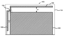
図9は、本発明によるアンテナ装置の構造を示す構造図である。 FIG. 9 is a structural diagram showing the structure of the antenna device according to the present invention.
図9を参照すると、アンテナ装置1000は、基板1100上に電極1200が形成されて接地として使用されてもよい。そして、基板1100上において一つの方向に第1放射金属1300が形成され、第1放射金属1300が形成された方向と垂直の方向に第2放射金属1400が形成されてもよい。第1放射金属1300が第2放射金属1400より長さがさらに長くてもよい。第1放射金属1300、第2放射金属1400、及び電極1100は、フィード(feed)1500に連結されてもよい。第1放射金属1300は低域帯周波数を有する信号が送受信されてもよく、第2放射金属1400は高域帯周波数を有する信号が送受信されてもよい。低域帯周波数を有する信号の周波数は850MHzであってもよく、高域帯周波数を有する信号の周波数は1850MHzであってもよい。また、第1放射金属1300と電極1200との間の間隔d1は8mmであってもよく、第2放射金属1400と電極1200との間の間隔d2は3mmであってもよい。
Referring to FIG. 9, the
また、ここで、アンテナ装置を平板逆Lアンテナを基準に説明したが、アンテナ装置がここに限定される訳ではない。 Here, the antenna device has been described based on the flat inverted L antenna, but the antenna device is not limited to this.
以上において、実施形態に説明された特徴、構造、効果などは、本発明の一つの実施形態に含まれ、必ずしも一つの実施形態にのみ限定される訳ではない。さらに、各実施形態において例示された特徴、構造、効果などは、実施形態が属する分野における通常の知識を有する者によって、他の実施形態についても組み合わせ又は併合されて実施可能である。したがって、このような組み合わせと変形に係る内容は、本発明の範囲に含まれるものと解釈されるべきである。 In the above, the features, structures, effects, and the like described in the embodiments are included in one embodiment of the present invention, and are not necessarily limited to only one embodiment. Furthermore, the features, structures, effects, and the like exemplified in each embodiment can be implemented by combining or merging other embodiments with those having ordinary knowledge in the field to which the embodiment belongs. Therefore, the contents relating to such combinations and modifications should be construed as being included in the scope of the present invention.
また、以上において実施形態を中心に説明したが、これは単に例示にすぎず、本発明を限定する訳ではなく、本発明が属する分野における通常の知識を有する者であれば、本実施形態の本質的な特徴を外れない範囲で、以上において例示されない様々な変形と応用が可能であることが分かるはずである。例えば、実施形態に具体的に示された各構成要素は、変形して実施することができる。そして、このような変形と応用に係る相違点は、添付の特許請求の範囲において規定する本発明の範囲に含まれるものと解釈されるべきである。 Although the embodiment has been mainly described above, this is merely an example, and does not limit the present invention. Any person having ordinary knowledge in the field to which the present invention belongs can be used. It should be understood that various modifications and applications not exemplified above are possible without departing from the essential characteristics. For example, each component specifically shown in the embodiment can be implemented by being modified. Such differences in modification and application should be construed as being included in the scope of the present invention as defined in the appended claims.
100 アンテナ装置
110 放射金属
120 第1インピーダンス部
130 第2インピーダンス部
GND 接地
DESCRIPTION OF
Claims (18)
前記放射金属と接地との間に連結され、周波数によってインピーダンス値が変更されるが、所定の周波数に応じて共振することにより前記放射金属と前記接地との間が開放されるようにする第1インピーダンス部と、
前記放射金属と前記接地との間に連結され、周波数によってインピーダンス値が変更されるが、前記所定の周波数に応じて共振することにより前記放射金属と前記接地との間が短絡されるようにする第2インピーダンス部と、
を含むアンテナ装置。 Radiation metal,
A first impedance is connected between the radiating metal and the ground, and an impedance value is changed according to a frequency, and the first radiating metal and the ground are opened by resonating according to a predetermined frequency. An impedance section;
It is connected between the radiating metal and the ground, and the impedance value is changed according to the frequency. However, the radiating metal and the ground are short-circuited by resonating according to the predetermined frequency. A second impedance part;
An antenna device including:
一端が前記放射金属に連結される第3インピーダンス部と、
一端が前記第3インピーダンス部に連結される第4インピーダンス部と、
を含むが、
前記第3インピーダンス部は、所定の周波数に応じて開放され、前記第4インピーダンス部は、前記所定の周波数に応じて短絡する、アンテナ装置。 Radiation metal,
A third impedance part having one end connected to the radiating metal;
A fourth impedance part having one end connected to the third impedance part;
Including
The antenna device, wherein the third impedance unit is opened according to a predetermined frequency, and the fourth impedance unit is short-circuited according to the predetermined frequency.
前記放射金属と前記接地との間に連結され、周波数によってインピーダンス値が変更されるが、前記所定の周波数に応じて共振することにより前記放射金属と前記接地との間が短絡されるようにする第2インピーダンス部と、
を含む、請求項12に記載のアンテナ装置。 A first impedance is connected between the radiating metal and the ground, and an impedance value is changed according to a frequency, and the first radiating metal and the ground are opened by resonating according to a predetermined frequency. An impedance section;
It is connected between the radiating metal and the ground, and the impedance value is changed according to the frequency. However, the radiating metal and the ground are short-circuited by resonating according to the predetermined frequency. A second impedance part;
The antenna device according to claim 12, comprising:
The radiant metal includes a first radiant metal that resonates in response to a signal in a low frequency band lower than the predetermined frequency, and a second radiant metal that resonates in response to a signal in a high frequency band higher than the predetermined frequency. The antenna device according to claim 12, comprising:
Applications Claiming Priority (2)
| Application Number | Priority Date | Filing Date | Title |
|---|---|---|---|
| KR1020130128212A KR101719551B1 (en) | 2013-10-28 | 2013-10-28 | Antenna apparatus |
| KR10-2013-0128212 | 2013-10-28 |
Related Child Applications (1)
| Application Number | Title | Priority Date | Filing Date |
|---|---|---|---|
| JP2016227746A Division JP2017046360A (en) | 2013-10-28 | 2016-11-24 | Antenna device |
Publications (1)
| Publication Number | Publication Date |
|---|---|
| JP2015089129A true JP2015089129A (en) | 2015-05-07 |
Family
ID=51830223
Family Applications (2)
| Application Number | Title | Priority Date | Filing Date |
|---|---|---|---|
| JP2014218803A Pending JP2015089129A (en) | 2013-10-28 | 2014-10-28 | Antenna device |
| JP2016227746A Pending JP2017046360A (en) | 2013-10-28 | 2016-11-24 | Antenna device |
Family Applications After (1)
| Application Number | Title | Priority Date | Filing Date |
|---|---|---|---|
| JP2016227746A Pending JP2017046360A (en) | 2013-10-28 | 2016-11-24 | Antenna device |
Country Status (5)
| Country | Link |
|---|---|
| US (1) | US10074903B2 (en) |
| EP (1) | EP2866300A1 (en) |
| JP (2) | JP2015089129A (en) |
| KR (1) | KR101719551B1 (en) |
| CN (1) | CN104577359A (en) |
Families Citing this family (10)
| Publication number | Priority date | Publication date | Assignee | Title |
|---|---|---|---|---|
| US10034092B1 (en) | 2016-09-22 | 2018-07-24 | Apple Inc. | Spatial headphone transparency |
| CN109546310B (en) * | 2018-12-12 | 2021-01-08 | 维沃移动通信有限公司 | Antenna structure and communication terminal |
| KR102501647B1 (en) * | 2019-01-10 | 2023-02-20 | 삼성전자 주식회사 | A mixer for reducing a local frequency signal generated at output of the mixer |
| CN110380189A (en) * | 2019-07-23 | 2019-10-25 | 广东以诺通讯有限公司 | A kind of miniature antenna and terminal |
| JP7356000B2 (en) * | 2019-08-14 | 2023-10-04 | ミツミ電機株式会社 | antenna device |
| US11361745B2 (en) | 2019-09-27 | 2022-06-14 | Apple Inc. | Headphone acoustic noise cancellation and speaker protection |
| US11166099B2 (en) | 2019-09-27 | 2021-11-02 | Apple Inc. | Headphone acoustic noise cancellation and speaker protection or dynamic user experience processing |
| US11206004B1 (en) * | 2020-09-16 | 2021-12-21 | Apple Inc. | Automatic equalization for consistent headphone playback |
| CN112583373B (en) * | 2020-12-08 | 2023-09-12 | 北京邮电大学 | Band-pass filter chip with frequency-dependent complex source and load |
| US11688383B2 (en) | 2021-08-27 | 2023-06-27 | Apple Inc. | Context aware compressor for headphone audio feedback path |
Citations (7)
| Publication number | Priority date | Publication date | Assignee | Title |
|---|---|---|---|---|
| JPH04233303A (en) * | 1990-12-28 | 1992-08-21 | Matsushita Electric Ind Co Ltd | Antenna device |
| JP2000036721A (en) * | 1998-05-12 | 2000-02-02 | Nec Corp | Method and circuit for impedance matching |
| US20020180534A1 (en) * | 2001-03-09 | 2002-12-05 | Florian Bohn | Switchless multi-resonant, multi-band power amplifier |
| WO2004036687A1 (en) * | 2002-10-15 | 2004-04-29 | Hitachi, Ltd. | Small multimode antenna and high frequency module using it |
| JP2004242269A (en) * | 2002-12-12 | 2004-08-26 | Mitsubishi Electric Corp | Two-frequency matching circuit |
| JP2008054174A (en) * | 2006-08-28 | 2008-03-06 | Mitsubishi Electric Corp | 90-degree hybrid circuit |
| WO2009028201A1 (en) * | 2007-08-29 | 2009-03-05 | Panasonic Corporation | Double channel matching circuit |
Family Cites Families (7)
| Publication number | Priority date | Publication date | Assignee | Title |
|---|---|---|---|---|
| JP2003249811A (en) | 2001-12-20 | 2003-09-05 | Murata Mfg Co Ltd | Double-resonance antenna apparatus |
| KR100782301B1 (en) * | 2006-09-21 | 2007-12-06 | 주식회사 이엠따블유안테나 | Antenna with adjustable resonant frequency using metamaterial and device comprising the same |
| KR100784411B1 (en) * | 2006-11-29 | 2007-12-11 | 전자부품연구원 | Front-end module for dual-band terminal |
| JP2009278192A (en) * | 2008-05-12 | 2009-11-26 | Sony Ericsson Mobilecommunications Japan Inc | Antenna device and communication terminal |
| KR101211870B1 (en) * | 2010-06-28 | 2012-12-13 | 박혜식 | The bamboo plywood |
| KR101217468B1 (en) * | 2010-11-03 | 2013-01-02 | 주식회사 네오펄스 | Inverted F Antenna With Parastic Coupling Resonance |
| CN202487756U (en) * | 2011-12-29 | 2012-10-10 | 惠州Tcl移动通信有限公司 | Mobile phone and double-frequency resonant antenna thereof |
-
2013
- 2013-10-28 KR KR1020130128212A patent/KR101719551B1/en active IP Right Grant
-
2014
- 2014-10-27 US US14/524,735 patent/US10074903B2/en active Active
- 2014-10-28 EP EP20140190614 patent/EP2866300A1/en not_active Withdrawn
- 2014-10-28 JP JP2014218803A patent/JP2015089129A/en active Pending
- 2014-10-28 CN CN201410588697.9A patent/CN104577359A/en active Pending
-
2016
- 2016-11-24 JP JP2016227746A patent/JP2017046360A/en active Pending
Patent Citations (7)
| Publication number | Priority date | Publication date | Assignee | Title |
|---|---|---|---|---|
| JPH04233303A (en) * | 1990-12-28 | 1992-08-21 | Matsushita Electric Ind Co Ltd | Antenna device |
| JP2000036721A (en) * | 1998-05-12 | 2000-02-02 | Nec Corp | Method and circuit for impedance matching |
| US20020180534A1 (en) * | 2001-03-09 | 2002-12-05 | Florian Bohn | Switchless multi-resonant, multi-band power amplifier |
| WO2004036687A1 (en) * | 2002-10-15 | 2004-04-29 | Hitachi, Ltd. | Small multimode antenna and high frequency module using it |
| JP2004242269A (en) * | 2002-12-12 | 2004-08-26 | Mitsubishi Electric Corp | Two-frequency matching circuit |
| JP2008054174A (en) * | 2006-08-28 | 2008-03-06 | Mitsubishi Electric Corp | 90-degree hybrid circuit |
| WO2009028201A1 (en) * | 2007-08-29 | 2009-03-05 | Panasonic Corporation | Double channel matching circuit |
Also Published As
| Publication number | Publication date |
|---|---|
| KR20150080931A (en) | 2015-07-13 |
| EP2866300A1 (en) | 2015-04-29 |
| JP2017046360A (en) | 2017-03-02 |
| US10074903B2 (en) | 2018-09-11 |
| US20150116167A1 (en) | 2015-04-30 |
| KR101719551B1 (en) | 2017-03-24 |
| CN104577359A (en) | 2015-04-29 |
Similar Documents
| Publication | Publication Date | Title |
|---|---|---|
| JP2017046360A (en) | Antenna device | |
| US9577332B2 (en) | Electronic device and multi-band antenna | |
| US9735471B2 (en) | Antenna structure and wireless communication device employing same | |
| US9680222B2 (en) | Antenna structure and wireless communication device using the same | |
| TWI628867B (en) | Antenna assembly and wireless communication device having the same | |
| US9401543B2 (en) | Broadband antenna | |
| US9614571B2 (en) | Multi-band isolator assembly | |
| AU2015244191B2 (en) | Capacitively-coupled isolator assembly | |
| US9660342B2 (en) | Antenna structure and wireless communication device employing same | |
| US20130234911A1 (en) | Mobile communication terminal with improved isolation | |
| US10615486B2 (en) | Antenna system | |
| KR20200039810A (en) | Antenna device and terminal | |
| CN104752827B (en) | A kind of double-feed antenna system and electronic equipment | |
| US20160204520A1 (en) | Multi-band antenna with a tuned parasitic element | |
| US10230157B2 (en) | WIFI and GPS antenna | |
| US20150214995A1 (en) | Semiconductor device, and transmission and reception circuit | |
| US20150109169A1 (en) | Wireless communication device | |
| US9306281B2 (en) | Wireless communication device | |
| JP2018198372A (en) | Electronic apparatus | |
| TW201935758A (en) | Antenna structure and wireless communication device with same | |
| KR101245731B1 (en) | Multiband antenna | |
| WO2011110216A1 (en) | An antenna device adapted for simultaneous reception of a first frequency band and a second frequency band |
Legal Events
| Date | Code | Title | Description |
|---|---|---|---|
| A977 | Report on retrieval |
Free format text: JAPANESE INTERMEDIATE CODE: A971007 Effective date: 20151112 |
|
| A131 | Notification of reasons for refusal |
Free format text: JAPANESE INTERMEDIATE CODE: A131 Effective date: 20151124 |
|
| A521 | Request for written amendment filed |
Free format text: JAPANESE INTERMEDIATE CODE: A523 Effective date: 20160223 |
|
| A02 | Decision of refusal |
Free format text: JAPANESE INTERMEDIATE CODE: A02 Effective date: 20160726 |
|
| A521 | Request for written amendment filed |
Free format text: JAPANESE INTERMEDIATE CODE: A523 Effective date: 20161124 |
|
| A521 | Request for written amendment filed |
Free format text: JAPANESE INTERMEDIATE CODE: A523 Effective date: 20161229 |
|
| A911 | Transfer to examiner for re-examination before appeal (zenchi) |
Free format text: JAPANESE INTERMEDIATE CODE: A911 Effective date: 20170105 |
|
| A912 | Re-examination (zenchi) completed and case transferred to appeal board |
Free format text: JAPANESE INTERMEDIATE CODE: A912 Effective date: 20170303 |