JP2015038798A - Magnetic recording apparatus and method of manufacturing the same - Google Patents
Magnetic recording apparatus and method of manufacturing the same Download PDFInfo
- Publication number
- JP2015038798A JP2015038798A JP2014165195A JP2014165195A JP2015038798A JP 2015038798 A JP2015038798 A JP 2015038798A JP 2014165195 A JP2014165195 A JP 2014165195A JP 2014165195 A JP2014165195 A JP 2014165195A JP 2015038798 A JP2015038798 A JP 2015038798A
- Authority
- JP
- Japan
- Prior art keywords
- slider
- waveguide
- protrusion
- light source
- optical path
- Prior art date
- Legal status (The legal status is an assumption and is not a legal conclusion. Google has not performed a legal analysis and makes no representation as to the accuracy of the status listed.)
- Pending
Links
Images


Classifications
-
- G—PHYSICS
- G11—INFORMATION STORAGE
- G11B—INFORMATION STORAGE BASED ON RELATIVE MOVEMENT BETWEEN RECORD CARRIER AND TRANSDUCER
- G11B5/00—Recording by magnetisation or demagnetisation of a record carrier; Reproducing by magnetic means; Record carriers therefor
- G11B5/127—Structure or manufacture of heads, e.g. inductive
- G11B5/31—Structure or manufacture of heads, e.g. inductive using thin films
- G11B5/3163—Fabrication methods or processes specially adapted for a particular head structure, e.g. using base layers for electroplating, using functional layers for masking, using energy or particle beams for shaping the structure or modifying the properties of the basic layers
- G11B5/3173—Batch fabrication, i.e. producing a plurality of head structures in one batch
-
- G—PHYSICS
- G11—INFORMATION STORAGE
- G11B—INFORMATION STORAGE BASED ON RELATIVE MOVEMENT BETWEEN RECORD CARRIER AND TRANSDUCER
- G11B5/00—Recording by magnetisation or demagnetisation of a record carrier; Reproducing by magnetic means; Record carriers therefor
- G11B5/127—Structure or manufacture of heads, e.g. inductive
- G11B5/31—Structure or manufacture of heads, e.g. inductive using thin films
- G11B5/3109—Details
- G11B5/313—Disposition of layers
- G11B5/3133—Disposition of layers including layers not usually being a part of the electromagnetic transducer structure and providing additional features, e.g. for improving heat radiation, reduction of power dissipation, adaptations for measurement or indication of gap depth or other properties of the structure
- G11B5/314—Disposition of layers including layers not usually being a part of the electromagnetic transducer structure and providing additional features, e.g. for improving heat radiation, reduction of power dissipation, adaptations for measurement or indication of gap depth or other properties of the structure where the layers are extra layers normally not provided in the transducing structure, e.g. optical layers
-
- G—PHYSICS
- G11—INFORMATION STORAGE
- G11B—INFORMATION STORAGE BASED ON RELATIVE MOVEMENT BETWEEN RECORD CARRIER AND TRANSDUCER
- G11B5/00—Recording by magnetisation or demagnetisation of a record carrier; Reproducing by magnetic means; Record carriers therefor
- G11B5/48—Disposition or mounting of heads or head supports relative to record carriers ; arrangements of heads, e.g. for scanning the record carrier to increase the relative speed
- G11B5/58—Disposition or mounting of heads or head supports relative to record carriers ; arrangements of heads, e.g. for scanning the record carrier to increase the relative speed with provision for moving the head for the purpose of maintaining alignment of the head relative to the record carrier during transducing operation, e.g. to compensate for surface irregularities of the latter or for track following
- G11B5/60—Fluid-dynamic spacing of heads from record-carriers
- G11B5/6005—Specially adapted for spacing from a rotating disc using a fluid cushion
- G11B5/6088—Optical waveguide in or on flying head
-
- G—PHYSICS
- G11—INFORMATION STORAGE
- G11B—INFORMATION STORAGE BASED ON RELATIVE MOVEMENT BETWEEN RECORD CARRIER AND TRANSDUCER
- G11B5/00—Recording by magnetisation or demagnetisation of a record carrier; Reproducing by magnetic means; Record carriers therefor
- G11B2005/0002—Special dispositions or recording techniques
- G11B2005/0005—Arrangements, methods or circuits
- G11B2005/0021—Thermally assisted recording using an auxiliary energy source for heating the recording layer locally to assist the magnetization reversal
Abstract
Description
発明の詳細な説明
概要
実施形態は、スライダと、スライダの外面上に配置された光源と、スライダの外面の上方に延びる突起とを含む装置に関する。光源は、スライダの外面に対して実質的に平行に整列された光共振器を含む。突起は、光源に光結合された光路変換素子を含む。
DETAILED DESCRIPTION OF THE INVENTION Overview Embodiments relate to an apparatus that includes a slider, a light source disposed on the outer surface of the slider, and a protrusion extending above the outer surface of the slider. The light source includes an optical resonator aligned substantially parallel to the outer surface of the slider. The protrusion includes an optical path conversion element optically coupled to the light source.
他の実施形態は、スライダと、スライダの外面の上方に延びる突起とを含む装置を製造する方法に関する。1つの方法は、複数の導波路要素をウェハ上にパターン堆積し、複数の導波路要素は、その突起中に光路変換素子を含むステップと、ウェハをスライスして、複数の導波路要素を含むスライダバーを製造するステップと、複数の導波路要素を含むスライダバーをダイシングして、ウェハ上に配置されたスライダ本体を製造するステップと、スライダ本体をパターンエッチングして、外面の上方に延びる突起を有するスライダバックパッドを製造し、突起は光路変換素子を含むステップとを含む。 Another embodiment relates to a method of manufacturing an apparatus that includes a slider and a protrusion that extends above the outer surface of the slider. One method pattern deposits a plurality of waveguide elements on a wafer, the plurality of waveguide elements including an optical path conversion element in its protrusion, and slicing the wafer to include a plurality of waveguide elements. A step of manufacturing a slider bar, a step of manufacturing a slider body disposed on the wafer by dicing the slider bar including a plurality of waveguide elements, and a protrusion extending above the outer surface by pattern etching the slider body. And a protrusion including an optical path conversion element.
上記の概要は、本開示の開示される各実施形態またはすべての実施例を記載することを意図するものではない。以下の図および詳細な説明は、より具体的に例示的な実施形態を例証する。 The above summary is not intended to describe each disclosed embodiment or every implementation of the present disclosure. The following figures and detailed description illustrate exemplary embodiments more specifically.
明細書全体を通して、添付の図面を参照し、図中、同一の参照番号は同一の要素を示す。 Throughout the specification, reference is made to the accompanying drawings, wherein like reference numerals designate like elements.
詳細な説明
図は必ずしも縮尺通りではない。図中に用いられる同一の番号は、同一の部品を指す。しかしながら、ある図中である部品を指すのにある番号を用いても、同じ番号で示される別の図中の当該部品を限定することを意図するものではないことが理解されるであろう。
Detailed description The figures are not necessarily drawn to scale. The same numbers used in the figures refer to the same parts. However, it will be understood that the use of a number to refer to a part in one figure is not intended to limit that part in another figure indicated by the same number.
以下の説明では、本願の記述の一部をなすとともにいくつかの特定の実施形態を例示する添付の図面のセットが参照される。他の実施形態が想定され、これらは本開示の範囲から逸脱することなく行われ得ることが理解されるべきである。したがって、以下の詳細な説明は、限定的な意味で捉えられるべきではない。 In the following description, reference is made to the accompanying set of drawings that form a part of this description and that illustrate some specific embodiments. It is to be understood that other embodiments are envisioned and can be made without departing from the scope of the present disclosure. The following detailed description is, therefore, not to be taken in a limiting sense.
特に記載がないかぎり、本明細書および請求項で用いられる特徴サイズ、量、および物性を表わす数字はすべて、すべての場合において「約」という用語により修飾されるものとして理解されるべきである。したがって、別段の記載がないかぎり、上記の明細書および添付の請求項に記載される数値パラメータは、本明細書中に開示される教示を利用して、当業者により得ようとされる所望の特性に応じて変化し得る近似値である。終点による数値範囲の使用は、その範囲内のすべての数字(たとえば、1〜5は、1、1.5、2、2.75、3、3.80、4、および5を含む)およびその範囲内の任意の範囲を含む。 Unless otherwise stated, all feature sizes, amounts, and physical numbers used in the specification and claims are to be understood as being modified by the term “about” in all cases. Accordingly, unless otherwise stated, the numerical parameters set forth in the above specification and the appended claims can be obtained as desired by one of ordinary skill in the art using the teachings disclosed herein It is an approximate value that can change according to the characteristics. The use of numerical ranges by endpoints means that all numbers within that range (eg 1 to 5 include 1, 1.5, 2, 2.75, 3, 3.80, 4, and 5) and Includes any range within the range.
ここに開示されるさまざまな実施形態は、概ね、磁気書込ヘッドの一部であり得る磁気書込装置へのレーザダイオードの結合を容易にする装置および装置の製造方法に関する。装置は、スライダと、スライダの外面上に配置された光源と、スライダの外面の上方に延びる突起とを含む。光源は、スライダの外面に対して実質的に平行に整列された光共振器を含む。突起は、光源に光結合された光路変換素子を有する。 The various embodiments disclosed herein relate generally to an apparatus and method of manufacturing an apparatus that facilitates coupling of a laser diode to a magnetic writing device that can be part of a magnetic write head. The apparatus includes a slider, a light source disposed on the outer surface of the slider, and a protrusion extending above the outer surface of the slider. The light source includes an optical resonator aligned substantially parallel to the outer surface of the slider. The protrusion has an optical path conversion element optically coupled to the light source.
本開示は概ね、ハードドライブなどの磁気記録デバイスに用いられる読取−書込ヘッドに関する。特に、本開示は、磁気媒体の面データ密度を増加させるために用いられ得る、熱アシスト型磁気記録(HAMR)に関する。HAMRデバイスでは、特殊な構成の磁気媒体において、情報ビットが高温で記憶層中に記録される。熱の使用は、さもなければ磁気媒体の面データ密度を限定するおそれがある超常磁性効果を克服することができる。このため、HAMRデバイスは、小さく限定された媒体部分(スポットサイズ)を加熱するために光子エネルギーを照射するレーザを含み得、同時に、磁気書込ヘッドは記録のために媒体に磁場を印加する。 The present disclosure relates generally to read-write heads used in magnetic recording devices such as hard drives. In particular, the present disclosure relates to thermally assisted magnetic recording (HAMR) that can be used to increase the surface data density of magnetic media. In HAMR devices, information bits are recorded in the storage layer at a high temperature in a specially configured magnetic medium. The use of heat can overcome the superparamagnetic effect that would otherwise limit the surface data density of magnetic media. For this reason, HAMR devices can include a laser that irradiates photon energy to heat a small, defined medium portion (spot size), while the magnetic write head applies a magnetic field to the medium for recording.
極めて小さく限定されたホットスポットを達成する1つの方法は、ハードドライブスライダの空気軸受表面近傍に配置されたプラズモン光アンテナまたはアパーチャなどの光近接場トランスデューサ(NFT)を使用することである。光は、光源(たとえばレーザダイオード)からスライダ内に集積された光学部品に照射され得る。このような集積された光学部品は、それぞれの屈折率間に高コントラストを有するコア層およびクラッド層から形成される導波路を含み得る。導波路中に伝搬する光は、平面型固浸ミラー(PSIM)などの集光要素に向けられてもよい。PSIMは、エネルギーをNFTに集中させてもよい。NFTによって、エネルギーが非常に小さなスポットで媒体に照射される。 One way to achieve a very small and limited hot spot is to use an optical near field transducer (NFT) such as a plasmon optical antenna or aperture located near the air bearing surface of the hard drive slider. Light can be applied from a light source (eg, a laser diode) to an optical component integrated in the slider. Such integrated optical components may include a waveguide formed from a core layer and a cladding layer that have a high contrast between their respective refractive indices. Light propagating in the waveguide may be directed to a light collection element such as a planar solid immersion mirror (PSIM). The PSIM may concentrate energy on the NFT. NFT irradiates the medium with a very small spot of energy.
導波路、NFT、およびPSIMは、スライダ内に形成され得る集積光デバイスである。集積光学部品の分野は一般的に、基板上に光学デバイスを構築することに関し、これらはときに電子部品と組み合わされて、機能的システムまたはサブシステムを生み出す。光は、層堆積技術を用いて基板上に堆積された導波路を介して部品間に伝達され得る。これらの導波路は、中間のコア層は比較的高い屈折率を有する材料の層として、上部/底部のクラッド層は比較的低い屈折率を有する材料の層として形成され得る。上述のNFTおよびPSIMを含む他の光学部品も同様に形成され得る。 Waveguides, NFTs, and PSIMs are integrated optical devices that can be formed in a slider. The field of integrated optics generally relates to building optical devices on a substrate, which are sometimes combined with electronic components to create a functional system or subsystem. Light can be transmitted between the components via waveguides deposited on the substrate using layer deposition techniques. These waveguides may be formed as a layer of material having a relatively high refractive index in the middle core layer and a layer of material having a relatively low refractive index in the top / bottom cladding layer. Other optical components, including NFT and PSIM described above, can be similarly formed.
HAMRスライダでは、光はレーザダイオードなどの光源からこれらの集積光学部品内に照射される。光をスライダ内に照射する1つの方法は、外部に設置されたレーザからスライダ内に作られた光導波路またはグレーティング結合器を介して光をスライダ内に照射することである。光源からの光は、磁気記録媒体中の小さな体積を急速に加熱してその保磁力を低下させるのに十分な出力を有する必要がある。これにより、媒体が冷却されてその保磁力を増加させ、磁化を封じ込める前に、発生された磁場は、小さな体積において磁気媒体を磁場に整列させるようにすることができる。たとえばレーザダイオードにおけるレーザ出力は、レーザの光学システムの光共振器の長さと相互に関連し得る。レーザをスライダの方向に向ける1つの方法は、添付の図面に図示するように、レーザの光共振器をスライダの外面に沿って整列させることである。添付の図面は、スライダの外面に対して実質的に平行に整列させられたスライダを図示する。 In a HAMR slider, light is emitted into these integrated optical components from a light source such as a laser diode. One method of irradiating light into the slider is to irradiate light into the slider from an externally installed laser through an optical waveguide or grating coupler made in the slider. The light from the light source must have sufficient power to rapidly heat a small volume in the magnetic recording medium and reduce its coercivity. This allows the generated magnetic field to align the magnetic medium with the magnetic field in a small volume before the medium is cooled to increase its coercivity and contain the magnetization. For example, the laser power in a laser diode can be correlated to the length of the optical resonator of the laser's optical system. One way to direct the laser toward the slider is to align the laser's optical resonator along the outer surface of the slider, as illustrated in the accompanying drawings. The accompanying drawings illustrate a slider aligned substantially parallel to the outer surface of the slider.
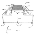
図1は、開示されるスライダを含むHAMR装置100の一実施形態の斜視図である。HAMR装置100はHAMRスライダ103を含む。レーザダイオード102などの光源は、HAMRスライダ103のトレーリィングエッジ表面104の近くのHAMRスライダ103の外面105上に位置する。レーザダイオード102は、HAMRスライダ103の空気軸受表面(「媒体側表面」とも呼ぶ)109上に一方のエッジを有する読取/書込ヘッド106の近くに光を照射する。媒体側表面109は、デバイス動作中に移動する媒体表面(図示せず)の近くに保持される。
FIG. 1 is a perspective view of one embodiment of a
レーザダイオード102は、読取/書込ヘッド106の近傍の点で媒体を加熱するために電磁エネルギーを供給する。導波路110などの光結合部品は、HAMRスライダ103内に一体的に形成され、レーザダイオード102から記録媒体に光を伝送する。特に、導波路110およびNFT112は、読取/書込ヘッド106近くに位置し、書込動作中に媒体を局所的に加熱してもよい。この例において、レーザダイオード102は端面発光デバイスであってもよいが、導波路110およびNFT112は、任意の光源および光伝送機構とともに用いられてもよいことが認識されるであろう。たとえば、端面発光レーザの代わりに面発光レーザ(SEL)を使用してもよい。
The
図1は、HAMRスライダ103の外面105上に配置されたレーザダイオード102を示す。レーザダイオード102は、図1に示されるように、スライダの外部に設置されてもよい。レーザダイオード102は、HAMRスライダ103の外面105に対して実質的に平行に整列された光共振器(図示せず)を含む。レーザダイオード102の光共振器から発される光は、レーザダイオード102から出て、外面105に対して実質的に平行な方向に沿って入力導波路122内に注入され得る。HAMR装置100は、HAMRスライダ103の外面105の上方に延びる突起107を含む。図1では、HAMRスライダ103の突起107は、HAMRスライダ103に一体化された部品であり、これは、HAMRスライダ103および突起107が、以下にさらに説明するように製造される一体的な構造(単一部品)からなることを意味する。HAMRスライダ103の突起107、入力導波路122、光路変換要素108、および入力導波路122は、レーザダイオード102の出力に光結合される。光路変換要素108は、入力導波路122からの光を導波路110内に方向変換させる。導波路110は、レーザダイオード102からのエネルギーを記録媒体に向けるように構成される。光路変換要素108は、湾曲導波路、ミラー、または、入力導波路122からの光を導波路110に方向変換させる任意の他の光学要素を含み得る。図1に図示する実施形態では、光はスライダの表面に対して実質的に垂直な方向に方向変換され、NFT112にエネルギーを供給するように光結合される。
FIG. 1 shows a
HAMRデバイスは、典型的な磁気媒体の面データ密度を限定する超常磁性効果を克服するために、上記のタイプの光学デバイスを利用して磁気記録媒体(たとえばハードディスク)を加熱する。HAMR媒体に書込む際、光は、書込が行なわれるトラック上の小さなホットスポット内に集束され得る。光は導波路110を通って伝搬し、導波路から直接または集光要素を介してNFT112に結合される。結合器、ミラー、プリズムなどの他の光学要素もスライダと一体的に形成されてもよい。HAMR記録ヘッドに用いられる光学要素は、一般的に集積光学デバイスと呼ばれる。
HAMR devices use the above type of optical device to heat a magnetic recording medium (eg, a hard disk) to overcome the superparamagnetic effect that limits the surface data density of typical magnetic media. When writing to a HAMR medium, the light can be focused into a small hot spot on the track where writing takes place. Light propagates through the
回折限界として知られるものの結果として、光学部品を用いて光の波長の約半分未満の寸法に集光させることができない。一部のHAMR設計で用いられるレーザは、700〜1550nmのオーダの波長を有する光を生じるが、所望のホットスポットは50nm以下のオーダである。したがって、望ましいホットスポットサイズは、光の波長の半分をゆうに下回る。光学的集光器を用いて望ましいホットスポットサイズを得ることは、回折がこのスケールで限界となるため不可能である。その結果、NFT112を使用して媒体上にホットスポットを作る。
As a result of what is known as the diffraction limit, optical components cannot be used to focus to dimensions less than about half the wavelength of light. While lasers used in some HAMR designs produce light having a wavelength on the order of 700-1550 nm, the desired hot spot is on the order of 50 nm or less. Thus, the desired hot spot size is well below half the wavelength of light. Obtaining the desired hot spot size using an optical concentrator is not possible because diffraction is limited at this scale. As a result,
NFT112は、意図される波長で局所的表面プラズモン共鳴に達するように設計された近接場光学デバイスである。導波路110および/または他の光学要素は、NFT112が位置するトランスデューサ領域(たとえば焦点)上に光を集束させる。NFT112は、この光の集束に応じて表面プラズモン共鳴を達成するように設計されている。共鳴点では、金属表面での電子の集団振動により、高電界がNFT112を囲む。この電界の一部が記憶媒体内を通り抜けて、吸収されることにより、記録されている媒体上のスポットの温度を上昇させる。一般的にNFTは、アルミニウム、金、銀、銅、またはこれらの合金などの表面プラズモン(「プラズモン金属」)を支持する材料からなる。NFTは他の材料を有してもよいが、それらの外面上に表面プラズモンを支持する材料を有する必要がある。
The
図2は、図1に図示するHAMR装置の一実施形態のより詳細な側面図である。HAMR装置200は、スライダ203と、スライダ203の外面205上に配置されたレーザダイオード202と、スライダ203の外面205の上方に延びる突起207とを含む。図2に示されるように、突起207はスライダ203と一体的であり、突起207を有する単一部品のスライダ203を形成し得る。レーザダイオード202は光共振器224を含み、この実施形態では、光共振器224は一方側に全反射ミラー223A、他方側に部分反射ミラー223Bを有する。光共振器224は外面205に沿って整列され、スライダ203の外面205に対して実質的に平行に整列されてもよい。レーザダイオード202から発される光は、突起207中の導波路210の入力導波路222内に照射される。光路変換要素209は、レーザダイオード202から入力導波路222内に照射される光を方向変換するように構成されている。たとえば、一部の実施形態では、光路変換要素は、図2に示されるように、入力光の方向を光共振器224に対して実質的に垂直な方向に変更してもよい。図2に示される実施形態では、導波路210および光路変換要素207は、突起207内に埋込まれ、以下により詳しく説明するように突起207と一体的となるように製造される。レーザダイオードは、リフローはんだバンプ230により、機械的に、熱的に、および/または電気的にスライダに結合され得る。スライダ203の上面205上に配置された少なくとも2つのはんだバンプ230は、少なくとも2つのはんだバンプのリフローに応じて、レーザダイオード202の出力光と導波路222の入力部との間の位置合わせを容易にする。
FIG. 2 is a more detailed side view of one embodiment of the HAMR device illustrated in FIG. The
図3および図4は、外面の上方に延びる突起を有する、開示されるスライダの2つの実施形態の斜視図である。図3は、外面305を有するスライダ300の例示である。スライダ300は、光源(図示せず)と、図示されるスライダ300の外面の上方に延びる突起307とを含む装置の一部である。図3では、突起307は、スライダ300の幅の実質的に中央に位置する。しかしながら、他の実施形態では、矢印308により示されるように、突起307はスライダ300の幅に沿って(図3中のy−軸に沿って)任意の場所に位置し得る。はんだバンプ330は、これらの一部が電気配線335に取付けられており、レーザダイオード(図示せず)と電気的、熱的、および/または機械的に連通している。少なくとも2つのはんだバンプ330を用いて、鉛直方向(図3中z−軸に沿って)、水平方向(図3中x−軸に沿って)、またはこれらの方向の組合せにおいて、スライダ表面305にレーザダイオードをセルフアライメントさせることができる。レーザダイオードは、光路変換要素(さまざまな実施形態では、導波路またはミラー中に湾曲部を含んでもよい)がレーザダイオードに光結合されるようにアライメントされる。
3 and 4 are perspective views of two embodiments of the disclosed slider having protrusions extending above the outer surface. FIG. 3 is an illustration of a
図4は、外面405を有するスライダ400の例示である。スライダ400は、光源(図示せず)と、図示されるスライダ400の外面の上方に延びる突起407とを含む装置の一部である。図4では、突起407は、スライダ400のエッジ側に位置する。はんだバンプ430は、その一部が電気配線435に取付けられており、レーザダイオード(図示せず)と電気的、熱的、および/または機械的に連通している。少なくとも2つのはんだバンプ430を用いて、レーザをスライダ表面405にセルフアライメントさせることができる。
FIG. 4 is an illustration of a
いくつかの実施形態では、装置の突起は、スライダの実質的に中心に位置し得る。他の実施形態では、装置の突起は、スライダの実質的に中心でなく、スライダの幅に沿った任意の場所に位置し得る。いくつかの他の実施形態では、突起は、スライダのほぼ全幅にわたって延びてもよい。一般的に、スライダの外面の上方に延びる突起の位置または形状に限定はない。突起の形状は、図3および図4に示されるように立方体の角部を含み得、または、他の実施形態では、丸まった角部もしくは任意の他の形状を有し得る。開示される突起は、スライダの外面の上方に延び得、光源に光結合された光路変換要素を含み得る。 In some embodiments, the protrusion of the device may be located substantially in the center of the slider. In other embodiments, the protrusions of the device may be located anywhere along the width of the slider rather than substantially the center of the slider. In some other embodiments, the protrusions may extend over substantially the entire width of the slider. In general, there is no limitation on the position or shape of the protrusion extending above the outer surface of the slider. The shape of the protrusions may include cubic corners as shown in FIGS. 3 and 4, or in other embodiments may have rounded corners or any other shape. The disclosed protrusion may extend above the outer surface of the slider and may include a light path changing element that is optically coupled to the light source.
図5は、開示される装置の別の実施形態の斜視図である。図5は、装置500の一部であるスライダ表面(バックパッド505とも呼ぶ)を有するスライダ504を図示する。レーザダイオード502は、装置500から取外されており、はんだバンプの位置が見えている。装置500は、スライダの外面の少なくとも一部を形成するスライダバックパッド505を有するスライダ504を含む。突起507は、スライダバックパッド505上に配置される。いくつかの実施形態では、突起507は、スライダ504および突起507が一体化された構造を形成するように、スライダ504の一体的な部品である。レーザダイオード502(突起507とスライダバックパッド505との間に点線により図5中に示される)は、スライダバックパッド505に対して実質的に平行に整列させられた光共振器を有する。突起507は、スライダバックパッド505の外面の上方に延び、レーザダイオード502に光結合された光路変換要素(図示せず)を含む。スライダバックパッド505上のはんだバンプ530は、レーザダイオード502と電気的、機械的、および/または熱的に接続するために用いられる。はんだバンプの一部(はんだバンプ535など)は電気配線を含む。スライダバックパッド505上の相互接続パッド536は、装置500の、たとえば記録ヘッドジンバルアセンブリなどのHAMRシステムの他の部品への電気的、機械的および/または熱的結合を可能にする。
FIG. 5 is a perspective view of another embodiment of the disclosed apparatus. FIG. 5 illustrates a
開示される装置において、突起はスライダの製造中にその場(in situ)で製造される。スライダの一部は、たとえば、シリコンまたはAlTiCなどからなり得る。突起は、アルミナなどの高誘電材料からなり得る。上述のように、突起は、導波路およびその中に埋込まれた光路変換要素を含む。導波路は、たとえば酸化タンタルからなり得る。 In the disclosed apparatus, the protrusions are manufactured in situ during manufacture of the slider. A part of the slider can be made of, for example, silicon or AlTiC. The protrusion can be made of a high dielectric material such as alumina. As described above, the protrusion includes a waveguide and an optical path conversion element embedded therein. The waveguide may be made of tantalum oxide, for example.
図6Aは、開示されるスライダの製造方法の一実施形態の平面図である。ウェハ600(AlTiCまたはシリコン)には、スライダとなるものを形成する一連の堆積層がパターニングされており、処理が仕上がった後に、各スライダは、埋込まれた導波路およびスライダの外面の上方に延びる光路変換要素を有する突起を有する。埋込まれた導波路および光路変換要素(ここでは突起導波路要素と呼ぶ)を有する、後に突起となる繰返されたパターン形成層は、フォトリソグラフィなどのパターン形成技術の後に、パターン形成層を堆積または印刷することにより、ウェハ600上に形成される。さまざまな屈折率の材料を用いて、突起導波路および/または光路変換要素を形成することができ、一部の実施形態では、光路変換要素は、方向変換または湾曲された導波路であり得る。
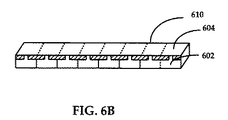
FIG. 6A is a plan view of one embodiment of a disclosed slider manufacturing method. The wafer 600 (AlTiC or silicon) is patterned with a series of deposited layers that form what will become sliders, and after processing is completed, each slider is placed above the embedded waveguide and the outer surface of the slider. A protrusion having an optical path changing element extending. Repeated patterning layers that later have projections, with embedded waveguides and optical path conversion elements (referred to here as projecting waveguide elements), deposit patterning layers after patterning techniques such as photolithography. Alternatively, it is formed on the
各々が突起導波路要素の1つのセットを有する突起部を含む複数のスライダ602は、図6Aに示されるように同時にパターン形成され得る。図6Aでは一連の7つのパターンがウェハ600にわたって図示されているが、典型的なウェハの両端にわたって多くのそれ以上のパターンが収められ得る。これらの一連のパターンは、ウェハから切削されてスライダバー610を形成し得る。一部の実施形態では、スライダバーは約60〜約70個のスライダを有し得、各スライダは、突起および突起導波路要素の1つのセットを含む。ウェハ600は、線620に沿ってスライスされて、ウェハから個々のスライダバー610を分離し得る。スライダバー610は、一端に突起を有する複数のスライダ602を有する。スライダバー610は、図6Bに示されるように複数のスライダ本体604を含む。
図6Cは、鉛直方位のスライダバー610を示す。スライダバー610は複数のスライダ本体604を含む。スライダ本体604の面上の領域615は、最終的に(さらなる処理後)、スライダの外面の上方に延びる突起となる領域を示す。斜線領域607は、スライダバー610から除去され、その後ダイシングされて、図6Dに図示するように個々のスライダ本体604を形成し得る。
FIG. 6C shows a
開示される装置を製造するための製造方法は、複数のスライダをウェハ上にパターン堆積するステップを含み、各スライダは、突起導波路要素を有する突起を含む。突起導波路要素は、たとえば、導波路および光路変換要素を含む。突起導波路要素は、突起内に一体的な部品として形成され得る。さらなる製造方法は、ウェハをスライスして、突起および突起導波路要素を有する複数のスライダ本体を含むスライダバーを製造するステップと、スライダ本体をパターンエッチングし、外面の上方に延びる突起を有するスライダを製造するステップと、突起および突起導波路要素を有する複数のスライダを含むスライダバーをダイシングし、個別のスライダ本体を製造するステップとを含む。 A manufacturing method for manufacturing the disclosed apparatus includes pattern depositing a plurality of sliders on a wafer, each slider including a protrusion having a protruding waveguide element. The protruding waveguide element includes, for example, a waveguide and an optical path conversion element. The protruding waveguide element can be formed as an integral part within the protrusion. A further manufacturing method includes slicing a wafer to manufacture a slider bar that includes a plurality of slider bodies having protrusions and protrusion waveguide elements, and pattern-etching the slider bodies and including sliders having protrusions extending above the outer surface. Manufacturing steps and dicing a slider bar including a plurality of sliders having protrusions and protruding waveguide elements to manufacture individual slider bodies.
一部の実施形態では、パターン堆積は、周知のフォトリソグラフィマスキングと、その後のエッチングおよび/または堆積とを含み得る。堆積は、蒸着、スパッタリング、プラズマ堆積、化学気相蒸着、または、当該技術分野で周知である光学もしくは電子材料を堆積する方法を含み得る。パターン堆積は、三次元印刷などの材料がパターン形成された堆積物を作製する他の方法も含み得る。パターンエッチングは、フォトリソグラフィまたは上記の堆積方法のいずれかによるマスク材料の堆積を用いて基板の一部をマスキングすることを含む。パターン堆積は、埋込導波路および/または光路変換要素を形成するために用いられ得る導波路材料およびクラッド材料のフォトリソグラフィおよび堆積の複数のステップを含み得る。一部の実施形態では、スライダ本体は傾斜エッチングされて(slope etched)、光路変換要素を形成し得る。エッチングは、イオンエッチング、反応性イオンエッチング、または、集積光学部品および電子部品の技術分野で周知の材料を除去する他の方法を用いて行なわれ得る。さらに、エッチングは、ラスターイオンビーム(rastered ion beam)を用いて達成されることもできる。 In some embodiments, pattern deposition can include well-known photolithography masking followed by etching and / or deposition. Deposition can include vapor deposition, sputtering, plasma deposition, chemical vapor deposition, or methods of depositing optical or electronic materials that are well known in the art. Pattern deposition can also include other methods of creating a patterned deposit of material, such as three-dimensional printing. Pattern etching involves masking a portion of the substrate using photolithography or deposition of mask material by any of the deposition methods described above. Pattern deposition can include multiple steps of photolithography and deposition of waveguide and cladding materials that can be used to form buried waveguides and / or optical path conversion elements. In some embodiments, the slider body can be slope etched to form an optical path conversion element. Etching can be performed using ion etching, reactive ion etching, or other methods that remove materials well known in the art of integrated optical and electronic components. In addition, etching can be accomplished using a rastered ion beam.
図7Aおよび図7Bは、開示されるスライダの減法的(subtractive)および加法的(additive)製造方法を図示する。図7Aは、突起707を含むスライダ本体704を図示する。突起707は、突起707内に埋込まれた導波路710を含む。突起707は光路変換要素705も含む。一部の実施形態では、光路変換要素705は、図7Aに示されるように、スライダ700の外面706上にあり得る。製造中、導波路710および光路変換要素705(本実施形態ではミラー)を含む突起707を形成する層は、矢印により示される方向に導波路材料を連続的にパターン形成および堆積することにより、スライダ本体704上に製造され得る。最終スライダ本体を作るために、パターン形成エッチングを用いて過剰な材料712をスライダ本体704から除去し、エッチング後にスライダ本体704の外面の上方に延びる突起707を製造することができる。
7A and 7B illustrate the disclosed subtractive and additive manufacturing methods of the slider. FIG. 7A illustrates a
図7Bは、加法的製造方法により開示されるスライダを作る方法を図示する。埋込導波路706は、上記と同様に、水平方向の矢印により示される方向に光学層を連続的にパターン形成および堆積することにより製造される。埋込導波路706は、スライダ704のエッジ709、たとえばトレーリングエッジと同一平面上にある。次に、光路変換要素705を含む突起708は、突起708が図示されるようにスライダ外面702の上方に延びるように、図7B中の鉛直方向矢印により示される方向の一連のパターン形成堆積物により形成される。突起708は、表面702と実質的に同一平面上である導波路部706aを含む。
FIG. 7B illustrates a method of making the slider disclosed by the additive manufacturing method. The embedded
開示される装置は、スライダの外面に対して実質的に平行に整列させられた光共振器を含む光源を含む。光源がレーザダイオードであるとき、この方位は、他の方位と比べて比較的長い光共振器、ひいてはより大きな出力を可能にする。一部の実施形態では、突起は、レーザダイオードの水平方向の位置合わせの止め部として作用し得る。開示される装置は、スライダの上面上に配置された複数のはんだバンプも含む。はんだバンプは、スライダの外面上に配置された光源からの光を電気的に、機械的に、および/または熱的に連結するように構成される。スライダの上面上に配置された少なくとも2つのはんだバンプは、少なくとも2つのはんだバンプのリフローに応じて、光源の出力光と導波路の入力部との間の位置合わせを容易にする。はんだバンプは、たとえば鉛直方向に、光源と導波路の入力部とのセルフアライメントを可能にする。はんだバンプは、水平方向の位置合わせにも役立ち得る。 The disclosed apparatus includes a light source that includes an optical resonator aligned substantially parallel to the outer surface of the slider. When the light source is a laser diode, this orientation allows a relatively long optical resonator and thus a larger output compared to other orientations. In some embodiments, the protrusion can act as a stop for horizontal alignment of the laser diode. The disclosed apparatus also includes a plurality of solder bumps disposed on the top surface of the slider. The solder bump is configured to electrically, mechanically and / or thermally couple light from a light source disposed on the outer surface of the slider. At least two solder bumps disposed on the top surface of the slider facilitate alignment between the output light of the light source and the input of the waveguide in response to reflow of the at least two solder bumps. The solder bumps enable self alignment of the light source and the input portion of the waveguide, for example, in the vertical direction. Solder bumps can also help in horizontal alignment.
本明細書中に引用されたすべての引用文献および公報は、それらが本開示と直接矛盾しない限り、その全体が引用により明確に本開示中に援用される。特定の実施形態を本明細書中に例示し、記載したが、本開示の範囲を逸脱することなく、さまざまな代替的なおよび/または同等の実施例が、図示および説明された特定の実施形態の代わりに行なわれ得ることが当業者であれば認識されるであろう。本出願は、ここに記載した特定の実施形態の如何なる適応またはバリエーションも包含することを意図する。したがって、本開示は、請求項およびその同等物によってのみ限定されることを意図する。本明細書中で引用されたすべての引用文献は、引用によりその全体がここに援用される。 All references and publications cited in this specification are expressly incorporated by reference into the present disclosure in their entirety, unless they are in direct conflict with the present disclosure. While specific embodiments have been illustrated and described herein, various alternative and / or equivalent examples may be illustrated and described without departing from the scope of the present disclosure. Those skilled in the art will recognize that this can be done instead. This application is intended to cover any adaptations or variations of the specific embodiments described herein. Accordingly, the present disclosure is intended to be limited only by the claims and equivalents thereof. All references cited herein are hereby incorporated by reference in their entirety.
200 HAMR装置、202 レーザダイオード、203 スライダ、205 外面、207 突起、209 光路変換要素、210 導波路、222 入力導波路、223A 全反射ミラ−、223B 部分反射ミラー、224 光共振器、230 リフローはんだバンプ 200 HAMR device, 202 laser diode, 203 slider, 205 outer surface, 207 protrusion, 209 optical path conversion element, 210 waveguide, 222 input waveguide, 223A total reflection mirror, 223B partial reflection mirror, 224 optical resonator, 230 reflow soldering bump
Claims (19)
スライダと、
前記スライダの外面上に配置された光源とを備え、前記光源は、前記スライダの前記外面に対して実質的に平行に整列された光共振器を含み、前記装置はさらに、
前記スライダの前記外面の上方に延びる突起を備え、前記突起は、前記光源に光結合された光路変換要素を含む、装置。 An apparatus, the apparatus comprising:
A slider,
A light source disposed on an outer surface of the slider, the light source including an optical resonator aligned substantially parallel to the outer surface of the slider, the apparatus further comprising:
An apparatus comprising a protrusion extending above the outer surface of the slider, the protrusion including an optical path conversion element optically coupled to the light source.
前記光共振器は、前記上面に実質的に平行に整列される、請求項1に記載の装置。 The outer surface of the slider includes a top surface, a bottom surface, a leading surface, a trailing surface, and two opposing side surfaces,
The apparatus of claim 1, wherein the optical resonator is aligned substantially parallel to the top surface.
前記光路変換要素は、前記スライダの外面と接するように構成される、請求項1に記載の装置。 The light source includes an optical resonator aligned substantially parallel to an upper surface of the slider;
The apparatus of claim 1, wherein the optical path changing element is configured to contact an outer surface of the slider.
前記突起は、前記光源と前記導波路との位置合わせ用の止め部として機能するように構成される、請求項1に記載の装置。 The slider includes a waveguide;
The apparatus of claim 1, wherein the protrusion is configured to function as a stop for alignment of the light source and the waveguide.
前記スライダの前記上面に配置された少なくとも2つのはんだバンプは、前記少なくとも2つのはんだバンプのリフローに応じて、前記光源の出力光と前記導波路の入力部との間の位置合わせを容易にする、請求項12に記載の装置。 The protrusion includes a waveguide;
At least two solder bumps disposed on the top surface of the slider facilitate alignment between the output light of the light source and the input portion of the waveguide in response to reflow of the at least two solder bumps. The apparatus according to claim 12.
導波路要素の複数のセットをウェハ上にパターン堆積するステップを備え、前記導波路要素の各セットは、その突起部中に光路変換要素を含み、前記方法はさらに、
前記ウェハをスライスして、前記導波路要素の前記複数のセットの一部を含むスライダバーを製造するステップと、
前記スライダバーをパターンエッチングして、スライダを製造するステップとを含み、各スライダは外面の上方に延びる突起を有し、前記突起は前記導波路要素の1つのセットを備え、前記方法はさらに、
前記スライダバーをダイシングして、スライダ本体を製造するステップを備える、方法。 A method, the method comprising:
Pattern-depositing a plurality of sets of waveguide elements on a wafer, each set of waveguide elements including an optical path converting element in its protrusion, the method further comprising:
Slicing the wafer to produce a slider bar including a portion of the plurality of sets of the waveguide elements;
Patterning the slider bar to produce sliders, each slider having a protrusion extending above an outer surface, the protrusion comprising a set of waveguide elements, the method further comprising:
Dicing the slider bar to produce a slider body.
スライダを提供するステップを備え、前記スライダは、外面およびトレーリングエッジと、前記スライダの前記トレーリングエッジに沿って配置された光導波路とを有し、前記方法はさらに、
前記トレーリングエッジに実質的に垂直な方向に、前記スライダの前記外面の上方に突起をパターン堆積するステップを備え、前記突起は、前記光導波路に光結合された光路変換要素を含む、方法。 A method, the method comprising:
Providing a slider, the slider having an outer surface and a trailing edge, and an optical waveguide disposed along the trailing edge of the slider, the method further comprising:
Patterning a protrusion over the outer surface of the slider in a direction substantially perpendicular to the trailing edge, the protrusion including an optical path changing element optically coupled to the optical waveguide.
Applications Claiming Priority (2)
| Application Number | Priority Date | Filing Date | Title |
|---|---|---|---|
| US13/967,824 US9202501B2 (en) | 2013-08-15 | 2013-08-15 | Slider for magnetic recording apparatus with projection comprising optical turning element and methods of fabrication thereof |
| US13/967,824 | 2013-08-15 |
Publications (2)
| Publication Number | Publication Date |
|---|---|
| JP2015038798A true JP2015038798A (en) | 2015-02-26 |
| JP2015038798A5 JP2015038798A5 (en) | 2017-09-28 |
Family
ID=52466753
Family Applications (1)
| Application Number | Title | Priority Date | Filing Date |
|---|---|---|---|
| JP2014165195A Pending JP2015038798A (en) | 2013-08-15 | 2014-08-14 | Magnetic recording apparatus and method of manufacturing the same |
Country Status (4)
| Country | Link |
|---|---|
| US (2) | US9202501B2 (en) |
| JP (1) | JP2015038798A (en) |
| KR (1) | KR101595723B1 (en) |
| CN (1) | CN104376852B (en) |
Families Citing this family (5)
| Publication number | Priority date | Publication date | Assignee | Title |
|---|---|---|---|---|
| US9202501B2 (en) | 2013-08-15 | 2015-12-01 | Seagate Technology Llc | Slider for magnetic recording apparatus with projection comprising optical turning element and methods of fabrication thereof |
| US9659589B2 (en) * | 2015-09-29 | 2017-05-23 | Western Digital (Fremont), Llc | Free-standing reflector usable in heat assisted magnetic recording technology |
| US10058890B1 (en) | 2015-11-20 | 2018-08-28 | Seagate Technology Llc | Methods of forming an air bearing surface on a slider and related sliders |
| US9830937B1 (en) | 2016-01-22 | 2017-11-28 | Seagate Technology Llc | Horizontal cavity surface emitting laser assembly features for heat assisted magnetic recording |
| US10943613B1 (en) * | 2020-03-13 | 2021-03-09 | Sae Magnetics (H.K.) Ltd. | Thermally assisted magnetic head, head gimbal assembly, hard disk drive and method of manufacturing the thermally assisted magnetic head |
Citations (5)
| Publication number | Priority date | Publication date | Assignee | Title |
|---|---|---|---|---|
| JP2008010093A (en) * | 2006-06-30 | 2008-01-17 | Tdk Corp | Thin film heat assisted magnetic recording head |
| JP2012234615A (en) * | 2011-04-29 | 2012-11-29 | Seagate Technology Llc | Method and apparatus for aligning laser diode on slider |
| WO2012176498A1 (en) * | 2011-06-22 | 2012-12-27 | コニカミノルタアドバンストレイヤー株式会社 | Method for adjusting position of optical element |
| JP2013077369A (en) * | 2011-09-29 | 2013-04-25 | Seagate Technology Llc | Waveguide, head and disk drive |
| JP2013140671A (en) * | 2013-04-24 | 2013-07-18 | Hitachi Ltd | Head for thermally-assisted recording, and thermal assisted recording device |
Family Cites Families (34)
| Publication number | Priority date | Publication date | Assignee | Title |
|---|---|---|---|---|
| JP2000173035A (en) | 1998-12-02 | 2000-06-23 | Toshiba Corp | Head ginbal assembly and magnetic disc drive |
| US6404706B1 (en) | 1999-02-12 | 2002-06-11 | Read-Rite Corporation | Laser mounting for a thermally assisted GMR head |
| US6873576B1 (en) * | 2000-05-24 | 2005-03-29 | Koninklijke Philips Electronics N.V. | Method of thermally-assisted data recording and a recording apparatus |
| JP4325172B2 (en) * | 2002-11-01 | 2009-09-02 | 株式会社日立製作所 | Near-field light generating probe and near-field light generating apparatus |
| US7310206B2 (en) * | 2004-12-28 | 2007-12-18 | Sae Magnetics (H.K.) Ltd. | Magnetic thin film head with heat-assisted write section and hard disk drive incorporating same |
| US8339905B2 (en) | 2005-04-13 | 2012-12-25 | Seagate Technology Llc | Alignment features for heat assisted magnetic recording transducers |
| JP4129031B2 (en) * | 2006-06-12 | 2008-07-30 | 株式会社日立製作所 | Near-field light generator and recording / reproducing apparatus |
| JP2008059645A (en) | 2006-08-30 | 2008-03-13 | Hitachi Ltd | Recording head |
| KR100831051B1 (en) | 2007-01-10 | 2008-05-21 | 삼성전자주식회사 | Waveguide structure and method of fabrication thereof, and heat assisted magnetic recording head using thereof |
| JP5085988B2 (en) * | 2007-06-21 | 2012-11-28 | 株式会社日立製作所 | Manufacturing method of optical element integrated head |
| US7949218B2 (en) * | 2008-02-14 | 2011-05-24 | Seagate Technology Llc | Waveguide for heat assisted magnetic recording |
| JP2010146655A (en) | 2008-12-19 | 2010-07-01 | Hitachi Global Storage Technologies Netherlands Bv | Optical assist magnetic recording head and manufacturing method thereof |
| US8254212B2 (en) | 2009-06-25 | 2012-08-28 | Seagate Technology Llc | Integrated heat assisted magnetic recording device |
| US8395971B2 (en) | 2009-07-15 | 2013-03-12 | Headway Technologies, Inc. | Heat-assisted magnetic recording head with laser diode fixed to slider |
| US8406089B2 (en) | 2009-09-04 | 2013-03-26 | Headway Technologies, Inc. | Heat-assisted magnetic recording head with laser diode fixed to slider |
| KR20110027414A (en) | 2009-09-10 | 2011-03-16 | 엘지전자 주식회사 | Air conditioner |
| US8107192B2 (en) | 2009-10-23 | 2012-01-31 | Headway Technologies, Inc. | Heat-assisted magnetic recording head with laser diode fixed to slider |
| US8385183B2 (en) * | 2009-11-05 | 2013-02-26 | Seagate Technology, Llc | Light delivery waveguide |
| JP5322898B2 (en) * | 2009-11-25 | 2013-10-23 | 株式会社日立製作所 | Thermally assisted magnetic head slider and head gimbal assembly |
| JP2011187111A (en) | 2010-03-05 | 2011-09-22 | Hitachi Ltd | Head for thermally-assisted magnetic recording, and thermal assisted magnetic recording device |
| US9065236B2 (en) | 2010-04-30 | 2015-06-23 | Seagate Technology | Method and apparatus for aligning a laser diode on a slider |
| US8345517B2 (en) | 2010-04-30 | 2013-01-01 | Seagate Technology Llc | Method and apparatus for aligning a laser diode on a slider |
| WO2012014594A1 (en) * | 2010-07-30 | 2012-02-02 | コニカミノルタオプト株式会社 | Optical element, production method, light-assisted magnetic recording head, and magnetic recording device |
| JP5520736B2 (en) * | 2010-07-30 | 2014-06-11 | 株式会社日立ハイテクノロジーズ | Defect inspection method and defect inspection apparatus |
| JP5439316B2 (en) * | 2010-08-30 | 2014-03-12 | 株式会社日立製作所 | Thermally assisted recording head and magnetic recording apparatus |
| US8611193B2 (en) * | 2010-10-20 | 2013-12-17 | Seagate Technology Llc | Method and apparatus for coupling a laser diode to a magnetic writer |
| US8194512B2 (en) * | 2010-11-08 | 2012-06-05 | Hitachi Global Storage Technologies Netherlands B.V. | Head structure for thermally-assisted recording (TAR) disk drive |
| US8107326B1 (en) | 2010-11-15 | 2012-01-31 | Hitachi Global Storage Technologies Netherlands B.V. | Slider with integrated thermally-assisted recording (TAR) head and integrated long laser diode |
| US8379494B2 (en) | 2011-02-03 | 2013-02-19 | Seagate Technology Llc | Laser-in slider light delivery for heat assisted magnetic recording |
| US8270256B1 (en) * | 2011-05-06 | 2012-09-18 | Hitachi Global Storage Technologies Netherland B.V. | Magnetic recording disk drive with shingled writing and wide-area thermal assistance |
| US20130142478A1 (en) * | 2011-12-02 | 2013-06-06 | Seagate Technology Llc | Method and apparatus for aligning a laser diode on a slider structure |
| US8456969B1 (en) | 2012-03-27 | 2013-06-04 | Seagate Technology Llc | Laser integrated recording head for heat assisted magnetic recording |
| US20130279310A1 (en) * | 2012-04-24 | 2013-10-24 | Seagate Technology Llc | Antireflection coating for slider |
| US9202501B2 (en) | 2013-08-15 | 2015-12-01 | Seagate Technology Llc | Slider for magnetic recording apparatus with projection comprising optical turning element and methods of fabrication thereof |
-
2013
- 2013-08-15 US US13/967,824 patent/US9202501B2/en not_active Expired - Fee Related
-
2014
- 2014-08-13 KR KR1020140105104A patent/KR101595723B1/en active IP Right Grant
- 2014-08-14 CN CN201410399939.XA patent/CN104376852B/en active Active
- 2014-08-14 JP JP2014165195A patent/JP2015038798A/en active Pending
-
2015
- 2015-11-12 US US14/939,004 patent/US9336801B2/en active Active
Patent Citations (5)
| Publication number | Priority date | Publication date | Assignee | Title |
|---|---|---|---|---|
| JP2008010093A (en) * | 2006-06-30 | 2008-01-17 | Tdk Corp | Thin film heat assisted magnetic recording head |
| JP2012234615A (en) * | 2011-04-29 | 2012-11-29 | Seagate Technology Llc | Method and apparatus for aligning laser diode on slider |
| WO2012176498A1 (en) * | 2011-06-22 | 2012-12-27 | コニカミノルタアドバンストレイヤー株式会社 | Method for adjusting position of optical element |
| JP2013077369A (en) * | 2011-09-29 | 2013-04-25 | Seagate Technology Llc | Waveguide, head and disk drive |
| JP2013140671A (en) * | 2013-04-24 | 2013-07-18 | Hitachi Ltd | Head for thermally-assisted recording, and thermal assisted recording device |
Also Published As
| Publication number | Publication date |
|---|---|
| US9202501B2 (en) | 2015-12-01 |
| CN104376852B (en) | 2018-06-05 |
| US20150049595A1 (en) | 2015-02-19 |
| KR20150020122A (en) | 2015-02-25 |
| US20160064019A1 (en) | 2016-03-03 |
| KR101595723B1 (en) | 2016-02-19 |
| CN104376852A (en) | 2015-02-25 |
| US9336801B2 (en) | 2016-05-10 |
Similar Documents
| Publication | Publication Date | Title |
|---|---|---|
| US9626991B2 (en) | Near-field transducer with enlarged region, peg region, and heat sink region | |
| US8649245B2 (en) | Direct waveguide light delivery to NFT for heat assisted magnetic recording | |
| US9502069B2 (en) | Plasmonic transducer having two metal elements with a gap disposed therebetween | |
| JP5777585B2 (en) | Apparatus, method, and system with waveguide | |
| US9378757B2 (en) | Methods of making a near field transducer with a flare peg | |
| US8451705B2 (en) | Plasmonic transducer having two metal elements with a gap disposed therebetween | |
| US8730780B2 (en) | Light delivery waveguide | |
| US9632242B2 (en) | Light delivery guide | |
| US8929698B2 (en) | Plasmonic transducer with reduced cross section at media-reading surface | |
| US8395972B2 (en) | Thermally assisted magnetic head, head gimbal assembly, and hard disk drive | |
| US20140376345A1 (en) | Near field transducer with isolated peg | |
| US8699307B2 (en) | Near-field transducer | |
| JP2011008908A (en) | Heat-assisted magnetic recording device, and method for fabricating integrated heat-assisted magnetic recording device | |
| US9336801B2 (en) | Slider for magnetic recording apparatus with projection comprising optical turning element and methods of fabrication thereof | |
| JP2011159374A (en) | Heat-assisted magnetic recording head with convergent lens | |
| JP5689009B2 (en) | Method for manufacturing plasmon conversion element |
Legal Events
| Date | Code | Title | Description |
|---|---|---|---|
| A521 | Request for written amendment filed |
Free format text: JAPANESE INTERMEDIATE CODE: A523 Effective date: 20170814 |
|
| A621 | Written request for application examination |
Free format text: JAPANESE INTERMEDIATE CODE: A621 Effective date: 20170814 |
|
| A977 | Report on retrieval |
Free format text: JAPANESE INTERMEDIATE CODE: A971007 Effective date: 20180614 |
|
| A131 | Notification of reasons for refusal |
Free format text: JAPANESE INTERMEDIATE CODE: A131 Effective date: 20180717 |
|
| A02 | Decision of refusal |
Free format text: JAPANESE INTERMEDIATE CODE: A02 Effective date: 20190409 |