JP2015018596A - Phase change memory materials - Google Patents
Phase change memory materials Download PDFInfo
- Publication number
- JP2015018596A JP2015018596A JP2014146705A JP2014146705A JP2015018596A JP 2015018596 A JP2015018596 A JP 2015018596A JP 2014146705 A JP2014146705 A JP 2014146705A JP 2014146705 A JP2014146705 A JP 2014146705A JP 2015018596 A JP2015018596 A JP 2015018596A
- Authority
- JP
- Japan
- Prior art keywords
- phase change
- change memory
- phase
- atomic percent
- thin film
- Prior art date
- Legal status (The legal status is an assumption and is not a legal conclusion. Google has not performed a legal analysis and makes no representation as to the accuracy of the status listed.)
- Granted
Links
- 239000000463 material Substances 0.000 title claims abstract description 53
- 239000010409 thin film Substances 0.000 claims abstract description 24
- 229910052738 indium Inorganic materials 0.000 claims abstract description 17
- 229910052782 aluminium Inorganic materials 0.000 claims abstract description 16
- 229910052733 gallium Inorganic materials 0.000 claims abstract description 16
- 229910052745 lead Inorganic materials 0.000 claims abstract description 16
- 229910052711 selenium Inorganic materials 0.000 claims abstract description 16
- 229910052710 silicon Inorganic materials 0.000 claims abstract description 16
- 229910052717 sulfur Inorganic materials 0.000 claims abstract description 16
- 229910052716 thallium Inorganic materials 0.000 claims abstract description 16
- 229910052718 tin Inorganic materials 0.000 claims abstract description 16
- 229910052785 arsenic Inorganic materials 0.000 claims abstract description 15
- 229910052787 antimony Inorganic materials 0.000 claims abstract description 14
- 238000000034 method Methods 0.000 claims abstract description 12
- 239000000758 substrate Substances 0.000 claims abstract description 9
- 229910052714 tellurium Inorganic materials 0.000 claims abstract description 6
- 238000004549 pulsed laser deposition Methods 0.000 claims abstract description 5
- 239000013078 crystal Substances 0.000 claims description 15
- XSOKHXFFCGXDJZ-UHFFFAOYSA-N telluride(2-) Chemical compound [Te-2] XSOKHXFFCGXDJZ-UHFFFAOYSA-N 0.000 abstract description 2
- 239000000203 mixture Substances 0.000 description 22
- 238000010438 heat treatment Methods 0.000 description 18
- 239000011521 glass Substances 0.000 description 13
- 238000002441 X-ray diffraction Methods 0.000 description 7
- 238000002310 reflectometry Methods 0.000 description 7
- 229910005900 GeTe Inorganic materials 0.000 description 4
- 238000002425 crystallisation Methods 0.000 description 4
- 230000008025 crystallization Effects 0.000 description 4
- 230000015572 biosynthetic process Effects 0.000 description 3
- 239000002419 bulk glass Substances 0.000 description 3
- 238000004093 laser heating Methods 0.000 description 3
- 230000008018 melting Effects 0.000 description 3
- 238000002844 melting Methods 0.000 description 3
- 229910000618 GeSbTe Inorganic materials 0.000 description 2
- FAPWRFPIFSIZLT-UHFFFAOYSA-M Sodium chloride Chemical compound [Na+].[Cl-] FAPWRFPIFSIZLT-UHFFFAOYSA-M 0.000 description 2
- 238000006243 chemical reaction Methods 0.000 description 2
- 239000010408 film Substances 0.000 description 2
- 230000006698 induction Effects 0.000 description 2
- 238000012986 modification Methods 0.000 description 2
- 230000004048 modification Effects 0.000 description 2
- 230000006911 nucleation Effects 0.000 description 2
- 238000010899 nucleation Methods 0.000 description 2
- 239000012782 phase change material Substances 0.000 description 2
- 229910000927 Ge alloy Inorganic materials 0.000 description 1
- 229910005872 GeSb Inorganic materials 0.000 description 1
- 229910001245 Sb alloy Inorganic materials 0.000 description 1
- 229910001215 Te alloy Inorganic materials 0.000 description 1
- 238000002679 ablation Methods 0.000 description 1
- 239000003708 ampul Substances 0.000 description 1
- 239000000919 ceramic Substances 0.000 description 1
- 239000005387 chalcogenide glass Substances 0.000 description 1
- 150000004770 chalcogenides Chemical class 0.000 description 1
- 150000001875 compounds Chemical class 0.000 description 1
- 238000013500 data storage Methods 0.000 description 1
- 238000000151 deposition Methods 0.000 description 1
- 230000008021 deposition Effects 0.000 description 1
- 238000010586 diagram Methods 0.000 description 1
- 238000000113 differential scanning calorimetry Methods 0.000 description 1
- 229910052732 germanium Inorganic materials 0.000 description 1
- 239000002241 glass-ceramic Substances 0.000 description 1
- 229910052737 gold Inorganic materials 0.000 description 1
- 238000001341 grazing-angle X-ray diffraction Methods 0.000 description 1
- 238000001755 magnetron sputter deposition Methods 0.000 description 1
- 230000014759 maintenance of location Effects 0.000 description 1
- 239000002184 metal Substances 0.000 description 1
- 229910052751 metal Inorganic materials 0.000 description 1
- 230000003287 optical effect Effects 0.000 description 1
- 229920000642 polymer Polymers 0.000 description 1
- 235000002639 sodium chloride Nutrition 0.000 description 1
- 239000011780 sodium chloride Substances 0.000 description 1
- 239000007787 solid Substances 0.000 description 1
- PORWMNRCUJJQNO-UHFFFAOYSA-N tellurium atom Chemical compound [Te] PORWMNRCUJJQNO-UHFFFAOYSA-N 0.000 description 1
- 238000002207 thermal evaporation Methods 0.000 description 1
- 230000007704 transition Effects 0.000 description 1
- 238000011179 visual inspection Methods 0.000 description 1
Images


Classifications
-
- G—PHYSICS
- G11—INFORMATION STORAGE
- G11B—INFORMATION STORAGE BASED ON RELATIVE MOVEMENT BETWEEN RECORD CARRIER AND TRANSDUCER
- G11B7/00—Recording or reproducing by optical means, e.g. recording using a thermal beam of optical radiation by modifying optical properties or the physical structure, reproducing using an optical beam at lower power by sensing optical properties; Record carriers therefor
- G11B7/24—Record carriers characterised by shape, structure or physical properties, or by the selection of the material
- G11B7/241—Record carriers characterised by shape, structure or physical properties, or by the selection of the material characterised by the selection of the material
- G11B7/242—Record carriers characterised by shape, structure or physical properties, or by the selection of the material characterised by the selection of the material of recording layers
- G11B7/243—Record carriers characterised by shape, structure or physical properties, or by the selection of the material characterised by the selection of the material of recording layers comprising inorganic materials only, e.g. ablative layers
- G11B7/2433—Metals or elements of Groups 13, 14, 15 or 16 of the Periodic Table, e.g. B, Si, Ge, As, Sb, Bi, Se or Te
-
- H—ELECTRICITY
- H10—SEMICONDUCTOR DEVICES; ELECTRIC SOLID-STATE DEVICES NOT OTHERWISE PROVIDED FOR
- H10N—ELECTRIC SOLID-STATE DEVICES NOT OTHERWISE PROVIDED FOR
- H10N70/00—Solid-state devices having no potential barriers, and specially adapted for rectifying, amplifying, oscillating or switching
- H10N70/011—Manufacture or treatment of multistable switching devices
- H10N70/021—Formation of switching materials, e.g. deposition of layers
- H10N70/026—Formation of switching materials, e.g. deposition of layers by physical vapor deposition, e.g. sputtering
-
- H—ELECTRICITY
- H10—SEMICONDUCTOR DEVICES; ELECTRIC SOLID-STATE DEVICES NOT OTHERWISE PROVIDED FOR
- H10N—ELECTRIC SOLID-STATE DEVICES NOT OTHERWISE PROVIDED FOR
- H10N70/00—Solid-state devices having no potential barriers, and specially adapted for rectifying, amplifying, oscillating or switching
- H10N70/20—Multistable switching devices, e.g. memristors
- H10N70/231—Multistable switching devices, e.g. memristors based on solid-state phase change, e.g. between amorphous and crystalline phases, Ovshinsky effect
-
- H—ELECTRICITY
- H10—SEMICONDUCTOR DEVICES; ELECTRIC SOLID-STATE DEVICES NOT OTHERWISE PROVIDED FOR
- H10N—ELECTRIC SOLID-STATE DEVICES NOT OTHERWISE PROVIDED FOR
- H10N70/00—Solid-state devices having no potential barriers, and specially adapted for rectifying, amplifying, oscillating or switching
- H10N70/801—Constructional details of multistable switching devices
- H10N70/881—Switching materials
- H10N70/882—Compounds of sulfur, selenium or tellurium, e.g. chalcogenides
- H10N70/8828—Tellurides, e.g. GeSbTe
-
- G—PHYSICS
- G11—INFORMATION STORAGE
- G11B—INFORMATION STORAGE BASED ON RELATIVE MOVEMENT BETWEEN RECORD CARRIER AND TRANSDUCER
- G11B7/00—Recording or reproducing by optical means, e.g. recording using a thermal beam of optical radiation by modifying optical properties or the physical structure, reproducing using an optical beam at lower power by sensing optical properties; Record carriers therefor
- G11B7/24—Record carriers characterised by shape, structure or physical properties, or by the selection of the material
- G11B7/241—Record carriers characterised by shape, structure or physical properties, or by the selection of the material characterised by the selection of the material
- G11B7/242—Record carriers characterised by shape, structure or physical properties, or by the selection of the material characterised by the selection of the material of recording layers
- G11B7/243—Record carriers characterised by shape, structure or physical properties, or by the selection of the material characterised by the selection of the material of recording layers comprising inorganic materials only, e.g. ablative layers
- G11B2007/24302—Metals or metalloids
- G11B2007/24312—Metals or metalloids group 14 elements (e.g. Si, Ge, Sn)
-
- G—PHYSICS
- G11—INFORMATION STORAGE
- G11B—INFORMATION STORAGE BASED ON RELATIVE MOVEMENT BETWEEN RECORD CARRIER AND TRANSDUCER
- G11B7/00—Recording or reproducing by optical means, e.g. recording using a thermal beam of optical radiation by modifying optical properties or the physical structure, reproducing using an optical beam at lower power by sensing optical properties; Record carriers therefor
- G11B7/24—Record carriers characterised by shape, structure or physical properties, or by the selection of the material
- G11B7/241—Record carriers characterised by shape, structure or physical properties, or by the selection of the material characterised by the selection of the material
- G11B7/242—Record carriers characterised by shape, structure or physical properties, or by the selection of the material characterised by the selection of the material of recording layers
- G11B7/243—Record carriers characterised by shape, structure or physical properties, or by the selection of the material characterised by the selection of the material of recording layers comprising inorganic materials only, e.g. ablative layers
- G11B2007/24302—Metals or metalloids
- G11B2007/24314—Metals or metalloids group 15 elements (e.g. Sb, Bi)
-
- G—PHYSICS
- G11—INFORMATION STORAGE
- G11B—INFORMATION STORAGE BASED ON RELATIVE MOVEMENT BETWEEN RECORD CARRIER AND TRANSDUCER
- G11B7/00—Recording or reproducing by optical means, e.g. recording using a thermal beam of optical radiation by modifying optical properties or the physical structure, reproducing using an optical beam at lower power by sensing optical properties; Record carriers therefor
- G11B7/24—Record carriers characterised by shape, structure or physical properties, or by the selection of the material
- G11B7/241—Record carriers characterised by shape, structure or physical properties, or by the selection of the material characterised by the selection of the material
- G11B7/242—Record carriers characterised by shape, structure or physical properties, or by the selection of the material characterised by the selection of the material of recording layers
- G11B7/243—Record carriers characterised by shape, structure or physical properties, or by the selection of the material characterised by the selection of the material of recording layers comprising inorganic materials only, e.g. ablative layers
- G11B2007/24302—Metals or metalloids
- G11B2007/24316—Metals or metalloids group 16 elements (i.e. chalcogenides, Se, Te)
-
- G—PHYSICS
- G11—INFORMATION STORAGE
- G11B—INFORMATION STORAGE BASED ON RELATIVE MOVEMENT BETWEEN RECORD CARRIER AND TRANSDUCER
- G11B7/00—Recording or reproducing by optical means, e.g. recording using a thermal beam of optical radiation by modifying optical properties or the physical structure, reproducing using an optical beam at lower power by sensing optical properties; Record carriers therefor
- G11B7/24—Record carriers characterised by shape, structure or physical properties, or by the selection of the material
- G11B7/241—Record carriers characterised by shape, structure or physical properties, or by the selection of the material characterised by the selection of the material
- G11B7/252—Record carriers characterised by shape, structure or physical properties, or by the selection of the material characterised by the selection of the material of layers other than recording layers
- G11B7/253—Record carriers characterised by shape, structure or physical properties, or by the selection of the material characterised by the selection of the material of layers other than recording layers of substrates
-
- Y—GENERAL TAGGING OF NEW TECHNOLOGICAL DEVELOPMENTS; GENERAL TAGGING OF CROSS-SECTIONAL TECHNOLOGIES SPANNING OVER SEVERAL SECTIONS OF THE IPC; TECHNICAL SUBJECTS COVERED BY FORMER USPC CROSS-REFERENCE ART COLLECTIONS [XRACs] AND DIGESTS
- Y10—TECHNICAL SUBJECTS COVERED BY FORMER USPC
- Y10T—TECHNICAL SUBJECTS COVERED BY FORMER US CLASSIFICATION
- Y10T428/00—Stock material or miscellaneous articles
- Y10T428/12—All metal or with adjacent metals
- Y10T428/12493—Composite; i.e., plural, adjacent, spatially distinct metal components [e.g., layers, joint, etc.]
- Y10T428/12674—Ge- or Si-base component
-
- Y—GENERAL TAGGING OF NEW TECHNOLOGICAL DEVELOPMENTS; GENERAL TAGGING OF CROSS-SECTIONAL TECHNOLOGIES SPANNING OVER SEVERAL SECTIONS OF THE IPC; TECHNICAL SUBJECTS COVERED BY FORMER USPC CROSS-REFERENCE ART COLLECTIONS [XRACs] AND DIGESTS
- Y10—TECHNICAL SUBJECTS COVERED BY FORMER USPC
- Y10T—TECHNICAL SUBJECTS COVERED BY FORMER US CLASSIFICATION
- Y10T428/00—Stock material or miscellaneous articles
- Y10T428/12—All metal or with adjacent metals
- Y10T428/12493—Composite; i.e., plural, adjacent, spatially distinct metal components [e.g., layers, joint, etc.]
- Y10T428/12681—Ga-, In-, Tl- or Group VA metal-base component
-
- Y—GENERAL TAGGING OF NEW TECHNOLOGICAL DEVELOPMENTS; GENERAL TAGGING OF CROSS-SECTIONAL TECHNOLOGIES SPANNING OVER SEVERAL SECTIONS OF THE IPC; TECHNICAL SUBJECTS COVERED BY FORMER USPC CROSS-REFERENCE ART COLLECTIONS [XRACs] AND DIGESTS
- Y10—TECHNICAL SUBJECTS COVERED BY FORMER USPC
- Y10T—TECHNICAL SUBJECTS COVERED BY FORMER US CLASSIFICATION
- Y10T428/00—Stock material or miscellaneous articles
- Y10T428/21—Circular sheet or circular blank
-
- Y—GENERAL TAGGING OF NEW TECHNOLOGICAL DEVELOPMENTS; GENERAL TAGGING OF CROSS-SECTIONAL TECHNOLOGIES SPANNING OVER SEVERAL SECTIONS OF THE IPC; TECHNICAL SUBJECTS COVERED BY FORMER USPC CROSS-REFERENCE ART COLLECTIONS [XRACs] AND DIGESTS
- Y10—TECHNICAL SUBJECTS COVERED BY FORMER USPC
- Y10T—TECHNICAL SUBJECTS COVERED BY FORMER US CLASSIFICATION
- Y10T428/00—Stock material or miscellaneous articles
- Y10T428/31504—Composite [nonstructural laminate]
- Y10T428/31678—Of metal
Landscapes
- Chemical & Material Sciences (AREA)
- Inorganic Chemistry (AREA)
- Engineering & Computer Science (AREA)
- Manufacturing & Machinery (AREA)
- Optical Record Carriers And Manufacture Thereof (AREA)
- Thermal Transfer Or Thermal Recording In General (AREA)
- Semiconductor Memories (AREA)
- Physical Vapour Deposition (AREA)
- Manufacturing Optical Record Carriers (AREA)
- Glass Compositions (AREA)
Abstract
Description
本出願は、2008年8月29日に出願された米国仮特許出願第61/092868号および2009年7月15日に出願された米国特許出願12/503156号に基づく優先権を主張するものであり、特願2011−525009を原出願とする分割出願である。 This application claims priority based on US Provisional Patent Application No. 61/092868 filed on August 29, 2008 and US Patent Application No. 12/503156 filed on July 15, 2009. Yes, it is a divisional application whose original application is Japanese Patent Application No. 2011-525209.
本発明の実施の形態は、相変化記憶材料およびより詳しくは、相変化記憶用途、例えば、光学データおよび電子データの記憶のために有用なテルル化GeAs材料に関する。 Embodiments of the present invention relate to phase change memory materials and, more particularly, to tellurium GeAs materials useful for phase change memory applications such as optical and electronic data storage.
従来の相変化記憶装置では、別個の性質を有する二相の間で変化できる材料を利用している。それらの材料は典型的に非晶相から結晶相に変化でき、それらの相は、著しく異なる性質、例えば、異なる抵抗率、導電率および/または反射率を有し得る。 Conventional phase change memory devices utilize materials that can change between two phases having distinct properties. The materials can typically change from an amorphous phase to a crystalline phase, which can have significantly different properties, such as different resistivity, conductivity and / or reflectivity.
非晶相から結晶相への相変化は、非晶性材料を、核生成、結晶の形成、次いで、結晶化を促進する温度まで加熱することによって行うことができる。非晶性に戻る相変化は、結晶相を溶融温度より高い温度まで加熱することによって行うことができる。 The phase change from the amorphous phase to the crystalline phase can be performed by heating the amorphous material to a temperature that promotes nucleation, crystal formation, and then crystallization. The phase change back to amorphous can be performed by heating the crystalline phase to a temperature higher than the melting temperature.
カルコゲナイド材料、例えば、Ge,SbおよびTe合金が、書き込み可能ディスクに情報を記憶させるためなどの相変化記憶用途に現在使用されている。 Chalcogenide materials, such as Ge, Sb, and Te alloys, are currently used for phase change storage applications, such as for storing information on a writable disk.
これまで確認されているいくつかの相変化記憶材料が、松下/パナソニックおよびIBMの研究者によって開発されてきた。代表的な材料としては、GeTe−Sb2Te3接合(join)、特にGe2Sb2Te5(GST)、およびAu,In添加テルル化Sb(AIST)が挙げられる。これらの材料は、レーザ加熱または電流パルスの下で、高導電率、高反射率の結晶相と低導電率、低反射率の非晶相との間で約10nsの時間スケールで循環させることができる。 Several phase change memory materials that have been identified have been developed by Matsushita / Panasonic and IBM researchers. Typical materials include GeTe—Sb 2 Te 3 joins, especially Ge 2 Sb 2 Te 5 (GST), and Au, In doped telluride Sb (AIST). These materials can be circulated on a time scale of about 10 ns between a high conductivity, high reflectivity crystalline phase and a low conductivity, low reflectivity amorphous phase under laser heating or current pulses. it can.
GSTおよびAISTなどのいくつかの従来の材料は、不揮発性記憶用途にとって良好な性質を有するが、より速い相転移および/またはより長い書き込み/書き換え可能性を有する相変化記憶材料を有することが都合よいであろう。 Some conventional materials such as GST and AIST have good properties for non-volatile memory applications, but it is advantageous to have phase change memory materials with faster phase transitions and / or longer writability / rewritability. Would be good.
本発明の実施の形態は、標準的なGeSbTe系の範囲から外れた、相変化記憶用途のためのGeAsTe系組成物である。さらに、特定のGeAsTe組成物はバルクガラスに製造できるので、GeAsTe非晶相の安定性は、バルクガラスの形成が可能ではないGeSbTe類似物のものよりも大きい傾向にある。この特徴により、導電率/反射率の対比の劣化がなく、書き込み/書き換え周期が増加し、データ保持がより長くなるであろう。 Embodiments of the present invention are GeAsTe-based compositions for phase change memory applications that deviate from the standard GeSbTe-based range. Furthermore, because certain GeAsTe compositions can be made into bulk glass, the stability of the GeAsTe amorphous phase tends to be greater than that of GeSbTe analogs where bulk glass formation is not possible. This feature will not degrade the conductivity / reflectance contrast, increase the write / rewrite cycle, and make data retention longer.
本発明の1つの実施の形態は、少なくとも1つの六方晶相を有する組成物からなる結晶化薄膜、または結晶化形態で少なくとも1つの六方晶相を有することのできる結晶化可能な組成物を備えた物品である。 One embodiment of the present invention comprises a crystallized thin film comprising a composition having at least one hexagonal phase, or a crystallizable composition capable of having at least one hexagonal phase in crystallized form. Goods.
本発明の別の実施の形態は、相変化記憶非晶性材料からなる薄膜を提供し、この相変化記憶非晶性材料を六方晶結晶相に転化させる各工程を有してなる方法である。 Another embodiment of the present invention is a method comprising the steps of providing a thin film comprising a phase change memory amorphous material and converting the phase change memory amorphous material to a hexagonal crystal phase. .
本発明のさらに別の実施の形態は、六方晶結晶相を有する相変化記憶材料からなる薄膜を提供し、この六方晶結晶相を非晶相に転化させる各工程を有してなる方法である。 Yet another embodiment of the present invention is a method comprising providing a thin film made of a phase change memory material having a hexagonal crystal phase and converting each hexagonal crystal phase to an amorphous phase. .
本発明の追加の特徴および利点は、以下の詳細な説明に述べられており、一部は、その説明から当業者には容易に明白であるか、または本発明を記載された説明およびその特許請求の範囲、並びに添付の図面に説明されたように実施することによって認識されるであろう。 Additional features and advantages of the invention will be set forth in the detailed description which follows, and in part will be readily apparent to those skilled in the art from the description or the description and patents describing the invention. It will be appreciated by practice as set forth in the claims as well as the appended drawings.
先の一般的な説明および以下の詳細な説明の両方とも、本発明の単なる例示であり、特許請求の範囲に記載された本発明の性質および特徴を理解するための概要または構成を提供することが意図されている。 Both the foregoing general description and the following detailed description are merely exemplary of the invention and provide an overview or configuration for understanding the nature and features of the invention as recited in the claims. Is intended.
添付の図面は、本発明をさらに理解するために含まれており、本明細書に包含され、その一部を構成する。それらの図面は、本発明の1つ以上の実施の形態を図解しており、説明と共に、本発明の原理および動作を説明するように働く。 The accompanying drawings are included to provide a further understanding of the invention, and are incorporated in and constitute a part of this specification. The drawings illustrate one or more embodiments of the invention and, together with the description, serve to explain the principles and operations of the invention.
本発明は、単独で、または添付の図面と共に、以下の詳細な説明から理解されるであろう。 The invention will be understood from the following detailed description, either alone or in conjunction with the accompanying drawings.
ここで、本発明の様々な実施の形態を詳しく参照する。可能な限り、同じまたは同様の特徴を称するために、図面全体に亘り、同じ参照番号が使用される。 Reference will now be made in detail to various embodiments of the invention. Wherever possible, the same reference numbers will be used throughout the drawings to refer to the same or like features.
本発明の1つの実施の形態は、少なくとも1つの六方晶相を有する組成物からなる結晶化薄膜、または結晶化形態で少なくとも1つの六方晶相を有することのできる結晶化可能な組成物を備えた物品である。 One embodiment of the present invention comprises a crystallized thin film comprising a composition having at least one hexagonal phase, or a crystallizable composition capable of having at least one hexagonal phase in crystallized form. Goods.
いくつかの実施の形態による組成物は、原子パーセントで表して、
5から45のGe、
5から40のAs、またはAsとSbの組合せ、ここで、Asの原子パーセントはSbの原子パーセントよりも大きい、および
45から65のTe、
を含む。
A composition according to some embodiments, expressed in atomic percent,
5 to 45 Ge,
As from 5 to 40, or a combination of As and Sb, where the atomic percentage of As is greater than the atomic percentage of Sb, and 45 to 65 Te,
including.
いくつかの実施の形態による組成物は、原子パーセントで表して、
10から30のGe、
15から30のAs、またはAsとSbの組合せ、ここで、Asの原子パーセントはSbの原子パーセントよりも大きい、および
50から60のTe、
を含む。
A composition according to some embodiments, expressed in atomic percent,
10 to 30 Ge,
15 to 30 As, or a combination of As and Sb, where the atomic percentage of As is greater than the atomic percentage of Sb, and 50 to 60 Te,
including.
この組成物は、Al,Si,Ga,Se,In,Sn,Tl,Pb,Bi,P,S,またはそれらの組合せをさらに含んでも差し支えない。Al,Si,Ga,Se,In,Sn,Tl,Pb,Bi,P,S,またはそれらの組合せの原子パーセントは、ある実施の形態において、20パーセント以下である。Al,Si,Ga,Se,In,Sn,Tl,Pb,Bi,P,S,またはそれらの組合せの原子パーセントは、ある実施の形態において、15パーセント以下である。 The composition may further include Al, Si, Ga, Se, In, Sn, Tl, Pb, Bi, P, S, or combinations thereof. The atomic percent of Al, Si, Ga, Se, In, Sn, Tl, Pb, Bi, P, S, or combinations thereof, in some embodiments, is 20 percent or less. The atomic percent of Al, Si, Ga, Se, In, Sn, Tl, Pb, Bi, P, S, or combinations thereof, is 15 percent or less in some embodiments.
1つの実施の形態によれば、前記薄膜は基板上に配置される。この薄膜は、ある実施の形態によれば、基板上に配置することができる。その基板は、ある実施の形態において、ガラス、ガラスセラミック、セラミック、高分子、金属、またはそれらの組合せからなる。 According to one embodiment, the thin film is disposed on a substrate. The thin film can be disposed on a substrate according to an embodiment. The substrate, in certain embodiments, comprises glass, glass ceramic, ceramic, polymer, metal, or combinations thereof.
GeAsTeガラスおよびそれらの結晶性類似物は、GSTおよびAISTなどの従来の相変化材料のものよりも安定であり得るガラス状態により特徴付けられる相変化材料である可能性を有する。本発明による幅広い範囲のGeAsTeガラスは、加熱により、上述した従来の材料よりも反射性である結晶相に転化できる。Te−GeAs2接合線上のガラスに関して、45から65原子パーセントのTeを含有する組成物について、この現象が示された。これらの材料の多くは、結晶化されたときに、少なくとも2つの相:2つの結晶相か、または1つの結晶相と残りのガラス相いずれかからなる。 GeAsTe glasses and their crystalline analogs have the potential to be phase change materials characterized by a glass state that may be more stable than that of conventional phase change materials such as GST and AIST. A wide range of GeAsTe glasses according to the present invention can be converted by heating to crystalline phases that are more reflective than the conventional materials described above. This phenomenon was shown for compositions containing 45 to 65 atomic percent Te for glass on Te-GeAs 2 junction lines. Many of these materials, when crystallized, consist of either at least two phases: two crystalline phases, or one crystalline phase and the remaining glass phase.
しかしながら、As2Te3−GeTe接合線上の組成を有するガラスは、単相に結晶化でき、従って、ガラス状態と結晶状態との間で最大の導電率/反射率の対比を示すことができる。そのようなガラスに、加熱状態において第二相を形成せずに、Al,Si,Ga,Se,In,Sn,Tl,Pb,Bi,P,S,またはそれらの組合せなどの、結晶相と相溶性の成分を添加しても差し支えない。 However, a glass having a composition on the As 2 Te 3 -GeTe junction line can crystallize into a single phase and thus exhibit a maximum conductivity / reflectance contrast between the glass state and the crystalline state. In such a glass, without forming a second phase in the heated state, such as Al, Si, Ga, Se, In, Sn, Tl, Pb, Bi, P, S, or combinations thereof, A compatible component may be added.
本発明による例示の組成物が表1と表2に列記されている。 Exemplary compositions according to the present invention are listed in Tables 1 and 2.
本発明の別の実施の形態は、相変化記憶非晶性材料からなる薄膜を提供し、この相変化記憶非晶性材料を六方晶結晶相に転化する各工程を有してなる方法である。 Another embodiment of the present invention is a method comprising providing a thin film made of a phase change memory amorphous material and converting the phase change memory amorphous material into a hexagonal crystal phase. .
非晶相から六方晶結晶相への相変化は、その非晶性材料を、核生成、結晶の形成、および次いで結晶化を促進させる温度に加熱することによって行うことができる。 The phase change from the amorphous phase to the hexagonal crystal phase can be performed by heating the amorphous material to a temperature that promotes nucleation, crystal formation, and then crystallization.
この相変化記憶非晶性材料の六方晶結晶相への転化は、加熱する工程を含み得る。その薄膜を加熱して相変化を誘発させるために、等温加熱、例えば、抵抗加熱および/または誘導加熱を使用した電気的加熱;レーザ加熱;などを使用することができる。 The conversion of the phase change memory amorphous material to a hexagonal crystalline phase can include a heating step. Isothermal heating, eg, electrical heating using resistance heating and / or induction heating; laser heating, etc., can be used to heat the thin film to induce a phase change.
ある実施の形態によれば、相変化記憶非晶性材料は、原子パーセントで表して、
5から45のGe、
5から40のAs、またはAsとSbの組合せ、ここで、Asの原子パーセントはSbの原子パーセントよりも大きい、および
45から65のTe、
を含む。
According to one embodiment, the phase change memory amorphous material is expressed in atomic percent:
5 to 45 Ge,
As from 5 to 40, or a combination of As and Sb, where the atomic percentage of As is greater than the atomic percentage of Sb, and 45 to 65 Te,
including.
いくつかの実施の形態による相変化記憶非晶性材料は、原子パーセントで表して、
10から30のGe、
15から30のAs、またはAsとSbの組合せ、ここで、Asの原子パーセントはSbの原子パーセントよりも大きい、および
50から60のTe、
を含む。
The phase change memory amorphous material according to some embodiments, expressed in atomic percent,
10 to 30 Ge,
15 to 30 As, or a combination of As and Sb, where the atomic percentage of As is greater than the atomic percentage of Sb, and 50 to 60 Te,
including.
この相変化記憶非晶性材料は、Al,Si,Ga,Se,In,Sn,Tl,Pb,Bi,P,S,またはそれらの組合せをさらに含んでも差し支えない。Al,Si,Ga,Se,In,Sn,Tl,Pb,Bi,P,S,またはそれらの組合せの原子パーセントは、ある実施の形態において、20パーセント以下である。Al,Si,Ga,Se,In,Sn,Tl,Pb,Bi,P,S,またはそれらの組合せの原子パーセントは、15パーセント以下である。 The phase change memory amorphous material may further include Al, Si, Ga, Se, In, Sn, Tl, Pb, Bi, P, S, or combinations thereof. The atomic percent of Al, Si, Ga, Se, In, Sn, Tl, Pb, Bi, P, S, or combinations thereof, in some embodiments, is 20 percent or less. The atomic percentage of Al, Si, Ga, Se, In, Sn, Tl, Pb, Bi, P, S, or a combination thereof is 15 percent or less.
本発明のさらに別の実施の形態は、六方晶結晶相を有する相変化記憶材料からなる薄膜を提供し、この六方晶結晶相を非晶相に転化させる各工程を有してなる方法である。 Yet another embodiment of the present invention is a method comprising providing a thin film made of a phase change memory material having a hexagonal crystal phase and converting each hexagonal crystal phase to an amorphous phase. .
非晶相へのこの相変化は、結晶相を相変化記憶材料の溶融温度より高い温度まで加熱することによって行うことができる。 This phase change to an amorphous phase can be performed by heating the crystalline phase to a temperature above the melting temperature of the phase change memory material.
ある実施の形態において、六方晶結晶相を有する相変化記憶材料の非晶相への転化は、加熱する工程を含む。その薄膜を加熱して相変化を誘発させるために、等温加熱、例えば、抵抗加熱および/または誘導加熱を使用した電気的加熱;レーザ加熱;などを使用することができる。 In certain embodiments, the conversion of the phase change memory material having a hexagonal crystal phase to an amorphous phase includes a step of heating. Isothermal heating, eg, electrical heating using resistance heating and / or induction heating; laser heating, etc., can be used to heat the thin film to induce a phase change.
ある実施の形態によれば、相変化記憶材料は、原子パーセントで表して、
5から45のGe、
5から40のAs、またはAsとSbの組合せ、ここで、Asの原子パーセントはSbの原子パーセントよりも大きい、および
45から65のTe、
を含む。
According to one embodiment, the phase change memory material is expressed in atomic percent,
5 to 45 Ge,
As from 5 to 40, or a combination of As and Sb, where the atomic percentage of As is greater than the atomic percentage of Sb, and 45 to 65 Te,
including.
いくつかの実施の形態による相変化記憶材料は、原子パーセントで表して、
10から30のGe、
15から30のAs、またはAsとSbの組合せ、ここで、Asの原子パーセントはSbの原子パーセントよりも大きい、および
50から60のTe、
を含む。
The phase change memory material according to some embodiments, expressed in atomic percent,
10 to 30 Ge,
15 to 30 As, or a combination of As and Sb, where the atomic percentage of As is greater than the atomic percentage of Sb, and 50 to 60 Te,
including.
この相変化記憶材料は、Al,Si,Ga,Se,In,Sn,Tl,Pb,Bi,P,S,またはそれらの組合せをさらに含んでも差し支えない。Al,Si,Ga,Se,In,Sn,Tl,Pb,Bi,P,S,またはそれらの組合せの原子パーセントは、ある実施の形態において、20パーセント以下である。Al,Si,Ga,Se,In,Sn,Tl,Pb,Bi,P,S,またはそれらの組合せの原子パーセントは、15パーセント以下である。 The phase change memory material may further include Al, Si, Ga, Se, In, Sn, Tl, Pb, Bi, P, S, or combinations thereof. The atomic percent of Al, Si, Ga, Se, In, Sn, Tl, Pb, Bi, P, S, or combinations thereof, in some embodiments, is 20 percent or less. The atomic percentage of Al, Si, Ga, Se, In, Sn, Tl, Pb, Bi, P, S, or a combination thereof is 15 percent or less.
図1の黒塗りの丸10により示されたものなどのバルクGeAsTeガラスを熱により結晶化させて、高反射性の相または相集成体を生成することができる。As2Te3−GeTe接合線12上の組成を有するガラスの場合、この相は、nが整数である式:As2Te3(GeTe)nにより表すことができる同族の混合層化合物の内の1つである。例えば、G:Asの比が1:2である、丸14により表される材料について、この相は、GeAs2Te4であり、すなわち、n=1である。これらのバルクガラスは、アンプル溶融(ampoule melting)のカルコゲナイドガラス加工技法を使用して調製することができる。
Bulk GeAsTe glass, such as that shown by the
固体メモリの用途について、これらの材料は薄膜形式で使用される。薄膜は、様々な技法、例えば、マグネトロン・スパッタリング、熱蒸発およびパルス・レーザ堆積により製造できる。これらの薄膜は、基板上に堆積させることができ、相変化記憶装置に利用できる。 For solid state memory applications, these materials are used in thin film form. Thin films can be produced by various techniques such as magnetron sputtering, thermal evaporation and pulsed laser deposition. These thin films can be deposited on a substrate and can be used in phase change memory devices.
ある実施の形態によれば、薄膜は、厚さが2マイクロメートル以下、例えば、1マイクロメートル以下、例えば、0.5マイクロメートル以下である。ある実施の形態において、薄膜の厚さは20ナノメートルから1マイクロメートル、例えば、40ナノメートルから1マイクロメートル、例えば、50ナノメートルから1マイクロメートルに及ぶ。特定の範囲が示されているが、他の実施の形態において、その厚さは、小数を含む範囲内のどのような数値であってもよい。 According to certain embodiments, the thin film has a thickness of 2 micrometers or less, such as 1 micrometer or less, such as 0.5 micrometers or less. In certain embodiments, the thickness of the thin film ranges from 20 nanometers to 1 micrometer, such as from 40 nanometers to 1 micrometer, such as from 50 nanometers to 1 micrometer. Although a specific range is shown, in other embodiments, the thickness may be any value within the range including decimals.
パルス・レーザ堆積を使用して、GeAs2Te4、この実施例においてはGe14.3As28.6Te57.1の薄膜を、248−nmのエキシマ源および高真空(10-6トール)堆積チャンバによりEagle EG(商標)ガラス基板上に堆積させた。実質的に連続的な薄膜を調製するための標的からのアブレーションは、9000から36000パルスで行った。この薄膜物品の部分は、その後、10から180分間に及ぶ時間に亘り空気中において250℃で加熱した(熱処理温度は、10℃/分の加熱速度での示差走査熱量計により測定したバルクガラスのピーク結晶化温度と一致するように選択した)。 Using pulsed laser deposition, a thin film of GeAs 2 Te 4 , in this example Ge 14.3 As 28.6 Te 57.1 , was added to a Eagle EG (by a 248-nm excimer source and a high vacuum (10 −6 torr) deposition chamber). On a glass substrate. Ablation from the target to prepare a substantially continuous film was performed with 9000 to 36000 pulses. This portion of the thin film article was then heated at 250 ° C. in air for a period ranging from 10 to 180 minutes (the heat treatment temperature was measured by differential scanning calorimetry at a heating rate of 10 ° C./min. Selected to match peak crystallization temperature).
加熱物品の目視検査は、反射率の増加を示した。この観察は、図2に示されるように、加熱時間が10分を過ぎて増加するにつれて、500〜700nmで約40%から約60%までの反射率の増加を示す量的データにより実証された。増加した反射率は、それぞれ、線20、24、および22により示される、30分間、60分間、および180分間に亘り加熱された物品に対する、それぞれ、線16および線18により示される、堆積されたままの物品および10分間に亘り加熱された物品から明白であった。
Visual inspection of the heated article showed an increase in reflectivity. This observation was demonstrated by quantitative data showing an increase in reflectance from about 40% to about 60% at 500-700 nm as the heating time increased beyond 10 minutes, as shown in FIG. . Increased reflectivity was deposited, as indicated by
グレージング角X線回折により、30分間またはそれより長く加熱されたサンプルの反射率の増加はGeAs2Te4の結晶化によるものであることが確認された。 Grazing angle X-ray diffraction confirmed that the increase in reflectivity of samples heated for 30 minutes or longer was due to crystallization of GeAs 2 Te 4 .
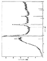
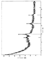
従来の相変化記憶材料であるGeSb2Te4およびGeAsSbTe4に関するX線回折データが、それぞれ、図4および図5に示されている。これらの膜の結晶化したものにおける相は立方晶系である。これは、3.5、3.1、2.1および1.7Å近くの格子面間隔(d-spacing)値でのたった4つのピークの存在から推論される。これは、いわゆる「岩塩」またはNaCl構造の特徴を示している。 X-ray diffraction data for the conventional phase change memory materials GeSb 2 Te 4 and GeAsSbTe 4 are shown in FIGS. 4 and 5, respectively. The phase in the crystallized version of these films is cubic. This is inferred from the presence of only 4 peaks with d-spacing values near 3.5, 3.1, 2.1 and 1.7 Å. This is characteristic of the so-called “rock salt” or NaCl structure.
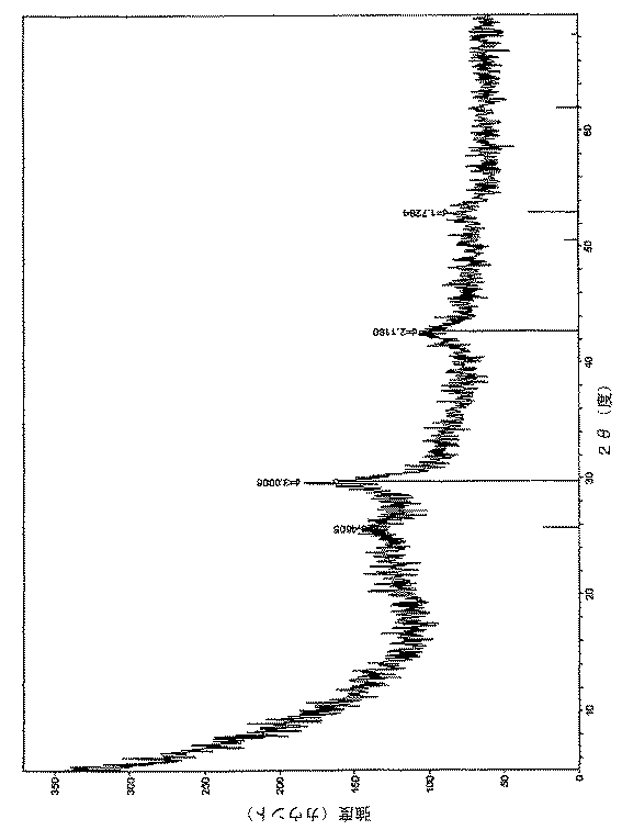
本発明による材料であるGeAs2Te4およびGeAs1.9Bi0.1Te4に関するX線回折データが、それぞれ、図6および図7に示されている。立方晶材料と比べて増加したピークの数は、本発明による材料が六方晶結晶相を含むことを示している。表1に示された追加の組成物のX線回折データが、六方晶結晶相と一致するピークを有することが分かった。 X-ray diffraction data for GeAs 2 Te 4 and GeAs 1.9 Bi 0.1 Te 4, materials according to the present invention, are shown in FIGS. 6 and 7, respectively. The increased number of peaks compared to the cubic material indicates that the material according to the invention contains a hexagonal crystal phase. It was found that the X-ray diffraction data for the additional compositions shown in Table 1 had a peak consistent with the hexagonal crystal phase.
さらなるGe14.3As28.6Te57.1薄膜物品を1から10分間に及ぶ時間に亘り空気中において350℃で加熱した。これらの物品に関する反射率データが図3に示されている。増加した反射率が、それぞれ、線28、30、および32により示される、1分間、5分間、および10分間に亘り加熱された物品に対する、線26により示される堆積されたままの物品から明白であった。
Additional Ge 14.3 As 28.6 Te 57.1 thin film articles were heated at 350 ° C. in air for a period ranging from 1 to 10 minutes. Reflectance data for these articles is shown in FIG. The increased reflectivity is evident from the as-deposited article indicated by
この方法を、表1に記載された組成物について繰り返し、同様の結果が得られた。As2Te3−GeTe接合線上の組成を有するサンプル由来の他の薄膜、並びに、原子パーセントで表される以下の近似組成範囲:5〜45%のGe、5〜40%のAs、および5〜65%のTeの範囲内の他のGeAsTeガラス、およびAl,Si,Ga,Se,In,Sn,Tl,Pb,Bi,P,S,またはそれらの組合せをさらに含む組成物についても、同様の結果が予測される。これらの追加の変更は、これらの材料の相変化特徴を低下させないべきである。 This method was repeated for the compositions described in Table 1 with similar results. Other thin films from samples with compositions on the As 2 Te 3 -GeTe junction line, and the following approximate composition ranges expressed in atomic percent: 5-45% Ge, 5-40% As, and 5-5 Similar for other GeAsTe glasses within the range of 65% Te and compositions further comprising Al, Si, Ga, Se, In, Sn, Tl, Pb, Bi, P, S, or combinations thereof Results are expected. These additional changes should not degrade the phase change characteristics of these materials.
本発明の精神すなわち範囲から逸脱せずに本発明に様々な改変および変更を行えることが当業者には明白であろう。それゆえ、本発明は、本発明の改変および変更を、それらが添付の特許請求の範囲およびそれらの同等物の範囲に含まれるという条件で包含することが意図されている。 It will be apparent to those skilled in the art that various modifications and variations can be made to the present invention without departing from the spirit or scope of the invention. Therefore, it is intended that the present invention cover modifications and variations of this invention provided they come within the scope of the appended claims and their equivalents.
以下、本願発明に係る物品の実施態様を記載する。 Hereinafter, embodiments of the article according to the present invention will be described.
実施態様1
a. 少なくとも1つの六方晶結晶相を有する組成物からなる結晶化薄膜、または
b. 結晶化形態で少なくとも1つの六方晶相を有することのできる結晶化可能な組成物、
を備えた物品であって、
前記組成物が、原子パーセントで表して、
5から45のGe、
5から40のAs、またはAsとSbの組合せ、ここで、Asの原子パーセントはSbの原子パーセントよりも大きい、
45から65のTe、および
Al,Si,Ga,Se,In,Sn,Tl,Pb,Bi,P,S,またはそれらの組合せを含むものである、物品。
Embodiment 1
a. A crystallized thin film comprising a composition having at least one hexagonal crystal phase, or b. A crystallizable composition capable of having at least one hexagonal phase in crystallized form;
An article comprising
Wherein the composition is expressed in atomic percent;
5 to 45 Ge,
5 to 40 As, or a combination of As and Sb, where the atomic percent of As is greater than the atomic percent of Sb;
Articles comprising 45 to 65 Te and Al, Si, Ga, Se, In, Sn, Tl, Pb, Bi, P, S, or combinations thereof.
実施態様2
前記Al,Si,Ga,Se,In,Sn,Tl,Pb,Bi,P,S,またはそれらの組合せの原子パーセントが20パーセント以下であることを特徴とする実施態様1記載の物品。
The article of embodiment 1, wherein the atomic percent of the Al, Si, Ga, Se, In, Sn, Tl, Pb, Bi, P, S, or combinations thereof is 20 percent or less.
実施態様3
前記薄膜が基板上に配置されることを特徴とする実施態様1または2記載の物品。
Embodiment 3
3. An article according to
Claims (2)
該相変化記憶非晶性材料を六方晶結晶相に転化させる、
各工程を有してなり、
前記相変化記憶非晶性材料は、原子パーセントで表して、
5から45のGe、
5から40のAs、またはAsとSbの組合せ、ここで、Asの原子パーセントはSbの原子パーセントよりも大きい、
45から65のTe、および
Al,Si,Ga,Se,In,Sn,Tl,Pb,Bi,P,S,またはそれらの組合せを含むものである、
方法。 A thin film of phase change memory amorphous material is deposited on a substrate by pulsed laser deposition,
Converting the phase change memory amorphous material into a hexagonal crystalline phase;
Having each process,
The phase change memory amorphous material is expressed in atomic percent,
5 to 45 Ge,
5 to 40 As, or a combination of As and Sb, where the atomic percent of As is greater than the atomic percent of Sb;
45 to 65 Te, and Al, Si, Ga, Se, In, Sn, Tl, Pb, Bi, P, S, or combinations thereof,
Method.
該六方晶結晶相を非晶相に転化させる、
各工程を有してなり、
前記相変化記憶材料は、原子パーセントで表して、
5から45のGe、
5から40のAs、またはAsとSbの組合せ、ここで、Asの原子パーセントはSbの原子パーセントよりも大きい、
45から65のTe、および
Al,Si,Ga,Se,In,Sn,Tl,Pb,Bi,P,S,またはそれらの組合せを含むものである、
方法。 A thin film made of a phase change memory material having a hexagonal crystal phase is deposited on a substrate by pulsed laser deposition,
Converting the hexagonal crystal phase to an amorphous phase;
Having each process,
The phase change memory material is expressed in atomic percent,
5 to 45 Ge,
5 to 40 As, or a combination of As and Sb, where the atomic percent of As is greater than the atomic percent of Sb;
45 to 65 Te, and Al, Si, Ga, Se, In, Sn, Tl, Pb, Bi, P, S, or combinations thereof,
Method.
Applications Claiming Priority (4)
| Application Number | Priority Date | Filing Date | Title |
|---|---|---|---|
| US9286808P | 2008-08-29 | 2008-08-29 | |
| US61/092,868 | 2008-08-29 | ||
| US12/503,156 US8206804B2 (en) | 2008-08-29 | 2009-07-15 | Phase change memory materials |
| US12/503,156 | 2009-07-15 |
Related Parent Applications (1)
| Application Number | Title | Priority Date | Filing Date |
|---|---|---|---|
| JP2011525009A Division JP2012501511A (en) | 2008-08-29 | 2009-08-28 | Phase change memory material |
Publications (2)
| Publication Number | Publication Date |
|---|---|
| JP2015018596A true JP2015018596A (en) | 2015-01-29 |
| JP6053041B2 JP6053041B2 (en) | 2016-12-27 |
Family
ID=41507809
Family Applications (2)
| Application Number | Title | Priority Date | Filing Date |
|---|---|---|---|
| JP2011525009A Pending JP2012501511A (en) | 2008-08-29 | 2009-08-28 | Phase change memory material |
| JP2014146705A Expired - Fee Related JP6053041B2 (en) | 2008-08-29 | 2014-07-17 | Phase change memory material |
Family Applications Before (1)
| Application Number | Title | Priority Date | Filing Date |
|---|---|---|---|
| JP2011525009A Pending JP2012501511A (en) | 2008-08-29 | 2009-08-28 | Phase change memory material |
Country Status (7)
| Country | Link |
|---|---|
| US (1) | US8206804B2 (en) |
| EP (1) | EP2335297A1 (en) |
| JP (2) | JP2012501511A (en) |
| KR (1) | KR101715956B1 (en) |
| CN (1) | CN102138233B (en) |
| TW (1) | TWI404633B (en) |
| WO (1) | WO2010024936A1 (en) |
Families Citing this family (3)
| Publication number | Priority date | Publication date | Assignee | Title |
|---|---|---|---|---|
| US10889887B2 (en) | 2016-08-22 | 2021-01-12 | Honeywell International Inc. | Chalcogenide sputtering target and method of making the same |
| CN106601907B (en) * | 2016-12-14 | 2019-02-22 | 中国科学院上海微系统与信息技术研究所 | A kind of gating tube material, gating pipe unit and preparation method thereof |
| CN109880451B (en) * | 2019-01-18 | 2020-12-18 | 申再军 | Ceramic coating material based on phase change, wall thermal insulation material and preparation method thereof |
Citations (3)
| Publication number | Priority date | Publication date | Assignee | Title |
|---|---|---|---|---|
| WO1991005342A1 (en) * | 1989-09-28 | 1991-04-18 | Matsushita Electric Industrial Co., Ltd. | Optical data recording medium and method of producing the same |
| JPH0562239A (en) * | 1991-06-20 | 1993-03-12 | Hitachi Ltd | Recording medium and information recording method by using this medium |
| JP2008103053A (en) * | 2006-03-13 | 2008-05-01 | Ricoh Co Ltd | Optical recording medium |
Family Cites Families (10)
| Publication number | Priority date | Publication date | Assignee | Title |
|---|---|---|---|---|
| DE60030493T2 (en) * | 1999-05-19 | 2007-05-03 | Mitsubishi Kagaku Media Co., Ltd. | Optical recording medium and recording method |
| US20020160305A1 (en) * | 2001-03-08 | 2002-10-31 | Mitsubishi Chemical Corporation | Optical recording medium, method of writing and erasing information using the same, and process of producing the same |
| JP2003200665A (en) * | 2001-03-08 | 2003-07-15 | Mitsubishi Chemicals Corp | Medium for optical information recording, method for erasing its recording and method for manufacturing it |
| US6930913B2 (en) | 2002-02-20 | 2005-08-16 | Stmicroelectronics S.R.L. | Contact structure, phase change memory cell, and manufacturing method thereof with elimination of double contacts |
| TWI226058B (en) * | 2002-09-11 | 2005-01-01 | Tdk Corp | Optical recording medium |
| KR100651657B1 (en) * | 2005-06-29 | 2006-12-01 | 한국과학기술연구원 | Phase change material for high density non-volatile memory |
| US8188454B2 (en) * | 2005-10-28 | 2012-05-29 | Ovonyx, Inc. | Forming a phase change memory with an ovonic threshold switch |
| US7626190B2 (en) * | 2006-06-02 | 2009-12-01 | Infineon Technologies Ag | Memory device, in particular phase change random access memory device with transistor, and method for fabricating a memory device |
| KR20080055508A (en) * | 2006-12-15 | 2008-06-19 | 삼성전자주식회사 | Phase change layer having different crystal lattice in single layer and method of forming the same and phase change memory device comprising means for preventing ti diffusion and method of manufacturing the same |
| KR20090002506A (en) * | 2007-06-29 | 2009-01-09 | 제일모직주식회사 | Cmp slurry composition for the phase change memory materials and polishing method using the same |
-
2009
- 2009-07-15 US US12/503,156 patent/US8206804B2/en not_active Expired - Fee Related
- 2009-08-28 TW TW98129195A patent/TWI404633B/en not_active IP Right Cessation
- 2009-08-28 EP EP09789238A patent/EP2335297A1/en not_active Withdrawn
- 2009-08-28 JP JP2011525009A patent/JP2012501511A/en active Pending
- 2009-08-28 WO PCT/US2009/004922 patent/WO2010024936A1/en active Application Filing
- 2009-08-28 CN CN200980134692.6A patent/CN102138233B/en not_active Expired - Fee Related
- 2009-08-28 KR KR1020117007093A patent/KR101715956B1/en active IP Right Grant
-
2014
- 2014-07-17 JP JP2014146705A patent/JP6053041B2/en not_active Expired - Fee Related
Patent Citations (3)
| Publication number | Priority date | Publication date | Assignee | Title |
|---|---|---|---|---|
| WO1991005342A1 (en) * | 1989-09-28 | 1991-04-18 | Matsushita Electric Industrial Co., Ltd. | Optical data recording medium and method of producing the same |
| JPH0562239A (en) * | 1991-06-20 | 1993-03-12 | Hitachi Ltd | Recording medium and information recording method by using this medium |
| JP2008103053A (en) * | 2006-03-13 | 2008-05-01 | Ricoh Co Ltd | Optical recording medium |
Non-Patent Citations (1)
| Title |
|---|
| JPN5011012568; MOHAMED S H: 'STRUCTURAL AND OPTICAL PROPERTIES OF GE-AS-TE THIN FILMS' EUROPEAN PHYSICAL JOURNAL V34 N3, 200606, P165-171, APPLIED PHYSICS EDP SCIENCES * |
Also Published As
| Publication number | Publication date |
|---|---|
| EP2335297A1 (en) | 2011-06-22 |
| US8206804B2 (en) | 2012-06-26 |
| JP6053041B2 (en) | 2016-12-27 |
| KR20110059732A (en) | 2011-06-03 |
| JP2012501511A (en) | 2012-01-19 |
| TW201026504A (en) | 2010-07-16 |
| CN102138233A (en) | 2011-07-27 |
| US20100055493A1 (en) | 2010-03-04 |
| TWI404633B (en) | 2013-08-11 |
| KR101715956B1 (en) | 2017-03-13 |
| WO2010024936A1 (en) | 2010-03-04 |
| CN102138233B (en) | 2014-07-02 |
Similar Documents
| Publication | Publication Date | Title |
|---|---|---|
| EP0499273B1 (en) | Congruent state changeable optical memory alloy and data carrier | |
| Raoux et al. | Phase change materials and their application to random access memory technology | |
| US6723410B2 (en) | Optical recording medium | |
| Singh et al. | Electrical, optical, and thermal properties of Sn-doped phase change material Ge 2 Sb 2 Te 5 | |
| JP6053041B2 (en) | Phase change memory material | |
| TW487682B (en) | Rewritable phase-change type optical information recording composition and optical disk containing the same | |
| Lie et al. | Ge2Sb2Te5 thin film doped with silver | |
| JP3899770B2 (en) | Optical information recording medium, reproducing method and recording method thereof | |
| KR20080016120A (en) | Phase change memory device and fabrication methods of using the same | |
| WO2023008432A1 (en) | Phase change material | |
| JPH10112028A (en) | Optical information recording medium | |
| Yamada | Development of materials for third generation optical storage media | |
| TW479257B (en) | Rewritable optical information medium | |
| JP2006164484A (en) | Write-once optical recording medium | |
| JP2781421B2 (en) | Manufacturing method of optical recording medium | |
| KR100411336B1 (en) | Phase change optical recording material for rewritable optical recording medium | |
| WO2023012930A1 (en) | Phase change material and phase change memory element | |
| US6753059B2 (en) | Optical recording material and optical recording medium using same | |
| JP2766276B2 (en) | Rewritable phase-change optical memory medium | |
| TW554339B (en) | Optical information recording medium | |
| Mongia et al. | Crystallization kinetics in (AgSbTe) x (In 1− y Sb y) 1− x films used in optical data storage | |
| Matsushita et al. | Effect of Sb, Te, and Ge addition on optical recording films with Ge2Sb2Te5 composition | |
| Zhu et al. | Research on phase-change of disc recording media GaSbBi | |
| TW200809844A (en) | Optical recording medium | |
| Jones | Phase change memory materials: Why do Ge/Sb/Te alloys dominate |
Legal Events
| Date | Code | Title | Description |
|---|---|---|---|
| A977 | Report on retrieval |
Free format text: JAPANESE INTERMEDIATE CODE: A971007 Effective date: 20151119 |
|
| A131 | Notification of reasons for refusal |
Free format text: JAPANESE INTERMEDIATE CODE: A131 Effective date: 20151124 |
|
| A601 | Written request for extension of time |
Free format text: JAPANESE INTERMEDIATE CODE: A601 Effective date: 20160222 |
|
| A601 | Written request for extension of time |
Free format text: JAPANESE INTERMEDIATE CODE: A601 Effective date: 20160311 |
|
| A521 | Request for written amendment filed |
Free format text: JAPANESE INTERMEDIATE CODE: A523 Effective date: 20160511 |
|
| TRDD | Decision of grant or rejection written | ||
| A01 | Written decision to grant a patent or to grant a registration (utility model) |
Free format text: JAPANESE INTERMEDIATE CODE: A01 Effective date: 20161101 |
|
| A61 | First payment of annual fees (during grant procedure) |
Free format text: JAPANESE INTERMEDIATE CODE: A61 Effective date: 20161125 |
|
| R150 | Certificate of patent or registration of utility model |
Ref document number: 6053041 Country of ref document: JP Free format text: JAPANESE INTERMEDIATE CODE: R150 |
|
| LAPS | Cancellation because of no payment of annual fees |