JP2014530581A - Lens stack array including adaptive optics - Google Patents
Lens stack array including adaptive optics Download PDFInfo
- Publication number
- JP2014530581A JP2014530581A JP2014535886A JP2014535886A JP2014530581A JP 2014530581 A JP2014530581 A JP 2014530581A JP 2014535886 A JP2014535886 A JP 2014535886A JP 2014535886 A JP2014535886 A JP 2014535886A JP 2014530581 A JP2014530581 A JP 2014530581A
- Authority
- JP
- Japan
- Prior art keywords
- lens stack
- adaptive optical
- optical element
- array
- camera module
- Prior art date
- Legal status (The legal status is an assumption and is not a legal conclusion. Google has not performed a legal analysis and makes no representation as to the accuracy of the status listed.)
- Pending
Links
Images


Classifications
-
- H—ELECTRICITY
- H04—ELECTRIC COMMUNICATION TECHNIQUE
- H04N—PICTORIAL COMMUNICATION, e.g. TELEVISION
- H04N23/00—Cameras or camera modules comprising electronic image sensors; Control thereof
- H04N23/45—Cameras or camera modules comprising electronic image sensors; Control thereof for generating image signals from two or more image sensors being of different type or operating in different modes, e.g. with a CMOS sensor for moving images in combination with a charge-coupled device [CCD] for still images
-
- H—ELECTRICITY
- H04—ELECTRIC COMMUNICATION TECHNIQUE
- H04N—PICTORIAL COMMUNICATION, e.g. TELEVISION
- H04N23/00—Cameras or camera modules comprising electronic image sensors; Control thereof
- H04N23/60—Control of cameras or camera modules
- H04N23/67—Focus control based on electronic image sensor signals
-
- G—PHYSICS
- G02—OPTICS
- G02B—OPTICAL ELEMENTS, SYSTEMS OR APPARATUS
- G02B3/00—Simple or compound lenses
- G02B3/0006—Arrays
-
- H—ELECTRICITY
- H04—ELECTRIC COMMUNICATION TECHNIQUE
- H04N—PICTORIAL COMMUNICATION, e.g. TELEVISION
- H04N23/00—Cameras or camera modules comprising electronic image sensors; Control thereof
- H04N23/95—Computational photography systems, e.g. light-field imaging systems
- H04N23/958—Computational photography systems, e.g. light-field imaging systems for extended depth of field imaging
- H04N23/959—Computational photography systems, e.g. light-field imaging systems for extended depth of field imaging by adjusting depth of field during image capture, e.g. maximising or setting range based on scene characteristics
Landscapes
- Engineering & Computer Science (AREA)
- Multimedia (AREA)
- Signal Processing (AREA)
- Physics & Mathematics (AREA)
- Computing Systems (AREA)
- Theoretical Computer Science (AREA)
- General Physics & Mathematics (AREA)
- Optics & Photonics (AREA)
- Human Computer Interaction (AREA)
- Studio Devices (AREA)
- Liquid Crystal (AREA)
Abstract
本発明の実施形態による、システムおよび方法は、適応光学要素をレンズスタックアレイ内の光学チャネルに組み込む。一実施形態では、アレイカメラモジュールは、少なくとも2つのレンズスタックを含む、レンズスタックアレイであって、少なくとも1つのレンズスタックは、少なくとも1つの電気信号に応答して、対応するレンズスタックによって画定される光学チャネル内の光の透過の特性を調節することができる、適応光学要素を含む、アレイと、レンズスタックアレイ内の各レンズスタックのための焦点面を含む、センサと、少なくとも1つの適応光学要素を制御するように構成される、回路とを含み、レンズスタックアレイおよびセンサは、各レンズスタックが、対応する焦点面上に像を形成することができるように構成される。Systems and methods according to embodiments of the present invention incorporate adaptive optical elements into optical channels within a lens stack array. In one embodiment, the array camera module is a lens stack array that includes at least two lens stacks, wherein the at least one lens stack is defined by a corresponding lens stack in response to at least one electrical signal. At least one adaptive optical element including an array including adaptive optical elements, a focal plane for each lens stack in the lens stack array, wherein the optical transmission characteristics in the optical channel can be adjusted A lens stack array and a sensor configured to allow each lens stack to form an image on a corresponding focal plane.
Description
本発明は、レンズスタックアレイに関し、より具体的には、適応光学要素を含む、レンズスタックアレイに関する。 The present invention relates to lens stack arrays, and more particularly to lens stack arrays that include adaptive optical elements.
暗箱に基づく従来のデジタルカメラに課される制約に応じて、アレイカメラと称され得る、新しい種類のカメラが、提案されている。アレイカメラは、ピクセルの複数のアレイを含み、各ピクセルアレイが、典型的には、焦点面(焦点面は、代替として、「焦点面アレイ」とも称され得る)を画定するように意図され、各焦点面が、典型的には、別個のレンズシステムと関連付けられることを特徴とする。多くの事例では、アレイカメラは、複数の焦点面およびレンズスタックアレイを組み込むセンサを使用して、構築される。各レンズスタックは、典型的には、1つ以上のレンズと、(限定されないが)絞り、フィルタ、基板、および(不透明)スペーサを含む、付加的構成要素とを含む。 Depending on the constraints imposed on conventional digital cameras based on dark boxes, a new type of camera has been proposed that can be referred to as an array camera. An array camera includes a plurality of arrays of pixels, each pixel array typically intended to define a focal plane (the focal plane may alternatively be referred to as a “focal plane array”), Each focal plane is typically characterized by being associated with a separate lens system. In many cases, an array camera is built using sensors that incorporate multiple focal planes and a lens stack array. Each lens stack typically includes one or more lenses and additional components including (but not limited to) an aperture, a filter, a substrate, and (opaque) spacers.
本発明の実施形態による、システムおよび方法は、適応光学要素をレンズスタックアレイ内の光学チャネルに組み込む。一実施形態によると、アレイカメラモジュールは、少なくとも2つのレンズスタックを含む、レンズスタックアレイであって、少なくとも1つのレンズスタックは、少なくとも1つの電気信号に応答して、対応するレンズスタックによって画定される光学チャネル内の光の透過の特性を調節することができる、適応光学要素を含む、アレイと、レンズスタックアレイ内の各レンズスタックのための焦点面を含む、センサであって、各焦点面は、また、複数のピクセル列を形成する、複数のピクセル行を備え、各焦点面は、別の焦点面からのピクセルを含有しない、センサの領域内に含有される、センサと、少なくとも1つの適応光学要素を制御するように構成される、回路とを含み、レンズスタックアレイおよびセンサは、各レンズスタックが、対応する焦点面上に像を形成することができるように構成される。 Systems and methods according to embodiments of the present invention incorporate adaptive optical elements into optical channels in a lens stack array. According to one embodiment, the array camera module is a lens stack array that includes at least two lens stacks, wherein the at least one lens stack is defined by a corresponding lens stack in response to at least one electrical signal. A sensor including an adaptive optical element and a focal plane for each lens stack in the lens stack array, wherein the focal plane for each lens stack in the lens stack array can be adjusted. Also comprising a plurality of pixel rows forming a plurality of pixel columns, each focal plane containing no pixels from another focal plane, contained in the area of the sensor, and at least one A lens stack array and a sensor configured to control the adaptive optical element, wherein each lens stack Configured to be able to form an image on the corresponding focal plane.
別の実施形態では、アレイカメラモジュールはさらに、センサによって発生される少なくとも1つの電気信号に基づいて、少なくとも1つの適応光学要素を制御するための回路を含む。 In another embodiment, the array camera module further includes circuitry for controlling at least one adaptive optical element based on at least one electrical signal generated by the sensor.
なおも別の実施形態では、レンズスタックアレイ内のレンズスタックはそれぞれ、少なくとも1つの適応光学要素を含む。 In yet another embodiment, each lens stack in the lens stack array includes at least one adaptive optical element.
別の実施形態では、適応光学要素のうちの少なくとも1つは、その対応するレンズスタックの焦点距離を調節するように構成される。 In another embodiment, at least one of the adaptive optical elements is configured to adjust the focal length of its corresponding lens stack.
さらに別の実施形態では、少なくとも1つの適応光学要素は、その焦点距離が、その対応する焦点面と整合されるように、その対応するレンズスタックの焦点距離を調節するように構成される。 In yet another embodiment, the at least one adaptive optical element is configured to adjust the focal length of its corresponding lens stack such that its focal length is aligned with its corresponding focal plane.
さらなる実施形態では、その対応するレンズスタックの焦点距離を調節するように構成される、少なくとも1つの適応光学要素は、少なくとも1つの圧電要素を含み、少なくとも1つの圧電要素の起動が、適応光学要素に、その対応するレンズスタックの焦点距離を調節させる。 In a further embodiment, the at least one adaptive optical element configured to adjust the focal length of its corresponding lens stack includes at least one piezoelectric element, and activation of the at least one piezoelectric element is The focal length of the corresponding lens stack is adjusted.
さらに別の実施形態では、その対応するレンズスタックの焦点距離を調節するように構成される、少なくとも1つの適応光学要素はまた、ガラス支持体、ポリマー層、および薄ガラス膜を含み、ガラス支持体は、ポリマー層の片側に隣接して配置され、薄ガラス膜は、ポリマー層の第2の反対側に隣接して配置され、少なくとも1つの圧電要素は、圧電要素の起動が、対応するレンズスタックの焦点距離が制御可能に調節されるよう、薄ガラス膜を偏向させるように、ガラス膜に結合される。 In yet another embodiment, the at least one adaptive optical element configured to adjust the focal length of its corresponding lens stack also includes a glass support, a polymer layer, and a thin glass film, the glass support Is disposed adjacent to one side of the polymer layer, the thin glass film is disposed adjacent to the second opposite side of the polymer layer, and at least one piezoelectric element has a corresponding lens stack upon activation of the piezoelectric element. Is coupled to the glass film to deflect the thin glass film such that the focal length of the glass film is controllably adjusted.
別の実施形態では、適応光学要素は、液晶要素を含む、液晶層を含む。 In another embodiment, the adaptive optical element includes a liquid crystal layer that includes a liquid crystal element.
なおも別の実施形態では、適応光学要素はまた、第1のガラス基板、第2のガラス基板、第3のガラス基板、第1の電極、第2の電極、および成形層を含み、成形層は、同一の屈折率であるが、異なる誘電特性を有する、2つの異なる材料を含み、第1の電極は、第1のガラス基板と液晶層との間に隣接し、かつその中に配置され、液晶層は、第1の電極と第2のガラス基板との間に隣接し、かつその中に配置され、第2のガラス基板は、液晶層と成形層との間に隣接し、かつその中に配置され、成形層は、第2のガラス基板と第2の電極との間に隣接し、かつその中に配置され、第2の電極は、成形層および第3のガラス基板との間に隣接し、かつその中に配置され、電位差が、第1の電極および第2の電極にわたって印加されると、電位差は、レンズスタックの焦点距離を調節するように、液晶要素の差動回転を生じさせる。 In yet another embodiment, the adaptive optical element also includes a first glass substrate, a second glass substrate, a third glass substrate, a first electrode, a second electrode, and a molding layer, wherein the molding layer Includes two different materials having the same refractive index but different dielectric properties, and the first electrode is adjacent to and disposed within the first glass substrate and the liquid crystal layer. The liquid crystal layer is adjacent to and disposed within the first electrode and the second glass substrate, and the second glass substrate is adjacent to and between the liquid crystal layer and the molding layer; and And the molding layer is disposed adjacent to and between the second glass substrate and the second electrode, and the second electrode is disposed between the molding layer and the third glass substrate. The potential difference is applied across the first electrode and the second electrode. So as to adjust the focal length of the lens stack, causing differential rotation of the liquid crystal element.
別の実施形態では、適応光学要素は、電場を発生するように構成される、複数の電極を含み、その規模は、対応するレンズスタックに対する半径方向位置の関数として変動する。 In another embodiment, the adaptive optical element includes a plurality of electrodes configured to generate an electric field, the magnitude of which varies as a function of radial position relative to the corresponding lens stack.
さらに別の実施形態では、適応光学要素は、その厚さを変動させることによって、焦点距離を調節するように構成される。 In yet another embodiment, the adaptive optical element is configured to adjust the focal length by varying its thickness.
なおも別の実施形態では、適応光学要素は、個別のレンズスタック内の少なくとも1つのレンズ要素の軸方向位置を変動させることによって、像位置を調節するように構成される。 In yet another embodiment, the adaptive optical element is configured to adjust the image position by varying the axial position of at least one lens element in the individual lens stack.
別の実施形態では、適応光学要素は、個別のスタック内の少なくとも1つのレンズ要素の軸方向位置を変動させるために、少なくとも1つのMEMSベースのアクチュエータを含む。 In another embodiment, the adaptive optical element includes at least one MEMS-based actuator to vary the axial position of at least one lens element in a separate stack.
なおも別の実施形態では、適応光学要素はさらに、像を拡大するように構成される。 In yet another embodiment, the adaptive optical element is further configured to magnify the image.
さらに別の実施形態では、適応光学要素は、個別のレンズスタック内の少なくとも1つのレンズ要素の軸方向位置を変動させるために、少なくとも1つのVCMを含む。 In yet another embodiment, the adaptive optical element includes at least one VCM to vary the axial position of at least one lens element within the individual lens stack.
さらなる実施形態では、適応光学要素のうちの少なくとも1つは、その対応するレンズスタックの中心視野角を調節するように構成される。 In a further embodiment, at least one of the adaptive optical elements is configured to adjust the central viewing angle of its corresponding lens stack.
なおもさらなる実施形態では、少なくとも1つの適応光学要素は、焦点面によって提供される像多様性の角度サンプリングを増加させるように、その対応するレンズスタックの中心視野角を調節するように構成される。 In a still further embodiment, the at least one adaptive optical element is configured to adjust the central viewing angle of its corresponding lens stack so as to increase the angular sampling of image diversity provided by the focal plane. .
なおもさらなる実施形態では、少なくとも1つの適応光学要素は、適応光学要素の屈折力分布の焦点化を制御するように構成される、複数の電極を含む。 In still further embodiments, the at least one adaptive optical element includes a plurality of electrodes configured to control focusing of the refractive power distribution of the adaptive optical element.
なおも別の実施形態では、電極は、電位差が、選択的に、電極のサブセットにわたって印加され、それによって、適応光学要素の屈折力分布の焦点化を制御し得るように、方位角によってセグメント化されたパターンに配列される。 In yet another embodiment, the electrodes are segmented by azimuth so that a potential difference can be selectively applied across the subset of electrodes, thereby controlling the focusing of the optical power distribution of the adaptive optical element. Arranged in a pattern.
さらに別の実施形態では、中心視野角の調節の程度は、カメラに対する物体の距離に基づき、その像は、焦点面が、捕捉している。 In yet another embodiment, the degree of adjustment of the central viewing angle is based on the distance of the object relative to the camera, and the image is captured by the focal plane.
別の実施形態では、適応光学要素のうちの少なくとも1つは、色順応能力を提供するように構成される。 In another embodiment, at least one of the adaptive optical elements is configured to provide chromatic adaptation capability.
さらに別の実施形態では、少なくとも1つの適応光学要素は、色特異的合焦を提供するように構成される。 In yet another embodiment, the at least one adaptive optical element is configured to provide color specific focusing.
なおも別の実施形態では、適応光学要素は全て、色特異的合焦を提供し、特異的に合焦される色は、赤色、青色、または緑色のうちの1つであって、色特異的合焦を伴う、適応光学要素は、レンズスタックアレイ上にπフィルタ群を実装するように構成される。 In yet another embodiment, all adaptive optical elements provide color specific focusing, and the specifically focused color is one of red, blue, or green, and the color specific An adaptive optical element with focal focus is configured to implement a π filter group on the lens stack array.
別の実施形態では、アレイカメラモジュールは、少なくとも1つの物理的パラメータを測定するように構成される、少なくとも1つの測定デバイスを含み、回路は、測定デバイスによって測定された少なくとも1つの物理的パラメータに基づいて、少なくとも1つの適応光学要素を制御するように構成される。 In another embodiment, the array camera module includes at least one measurement device configured to measure at least one physical parameter, and the circuit is configured to measure at least one physical parameter measured by the measurement device. Based on, it is configured to control at least one adaptive optical element.
なおもさらに別の実施形態では、少なくとも1つの適応光学要素は、温度を測定し、温度測定を示す、少なくとも1つの電気信号を発生させるように構成される、少なくとも1つの測定デバイスを含み、回路は、少なくとも1つの測定デバイスによって発生される、温度測定値を示す、少なくとも1つの電気信号に基づいて、適応光学要素を制御するように構成される。 In still yet another embodiment, the at least one adaptive optical element includes at least one measurement device configured to measure temperature and generate at least one electrical signal indicative of the temperature measurement, the circuit Is configured to control the adaptive optical element based on at least one electrical signal indicative of a temperature measurement generated by the at least one measuring device.
さらなる実施形態では、回路は、コントローラによって発生される少なくとも1つの電気信号に基づいて、少なくとも1つの適応光学要素を制御するように構成される。 In a further embodiment, the circuit is configured to control at least one adaptive optical element based on at least one electrical signal generated by the controller.
別の実施形態では、アレイカメラモジュールは、少なくとも2つのレンズスタックを含む、レンズスタックアレイであって、各レンズスタックは、電気信号に応答して、対応するレンズスタックによって画定される光学チャネル内の光の透過の特性を調節することができる、適応光学要素を含み、各適応光学要素は、液晶層と、電場を発生させることができる、複数の電極であって、その規模は、レンズスタックの焦点距離および中心視野方向が調節されることができるように、レンズスタックに対する半径方向および円周方向位置の関数として変動する、電極とを含む、アレイと、レンズスタックアレイ内の各レンズスタックのための焦点面を含む、センサであって、各焦点面は、複数のピクセル列を形成する、複数のピクセル行を備え、各焦点面は、別の焦点面からのピクセルを含有しない、センサの領域内に含有される、センサと、センサによって発生される少なくとも1つの電気信号に基づいて、少なくとも1つの適応光学要素を制御するように構成される、回路とを含み、レンズスタックアレイおよびセンサは、各レンズスタックが、対応する焦点面上に像を形成することができるように構成される。 In another embodiment, the array camera module is a lens stack array that includes at least two lens stacks, each lens stack in an optical channel defined by a corresponding lens stack in response to an electrical signal. An adaptive optical element capable of adjusting the characteristics of light transmission, each adaptive optical element being a liquid crystal layer and a plurality of electrodes capable of generating an electric field, the scale of which is For each lens stack in the lens stack array, including an array, and electrodes that vary as a function of radial and circumferential position relative to the lens stack so that the focal length and central field direction can be adjusted Wherein each focal plane comprises a plurality of pixel rows forming a plurality of pixel columns; The focal plane controls the at least one adaptive optical element based on the sensor and at least one electrical signal generated by the sensor contained within the area of the sensor that does not contain pixels from another focal plane. The lens stack array and the sensor are configured such that each lens stack is capable of forming an image on a corresponding focal plane.
次に、図面を参照して、本発明の実施形態による、適応光学要素をレンズスタックアレイの光学チャネルに組み込むためのシステムおよび方法が、図示される。適応光学要素は、電気信号に応答して、光学チャネル内の光の透過の特性を調節することができる。米国特許出願第12/935,504号「Capturing and Processing of Images Using Monolithic Camera Array with Heterogeneous Imagers」では、Venkataraman et al.は、レンズスタックアレイを使用して、アレイカメラを構築するためのプロセスを説明している。米国特許出願第12/935,504号の開示は、参照することによって、全体として本明細書に組み込まれる。アレイカメラモジュールは、典型的には、アレイカメラモジュールの光学チャネル(対応するレンズスタックによって画定される光学チャネル)のそれぞれのための焦点面(すなわち、対応するレンズスタックによって、その上に形成される像を捕捉するように構成される、ピクセルのアレイ)を含む、モノリシックセンサと、レンズスタックアレイとが、各焦点面が各光学チャネル内のその対応するレンズスタックの焦点距離に位置付けられるように、相互に対して位置するような方法において構築されるように意図される。焦点面は、典型的には、また、複数のピクセル列を形成する、複数のピクセル行を含み、各焦点面は、典型的には、別の焦点面からのピクセルを含有しない、センサの領域内に含有される。レンズスタックアレイは、アレイ内の個々のレンズスタックが、相互に対して移動することができないように、剛性であってもよい。レンズスタックとその対応する焦点面の組み合わせは、「カメラモジュール」であると理解されることができる。 Referring now to the drawings, a system and method for incorporating adaptive optical elements into an optical channel of a lens stack array according to an embodiment of the present invention is illustrated. The adaptive optical element can adjust the characteristics of light transmission in the optical channel in response to the electrical signal. In US patent application Ser. No. 12 / 935,504, “Capturing and Processing of Images, Using Monolithic Camera Array with Heterogeneous Imagers,” Venkataramaman et al. Describes a process for building an array camera using a lens stack array. The disclosure of US patent application Ser. No. 12 / 935,504 is hereby incorporated by reference in its entirety. The array camera module is typically formed thereon by a focal plane (ie, a corresponding lens stack) for each of the optical channels (an optical channel defined by the corresponding lens stack) of the array camera module. An array of pixels configured to capture an image) and a lens stack array such that each focal plane is positioned at the focal length of its corresponding lens stack in each optical channel, It is intended to be constructed in such a way that they are located relative to each other. The focal plane typically includes a plurality of pixel rows that also form a plurality of pixel columns, each focal plane typically containing no pixels from another focal plane. Contained within. The lens stack array may be rigid so that the individual lens stacks in the array cannot move relative to each other. The combination of a lens stack and its corresponding focal plane can be understood as a “camera module”.
理想的には、アレイカメラのレンズスタックアレイは、各レンズスタックが、同一の焦点距離を有するように構築される。しかしながら、レンズスタックアレイの製造の際に伴われる多数の公差は、公称規定から逸脱する、焦点距離等のパラメータを有する、レンズスタックをもたらし得る。センサのモノリシック性質のため、典型的には、剛性レンズスタックアレイ内の各レンズスタックの焦点距離に対応する距離に設置されることができない。したがって、レンズスタック間の製造上のばらつきは、焦点がずれた光学チャネルによって形成される、像の一部または全部をもたらし得る。着目すべきこととして、これらの製造上のばらつきは、同一の製造プロセスから加工されたレンズスタックアレイ間でさえ、異なる焦点距離をもたらし得る。加えて、(限定されないが)スペーサ厚およびセンサに対するレンズスタックアレイの整合のばらつきを含む、アレイカメラモジュールのアセンブリと関連付けられた他の製造公差も、光学チャネルの全てに影響を及ぼし得る。 Ideally, the lens stack array of an array camera is constructed so that each lens stack has the same focal length. However, a number of tolerances involved in manufacturing a lens stack array can result in a lens stack having parameters such as focal length that deviate from the nominal specification. Due to the monolithic nature of the sensor, it cannot typically be placed at a distance corresponding to the focal length of each lens stack in the rigid lens stack array. Thus, manufacturing variations between lens stacks can result in some or all of the image formed by defocused optical channels. It should be noted that these manufacturing variations can result in different focal lengths even between lens stack arrays fabricated from the same manufacturing process. In addition, other manufacturing tolerances associated with the assembly of the array camera module, including (but not limited to) variations in spacer thickness and alignment of the lens stack array to the sensor, can also affect all of the optical channels.
米国仮特許出願第61/666,852号「Systems and Methods for Manufacturing Camera Modules Using Active Alignment of Lens Stack Arrays and Sensors」では、Duparre et al.は、レンズパラメータのばらつきからもたらされる悪影響を減少させるように、レンズスタックアレイとセンサの整合を含む、解決策を説明している。米国特許出願第61/666,852号の開示は、参照することによって、全体として本明細書に組み込まれる。 US Provisional Patent Application No. 61 / 666,852 “Systems and Methods for Manufacturing Camera Modules Using Active Alignment of Lens Stack Arrays and Sensors”, et al. Describe a solution that includes the alignment of the lens stack array and the sensor to reduce the adverse effects resulting from variations in lens parameters. The disclosure of US Patent Application No. 61 / 666,852 is hereby incorporated by reference in its entirety.
本発明の多くの実施形態では、レンズスタックアレイは、レンズスタックの焦点距離を修正することができる可変屈折力を伴う、適応光学要素を組み込むように利用される。適応光学要素を含む、レンズスタックアレイが、アレイカメラモジュールに組み込まれると、適応光学要素は、像距離が、レンズスタックとセンサ上の対応する焦点面との間の距離に対応するように、各レンズスタックの焦点距離を較正するように制御されることができる。いくつかの実施形態では、適応光学要素は、基準像を使用して、各光学チャネル内の焦点ずれを低減させるように較正される。適応光学要素のレンズスタック内への組み込みは、米国特許出願第61/666,852号に提供される解決策と比較して、レンズパラメータのばらつきからもたらされる悪影響を減少させるための費用効果的解決策を提供し得る。具体的には、適応光学レンズの組み込みは、米国特許出願第61/666,852号に開示されるもののように、厳密な能動的整合プロセスを採用する必要性をなくし得る。加えて、適応要素は、任意の整合プロセス(能動的整合プロセスを含む)を使用して製造される、カメラモジュール内で達成される結果を向上させることができる。 In many embodiments of the invention, the lens stack array is utilized to incorporate adaptive optical elements with variable refractive power that can modify the focal length of the lens stack. When a lens stack array, including adaptive optical elements, is incorporated into the array camera module, the adaptive optical elements are arranged so that the image distance corresponds to the distance between the lens stack and the corresponding focal plane on the sensor. It can be controlled to calibrate the focal length of the lens stack. In some embodiments, the adaptive optical element is calibrated to reduce defocus in each optical channel using the reference image. Incorporation of adaptive optics into the lens stack is a cost effective solution to reduce the negative effects resulting from lens parameter variations compared to the solution provided in US patent application Ser. No. 61 / 666,852. Can provide a solution. Specifically, the incorporation of adaptive optical lenses may eliminate the need to employ a strict active alignment process, such as that disclosed in US patent application Ser. No. 61 / 666,852. In addition, the adaptive element can improve the results achieved within the camera module that are manufactured using any alignment process (including an active alignment process).
さらに、適応光学要素は、適応光学要素の屈折力分布の焦点化を偏移させるために使用されることができる。このように、適応光学要素を利用して、センサ上の各焦点面によって捕捉される像間のサンプリング多様性を増加させることができる。Lelescu et al.の米国特許出願第12/967,807号「System and Methods for Synthesizing High Resolution Images Using Super−Resolution Processing」に開示されるように、サンプリング多様性の増加は、アレイカメラによって捕捉される複数の像から高解像度像を合成するとき、超解像(SR)処理を使用して達成される解像度の増加を改善することができる。米国特許出願第12/967,807号の開示は、参照することによって、全体として本明細書に組み込まれる。 Further, the adaptive optical element can be used to shift the focusing of the adaptive optical element's refractive power distribution. In this way, adaptive optics can be utilized to increase the sampling diversity between images captured by each focal plane on the sensor. Lelescu et al. As disclosed in US patent application Ser. No. 12 / 967,807, “Systems and Methods for Synthesizing High Resolution Images Using Super-Resolution Processing”, increased sampling diversity is captured by multiple images from an array camera. When compositing high resolution images, the resolution increase achieved using super-resolution (SR) processing can be improved. The disclosure of US patent application Ser. No. 12 / 967,807 is hereby incorporated by reference in its entirety.
いくつかの実施形態では、適応光学要素は、他の方法でレンズスタックを調節するために使用される。例えば、多くの実施形態では、適応光学要素を使用して、色順応を提供してもよい。いくつかの実施形態では、適応光学要素を使用して、光学スタックの温度のばらつきに対応してもよい。いくつかの実施形態では、暗電流測定を利用して、温度を測定し、適応光学要素が、適宜、変動される。 In some embodiments, adaptive optical elements are used to adjust the lens stack in other ways. For example, in many embodiments, adaptive optics may be used to provide chromatic adaptation. In some embodiments, adaptive optical elements may be used to accommodate optical stack temperature variations. In some embodiments, dark current measurement is utilized to measure temperature and the adaptive optical element is varied accordingly.
多数の実施形態では、場面の複数の像は、適応要素を使用して、レンズスタックのうちの1つ以上の焦点距離を調節しながら、高速で捕捉される。このように、プロセッサは、(限定されないが)より高い解像度像を合成するための超解像処理等の処理の施行に先立って、合焦を含むが、それらに限定されない、基準に従って、像を選択することができる。 In many embodiments, multiple images of the scene are captured at high speed while using adaptive elements to adjust the focal length of one or more of the lens stacks. In this way, the processor (without limitation) prior to performing a process such as super-resolution processing to synthesize a higher-resolution image, the image can be imaged according to criteria, including but not limited to focusing. You can choose.
本発明の実施形態による、アレイカメラ、レンズスタックアレイ、および適応光学要素は、以下にさらに論じられる。
(アレイカメラアーキテクチャ)
Array cameras, lens stack arrays, and adaptive optical elements according to embodiments of the present invention are discussed further below.
(Array camera architecture)
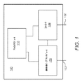
本発明の実施形態による、種々のアレイカメラ構成において使用され得る、アレイカメラアーキテクチャは、図1に図示される。アレイカメラ100は、像処理パイプラインモジュール120およびコントローラ130に接続される、アレイカメラモジュール110を含む。
An array camera architecture that can be used in various array camera configurations according to embodiments of the present invention is illustrated in FIG. The
アレイカメラモジュールは、2つ以上の焦点面を含み、それぞれ、別個のレンズスタックを通して、光を受光する。アレイカメラモジュールはまた、結像パラメータを制御するための他の回路と、物理的パラメータを測定し、対応する信号を発生させるための測定デバイスとを含むことができる。多くの実施形態では、アレイカメラモジュールは、アレイカメラモジュールの適応光学要素を制御するための回路を含む。いくつかの実施形態では、回路は、例えば、信号の発生および伝達を介して、デバイスと通信し、本通信に基づいて、適応光学要素を制御するように構成される。多数の実施形態では、回路は、センサと通信し、本通信に基づいて、適応光学要素を制御する。いくつかの実施形態では、回路は、コントローラと通信し、本通信に基づいて、適応光学要素を制御する。センサまたはコントローラは、測定デバイスによって発生された信号に基づいて、信号を回路に伝達してもよい。制御回路はまた、露光時間、利得、および黒色レベルオフセット等の結像パラメータを制御することができる。一実施形態では、結像パラメータを制御するための回路は、独立して、または同期様式において、各焦点面による像の捕捉をトリガしてもよい。アレイカメラモジュールは、動作温度における暗電流を推定するための暗ピクセルを含むが、それらに限定されない、種々の他の測定デバイスを含むことができる。本発明の実施形態による、アレイカメラにおいて利用され得る、アレイカメラモジュールは、Venkataraman et al.の米国特許出願第12/935,504号「Capturing and Processing of Images Using Monolithic Camera Array with Heterogeneous Imagers」に開示されている。 The array camera module includes two or more focal planes, each receiving light through a separate lens stack. The array camera module can also include other circuitry for controlling imaging parameters and a measuring device for measuring physical parameters and generating corresponding signals. In many embodiments, the array camera module includes circuitry for controlling adaptive optical elements of the array camera module. In some embodiments, the circuit is configured to communicate with the device, eg, via signal generation and transmission, and to control the adaptive optical element based on the communication. In many embodiments, the circuit communicates with the sensor and controls the adaptive optical element based on the communication. In some embodiments, the circuit communicates with the controller and controls the adaptive optical element based on the communication. The sensor or controller may communicate a signal to the circuit based on the signal generated by the measurement device. The control circuit can also control imaging parameters such as exposure time, gain, and black level offset. In one embodiment, a circuit for controlling imaging parameters may trigger image capture by each focal plane, either independently or in a synchronous manner. The array camera module can include a variety of other measurement devices including, but not limited to, dark pixels for estimating dark current at operating temperature. An array camera module that can be utilized in an array camera according to an embodiment of the present invention is described in Venkataraman et al. US patent application Ser. No. 12 / 935,504, “Capturing and Processing of Images Using Monolithic Camera Array with Heterogeneous Images”.
像処理パイプラインモジュール120は、アレイカメラモジュール110から受信した像を処理するためのハードウェア、ファームウェア、ソフトウェア、またはそれらの組み合わせである。像処理パイプラインモジュール120は、アレイカメラモジュール内の焦点面によって捕捉された複数の像を処理し、合成されたより高い解像度の像を生成する。いくつかの実施形態では、像処理パイプラインモジュール120は、出力122を介して、合成された像データを提供する。
The image
コントローラ130は、アレイカメラモジュール110の種々の動作パラメータを制御するためのハードウェア、ソフトウェア、ファームウェア、またはそれらの組み合わせである。コントローラ130は、入力132をユーザまたは他の外部構成要素から受信し、動作信号を送信し、アレイカメラモジュール110を制御する。コントローラ130はまた、情報を像処理パイプラインモジュール120に送信し、アレイカメラモジュール110内の焦点面によって捕捉された像の処理を補助することができる。
The
具体的アレイカメラアーキテクチャが、図1に図示されるが、像の捕捉および合成された高解像度像を生成するためのSRプロセスの適用を有効化する、代替アーキテクチャもまた、本発明の実施形態に従って、利用されることができる。本発明の実施形態による、アレイカメラモジュール内の適応光学要素の使用は、以下にさらに論じられる。
(アレイカメラモジュール)
Although a specific array camera architecture is illustrated in FIG. 1, alternative architectures that enable application of the SR process to capture images and generate a synthesized high resolution image are also in accordance with embodiments of the present invention. Can be utilized. The use of adaptive optical elements in an array camera module according to embodiments of the present invention is discussed further below.
(Array camera module)
本発明の多くの実施形態による、アレイカメラモジュールは、レンズスタックアレイと、焦点面のアレイを含む、モノリシックセンサの組み合わせを含む。レンズスタックアレイは、レンズスタックのアレイを含み、各レンズスタックは、別個の光学チャネルを画定する。レンズスタックアレイは、光学チャネルのそれぞれのための焦点面を含む、モノリシックセンサに搭載され、各焦点面は、像を捕捉するように構成される、ピクセルまたはセンサ要素のアレイを含む。レンズスタックアレイおよび焦点面のアレイを含むセンサが、十分な精度で組み合わせると、アレイカメラモジュールを利用して、場面の複数の像を捕捉することができ、これは、像処理パイプラインに渡され、SR処理を使用して、高解像度像を合成することができる。 An array camera module, according to many embodiments of the present invention, includes a combination of monolithic sensors, including a lens stack array and an array of focal planes. The lens stack array includes an array of lens stacks, each lens stack defining a separate optical channel. The lens stack array is mounted on a monolithic sensor that includes a focal plane for each of the optical channels, each focal plane including an array of pixels or sensor elements configured to capture an image. When a sensor including a lens stack array and an array of focal planes is combined with sufficient accuracy, an array camera module can be used to capture multiple images of the scene, which is passed to the image processing pipeline. SR processing can be used to synthesize high resolution images.
本発明のある実施形態による、レンズスタックアレイと、焦点面のアレイを含む、モノリシックセンサを組み合わせることによって形成される、アレイカメラモジュールの分解図は、図2に図示される。アレイカメラモジュール200は、レンズスタックアレイ210と、焦点面240のアレイを含む、センサ230とを含む。レンズスタックアレイ210は、レンズスタック220のアレイを含む。各レンズスタック220は、センサ230上の焦点面240のうちの1つ上の像を解像する、光学チャネルを作成する。レンズスタック220はそれぞれ、異なるタイプであってもよい。いくつかの実施形態では、光学チャネルを使用して、光スペクトルの波長の異なる部分の像を捕捉し、各光学チャネル内のレンズスタックは、光学チャネルと関連付けられた焦点面によって結像されたスペクトルの部分に特異的に最適化される。より具体的には、アレイカメラモジュールは、「πフィルタ群」でパターン化されてもよい。用語「πフィルタ群」とは、レンズスタックアレイまたはアレイカメラモジュールの焦点面に適用される色フィルタのパターンを指し、πフィルタ群でアレイカメラをパターン化するためのプロセスは、Venkataraman et al.による米国特許出願第61/641,164号「Camera Modules Patterned with π filter groups」に説明されている。米国特許出願第61/641,164号の開示は、参照することによって、全体として本明細書に組み込まれる。図3は、単一πフィルタ群を図示し、5つのカメラが、緑色光を受光するように構成され、2つのカメラが、赤色光を受光するように構成され、かつ2カメラは、青色光を受光するように構成される。
An exploded view of an array camera module formed by combining a monolithic sensor, including an array of lens stacks and an array of focal planes, in accordance with an embodiment of the present invention is illustrated in FIG. The
多くの実施形態では、アレイカメラモジュール230は、相互に対して軸方向に配列される1つまたは複数の別個の光学レンズ要素を有する、レンズスタック220を含む。以下にさらに論じられるように、本発明のいくつかの実施形態による、レンズスタックアレイ210は、各レンズスタックの焦点距離の独立調節および/または適応光学要素の屈折力分布の焦点化の後の偏移を有効化することができる、1つ以上の適応光学要素を含む。
In many embodiments, the
いくつかの実施形態では、アレイカメラモジュールは、ウエハレベル光学(WLO)技術を採用する。WLOは、例えば、レンズアレイをガラスウエハ上に成形し、適切なスペーサとともに、それらのウエハを積層(基板の両側に複製されるレンズを有する、ウエハを含む)した後、結像器とともに、直接、光学をモノリシック統合モジュール内にパッケージ化することを含む、いくつかのプロセスを包含する、技術である。 In some embodiments, the array camera module employs wafer level optics (WLO) technology. WLO, for example, molds a lens array on a glass wafer, stacks the wafers with appropriate spacers (including the wafers with lenses replicated on both sides of the substrate), and then directly with the imager A technology that encompasses several processes, including packaging optics into a monolithic integration module.
WLO手順は、他の手順の中でもとりわけ、ダイヤモンド切削加工を使用して、ガラス基板上に各プラスチックレンズ要素を作成することを伴い得る。より具体的には、WLOにおける、一連のプロセスは、概して、ダイヤモンド切削されたレンズマスタ(個々およびアレイレベルの両方において)を生成し、次いで、そのマスタの複製のためのネガ型鋳型(スタンプまたはツールとも呼ばれる)を生成し、次いで、最後に、例えば、開口(光遮断材料層内の透明開口部)等の適切な支持光学要素と、フィルタとともに構築される、ガラス基板上にポリマー複製物を形成することを含む。 The WLO procedure may involve creating each plastic lens element on a glass substrate using diamond cutting, among other procedures. More specifically, a series of processes in WLO generally produces a diamond-cut lens master (both at the individual and array level) and then a negative mold (stamp or (Also referred to as a tool) and then finally a polymer replica on a glass substrate built with a suitable supporting optical element such as an aperture (transparent aperture in the light blocking material layer) and a filter, for example. Forming.
WLOを使用したレンズスタックアレイの構築が、前述されているが、種々の技法のいずれも、レンズスタックアレイを構築するために使用されることができ、例えば、精密ガラス成形、ポリマー射出成形、またはウエハレベルポリマーモノリシックレンズプロセスを伴うものが挙げられる。本発明の実施形態による、適応光学要素を含む、レンズスタックアレイの構築は、以下にさらに論じられる。
(レンズスタックアレイ)
Although the construction of a lens stack array using WLO has been described above, any of a variety of techniques can be used to construct the lens stack array, such as precision glass molding, polymer injection molding, or One with a wafer level polymer monolithic lens process. The construction of a lens stack array, including adaptive optical elements, according to embodiments of the present invention is discussed further below.
(Lens stack array)
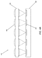
製造公差は、元々の規定から変動する、レンズスタックアレイの加工をもたらす。従来のレンズスタックアレイにおいて生じ得る、焦点距離のばらつきは、図4Aに概念的に図示される。アレイカメラモジュール400は、レンズスタックアレイ402を含み、レンズスタックは、センサ408の焦点面406上に光を合焦する。図示されるように、実際に加工されたレンズスタックとその元々の規定との間の相違は、若干、その規定から変動する、焦点距離を有し、その結果、レンズスタックアレイとセンサとの間の距離に一致しない、像距離を有する、レンズスタックをもたらし得る。故に、センサの焦点面上に形成される像は、焦点がずれ得る。本発明の多くの実施形態では、アレイカメラモジュールを利用して、像を捕捉し、これは、像処理パイプラインに提供され、SR処理を使用して、高解像度像を合成する。アレイカメラモジュールによって捕捉された像の焦点がずれると、SR処理を使用して達せされ得る、解像度利得の増加が、影響され得る。
Manufacturing tolerances result in processing of the lens stack array, which varies from the original definition. The focal length variation that can occur in a conventional lens stack array is conceptually illustrated in FIG. 4A. The
多数の実施形態では、場面の複数の像は、適応要素を使用して、レンズスタックのうちの1つ以上の焦点距離を調節しながら、高速で捕捉される。このように、プロセッサは、(限定されないが)より高い解像度像を合成するための超解像処理等の処理の施行に先立って、合焦を含むが、それらに限定されない、基準に従って、像を選択することができる。 In many embodiments, multiple images of the scene are captured at high speed while using adaptive elements to adjust the focal length of one or more of the lens stacks. In this way, the processor (without limitation) prior to performing a process such as super-resolution processing to synthesize a higher-resolution image, the image can be imaged according to criteria, including but not limited to focusing. You can choose.
本発明のいくつかの実施形態では、適応光学要素は、少なくとも1つのレンズスタックに組み込まれ、その個別の焦点距離の調節を有効化する。このように、適応光学要素の屈折力は、レンズスタックによって、センサ上の焦点面のアレイ上に形成される像の焦点ずれを低減させるように制御されることができる。レンズスタックアレイが、本発明のある実施形態による、適応光学要素を組み込む、アレイカメラモジュールは、図4Bに概念的に図示される。レンズスタックアレイ402’は、レンズスタック414’のそれぞれ内に、少なくとも1つの適応光学要素420を含む。適応光学要素の介入を伴わないレンズスタックのそれぞれの焦点距離は、破線を使用して示される。動作時、基準パターンは、光学チャネルのそれぞれ内の焦点ずれを判定するために利用されることができ、適切な制御が、適応光学要素に適用され、レンズスタックのそれぞれの焦点距離を修正することができる。
In some embodiments of the invention, the adaptive optical element is incorporated into at least one lens stack to enable adjustment of its individual focal length. In this way, the refractive power of the adaptive optical element can be controlled by the lens stack to reduce the defocus of the image formed on the array of focal planes on the sensor. An array camera module in which a lens stack array incorporates adaptive optical elements according to an embodiment of the present invention is conceptually illustrated in FIG. 4B. The lens stack array 402 'includes at least one adaptive
多くの実施形態では、適応光学要素は、その屈折力を制御可能に修正することができる、レンズスタック内の光学構成要素である。多数の実施形態では、屈折力を制御可能に修正することができる、適応光学要素は、個別のレンズスタック内の他の要素/レンズに対して、開口に最も近く、かつセンサから最も離れて、設置される。いくつかの実施形態では、適応光学要素の屈折力の修正は、(限定されないが)微小電気機械システム(MEMS)、能動的ポリマーアクチュエータ、および/または液体レンズを含め、機械的に達成される。いくつかの実施形態では、MEMSシステムは、ポリマーによって、ガラス支持体から分離される薄ガラス膜を備え、圧電要素が、力をガラス膜に印加する。いくつかの実施形態では、圧電要素は、ガラス膜が屈曲するように付勢し、光学電力変動を発生させる、圧電リングを含む。 In many embodiments, the adaptive optical element is an optical component in the lens stack that can controllably modify its refractive power. In many embodiments, the adaptive optical element, which can controllably modify the refractive power, is closest to the aperture and farthest from the sensor relative to other elements / lenses in the individual lens stack, Installed. In some embodiments, modification of the refractive power of the adaptive optical element is accomplished mechanically, including (but not limited to) a microelectromechanical system (MEMS), an active polymer actuator, and / or a liquid lens. In some embodiments, the MEMS system comprises a thin glass film that is separated from the glass support by a polymer, and the piezoelectric element applies a force to the glass film. In some embodiments, the piezoelectric element includes a piezoelectric ring that biases the glass film to bend and generate optical power fluctuations.
本発明のある実施形態による、薄ガラス膜、ポリマー、ガラス支持体、および圧電要素を備える、MEMSシステムは、図5Aおよび5Bに図示される。MEMSシステム500は、ガラス膜540を支持する、ポリマー520を支持する、ガラス支持体510を含む。ガラス膜は、圧電要素530に結合される。図5Aに示されるように、圧電要素530が、電圧に曝されていないとき、光線(破線によって示される)は、非摂動MEMSシステムを通過する。しかしながら、図5Bに示されるように、圧電要素530が起動されると、起動は、ガラス膜542を偏向させ、偏向は、MEMSシステムを通過する光線を倍増させ、それによって、焦点距離を調節する。圧電要素の起動の程度は、偏向の程度を制御し、これは、順に、焦点距離の調節と相関する。したがって、焦点距離は、圧電要素の起動の程度を制御することによって、操作されることができる。
A MEMS system comprising a thin glass film, a polymer, a glass support, and a piezoelectric element according to an embodiment of the invention is illustrated in FIGS. 5A and 5B. The
本発明のいくつかの実施形態では、適応光学要素の屈折力の修正は、限定されないが、成形された電場を印加し、液晶の層の屈折力を修正する、構成要素を含む、機械的に静的構成要素(すなわち、(肉眼的に)移動しない、構成要素)を使用して達成される。いくつかの実施形態では、液晶が、ガラス基板間に含有される、静的構成要素は、レンズスタックアレイの構築において利用され、ガラス基板は、レンズスタックアレイのさらなる複製のための基礎として利用される。 In some embodiments of the present invention, the modification of the optical power of the adaptive optical element includes, but is not limited to, a component that applies a shaped electric field and modifies the refractive power of the liquid crystal layer, including mechanical components. This is accomplished using static components (ie, components that do not move (visually)). In some embodiments, a liquid crystal is contained between the glass substrates, the static components are utilized in the construction of the lens stack array, and the glass substrate is utilized as a basis for further replication of the lens stack array. The
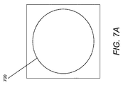
本発明のある実施形態による、レンズスタックアレイにおいて利用され得る、液晶適応光学要素は、図6に図示される。液晶適応光学要素600は、3つのガラス基板602、608、および614を含む。電極604は、第1のガラス基板602の内部表面上に形成され、液晶606の層は、電極と第2のガラス基板608との間に位置する。第2の電極612は、第3のガラス基板614の内部表面上に形成され、成形層610は、第2の電極612と第2のガラス基板608との間に位置する。図示される実施形態では、電極は、均一電場を発生させるように構成される。しかしながら、成形層は、同一の屈折率であるが、異なる誘電特性を有する、2つの異なる材料を含む。このように、成形層は、電極によって発生される均一電場を成形する。いくつかの実施形態では、成形層は、液晶層内で半径方向に変動する電場を作成し、液晶の半径方向に変動する配向をもたらす。成形層内の材料が、正しく構成/成形されると、電極に印加される単一電圧は、液晶要素の差動回転が、適応光学要素を通過する光を異なるように合焦させるよう変化され得るように制御されることができる。電極に印加される電圧を増加させることによって達成されることができる、屈折力の増加は、図7Aおよび7Bに概念的に図示される。図7Aに示される輪郭線700は、適応光学要素の屈折力分布を示し、適応光学要素の成形層内に異なる誘電特性を有する材料の円形対称形状のため、円形対称配列を有する。電極間の電圧が、増加されるにつれて(図7Bに示されるように)、輪郭線702の数は、増加し、屈折力の増加を示す。適応光学要素内の対の電極にわたる電圧を制御することによって、適切なレベルの屈折力が、達成されることができる。
A liquid crystal adaptive optical element that can be utilized in a lens stack array according to an embodiment of the invention is illustrated in FIG. The liquid crystal adaptive
本発明の実施形態による、適応光学要素の構成要素は、比較的により小さいレンズ要素(例えば、従来の単一光学チャネルカメラと比較して)に対応するように定寸されてもよく、全ての条件が同じとして、より小さい適応光学要素は、より有益な光学特性を保有し得る。さらに、本発明の実施形態による、アレイカメラモジュール内の適応要素の使用は、適応光学要素は、実現されるべきその効果のために、より狭いスペクトルバンドのみにわたって作用する必要があり得る場合、さらに有利である。 The components of the adaptive optical element according to embodiments of the present invention may be sized to accommodate relatively smaller lens elements (eg, compared to a conventional single optical channel camera) Under the same conditions, smaller adaptive optical elements can possess more useful optical properties. Furthermore, the use of an adaptive element in the array camera module according to an embodiment of the present invention further provides that if the adaptive optical element may need to operate only over a narrower spectral band due to its effect to be realized. It is advantageous.
図6に示される構造に類似する構造が、本発明の実施形態による、レンズスタックアレイ内の光学チャネルのそれぞれに組み込まれると、レンズ要素は、従来の処理技法を使用して、外側ガラス基板602、614上に形成されることができ、(限定されないが)その規定からのレンズ要素の相違および/または組み立てられたアレイカメラモジュール内の関連付けられたセンサからのレンズスタックアレイの間隔のばらつきを含む、製造公差は、光学チャネルのうちの1つ以上内の液晶の層に印加される電場を調整することによって、補償されることができる。
When a structure similar to that shown in FIG. 6 is incorporated into each of the optical channels in the lens stack array, according to an embodiment of the present invention, the lens elements are placed on the
多くの実施形態では、適応光学要素は、その厚さを変動させることによって、焦点距離を調節する。本発明のある実施形態による、その厚さを変動させ、焦点距離を倍増させる、適応光学要素は、図8に図示される。適応光学要素800は、屈折率nと、その厚さtを修正可能な能力とを伴う、構成要素802を含む。当業者が理解するであろうように、構成要素802は、関係d≒((n−1)/n)*tに従って、量dだけ、焦点距離を倍増させる。当業者が理解するであろうように、本式は、構成要素802の外部の環境が、屈折率1を有すると仮定する(例えば、屈折率は、空気のものである)。図8は、焦点距離の調節を描写する。具体的には、破線は、構成要素802によって摂動される場合、存在するであろう光線を描写し、実線は、光線が、構成要素802のため、横断する経路を示す。適応光学要素が、厚さt1であるとき、焦点距離は、約d1だけ、偏移する。適応光学要素が、より大きな厚さt2であるとき、焦点距離は、より大きな量d2だけ、偏移する。要するに、構成要素802の厚さを変動させることによって、適応光学要素800は、レンズスタックの焦点距離を倍増させることができる。多くの実施形態では、その厚さを変動させることができる、適応光学要素は、個別のレンズスタック内の他の要素/レンズに対して、開口から最も遠く、かつセンサに最も近く設置される。
In many embodiments, the adaptive optical element adjusts the focal length by varying its thickness. An adaptive optical element that varies its thickness and doubles the focal length according to an embodiment of the invention is illustrated in FIG. The adaptive
いくつかの実施形態では、適応光学要素は、レンズスタック内のレンズ要素の軸方向位置付けを調節することによって、実装される。レンズスタック内のレンズ要素の軸方向位置付けを制御可能に調節することによって、個別のレンズスタックの像位置ならびにレンズスタックの他の光学特性も、制御可能に調節されてもよい。多くの実施形態では、MEMSベースのアクチュエータが、組み込まれ、レンズスタック内のレンズ要素の軸方向位置付けを調節する。MEMSベースのアクチュエータを組み込む、いくつかの実施形態では、MEMSベースのアクチュエータは、単一シリコン片上に加工され、次いで、分離(ダイスカット)され、次いで、ハイブリッド様式において、レンズスタックアレイと統合される。多くの実施形態では、MEMSベースのアクチュエータアレイは、単一シリコン片内に(モノリシック)アレイとして加工され得、個々の(かつ、独立して、加工された)小型レンズは、その後、アクチュエータ内に堆積される。光学軸に沿ったそれらの小型レンズの移動は、本願で論じられる適応光学要素と類似合焦変化を提供するであろう。いくつかの実施形態では、各レンズスタックのうちの1つのみのレンズが、移動可能である。多くの実施形態では、レンズスタック内の各レンズ要素はレンズスタック全体が、再位置付けされ得るように、移動可能である。いくつかの実施形態では、VCMが、レンズスタック内に組み込まれ、レンズスタック内のレンズ要素の軸方向位置付けを調節する。MEMSベースのアクチュエータおよびVCMが、具体的に、レンズスタック内のレンズ要素の軸方向位置を調節するために列挙されたが、レンズ要素は、本発明の実施形態による、任意の数の方法において、再位置付けされてもよい。 In some embodiments, the adaptive optical element is implemented by adjusting the axial positioning of the lens elements in the lens stack. By controllably adjusting the axial positioning of the lens elements within the lens stack, the image position of the individual lens stacks as well as other optical properties of the lens stack may also be controllably adjusted. In many embodiments, a MEMS-based actuator is incorporated to adjust the axial positioning of the lens elements in the lens stack. In some embodiments incorporating a MEMS-based actuator, the MEMS-based actuator is fabricated on a single piece of silicon, then separated (diced), and then integrated with the lens stack array in a hybrid fashion. . In many embodiments, a MEMS-based actuator array can be fabricated as a (monolithic) array in a single piece of silicon, and individual (and independently fabricated) lenslets are then placed in the actuator. Is deposited. The movement of those lenslets along the optical axis will provide similar focusing changes as the adaptive optical elements discussed herein. In some embodiments, only one lens of each lens stack is movable. In many embodiments, each lens element in the lens stack is movable so that the entire lens stack can be repositioned. In some embodiments, a VCM is incorporated into the lens stack to adjust the axial positioning of lens elements within the lens stack. Although MEMS-based actuators and VCMs have been specifically listed to adjust the axial position of lens elements in a lens stack, lens elements can be used in any number of ways, according to embodiments of the present invention. It may be repositioned.
いくつかの実施形態では、あるレンズスタックのみ、再位置付け可能である、その個別のレンズ要素を有してもよい。多くの実施形態では、レンズスタックは全て、再位置付け可能である、その個別のレンズ要素を有してもよい。 In some embodiments, only one lens stack may have its individual lens elements that are repositionable. In many embodiments, all lens stacks may have their individual lens elements repositionable.
具体的適応光学要素が、前述で論じられたが、制御可能屈折力を有する、種々の適応光学要素のいずれも焦点距離を別様に調節することができる、または光学チャネルを通る光の透過の特性を別様に改変することができ、本発明の実施形態に従って、利用され得る、レンズスタックアレイに組み込むことができる。加えて、適応光学要素は、本発明の実施形態に従って、例えば、MEMSシステムおよび機械的に静的構成要素を含む、機構の組み合わせを採用し、屈折力を倍増させる、および/または光の流動を別様に制御してもよい。さらに、レンズスタックアレイ内のレンズスタックは、本発明の実施形態に従って、相互に対して異なるタイプの適応光学要素を採用してもよい。いくつかの実施形態では、適応光学要素は、像を拡大することを可能にするように、レンズスタックアレイ内に実装される。加えて、多くの実施形態では、適応光学要素は、屈折力分布の焦点化を制御可能に偏移させることができる。そのような適応光学要素が、本発明のある実施形態による、レンズスタックアレイに組み込まれると、適応光学要素は、各光学チャネルの中心視野方向を制御可能に偏移させ、アレイカメラモジュールによって捕捉される像のサンプリング多様性を増加させることができる。中心視野方向は、具体的光学チャネルの視野の中心の方向である。本発明の実施形態による、屈折力分布の焦点化を側方に偏移させることができる、適応光学要素は、以下にさらに論じられる。
(屈折力分布の側方偏移)
Specific adaptive optical elements have been discussed above, but have a controllable refractive power, any of a variety of adaptive optical elements can be adjusted differently in focal length, or transmission of light through an optical channel. The properties can be modified differently and incorporated into a lens stack array that can be utilized in accordance with embodiments of the present invention. In addition, the adaptive optical element employs a combination of mechanisms, including, for example, a MEMS system and a mechanically static component, to double the refractive power and / or flow of light, according to embodiments of the invention. It may be controlled differently. Furthermore, the lens stacks in the lens stack array may employ different types of adaptive optical elements relative to each other according to embodiments of the present invention. In some embodiments, adaptive optical elements are implemented in the lens stack array to allow the image to be magnified. In addition, in many embodiments, the adaptive optical element can controllably shift the focusing of the power distribution. When such an adaptive optical element is incorporated into a lens stack array according to an embodiment of the present invention, the adaptive optical element is controllably shifted in the central field of view of each optical channel and captured by the array camera module. Image sampling diversity can be increased. The central viewing direction is the direction of the center of the field of view of the specific optical channel. Adaptive optical elements that can shift the power distribution focusing laterally according to embodiments of the invention are discussed further below.
(Side shift of refractive power distribution)
適応光学要素は、レンズスタックアレイ内のレンズスタックに組み込まれ、光学チャネルの焦点距離および中心視野方向を含む、光学チャネルの種々の特性の修正を導入することができる。多くの実施形態では、適応光学要素は、個別の適応光学要素の屈折力分布の焦点化の制御を有効化することによって、光学チャネルの中心視野方向を制御する。そのような適応光学要素が、レンズスタックアレイに組み込まれると、アレイカメラモジュールの角度サンプリングは、光学チャネルのそれぞれ内の適応光学要素の屈折力分布を制御することによって、確定的に微調整されることができる。典型的には、サンプリング多様性が、増加されると、より大きな解像度利得が、SR処理を使用して、達成されることができる。多くの実施形態では、中心視野方向の調節の程度は、最適SR性能が達成される、物体距離に基づく。 The adaptive optical element can be incorporated into the lens stack in the lens stack array to introduce modifications of various characteristics of the optical channel, including the optical channel focal length and central field of view direction. In many embodiments, the adaptive optical element controls the central viewing direction of the optical channel by enabling focus control of the power distribution of the individual adaptive optical elements. When such adaptive optical elements are incorporated into a lens stack array, the angular sampling of the array camera module is definitively tuned by controlling the refractive power distribution of the adaptive optical elements within each of the optical channels. be able to. Typically, if the sampling diversity is increased, a larger resolution gain can be achieved using SR processing. In many embodiments, the degree of adjustment of the central viewing direction is based on the object distance at which optimal SR performance is achieved.
本発明のある実施形態による、適応光学要素の屈折力分布の焦点化における偏移は、図9に概念的に図示される。適応光学要素900は、制御可能屈折力分布を発生させるように構成される。破線で示される輪郭904は、光学チャネルに対して中心付けられる、屈折力分布の場所を示す。図示される実施形態では、適応光学要素は、屈折力分布を側方に偏移させる能力を含む。実線輪郭902は、屈折力分布の中心が、光学チャネルの中心軸から側方に変位されるように、側方に偏移されるときの適応要素の屈折力分布を示す。前述のように、図9に示されるものに類似する適応光学要素が、本発明のある実施形態による、レンズスタックアレイに組み込まれると、各光学チャネル内の屈折力分布の側方変位は、各チャネルの中心視野方向を微調整するように制御され、したがって、アレイカメラのサンプリング多様性を増加させることができる。
The shift in focusing the power distribution of the adaptive optical element according to an embodiment of the invention is conceptually illustrated in FIG. The adaptive
多くの実施形態では、初期セットの像が、捕捉されることができ、像処理パイプラインは、捕捉された像からピクセルの融合を行なうとき、ピクセルのスタックを検出することができる。像の少なくとも具体的領域内のスタックの数が、閾値を超える場合、側方偏移は、捕捉された像内のサンプリング多様性を増加するように改変され、第2のセットの像が捕捉されることができる。いくつかの実施形態では、捕捉された像からの深度情報が利用され、各光学チャネルのための適切な中心視野方向を判定する。適応光学要素は、適宜、調節され、第2のセットの像が、高解像度像の合成において使用するために、捕捉されることができる。サンプリング多様性を向上させるための具体的アルゴリズムが、前述で論じられたが、種々のアルゴリズムのいずれも利用され、適応光学要素を使用して、サンプリング多様性を増加させ、本発明の実施形態による、各レンズスタックアレイ内の光学チャネルの中心視野方向を確定的に制御することができる。適応光学要素が、中心視野方向を制御することができる、種々の方法は、以下に論じられる。
(圧電要素を組み込む、MEMSシステムを使用した中心視野方向の制御)
In many embodiments, an initial set of images can be captured and the image processing pipeline can detect a stack of pixels when performing pixel fusion from the captured images. If the number of stacks in at least a specific region of the image exceeds a threshold, the lateral shift is modified to increase the sampling diversity in the captured image, and a second set of images is captured. Can. In some embodiments, depth information from the captured image is utilized to determine the appropriate central field direction for each optical channel. The adaptive optical element is adjusted accordingly, and the second set of images can be captured for use in the synthesis of high resolution images. Although specific algorithms for improving sampling diversity have been discussed above, any of a variety of algorithms can be utilized to increase sampling diversity using adaptive optical elements, according to embodiments of the present invention. The central viewing direction of the optical channels in each lens stack array can be deterministically controlled. Various ways in which the adaptive optical element can control the central viewing direction are discussed below.
(Control of central visual field direction using MEMS system incorporating piezoelectric element)
図5Aおよび5Bに示される光学要素に類似する、適応光学要素は、本発明の実施形態による、中心視野方向を制御可能であるように構成されることができる。多くの実施形態では、複数の圧電要素は、ガラス膜に取着され、圧電要素は、個々に、任意の数の方法において、ガラス膜を偏向させるように起動されることができる。したがって、ガラス膜を制御可能に偏向させることによって、中心視野方向は、所望に応じて、倍増されてもよい。任意の数の圧電要素および任意の数の起動パターンが、本発明の実施形態に従って、使用されてもよいことに留意されたい。 An adaptive optical element, similar to the optical element shown in FIGS. 5A and 5B, can be configured to be able to control the central viewing direction according to embodiments of the present invention. In many embodiments, a plurality of piezoelectric elements are attached to a glass film, and the piezoelectric elements can be individually activated to deflect the glass film in any number of ways. Thus, by deflecting the glass film in a controllable manner, the central viewing direction may be doubled as desired. It should be noted that any number of piezoelectric elements and any number of activation patterns may be used in accordance with embodiments of the present invention.
機械的に静的構成要素を利用する、適応光学要素もまた、中心視野方向を制御するために使用されてもよい。本発明の実施形態による、液晶を利用して、屈折力分布を作成する、適応光学要素の屈折力分布の側方偏移を達成するための種々の電極構成は、以下に論じられる。
(適応光学要素電極構成)
Adaptive optical elements that utilize static components mechanically may also be used to control the central viewing direction. Various electrode configurations for achieving a lateral shift of the power distribution of an adaptive optical element that utilizes liquid crystals to create a power distribution according to embodiments of the present invention are discussed below.
(Adaptive optical element electrode configuration)
図5に示される適応光学要素に類似する、適応光学要素は、適切な電極構成を利用して、適応光学要素の屈折力分布の焦点化を制御することができる。電圧または電圧パターンが、選択的に、適用され、本発明の実施形態による、適応光学要素の屈折力分布の焦点化を改変することができる、電極構成は、図10Aおよび10Bに図示される。図10Aに示される電極構成は、方位角によってセグメント化された電極パターンであって、異なる電圧が、異なるセグメント1000に印加され、電極によって発生される電場の中心において、側方偏移を可能にし、順に、調整可能LCDレンズ光学位相関数の中心の偏移をもたらすことができる。半径方向に対称である電極パターンは、側方に偏移されると、位相関数に対する歪曲を制限する。しかしながら、他の実施形態では、半径方向に対称ではない、パターンを含む、電極パターンもまた、利用されることができる。グリッド電極パターンが、図10Bに図示される。別個の電圧が、グリッド電極パターンのセグメント1002に印加され、所望の調整可能電場パターンを達成することができる。
(成形層を伴わない電場の成形)
An adaptive optical element, similar to the adaptive optical element shown in FIG. 5, can control the focusing of the refractive power distribution of the adaptive optical element utilizing an appropriate electrode configuration. An electrode configuration is shown in FIGS. 10A and 10B where a voltage or voltage pattern can be selectively applied to modify the focusing of the optical power distribution of the adaptive optical element according to embodiments of the present invention. The electrode configuration shown in FIG. 10A is an electrode pattern segmented by azimuth, where different voltages are applied to
(Shaping of electric field without forming layer)
図6に戻って参照すると、成形層が、LCDベースの適応光学要素内に含まれ、単一均質電極を使用して、半径方向に対称である電場を成形する。成形層は、所与の電場の存在下、適応光学要素の屈折力分布を画定する。成形層を利用する代わりに、適切な電圧が、一式の電極に印加され、成形層によって印加される成形と同等の電場の変動を作成することができる。適応光学要素内で利用され、半径方向に変動する電場を発生させ、適応光学要素の屈折力分布を制御することができる、一式の電極は、図11Aに概念的に図示される。同心リング電極1100は、中心円形電極1102を囲繞する。電極のそれぞれへの適切な電圧の印加は、所定の半径方向に変動する電場を作成する、電極のセットをもたらすことができる。
Referring back to FIG. 6, a shaping layer is included in the LCD-based adaptive optical element and uses a single homogeneous electrode to shape an electric field that is radially symmetric. The shaping layer defines the refractive power distribution of the adaptive optical element in the presence of a given electric field. Instead of utilizing a shaping layer, an appropriate voltage can be applied to the set of electrodes to create an electric field variation equivalent to the shaping applied by the shaping layer. A set of electrodes that can be utilized within the adaptive optical element to generate a radially varying electric field and control the refractive power distribution of the adaptive optical element is conceptually illustrated in FIG. 11A. A
半径方向に成形された電極場を発生させるために、一式の電極の利用に加え、適切に構成された電極のセットを利用して、半径方向に成形された電場内に側方偏移を導入することができる。本発明のある実施形態による、適応光学要素によって発生される電場を側方に偏移させるように構成されることができる、電極構成は、図11Bに概念的に図示される。電極は、図11Aに示される電極に類似するが、同心リングおよび中心円形電極は、半径方向に対称電極パターンにおいて、方位角によってセグメント化される1104。電圧は、半径方向に変動する電場を作成するために印加される必要があるだけではなく、また、適応光学要素の半径方向に変動する屈折力分布の焦点化に偏移を導入するためにも利用されることができる。 In order to generate a radially shaped electrode field, in addition to the use of a set of electrodes, a side shift is introduced into the radially shaped electric field using a suitably configured set of electrodes. can do. An electrode configuration that can be configured to laterally shift an electric field generated by an adaptive optical element, according to an embodiment of the present invention, is conceptually illustrated in FIG. 11B. The electrodes are similar to those shown in FIG. 11A, but the concentric rings and the central circular electrode are segmented 1104 by azimuth in a radially symmetric electrode pattern. The voltage need not only be applied to create a radially varying electric field, but also to introduce a shift in the focusing of the radially varying refractive power distribution of the adaptive optical element. Can be utilized.
いくつかの電極パターンが、前述されたが、種々の電極パターンのいずれも利用して、本発明の実施形態による、適応光学要素内に産生成される電場を制御することができる。例えば、電極パターンは、異なる幅および/またはリング間に異なる間隔を有する、リングが利用され、電場を半径方向に変動させるように使用されることができる。故に、本発明の実施形態による、レンズスタックアレイの光学チャネル内に組み込まれる適応光学要素内で利用され得る、電極のセットは、具体的用途の要件によってのみ制限されない。 Although several electrode patterns have been described above, any of a variety of electrode patterns can be utilized to control the electric field produced in an adaptive optical element according to embodiments of the present invention. For example, the electrode pattern can be used to vary the electric field in a radial direction, utilizing rings with different widths and / or different spacing between rings. Thus, the set of electrodes that can be utilized in an adaptive optical element incorporated in an optical channel of a lens stack array according to embodiments of the present invention is not limited only by the requirements of a specific application.
加えて、前述の議論は、焦点距離および焦点化の調節に照らした適応光学要素の使用に焦点を当てているが、適応光学要素は、色順応および熱変動の考慮を含む、任意の数の方法において、任意の数のレンズスタック特性を倍増させるために採用されることができる。焦点距離および焦点化倍増以外の目的のために使用される適応光学要素は、以下に論じられる。
(焦点距離調節および焦点化以外の目的のための適応光学要素)
In addition, while the foregoing discussion focuses on the use of adaptive optics in the context of focal length and focusing adjustments, adaptive optics can be used in any number of ways, including chromatic adaptation and thermal variation considerations. In the method, any number of lens stack properties can be employed to double. Adaptive optical elements used for purposes other than focal length and focusing doubling are discussed below.
(Adaptive optical elements for purposes other than focal length adjustment and focusing)
適応光学要素は、レンズスタック内に組み込まれ、本発明の実施形態による、任意の数の方法において、それらを倍増させてもよい。多くの実施形態では、適応光学要素は、色順応能力を提供することができる。具体的には、適応光学要素は、色特異的合焦(例えば、具体的には、赤色、緑色、または青色光のいずれかに敏感である)を提供するように構成されてもよい。したがって、多くの実施形態では、レンズスタックアレイの各レンズスタックには、πフィルタ群が適応光学要素によって、レンズスタックアレイ上に実装されるように、赤色、緑色、または青色光のいずれかに対して、特異的に敏感である、適応光学要素が嵌合される。 The adaptive optical elements may be incorporated into the lens stack and double them in any number of ways, according to embodiments of the present invention. In many embodiments, the adaptive optical element can provide chromatic adaptation capabilities. Specifically, the adaptive optical element may be configured to provide color specific focusing (eg, specifically sensitive to either red, green, or blue light). Thus, in many embodiments, each lens stack of the lens stack array is for either red, green, or blue light so that a π filter group is implemented on the lens stack array by adaptive optics. Adaptive optical elements that are specifically sensitive are fitted.
いくつかの実施形態では、適応光学要素は、レンズスタックアレイに影響を及ぼし得る、いかなる負の熱影響にも対処可能であるように構成される。例えば、多くの実施形態では、適応光学要素は、温度に伴うレンズ材料の屈折率の変化による、および/またはアレイカメラモジュールが被り得る熱膨張による、負の影響にも対処するように構成されてもよい。加えて、適応光学要素は、像に及ぼすセンサの熱特性の影響に対処するように、像を倍増するように構成されてもよい。多くの実施形態では、暗電流測定を使用して、温度を測定し、適応光学要素は、適宜、適応される。 In some embodiments, the adaptive optical element is configured to be able to cope with any negative thermal effects that can affect the lens stack array. For example, in many embodiments, the adaptive optical element is configured to address negative effects due to changes in the refractive index of the lens material with temperature and / or due to thermal expansion that the array camera module may suffer. Also good. In addition, the adaptive optical element may be configured to double the image so as to address the effect of the thermal characteristics of the sensor on the image. In many embodiments, dark current measurement is used to measure temperature and the adaptive optical element is adapted accordingly.
前述の説明は、多くの具体的本発明の実施形態を含有するが、これらは、発明の範囲の限定ではなく、むしろ、その一実施形態の実施例として解釈されるべきである。故に、本発明の範囲は、図示される実施形態によってではなく、添付の請求項およびその均等物によって、決定されるべきである。
While the foregoing description includes a number of specific embodiments of the present invention, they are not intended to limit the scope of the invention, but rather should be construed as examples of one embodiment thereof. Therefore, the scope of the invention should be determined not by the embodiments illustrated, but by the appended claims and their equivalents.
Claims (27)
少なくとも2つのレンズスタックを備える、レンズスタックアレイであって、少なくとも1つのレンズスタックは、少なくとも1つの電気信号に応答して、対応するレンズスタックによって画定される光学チャネル内の光の透過の特性を調節することができる、適応光学要素を備える、アレイと、
前記レンズスタックアレイ内の各レンズスタックのための焦点面を備える、センサであって、各焦点面は、また、複数のピクセル列を形成する、複数のピクセル行を備え、各焦点面は、別の焦点面からのピクセルを含有しない、前記センサの領域内に含有される、センサと、
少なくとも1つの適応光学要素を制御するように構成される、回路と
を備え、
前記レンズスタックアレイおよび前記センサは、各レンズスタックが、対応する焦点面上に像を形成することができるように構成される、モジュール。 An array camera module,
A lens stack array comprising at least two lens stacks, wherein the at least one lens stack is responsive to at least one electrical signal and is characterized by the transmission of light in the optical channel defined by the corresponding lens stack. An array comprising adaptive optical elements that can be adjusted;
A sensor comprising a focal plane for each lens stack in the lens stack array, wherein each focal plane also comprises a plurality of pixel rows forming a plurality of pixel columns, each focal plane comprising a separate A sensor contained within a region of the sensor that does not contain pixels from the focal plane of
A circuit configured to control at least one adaptive optical element;
The lens stack array and the sensor are configured such that each lens stack is capable of forming an image on a corresponding focal plane.
ガラス支持体、ポリマー層、および薄ガラス膜
を備え、
前記ガラス支持体は、前記ポリマー層の片側に隣接して配置され、前記薄ガラス膜は、前記ポリマー層の第2の反対側に隣接して配置され、
前記少なくとも1つの圧電要素は、前記圧電要素の起動が、前記対応するレンズスタックの焦点距離が制御可能に調節されるよう、前記薄ガラス膜を偏向させるように、前記ガラス膜に結合される、
請求項6に記載のアレイカメラモジュール。 The at least one adaptive optical element configured to adjust the focal length of its corresponding lens stack further comprises
A glass support, a polymer layer, and a thin glass membrane,
The glass support is disposed adjacent to one side of the polymer layer, and the thin glass film is disposed adjacent to a second opposite side of the polymer layer;
The at least one piezoelectric element is coupled to the glass film such that activation of the piezoelectric element deflects the thin glass film such that a focal length of the corresponding lens stack is controllably adjusted;
The array camera module according to claim 6.
第1のガラス基板、第2のガラス基板、第3のガラス基板、第1の電極、第2の電極、および成形層
を備え、
前記成形層は、同一の屈折率であるが、異なる誘電特性を有する、2つの異なる材料を備え、
前記第1の電極は、前記第1のガラス基板と前記液晶層との間に隣接し、かつその中に配置され、
前記液晶層は、前記第1の電極と前記第2のガラス基板との間に隣接し、かつその中に配置され、
前記第2のガラス基板は、前記液晶層と前記成形層との間に隣接し、かつその中に配置され、
前記成形層は、前記第2のガラス基板と前記第2の電極との間に隣接し、かつその中に配置され、
前記第2の電極は、前記成形層と前記第3のガラス基板との間に隣接し、かつその中に配置され、
前記第1の電極および前記第2の電極は、電位差が、前記第1の電極および前記第2の電極にわたって印加されると、前記電位差が、前記レンズスタックの焦点距離を調節するよう、前記液晶要素の差動回転を生じさせるように構成される、
請求項8に記載のアレイカメラモジュール。 The adaptive optical element further comprises:
A first glass substrate, a second glass substrate, a third glass substrate, a first electrode, a second electrode, and a molding layer,
The molding layer comprises two different materials having the same refractive index but different dielectric properties;
The first electrode is adjacent to and disposed within the first glass substrate and the liquid crystal layer,
The liquid crystal layer is adjacent to and disposed within the first electrode and the second glass substrate;
The second glass substrate is adjacent between and disposed in the liquid crystal layer and the molding layer,
The molding layer is adjacent to and disposed within the second glass substrate and the second electrode;
The second electrode is adjacent to and disposed within the molding layer and the third glass substrate;
The first electrode and the second electrode have the liquid crystal such that when a potential difference is applied across the first electrode and the second electrode, the potential difference adjusts a focal length of the lens stack. Configured to cause differential rotation of the elements,
The array camera module according to claim 8.
特異的に合焦される色は、赤色、青色、および緑色から成る群から選択され、
色特異的合焦を伴う、前記適応光学要素は、前記レンズスタックアレイ上にπフィルタ群を実装するように構成される、
請求項22に記載のアレイカメラモジュール。 All the adaptive optical elements provide color-specific focusing;
The specifically focused color is selected from the group consisting of red, blue, and green,
The adaptive optical element with color-specific focusing is configured to implement a π filter group on the lens stack array;
The array camera module according to claim 22.
をさらに備え、
前記回路は、前記測定デバイスによって測定された少なくとも1つの物理的パラメータに基づいて、少なくとも1つの適応光学要素を制御するように構成される、
請求項1に記載のアレイカメラモジュール。 At least one measuring device configured to measure at least one physical parameter;
The circuit is configured to control at least one adaptive optical element based on at least one physical parameter measured by the measurement device;
The array camera module according to claim 1.
前記回路は、前記少なくとも1つの測定デバイスによって発生される、前記温度測定値を示す、前記少なくとも1つの電気信号に基づいて、前記適応光学要素を制御するように構成される、
請求項24に記載のアレイカメラモジュール。 At least one measuring device is configured to measure temperature and generate at least one electrical signal indicative of the temperature measurement;
The circuit is configured to control the adaptive optical element based on the at least one electrical signal indicative of the temperature measurement generated by the at least one measurement device.
The array camera module according to claim 24.
少なくとも2つのレンズスタックを備える、レンズスタックアレイであって、各レンズスタックは、電気信号に応答して、対応するレンズスタックによって画定される光学チャネル内の光の透過の特性を調節することができる、適応光学要素を備え、各適応光学要素は、液晶層と、電場を発生することができる、複数の電極とを含み、その規模は、前記レンズスタックの焦点距離および中心視野方向が、調節されることができるように、前記レンズスタックに対する半径方向および円周方向位置の関数として変動する、アレイと、
前記レンズスタックアレイ内の各レンズスタックのための焦点面を備える、センサであって、各焦点面は、また、複数のピクセル列を形成する、複数のピクセル行を備え、各焦点面は、別の焦点面からのピクセルを含有しない、前記センサの領域内に含有される、センサと、
前記センサによって発生される少なくとも1つの電気信号に基づいて、少なくとも1つの適応光学要素を制御するように構成される、回路と
を備え、前記レンズスタックアレイおよび前記センサは、各レンズスタックが、対応する焦点面上に像を形成することができるように構成される、モジュール。
An array camera module,
A lens stack array comprising at least two lens stacks, each lens stack being capable of adjusting a characteristic of light transmission in an optical channel defined by a corresponding lens stack in response to an electrical signal An adaptive optical element, each adaptive optical element comprising a liquid crystal layer and a plurality of electrodes capable of generating an electric field, the scale of which is adjusted by the focal length and central viewing direction of the lens stack An array that varies as a function of radial and circumferential position relative to the lens stack, so that
A sensor comprising a focal plane for each lens stack in the lens stack array, wherein each focal plane also comprises a plurality of pixel rows forming a plurality of pixel columns, each focal plane comprising a separate A sensor contained within a region of the sensor that does not contain pixels from the focal plane of
A circuit configured to control at least one adaptive optical element based on at least one electrical signal generated by the sensor, wherein the lens stack array and the sensor correspond to each lens stack. A module configured to form an image on a focal plane.
Applications Claiming Priority (2)
| Application Number | Priority Date | Filing Date | Title |
|---|---|---|---|
| US201161545929P | 2011-10-11 | 2011-10-11 | |
| US61/545,929 | 2011-10-11 |
Publications (1)
| Publication Number | Publication Date |
|---|---|
| JP2014530581A true JP2014530581A (en) | 2014-11-17 |
Family
ID=48041855
Family Applications (1)
| Application Number | Title | Priority Date | Filing Date |
|---|---|---|---|
| JP2014535886A Pending JP2014530581A (en) | 2011-10-11 | 2012-10-11 | Lens stack array including adaptive optics |
Country Status (7)
| Country | Link |
|---|---|
| US (2) | US20130088637A1 (en) |
| EP (1) | EP2766767A4 (en) |
| JP (1) | JP2014530581A (en) |
| KR (1) | KR20140111642A (en) |
| CN (1) | CN104185808A (en) |
| SG (1) | SG11201401363UA (en) |
| WO (1) | WO2013055960A1 (en) |
Cited By (1)
| Publication number | Priority date | Publication date | Assignee | Title |
|---|---|---|---|---|
| JPWO2020213723A1 (en) * | 2019-04-19 | 2020-10-22 |
Families Citing this family (96)
| Publication number | Priority date | Publication date | Assignee | Title |
|---|---|---|---|---|
| GB0718706D0 (en) | 2007-09-25 | 2007-11-07 | Creative Physics Ltd | Method and apparatus for reducing laser speckle |
| EP3328048B1 (en) | 2008-05-20 | 2021-04-21 | FotoNation Limited | Capturing and processing of images using monolithic camera array with heterogeneous imagers |
| US11792538B2 (en) | 2008-05-20 | 2023-10-17 | Adeia Imaging Llc | Capturing and processing of images including occlusions focused on an image sensor by a lens stack array |
| US8866920B2 (en) | 2008-05-20 | 2014-10-21 | Pelican Imaging Corporation | Capturing and processing of images using monolithic camera array with heterogeneous imagers |
| US9335604B2 (en) | 2013-12-11 | 2016-05-10 | Milan Momcilo Popovich | Holographic waveguide display |
| US11726332B2 (en) | 2009-04-27 | 2023-08-15 | Digilens Inc. | Diffractive projection apparatus |
| US20200057353A1 (en) | 2009-10-09 | 2020-02-20 | Digilens Inc. | Compact Edge Illuminated Diffractive Display |
| EP2502115A4 (en) | 2009-11-20 | 2013-11-06 | Pelican Imaging Corp | Capturing and processing of images using monolithic camera array with heterogeneous imagers |
| SG10201503516VA (en) | 2010-05-12 | 2015-06-29 | Pelican Imaging Corp | Architectures for imager arrays and array cameras |
| US8878950B2 (en) | 2010-12-14 | 2014-11-04 | Pelican Imaging Corporation | Systems and methods for synthesizing high resolution images using super-resolution processes |
| US9274349B2 (en) | 2011-04-07 | 2016-03-01 | Digilens Inc. | Laser despeckler based on angular diversity |
| KR101973822B1 (en) | 2011-05-11 | 2019-04-29 | 포토네이션 케이맨 리미티드 | Systems and methods for transmitting and receiving array camera image data |
| JP2014521117A (en) | 2011-06-28 | 2014-08-25 | ペリカン イメージング コーポレイション | Optical array for use with array cameras |
| US20130265459A1 (en) | 2011-06-28 | 2013-10-10 | Pelican Imaging Corporation | Optical arrangements for use with an array camera |
| EP2995986B1 (en) | 2011-08-24 | 2017-04-12 | Rockwell Collins, Inc. | Data display |
| WO2016020630A2 (en) | 2014-08-08 | 2016-02-11 | Milan Momcilo Popovich | Waveguide laser illuminator incorporating a despeckler |
| WO2013043751A1 (en) | 2011-09-19 | 2013-03-28 | Pelican Imaging Corporation | Systems and methods for controlling aliasing in images captured by an array camera for use in super resolution processing using pixel apertures |
| IN2014CN02708A (en) | 2011-09-28 | 2015-08-07 | Pelican Imaging Corp | |
| JP2013130657A (en) * | 2011-12-20 | 2013-07-04 | Fujitsu Component Ltd | Camera module and manufacturing method therefor |
| WO2013126578A1 (en) | 2012-02-21 | 2013-08-29 | Pelican Imaging Corporation | Systems and methods for the manipulation of captured light field image data |
| US9210392B2 (en) | 2012-05-01 | 2015-12-08 | Pelican Imaging Coporation | Camera modules patterned with pi filter groups |
| JP6198235B2 (en) * | 2012-06-11 | 2017-09-20 | ソニーセミコンダクタソリューションズ株式会社 | Imaging device |
| WO2014005123A1 (en) | 2012-06-28 | 2014-01-03 | Pelican Imaging Corporation | Systems and methods for detecting defective camera arrays, optic arrays, and sensors |
| US20140002674A1 (en) | 2012-06-30 | 2014-01-02 | Pelican Imaging Corporation | Systems and Methods for Manufacturing Camera Modules Using Active Alignment of Lens Stack Arrays and Sensors |
| WO2014031795A1 (en) | 2012-08-21 | 2014-02-27 | Pelican Imaging Corporation | Systems and methods for parallax detection and correction in images captured using array cameras |
| US20140055632A1 (en) | 2012-08-23 | 2014-02-27 | Pelican Imaging Corporation | Feature based high resolution motion estimation from low resolution images captured using an array source |
| US9214013B2 (en) | 2012-09-14 | 2015-12-15 | Pelican Imaging Corporation | Systems and methods for correcting user identified artifacts in light field images |
| CN102891155B (en) * | 2012-09-27 | 2015-08-19 | 豪威科技(上海)有限公司 | For making the wafer scale applying method of camera lens |
| EP2901671A4 (en) | 2012-09-28 | 2016-08-24 | Pelican Imaging Corp | Generating images from light fields utilizing virtual viewpoints |
| WO2014078443A1 (en) | 2012-11-13 | 2014-05-22 | Pelican Imaging Corporation | Systems and methods for array camera focal plane control |
| US9933684B2 (en) | 2012-11-16 | 2018-04-03 | Rockwell Collins, Inc. | Transparent waveguide display providing upper and lower fields of view having a specific light output aperture configuration |
| US8773573B1 (en) * | 2013-01-15 | 2014-07-08 | Google Inc. | Adjustable lens array with variable optical power |
| US9462164B2 (en) | 2013-02-21 | 2016-10-04 | Pelican Imaging Corporation | Systems and methods for generating compressed light field representation data using captured light fields, array geometry, and parallax information |
| US9374512B2 (en) | 2013-02-24 | 2016-06-21 | Pelican Imaging Corporation | Thin form factor computational array cameras and modular array cameras |
| US9638883B1 (en) | 2013-03-04 | 2017-05-02 | Fotonation Cayman Limited | Passive alignment of array camera modules constructed from lens stack arrays and sensors based upon alignment information obtained during manufacture of array camera modules using an active alignment process |
| WO2014138697A1 (en) | 2013-03-08 | 2014-09-12 | Pelican Imaging Corporation | Systems and methods for high dynamic range imaging using array cameras |
| US8866912B2 (en) | 2013-03-10 | 2014-10-21 | Pelican Imaging Corporation | System and methods for calibration of an array camera using a single captured image |
| US9521416B1 (en) | 2013-03-11 | 2016-12-13 | Kip Peli P1 Lp | Systems and methods for image data compression |
| US9888194B2 (en) | 2013-03-13 | 2018-02-06 | Fotonation Cayman Limited | Array camera architecture implementing quantum film image sensors |
| WO2014164550A2 (en) | 2013-03-13 | 2014-10-09 | Pelican Imaging Corporation | System and methods for calibration of an array camera |
| US9106784B2 (en) | 2013-03-13 | 2015-08-11 | Pelican Imaging Corporation | Systems and methods for controlling aliasing in images captured by an array camera for use in super-resolution processing |
| US9519972B2 (en) | 2013-03-13 | 2016-12-13 | Kip Peli P1 Lp | Systems and methods for synthesizing images from image data captured by an array camera using restricted depth of field depth maps in which depth estimation precision varies |
| WO2014159779A1 (en) | 2013-03-14 | 2014-10-02 | Pelican Imaging Corporation | Systems and methods for reducing motion blur in images or video in ultra low light with array cameras |
| US9100586B2 (en) | 2013-03-14 | 2015-08-04 | Pelican Imaging Corporation | Systems and methods for photometric normalization in array cameras |
| US9497429B2 (en) | 2013-03-15 | 2016-11-15 | Pelican Imaging Corporation | Extended color processing on pelican array cameras |
| US9633442B2 (en) | 2013-03-15 | 2017-04-25 | Fotonation Cayman Limited | Array cameras including an array camera module augmented with a separate camera |
| EP2973476A4 (en) | 2013-03-15 | 2017-01-18 | Pelican Imaging Corporation | Systems and methods for stereo imaging with camera arrays |
| US9497370B2 (en) | 2013-03-15 | 2016-11-15 | Pelican Imaging Corporation | Array camera architecture implementing quantum dot color filters |
| US9445003B1 (en) | 2013-03-15 | 2016-09-13 | Pelican Imaging Corporation | Systems and methods for synthesizing high resolution images using image deconvolution based on motion and depth information |
| US10122993B2 (en) | 2013-03-15 | 2018-11-06 | Fotonation Limited | Autofocus system for a conventional camera that uses depth information from an array camera |
| US9599852B1 (en) | 2013-08-05 | 2017-03-21 | Lensvector, Inc. | Manufacturing of liquid crystal lenses using carrier substrate |
| US20150062422A1 (en) * | 2013-08-27 | 2015-03-05 | Semiconductor Components Industries, Llc | Lens alignment in camera modules using phase detection pixels |
| US9898856B2 (en) | 2013-09-27 | 2018-02-20 | Fotonation Cayman Limited | Systems and methods for depth-assisted perspective distortion correction |
| US9185276B2 (en) | 2013-11-07 | 2015-11-10 | Pelican Imaging Corporation | Methods of manufacturing array camera modules incorporating independently aligned lens stacks |
| US10119808B2 (en) | 2013-11-18 | 2018-11-06 | Fotonation Limited | Systems and methods for estimating depth from projected texture using camera arrays |
| WO2015081279A1 (en) | 2013-11-26 | 2015-06-04 | Pelican Imaging Corporation | Array camera configurations incorporating multiple constituent array cameras |
| US10089740B2 (en) | 2014-03-07 | 2018-10-02 | Fotonation Limited | System and methods for depth regularization and semiautomatic interactive matting using RGB-D images |
| DE102014104028B4 (en) * | 2014-03-24 | 2016-02-18 | Sick Ag | Optoelectronic device and method for adjusting |
| US9247117B2 (en) | 2014-04-07 | 2016-01-26 | Pelican Imaging Corporation | Systems and methods for correcting for warpage of a sensor array in an array camera module by introducing warpage into a focal plane of a lens stack array |
| TWI518305B (en) * | 2014-04-21 | 2016-01-21 | 齊發光電股份有限公司 | Method of capturing images |
| US9521319B2 (en) | 2014-06-18 | 2016-12-13 | Pelican Imaging Corporation | Array cameras and array camera modules including spectral filters disposed outside of a constituent image sensor |
| CN105323454B (en) | 2014-07-30 | 2019-04-05 | 光宝电子(广州)有限公司 | Polyphaser image capture system and image reorganization compensation method |
| TWI512351B (en) * | 2014-07-30 | 2015-12-11 | Lite On Electronics Guangzhou | Multi-camera imaging system, and compensation method for image reconstruction |
| JP2016057541A (en) * | 2014-09-11 | 2016-04-21 | パナソニックIpマネジメント株式会社 | Liquid crystal lens, illuminating device, and illuminating system |
| JP2017531976A (en) | 2014-09-29 | 2017-10-26 | フォトネイション ケイマン リミテッド | System and method for dynamically calibrating an array camera |
| CN107873086B (en) | 2015-01-12 | 2020-03-20 | 迪吉伦斯公司 | Environmentally isolated waveguide display |
| US9632226B2 (en) | 2015-02-12 | 2017-04-25 | Digilens Inc. | Waveguide grating device |
| WO2016135434A1 (en) * | 2015-02-23 | 2016-09-01 | Milan Momcilo Popovich | Electrically focus-tunable lens |
| US9942474B2 (en) | 2015-04-17 | 2018-04-10 | Fotonation Cayman Limited | Systems and methods for performing high speed video capture and depth estimation using array cameras |
| CN108474945B (en) | 2015-10-05 | 2021-10-01 | 迪吉伦斯公司 | Waveguide display |
| DE102015220566B4 (en) | 2015-10-21 | 2021-03-18 | Fraunhofer-Gesellschaft zur Förderung der angewandten Forschung e.V. | Device with a multi-aperture imaging device, method for providing the same and method for capturing an entire field of view |
| TWI573457B (en) | 2015-11-30 | 2017-03-01 | 財團法人工業技術研究院 | Camera array apparatus |
| JP6895451B2 (en) | 2016-03-24 | 2021-06-30 | ディジレンズ インコーポレイテッド | Methods and Devices for Providing Polarized Selective Holography Waveguide Devices |
| WO2017218206A1 (en) * | 2016-06-13 | 2017-12-21 | CapsoVision, Inc. | Method and apparatus of lens alignment for capsule camera |
| US10690991B1 (en) * | 2016-09-02 | 2020-06-23 | Apple Inc. | Adjustable lens systems |
| US10545346B2 (en) | 2017-01-05 | 2020-01-28 | Digilens Inc. | Wearable heads up displays |
| US10482618B2 (en) | 2017-08-21 | 2019-11-19 | Fotonation Limited | Systems and methods for hybrid depth regularization |
| CN111566571B (en) | 2018-01-08 | 2022-05-13 | 迪吉伦斯公司 | System and method for holographic grating high throughput recording in waveguide cells |
| CN111190315A (en) * | 2018-11-14 | 2020-05-22 | 成都微晶景泰科技有限公司 | Lens array image conversion device and imaging apparatus |
| WO2020153787A1 (en) * | 2019-01-25 | 2020-07-30 | 엘지이노텍(주) | Camera module |
| EP3924759A4 (en) | 2019-02-15 | 2022-12-28 | Digilens Inc. | Methods and apparatuses for providing a holographic waveguide display using integrated gratings |
| CN113557424A (en) * | 2019-02-15 | 2021-10-26 | 新加坡国立大学 | System and method for performing spectral analysis on a sample |
| CN111929757A (en) * | 2019-05-12 | 2020-11-13 | 奥普托图尼康苏默尔股份公司 | Adjustable prism |
| EP3980825A4 (en) | 2019-06-07 | 2023-05-03 | Digilens Inc. | Waveguides incorporating transmissive and reflective gratings and related methods of manufacturing |
| JP2022543571A (en) | 2019-07-29 | 2022-10-13 | ディジレンズ インコーポレイテッド | Method and Apparatus for Multiplying Image Resolution and Field of View for Pixelated Displays |
| EP4022370A4 (en) | 2019-08-29 | 2023-08-30 | Digilens Inc. | Evacuating bragg gratings and methods of manufacturing |
| MX2022003020A (en) | 2019-09-17 | 2022-06-14 | Boston Polarimetrics Inc | Systems and methods for surface modeling using polarization cues. |
| DE112020004813B4 (en) | 2019-10-07 | 2023-02-09 | Boston Polarimetrics, Inc. | System for expanding sensor systems and imaging systems with polarization |
| CN110661960B (en) * | 2019-10-30 | 2022-01-25 | Oppo广东移动通信有限公司 | Camera module and electronic equipment |
| CN114787648B (en) | 2019-11-30 | 2023-11-10 | 波士顿偏振测定公司 | Systems and methods for transparent object segmentation using polarization cues |
| US11195303B2 (en) | 2020-01-29 | 2021-12-07 | Boston Polarimetrics, Inc. | Systems and methods for characterizing object pose detection and measurement systems |
| JP2023511747A (en) | 2020-01-30 | 2023-03-22 | イントリンジック イノベーション エルエルシー | Systems and methods for synthesizing data for training statistical models with different imaging modalities, including polarization imaging |
| US11953700B2 (en) | 2020-05-27 | 2024-04-09 | Intrinsic Innovation Llc | Multi-aperture polarization optical systems using beam splitters |
| US11954886B2 (en) | 2021-04-15 | 2024-04-09 | Intrinsic Innovation Llc | Systems and methods for six-degree of freedom pose estimation of deformable objects |
| US11290658B1 (en) | 2021-04-15 | 2022-03-29 | Boston Polarimetrics, Inc. | Systems and methods for camera exposure control |
| US11689813B2 (en) | 2021-07-01 | 2023-06-27 | Intrinsic Innovation Llc | Systems and methods for high dynamic range imaging using crossed polarizers |
Family Cites Families (24)
| Publication number | Priority date | Publication date | Assignee | Title |
|---|---|---|---|---|
| US7355793B2 (en) * | 2004-05-19 | 2008-04-08 | The Regents Of The University Of California | Optical system applicable to improving the dynamic range of Shack-Hartmann sensors |
| US20060054782A1 (en) * | 2004-08-25 | 2006-03-16 | Olsen Richard I | Apparatus for multiple camera devices and method of operating same |
| JP4057597B2 (en) * | 2004-08-26 | 2008-03-05 | 独立行政法人科学技術振興機構 | Optical element |
| CN100489599C (en) * | 2004-08-26 | 2009-05-20 | 财团法人秋田企业活性化中心 | Liquid crystal lens |
| US20060055811A1 (en) * | 2004-09-14 | 2006-03-16 | Frtiz Bernard S | Imaging system having modules with adaptive optical elements |
| US20070102622A1 (en) * | 2005-07-01 | 2007-05-10 | Olsen Richard I | Apparatus for multiple camera devices and method of operating same |
| US20070263114A1 (en) * | 2006-05-01 | 2007-11-15 | Microalign Technologies, Inc. | Ultra-thin digital imaging device of high resolution for mobile electronic devices and method of imaging |
| NO326372B1 (en) * | 2006-09-21 | 2008-11-17 | Polight As | Polymer Lens |
| CN101600976B (en) * | 2006-10-11 | 2011-11-09 | 珀莱特公司 | Design of compact adjustable lens |
| WO2008044938A1 (en) * | 2006-10-11 | 2008-04-17 | Ignis Display As | Method for manufacturing adjustable lens |
| JP5040493B2 (en) * | 2006-12-04 | 2012-10-03 | ソニー株式会社 | Imaging apparatus and imaging method |
| EP2206013A4 (en) * | 2007-05-31 | 2011-07-20 | Artificial Muscle Inc | Optical systems employing compliant electroactive materials |
| JP4413261B2 (en) * | 2008-01-10 | 2010-02-10 | シャープ株式会社 | Imaging apparatus and optical axis control method |
| US7962033B2 (en) * | 2008-01-23 | 2011-06-14 | Adobe Systems Incorporated | Methods and apparatus for full-resolution light-field capture and rendering |
| US20100177411A1 (en) * | 2009-01-09 | 2010-07-15 | Shashikant Hegde | Wafer level lens replication on micro-electrical-mechanical systems |
| US8300108B2 (en) * | 2009-02-02 | 2012-10-30 | L-3 Communications Cincinnati Electronics Corporation | Multi-channel imaging devices comprising unit cells |
| JP5463718B2 (en) * | 2009-04-16 | 2014-04-09 | ソニー株式会社 | Imaging device |
| CN101931742B (en) * | 2009-06-18 | 2013-04-24 | 鸿富锦精密工业(深圳)有限公司 | Image sensing module and image capture module |
| WO2011008443A2 (en) * | 2009-06-29 | 2011-01-20 | Lensvector Inc. | Wafer level camera module with active optical element |
| FR2950153B1 (en) * | 2009-09-15 | 2011-12-23 | Commissariat Energie Atomique | OPTICAL DEVICE WITH DEFORMABLE MEMBRANE WITH PIEZOELECTRIC ACTUATION |
| EP2502115A4 (en) * | 2009-11-20 | 2013-11-06 | Pelican Imaging Corp | Capturing and processing of images using monolithic camera array with heterogeneous imagers |
| CN102131044B (en) * | 2010-01-20 | 2014-03-26 | 鸿富锦精密工业(深圳)有限公司 | Camera module |
| US20110221950A1 (en) * | 2010-03-12 | 2011-09-15 | Doeke Jolt Oostra | Camera device, wafer scale package |
| US8576293B2 (en) * | 2010-05-18 | 2013-11-05 | Aptina Imaging Corporation | Multi-channel imager |
-
2012
- 2012-10-11 SG SG11201401363UA patent/SG11201401363UA/en unknown
- 2012-10-11 JP JP2014535886A patent/JP2014530581A/en active Pending
- 2012-10-11 US US13/650,039 patent/US20130088637A1/en not_active Abandoned
- 2012-10-11 KR KR1020147012405A patent/KR20140111642A/en not_active Application Discontinuation
- 2012-10-11 WO PCT/US2012/059813 patent/WO2013055960A1/en active Application Filing
- 2012-10-11 EP EP12839821.1A patent/EP2766767A4/en not_active Withdrawn
- 2012-10-11 CN CN201280057587.9A patent/CN104185808A/en active Pending
-
2015
- 2015-09-29 US US14/868,942 patent/US20160165106A1/en not_active Abandoned
Cited By (3)
| Publication number | Priority date | Publication date | Assignee | Title |
|---|---|---|---|---|
| JPWO2020213723A1 (en) * | 2019-04-19 | 2020-10-22 | ||
| JP7252670B2 (en) | 2019-04-19 | 2023-04-05 | 国立大学法人大阪大学 | Liquid crystal elements, eyeglasses, head-mounted displays, contact lenses, and goggles |
| US11899336B2 (en) | 2019-04-19 | 2024-02-13 | Osaka University | Liquid crystal element |
Also Published As
| Publication number | Publication date |
|---|---|
| SG11201401363UA (en) | 2014-05-29 |
| EP2766767A1 (en) | 2014-08-20 |
| KR20140111642A (en) | 2014-09-19 |
| EP2766767A4 (en) | 2015-05-13 |
| WO2013055960A1 (en) | 2013-04-18 |
| US20160165106A1 (en) | 2016-06-09 |
| US20130088637A1 (en) | 2013-04-11 |
| CN104185808A (en) | 2014-12-03 |
Similar Documents
| Publication | Publication Date | Title |
|---|---|---|
| US20160165106A1 (en) | Lens Stack Arrays Including Adaptive Optical Elements | |
| JP4222569B2 (en) | Photodetector | |
| US8659835B2 (en) | Lens systems and method | |
| US9578237B2 (en) | Array cameras incorporating optics with modulation transfer functions greater than sensor Nyquist frequency for capture of images used in super-resolution processing | |
| US8259212B2 (en) | Multiscale optical system | |
| US9247117B2 (en) | Systems and methods for correcting for warpage of a sensor array in an array camera module by introducing warpage into a focal plane of a lens stack array | |
| US9071721B1 (en) | Camera architecture having a repositionable color filter array | |
| WO2014144157A1 (en) | Optical arrangements for use with an array camera | |
| US20030164922A1 (en) | Diffractive focusing using multiple selectively light opaque elements | |
| US11209607B2 (en) | Optical structure with ridges arranged at the same and method for producing the same | |
| TW200533979A (en) | Small and fast zoom system | |
| JP2006178320A (en) | Variable spectral transmittance element and endoscope apparatus equipped with same | |
| JP2011223264A (en) | Imaging device and imaging apparatus | |
| JP2010048993A (en) | Method of manufacturing stacked type camera module, stacked type camera module, and imaging apparatus | |
| JP2018533751A (en) | Multi-aperture imaging device with channel specific adjustability | |
| US11818452B2 (en) | Camera with phased metalens | |
| US20160154203A1 (en) | Optical structure with ridges arranged at the same and method for producing the same | |
| CN107589566B (en) | Photosensitive assembly | |
| JP5768369B2 (en) | Imaging element module, imaging apparatus, and microlens module | |
| WO2022168907A1 (en) | Solid-state imaging device, method for manufacturing solid-state imaging device, and electronic apparatus |
Legal Events
| Date | Code | Title | Description |
|---|---|---|---|
| A711 | Notification of change in applicant |
Free format text: JAPANESE INTERMEDIATE CODE: A711 Effective date: 20141029 |
|
| A521 | Request for written amendment filed |
Free format text: JAPANESE INTERMEDIATE CODE: A821 Effective date: 20141029 |