JP2014505357A - High fidelity doping paste and method thereof - Google Patents
High fidelity doping paste and method thereof Download PDFInfo
- Publication number
- JP2014505357A JP2014505357A JP2013544748A JP2013544748A JP2014505357A JP 2014505357 A JP2014505357 A JP 2014505357A JP 2013544748 A JP2013544748 A JP 2013544748A JP 2013544748 A JP2013544748 A JP 2013544748A JP 2014505357 A JP2014505357 A JP 2014505357A
- Authority
- JP
- Japan
- Prior art keywords
- type
- high fidelity
- dopant
- paste according
- solvent
- Prior art date
- Legal status (The legal status is an assumption and is not a legal conclusion. Google has not performed a legal analysis and makes no representation as to the accuracy of the status listed.)
- Pending
Links
- 238000000034 method Methods 0.000 title description 9
- 239000002019 doping agent Substances 0.000 claims abstract description 81
- 239000011521 glass Substances 0.000 claims abstract description 30
- 239000002904 solvent Substances 0.000 claims abstract description 27
- 239000002245 particle Substances 0.000 claims abstract description 15
- 239000011159 matrix material Substances 0.000 claims abstract description 14
- 229910052710 silicon Inorganic materials 0.000 claims description 55
- 239000010703 silicon Substances 0.000 claims description 55
- 229910052796 boron Inorganic materials 0.000 claims description 27
- ZOXJGFHDIHLPTG-UHFFFAOYSA-N Boron Chemical compound [B] ZOXJGFHDIHLPTG-UHFFFAOYSA-N 0.000 claims description 26
- 239000007788 liquid Substances 0.000 claims description 10
- 239000007787 solid Substances 0.000 claims description 10
- 239000002243 precursor Substances 0.000 claims description 9
- 239000011230 binding agent Substances 0.000 claims description 8
- 229920000642 polymer Polymers 0.000 claims description 8
- 150000001875 compounds Chemical class 0.000 claims description 6
- 239000000919 ceramic Substances 0.000 claims description 3
- 125000004122 cyclic group Chemical group 0.000 claims description 3
- 150000002148 esters Chemical class 0.000 claims description 3
- 150000002430 hydrocarbons Chemical class 0.000 claims description 3
- 150000002576 ketones Chemical class 0.000 claims description 3
- 229910018072 Al 2 O 3 Inorganic materials 0.000 claims description 2
- 229910017119 AlPO Inorganic materials 0.000 claims description 2
- 229910052580 B4C Inorganic materials 0.000 claims description 2
- OKTJSMMVPCPJKN-UHFFFAOYSA-N Carbon Chemical compound [C] OKTJSMMVPCPJKN-UHFFFAOYSA-N 0.000 claims description 2
- 239000004215 Carbon black (E152) Substances 0.000 claims description 2
- LFQSCWFLJHTTHZ-UHFFFAOYSA-N Ethanol Chemical compound CCO LFQSCWFLJHTTHZ-UHFFFAOYSA-N 0.000 claims description 2
- 229930182556 Polyacetal Natural products 0.000 claims description 2
- 229910010413 TiO 2 Inorganic materials 0.000 claims description 2
- 150000001299 aldehydes Chemical class 0.000 claims description 2
- 150000001335 aliphatic alkanes Chemical class 0.000 claims description 2
- 150000001336 alkenes Chemical class 0.000 claims description 2
- 150000001345 alkine derivatives Chemical class 0.000 claims description 2
- 238000009835 boiling Methods 0.000 claims description 2
- INAHAJYZKVIDIZ-UHFFFAOYSA-N boron carbide Chemical compound B12B3B4C32B41 INAHAJYZKVIDIZ-UHFFFAOYSA-N 0.000 claims description 2
- 229910052799 carbon Inorganic materials 0.000 claims description 2
- 239000001913 cellulose Substances 0.000 claims description 2
- 229920002678 cellulose Polymers 0.000 claims description 2
- 229920001577 copolymer Polymers 0.000 claims description 2
- 229930195733 hydrocarbon Natural products 0.000 claims description 2
- 229920002627 poly(phosphazenes) Polymers 0.000 claims description 2
- 229920000058 polyacrylate Polymers 0.000 claims description 2
- 229920006324 polyoxymethylene Polymers 0.000 claims description 2
- 229920006395 saturated elastomer Polymers 0.000 claims description 2
- 229930195734 saturated hydrocarbon Natural products 0.000 claims description 2
- 229910021332 silicide Inorganic materials 0.000 claims description 2
- FVBUAEGBCNSCDD-UHFFFAOYSA-N silicide(4-) Chemical compound [Si-4] FVBUAEGBCNSCDD-UHFFFAOYSA-N 0.000 claims description 2
- 150000003573 thiols Chemical class 0.000 claims description 2
- 229930195735 unsaturated hydrocarbon Natural products 0.000 claims description 2
- 229920002554 vinyl polymer Polymers 0.000 claims description 2
- RTZKZFJDLAIYFH-UHFFFAOYSA-N Diethyl ether Chemical compound CCOCC RTZKZFJDLAIYFH-UHFFFAOYSA-N 0.000 claims 2
- 239000003960 organic solvent Substances 0.000 claims 2
- 239000000758 substrate Substances 0.000 description 98
- XUIMIQQOPSSXEZ-UHFFFAOYSA-N Silicon Chemical compound [Si] XUIMIQQOPSSXEZ-UHFFFAOYSA-N 0.000 description 50
- OAICVXFJPJFONN-UHFFFAOYSA-N Phosphorus Chemical compound [P] OAICVXFJPJFONN-UHFFFAOYSA-N 0.000 description 22
- 229910052698 phosphorus Inorganic materials 0.000 description 22
- 239000011574 phosphorus Substances 0.000 description 22
- 238000009792 diffusion process Methods 0.000 description 15
- 229910052751 metal Inorganic materials 0.000 description 15
- 239000002184 metal Substances 0.000 description 15
- 238000010586 diagram Methods 0.000 description 13
- 239000012530 fluid Substances 0.000 description 13
- NBIIXXVUZAFLBC-UHFFFAOYSA-N Phosphoric acid Chemical compound OP(O)(O)=O NBIIXXVUZAFLBC-UHFFFAOYSA-N 0.000 description 12
- VYPSYNLAJGMNEJ-UHFFFAOYSA-N Silicium dioxide Chemical compound O=[Si]=O VYPSYNLAJGMNEJ-UHFFFAOYSA-N 0.000 description 12
- 230000008021 deposition Effects 0.000 description 12
- KRHYYFGTRYWZRS-UHFFFAOYSA-N Fluorane Chemical compound F KRHYYFGTRYWZRS-UHFFFAOYSA-N 0.000 description 8
- VEXZGXHMUGYJMC-UHFFFAOYSA-N Hydrochloric acid Chemical compound Cl VEXZGXHMUGYJMC-UHFFFAOYSA-N 0.000 description 8
- 239000005543 nano-size silicon particle Substances 0.000 description 8
- 229910000147 aluminium phosphate Inorganic materials 0.000 description 6
- 238000002844 melting Methods 0.000 description 6
- 230000008018 melting Effects 0.000 description 6
- 239000010453 quartz Substances 0.000 description 6
- 239000007789 gas Substances 0.000 description 5
- 239000000523 sample Substances 0.000 description 5
- -1 borate ester Chemical class 0.000 description 4
- 238000006243 chemical reaction Methods 0.000 description 4
- 230000007423 decrease Effects 0.000 description 4
- 238000002474 experimental method Methods 0.000 description 4
- 230000009477 glass transition Effects 0.000 description 4
- 239000000203 mixture Substances 0.000 description 4
- 230000004048 modification Effects 0.000 description 4
- 238000012986 modification Methods 0.000 description 4
- RLOWWWKZYUNIDI-UHFFFAOYSA-N phosphinic chloride Chemical compound ClP=O RLOWWWKZYUNIDI-UHFFFAOYSA-N 0.000 description 4
- 239000005360 phosphosilicate glass Substances 0.000 description 4
- 239000001856 Ethyl cellulose Substances 0.000 description 3
- ZZSNKZQZMQGXPY-UHFFFAOYSA-N Ethyl cellulose Chemical compound CCOCC1OC(OC)C(OCC)C(OCC)C1OC1C(O)C(O)C(OC)C(CO)O1 ZZSNKZQZMQGXPY-UHFFFAOYSA-N 0.000 description 3
- 239000006096 absorbing agent Substances 0.000 description 3
- WUOACPNHFRMFPN-UHFFFAOYSA-N alpha-terpineol Chemical compound CC1=CCC(C(C)(C)O)CC1 WUOACPNHFRMFPN-UHFFFAOYSA-N 0.000 description 3
- 125000004429 atom Chemical group 0.000 description 3
- 230000009286 beneficial effect Effects 0.000 description 3
- 230000008859 change Effects 0.000 description 3
- SQIFACVGCPWBQZ-UHFFFAOYSA-N delta-terpineol Natural products CC(C)(O)C1CCC(=C)CC1 SQIFACVGCPWBQZ-UHFFFAOYSA-N 0.000 description 3
- 230000000694 effects Effects 0.000 description 3
- 230000005684 electric field Effects 0.000 description 3
- 229920001249 ethyl cellulose Polymers 0.000 description 3
- 235000019325 ethyl cellulose Nutrition 0.000 description 3
- 230000008569 process Effects 0.000 description 3
- 238000012545 processing Methods 0.000 description 3
- 239000004065 semiconductor Substances 0.000 description 3
- 239000000725 suspension Substances 0.000 description 3
- 229940116411 terpineol Drugs 0.000 description 3
- DLYUQMMRRRQYAE-UHFFFAOYSA-N tetraphosphorus decaoxide Chemical compound O1P(O2)(=O)OP3(=O)OP1(=O)OP2(=O)O3 DLYUQMMRRRQYAE-UHFFFAOYSA-N 0.000 description 3
- 229910052581 Si3N4 Inorganic materials 0.000 description 2
- 229910004205 SiNX Inorganic materials 0.000 description 2
- 229910002808 Si–O–Si Inorganic materials 0.000 description 2
- 238000013459 approach Methods 0.000 description 2
- KGBXLFKZBHKPEV-UHFFFAOYSA-N boric acid Chemical compound OB(O)O KGBXLFKZBHKPEV-UHFFFAOYSA-N 0.000 description 2
- 239000004327 boric acid Substances 0.000 description 2
- 239000005388 borosilicate glass Substances 0.000 description 2
- 244000309464 bull Species 0.000 description 2
- 229910021419 crystalline silicon Inorganic materials 0.000 description 2
- 238000009795 derivation Methods 0.000 description 2
- JKWMSGQKBLHBQQ-UHFFFAOYSA-N diboron trioxide Chemical compound O=BOB=O JKWMSGQKBLHBQQ-UHFFFAOYSA-N 0.000 description 2
- 230000007613 environmental effect Effects 0.000 description 2
- 150000002170 ethers Chemical class 0.000 description 2
- 230000014509 gene expression Effects 0.000 description 2
- 238000007496 glass forming Methods 0.000 description 2
- 230000007062 hydrolysis Effects 0.000 description 2
- 238000006460 hydrolysis reaction Methods 0.000 description 2
- 230000006872 improvement Effects 0.000 description 2
- 230000003993 interaction Effects 0.000 description 2
- ZBJWWKFMHOAPNS-UHFFFAOYSA-N loretin Chemical compound C1=CN=C2C(O)=C(I)C=C(S(O)(=O)=O)C2=C1 ZBJWWKFMHOAPNS-UHFFFAOYSA-N 0.000 description 2
- 229950010248 loretin Drugs 0.000 description 2
- 238000004519 manufacturing process Methods 0.000 description 2
- 239000000463 material Substances 0.000 description 2
- 238000002156 mixing Methods 0.000 description 2
- 238000010587 phase diagram Methods 0.000 description 2
- XHXFXVLFKHQFAL-UHFFFAOYSA-N phosphoryl trichloride Chemical compound ClP(Cl)(Cl)=O XHXFXVLFKHQFAL-UHFFFAOYSA-N 0.000 description 2
- 230000006798 recombination Effects 0.000 description 2
- 238000005215 recombination Methods 0.000 description 2
- 230000009467 reduction Effects 0.000 description 2
- 238000007650 screen-printing Methods 0.000 description 2
- 239000000377 silicon dioxide Substances 0.000 description 2
- HQVNEWCFYHHQES-UHFFFAOYSA-N silicon nitride Chemical group N12[Si]34N5[Si]62N3[Si]51N64 HQVNEWCFYHHQES-UHFFFAOYSA-N 0.000 description 2
- 239000010409 thin film Substances 0.000 description 2
- IJGRMHOSHXDMSA-UHFFFAOYSA-N Atomic nitrogen Chemical compound N#N IJGRMHOSHXDMSA-UHFFFAOYSA-N 0.000 description 1
- BTBUEUYNUDRHOZ-UHFFFAOYSA-N Borate Chemical compound [O-]B([O-])[O-] BTBUEUYNUDRHOZ-UHFFFAOYSA-N 0.000 description 1
- MYMOFIZGZYHOMD-UHFFFAOYSA-N Dioxygen Chemical compound O=O MYMOFIZGZYHOMD-UHFFFAOYSA-N 0.000 description 1
- 101100520660 Drosophila melanogaster Poc1 gene Proteins 0.000 description 1
- GYHNNYVSQQEPJS-UHFFFAOYSA-N Gallium Chemical compound [Ga] GYHNNYVSQQEPJS-UHFFFAOYSA-N 0.000 description 1
- 229910019142 PO4 Inorganic materials 0.000 description 1
- 101100520662 Saccharomyces cerevisiae (strain ATCC 204508 / S288c) PBA1 gene Proteins 0.000 description 1
- 229910004298 SiO 2 Inorganic materials 0.000 description 1
- 229910008423 Si—B Inorganic materials 0.000 description 1
- 150000001298 alcohols Chemical class 0.000 description 1
- 150000004703 alkoxides Chemical class 0.000 description 1
- 125000000217 alkyl group Chemical group 0.000 description 1
- 229910045601 alloy Inorganic materials 0.000 description 1
- 239000000956 alloy Substances 0.000 description 1
- 229910000905 alloy phase Inorganic materials 0.000 description 1
- 229910052782 aluminium Inorganic materials 0.000 description 1
- XAGFODPZIPBFFR-UHFFFAOYSA-N aluminium Chemical compound [Al] XAGFODPZIPBFFR-UHFFFAOYSA-N 0.000 description 1
- 239000006117 anti-reflective coating Substances 0.000 description 1
- 229910052787 antimony Inorganic materials 0.000 description 1
- WATWJIUSRGPENY-UHFFFAOYSA-N antimony atom Chemical compound [Sb] WATWJIUSRGPENY-UHFFFAOYSA-N 0.000 description 1
- 229910052785 arsenic Inorganic materials 0.000 description 1
- RQNWIZPPADIBDY-UHFFFAOYSA-N arsenic atom Chemical compound [As] RQNWIZPPADIBDY-UHFFFAOYSA-N 0.000 description 1
- 230000008901 benefit Effects 0.000 description 1
- 230000015572 biosynthetic process Effects 0.000 description 1
- 230000015556 catabolic process Effects 0.000 description 1
- 239000002800 charge carrier Substances 0.000 description 1
- 238000001246 colloidal dispersion Methods 0.000 description 1
- 238000009833 condensation Methods 0.000 description 1
- 230000005494 condensation Effects 0.000 description 1
- 238000006482 condensation reaction Methods 0.000 description 1
- 239000013078 crystal Substances 0.000 description 1
- 238000006731 degradation reaction Methods 0.000 description 1
- 229910001873 dinitrogen Inorganic materials 0.000 description 1
- 229910001882 dioxygen Inorganic materials 0.000 description 1
- 229910052733 gallium Inorganic materials 0.000 description 1
- 238000001879 gelation Methods 0.000 description 1
- 125000002887 hydroxy group Chemical group [H]O* 0.000 description 1
- 229910052816 inorganic phosphate Inorganic materials 0.000 description 1
- 238000009413 insulation Methods 0.000 description 1
- 238000002161 passivation Methods 0.000 description 1
- NBIIXXVUZAFLBC-UHFFFAOYSA-K phosphate Chemical compound [O-]P([O-])([O-])=O NBIIXXVUZAFLBC-UHFFFAOYSA-K 0.000 description 1
- 239000010452 phosphate Substances 0.000 description 1
- 235000021317 phosphate Nutrition 0.000 description 1
- 150000003014 phosphoric acid esters Chemical class 0.000 description 1
- 125000004437 phosphorous atom Chemical group 0.000 description 1
- 230000000704 physical effect Effects 0.000 description 1
- 238000006068 polycondensation reaction Methods 0.000 description 1
- 238000007639 printing Methods 0.000 description 1
- 230000004044 response Effects 0.000 description 1
- 238000000518 rheometry Methods 0.000 description 1
- 230000009466 transformation Effects 0.000 description 1
- AJSTXXYNEIHPMD-UHFFFAOYSA-N triethyl borate Chemical compound CCOB(OCC)OCC AJSTXXYNEIHPMD-UHFFFAOYSA-N 0.000 description 1
- 238000009736 wetting Methods 0.000 description 1
Images


Classifications
-
- H—ELECTRICITY
- H01—ELECTRIC ELEMENTS
- H01L—SEMICONDUCTOR DEVICES NOT COVERED BY CLASS H10
- H01L31/00—Semiconductor devices sensitive to infrared radiation, light, electromagnetic radiation of shorter wavelength or corpuscular radiation and specially adapted either for the conversion of the energy of such radiation into electrical energy or for the control of electrical energy by such radiation; Processes or apparatus specially adapted for the manufacture or treatment thereof or of parts thereof; Details thereof
- H01L31/18—Processes or apparatus specially adapted for the manufacture or treatment of these devices or of parts thereof
- H01L31/1804—Processes or apparatus specially adapted for the manufacture or treatment of these devices or of parts thereof comprising only elements of Group IV of the Periodic System
-
- H—ELECTRICITY
- H01—ELECTRIC ELEMENTS
- H01L—SEMICONDUCTOR DEVICES NOT COVERED BY CLASS H10
- H01L21/00—Processes or apparatus adapted for the manufacture or treatment of semiconductor or solid state devices or of parts thereof
- H01L21/02—Manufacture or treatment of semiconductor devices or of parts thereof
- H01L21/04—Manufacture or treatment of semiconductor devices or of parts thereof the devices having at least one potential-jump barrier or surface barrier, e.g. PN junction, depletion layer or carrier concentration layer
- H01L21/18—Manufacture or treatment of semiconductor devices or of parts thereof the devices having at least one potential-jump barrier or surface barrier, e.g. PN junction, depletion layer or carrier concentration layer the devices having semiconductor bodies comprising elements of Group IV of the Periodic System or AIIIBV compounds with or without impurities, e.g. doping materials
- H01L21/22—Diffusion of impurity materials, e.g. doping materials, electrode materials, into or out of a semiconductor body, or between semiconductor regions; Interactions between two or more impurities; Redistribution of impurities
- H01L21/2225—Diffusion sources
-
- H—ELECTRICITY
- H01—ELECTRIC ELEMENTS
- H01L—SEMICONDUCTOR DEVICES NOT COVERED BY CLASS H10
- H01L31/00—Semiconductor devices sensitive to infrared radiation, light, electromagnetic radiation of shorter wavelength or corpuscular radiation and specially adapted either for the conversion of the energy of such radiation into electrical energy or for the control of electrical energy by such radiation; Processes or apparatus specially adapted for the manufacture or treatment thereof or of parts thereof; Details thereof
- H01L31/0248—Semiconductor devices sensitive to infrared radiation, light, electromagnetic radiation of shorter wavelength or corpuscular radiation and specially adapted either for the conversion of the energy of such radiation into electrical energy or for the control of electrical energy by such radiation; Processes or apparatus specially adapted for the manufacture or treatment thereof or of parts thereof; Details thereof characterised by their semiconductor bodies
- H01L31/0256—Semiconductor devices sensitive to infrared radiation, light, electromagnetic radiation of shorter wavelength or corpuscular radiation and specially adapted either for the conversion of the energy of such radiation into electrical energy or for the control of electrical energy by such radiation; Processes or apparatus specially adapted for the manufacture or treatment thereof or of parts thereof; Details thereof characterised by their semiconductor bodies characterised by the material
- H01L31/0264—Inorganic materials
- H01L31/028—Inorganic materials including, apart from doping material or other impurities, only elements of Group IV of the Periodic System
- H01L31/0288—Inorganic materials including, apart from doping material or other impurities, only elements of Group IV of the Periodic System characterised by the doping material
-
- H—ELECTRICITY
- H01—ELECTRIC ELEMENTS
- H01B—CABLES; CONDUCTORS; INSULATORS; SELECTION OF MATERIALS FOR THEIR CONDUCTIVE, INSULATING OR DIELECTRIC PROPERTIES
- H01B1/00—Conductors or conductive bodies characterised by the conductive materials; Selection of materials as conductors
- H01B1/06—Conductors or conductive bodies characterised by the conductive materials; Selection of materials as conductors mainly consisting of other non-metallic substances
- H01B1/12—Conductors or conductive bodies characterised by the conductive materials; Selection of materials as conductors mainly consisting of other non-metallic substances organic substances
-
- H—ELECTRICITY
- H01—ELECTRIC ELEMENTS
- H01L—SEMICONDUCTOR DEVICES NOT COVERED BY CLASS H10
- H01L31/00—Semiconductor devices sensitive to infrared radiation, light, electromagnetic radiation of shorter wavelength or corpuscular radiation and specially adapted either for the conversion of the energy of such radiation into electrical energy or for the control of electrical energy by such radiation; Processes or apparatus specially adapted for the manufacture or treatment thereof or of parts thereof; Details thereof
- H01L31/02—Details
- H01L31/0224—Electrodes
- H01L31/022408—Electrodes for devices characterised by at least one potential jump barrier or surface barrier
- H01L31/022425—Electrodes for devices characterised by at least one potential jump barrier or surface barrier for solar cells
-
- H—ELECTRICITY
- H01—ELECTRIC ELEMENTS
- H01L—SEMICONDUCTOR DEVICES NOT COVERED BY CLASS H10
- H01L31/00—Semiconductor devices sensitive to infrared radiation, light, electromagnetic radiation of shorter wavelength or corpuscular radiation and specially adapted either for the conversion of the energy of such radiation into electrical energy or for the control of electrical energy by such radiation; Processes or apparatus specially adapted for the manufacture or treatment thereof or of parts thereof; Details thereof
- H01L31/0248—Semiconductor devices sensitive to infrared radiation, light, electromagnetic radiation of shorter wavelength or corpuscular radiation and specially adapted either for the conversion of the energy of such radiation into electrical energy or for the control of electrical energy by such radiation; Processes or apparatus specially adapted for the manufacture or treatment thereof or of parts thereof; Details thereof characterised by their semiconductor bodies
- H01L31/0256—Semiconductor devices sensitive to infrared radiation, light, electromagnetic radiation of shorter wavelength or corpuscular radiation and specially adapted either for the conversion of the energy of such radiation into electrical energy or for the control of electrical energy by such radiation; Processes or apparatus specially adapted for the manufacture or treatment thereof or of parts thereof; Details thereof characterised by their semiconductor bodies characterised by the material
- H01L31/0264—Inorganic materials
- H01L31/032—Inorganic materials including, apart from doping materials or other impurities, only compounds not provided for in groups H01L31/0272 - H01L31/0312
- H01L31/0321—Inorganic materials including, apart from doping materials or other impurities, only compounds not provided for in groups H01L31/0272 - H01L31/0312 characterised by the doping material
-
- Y—GENERAL TAGGING OF NEW TECHNOLOGICAL DEVELOPMENTS; GENERAL TAGGING OF CROSS-SECTIONAL TECHNOLOGIES SPANNING OVER SEVERAL SECTIONS OF THE IPC; TECHNICAL SUBJECTS COVERED BY FORMER USPC CROSS-REFERENCE ART COLLECTIONS [XRACs] AND DIGESTS
- Y02—TECHNOLOGIES OR APPLICATIONS FOR MITIGATION OR ADAPTATION AGAINST CLIMATE CHANGE
- Y02E—REDUCTION OF GREENHOUSE GAS [GHG] EMISSIONS, RELATED TO ENERGY GENERATION, TRANSMISSION OR DISTRIBUTION
- Y02E10/00—Energy generation through renewable energy sources
- Y02E10/50—Photovoltaic [PV] energy
- Y02E10/547—Monocrystalline silicon PV cells
-
- Y—GENERAL TAGGING OF NEW TECHNOLOGICAL DEVELOPMENTS; GENERAL TAGGING OF CROSS-SECTIONAL TECHNOLOGIES SPANNING OVER SEVERAL SECTIONS OF THE IPC; TECHNICAL SUBJECTS COVERED BY FORMER USPC CROSS-REFERENCE ART COLLECTIONS [XRACs] AND DIGESTS
- Y02—TECHNOLOGIES OR APPLICATIONS FOR MITIGATION OR ADAPTATION AGAINST CLIMATE CHANGE
- Y02P—CLIMATE CHANGE MITIGATION TECHNOLOGIES IN THE PRODUCTION OR PROCESSING OF GOODS
- Y02P70/00—Climate change mitigation technologies in the production process for final industrial or consumer products
- Y02P70/50—Manufacturing or production processes characterised by the final manufactured product
Abstract
高忠実度ドーパントペーストが開示される。高忠実度ドーパントペーストは、溶媒と、溶媒へ分散された非ガラスマトリックス粒子の組と、ドーパントと、を含む。A high fidelity dopant paste is disclosed. The high fidelity dopant paste includes a solvent, a set of non-glass matrix particles dispersed in the solvent, and a dopant.
Description
本発明は、一般に半導体に関し、特に高忠実度ドーピングペーストおよびその方法に関する。 The present invention relates generally to semiconductors, and more particularly to high fidelity doping pastes and methods.
半導体は現代のエレクトロニクスの基盤となっている。半導体は、導電性と絶縁性の間で選択的に変更し制御することができる物理的特性を有しており、ほとんどの現代の電気デバイス(例えばコンピューター、携帯電話、光電池など)において不可欠なものである。 Semiconductors are the foundation of modern electronics. Semiconductors have physical properties that can be selectively changed and controlled between conductivity and insulation, and are essential in most modern electrical devices (eg computers, cell phones, photovoltaic cells, etc.) It is.
典型的な太陽電池は、第1のドーパントによりドープされた(吸収体領域)シリコン基板上に形成され、その上に、第2のカウンタードーパントが、ガスまたは液体のプロセスを用いて拡散され(エミッター領域)、pn接合が完成される。不活性化および反射防止のコーティングの付加の後に、メタル接点(エミッター上のフィンガーおよびバスバー、ならびに吸収体の裏面上のパッド)が、生成された電荷キャリアを取り出すために付加され得る。エミッターのドーパント濃度は、両方のキャリア収集のために、および金属電極とのコンタクトのために特に最適化されなければならない。 A typical solar cell is formed on a silicon substrate doped with a first dopant (absorber region), on which a second counter-dopant is diffused using a gas or liquid process (emitter). Region), the pn junction is completed. After the addition of passivation and antireflective coatings, metal contacts (finger and busbar on the emitter, and pad on the backside of the absorber) can be added to extract the generated charge carriers. The dopant concentration of the emitter must be specifically optimized for both carrier collection and for contact with the metal electrode.
電界(または内蔵電位)内の、接合のp型側にある電子は、(通常リンドープされている)n型領域に引きつけられ、かつ、(通常ホウ素ドープされている)p型領域からはね返される傾向がある一方、接合のn型側の電界内にある正孔は、その際p型領域に引きつけられ、かつn型領域からはね返され得る。一般に、n型領域および/またはp型領域はおのおの、別々に、n−、n+、n++、p−、p+、p++などとしばしば示される相対的なドーパント濃度(例えば、リン、ヒ素、アンチモン、ホウ素、アルミニウム、ガリウムなど)のさまざまなレベルで構成することができる。内蔵電位、したがって、電界の大きさは、2つの隣接層間の、ドーピングのレベルに一般に依存する。 Electrons on the p-type side of the junction in the electric field (or built-in potential) tend to be attracted to the n-type region (usually phosphorus-doped) and repelled from the p-type region (usually boron-doped). On the other hand, holes in the electric field on the n-type side of the junction are then attracted to the p-type region and can be repelled from the n-type region. In general, n-type regions and / or p-type regions are each separately indicated with a relative dopant concentration often indicated as n − , n + , n ++ , p − , p + , p ++, etc. (eg, phosphorus, arsenic) Various levels of antimony, boron, aluminum, gallium, etc.). The built-in potential, and therefore the magnitude of the electric field, generally depends on the level of doping between the two adjacent layers.
太陽電池の構造によっては、基板の位置の関数としてドーパントの型および濃度を変更することが有益であり得る。例えば、選択エミッター太陽電池に対して、エミッター領域内の(置換型の)ドーパント原子の低濃度は、低い再結合(したがってより高い太陽電池効率)、および金属電極への不十分な電気コンタクトという両方の結果をもたらす。反対に、(置換型の)ドーパント原子の高濃度は、高い再結合(したがって太陽電池効率を低下させ)および金属電極への低抵抗オーミックコンタクトという両方の結果をもたらす。1つの解決法は、2重ドープエミッターまたは選択エミッターと通常呼ばれるが、一般に、前面メタル接点の組の下方にあるエミッター領域内に比較的高いドーパント濃度を用いて、かつ、前面メタル接点の組の下方にないエミッター領域内に比較的低いドーパント濃度を用いて太陽電池基板を構成することである。差異をつけたドーピングは、バックコンタクト太陽電池など、ドーパントを局所化する必要がある他の太陽電池構造にも有益であり得る。 Depending on the structure of the solar cell, it may be beneficial to change the dopant type and concentration as a function of the position of the substrate. For example, for a selective emitter solar cell, the low concentration of (substitutional) dopant atoms in the emitter region, both low recombination (and thus higher solar cell efficiency), and poor electrical contact to the metal electrode Results in. Conversely, a high concentration of (substituted) dopant atoms results in both high recombination (thus reducing solar cell efficiency) and low resistance ohmic contact to the metal electrode. One solution, commonly referred to as a double-doped emitter or selective emitter, is generally used with a relatively high dopant concentration in the emitter region below the front metal contact set and the front metal contact set. The solar cell substrate is constructed using a relatively low dopant concentration in the emitter region not below. Differential doping can also be beneficial for other solar cell structures where the dopant needs to be localized, such as back contact solar cells.
ここで図1を参照すると、従来の太陽電池の簡略図が示されている。一般に、中程度にドープされた拡散エミッター領域108が、比較的低濃度にカウンタードープされた拡散領域である吸収体領域110の上に通常形成される。さらに、基板の前面への窒化ケイ素(SiNx)層104の堆積前に、前面のメタル接点102および裏面電界(BSF)/裏面メタルコンタクト116を含むメタル接点の組が、シリコン基板110の上に形成され、シリコン基板110の中へ焼成される。
Referring now to FIG. 1, a simplified diagram of a conventional solar cell is shown. In general, a moderately doped diffusion emitter region 108 is typically formed on the
通常の構成において、低濃度のn型拡散領域108(通常エミッターまたはフィールドと呼ばれる)は、ホウ素ドープの基板をPOCl3(オキシ塩化リン)環境にさらし、ウエハーの表面にリンケイ酸ガラス(PSG)を形成することにより形成される。シリコンによる五酸化リンの還元は、基板のバルクへリンを放出し、それをドープする。その反応は通常以下の通りである。 In a typical configuration, a lightly doped n-type diffusion region 108 (usually called an emitter or field) exposes a boron-doped substrate to a POCl 3 (phosphorus oxychloride) environment and phosphosilicate glass (PSG) on the wafer surface. It is formed by forming. Reduction of phosphorus pentoxide by silicon releases phosphorus into the bulk of the substrate and dopes it. The reaction is usually as follows.
4POCl3(g)+302(g)→2P2O5(l)+6Cl2(g) [式1A]
2P205(l)+5Si(s)→5SiO2(s)+4P(s) [式1B]
Si+O2→SiO2 [式2]
4POCl 3 (g) +30 2 (g) → 2P 2 O 5 (l) + 6Cl 2 (g) [Formula 1A]
Si + O 2 → SiO 2 [Formula 2]
POC13環境は、液体のPOCl3で満たされたバブラーを通して流される窒素ガス(N2ガス)、および蒸発したPOCl3と反応するように構成された反応性酸素ガス(反応性O2ガス)を通常含み、堆積(処理)ガスを形成する。一般に、リンを遊離するP2O5の還元は、Si原子の利用可能性に正比例する。 POC1 3 environment, the nitrogen gas flowed through a bubbler filled with POCl 3 liquid (N 2 gas), and evaporated POCl 3 configured to react with the reaction of oxygen gas (reactive O 2 gas) Usually includes and forms a deposition (processing) gas. In general, the reduction of P 2 O 5 to release phosphorus is directly proportional to the availability of Si atoms.
ここで図2を参照すると、選択エミッターの簡略図が示されている。一般に、比較的高濃度のn型拡散領域(高ドーパント濃度)214は、前面のメタル接点202の組の下方にあるエミッター領域に通常形成され、一方、比較的低濃度のn型拡散領域(低ドーパント濃度)208は、前面のメタル接点202の組の下方にないエミッター領域に通常形成される。さらに、基板の前面への窒化ケイ素(SiNx)層204の堆積前に、前面のメタル接点202および裏面電界(BSF)/裏面メタルコンタクト216を含むメタル接点の組が、シリコン基板210の上に形成され、シリコン基板210の中へ焼成される。通常の構成において、低濃度のn型拡散領域208(通常エミッターまたはフィールドを呼ばれる)は、前述したようにホウ素ドープの基板をPOCl3にさらすことにより形成される。
Referring now to FIG. 2, a simplified diagram of a selective emitter is shown. In general, a relatively high concentration n-type diffusion region (high dopant concentration) 214 is typically formed in the emitter region below the front set of
図1および図2の構成を代替する一構成において、拡散は、環境ガス源による代わりに、基板の表面に直接堆積されたドーピングペーストを用いて、形成されてもよい(または部分的に形成されてよい)。一般に、n型またはp型のドーパント源は、拡散プロセス中に堆積されたパターンでドーパント源を提供すると共に、一旦拡散プロセスが完了すれば、続いて容易に除去される、好適には印刷可能な、何らかの種類のマトリックス材料と組み合せされる。 In an alternative to the configuration of FIGS. 1 and 2, the diffusion may be (or partially formed) using a doping paste deposited directly on the surface of the substrate instead of by an environmental gas source. May be). In general, n-type or p-type dopant sources provide the dopant source in a pattern deposited during the diffusion process and are preferably easily removed once the diffusion process is complete, preferably printable. , Combined with some kind of matrix material.
n型ドーピングペーストは、n型液体(すなわち、リン酸[H3PO4]、有機燐酸エステル[O=P(OR)X(OH)3−X]など)、n型固体(すなわち、P2O5、無機のリン酸塩[Na3PO4、AlPO4など]、およびリン化物[A1P、Na3Pなど])、および、n型ポリマー(すなわちポリホスホン酸エステル、ポリホスファゼンなど)などのドーパント前駆体を含み得る。 The n-type doping paste is an n-type liquid (that is, phosphoric acid [H 3 PO 4 ], an organic phosphate [O═P (OR) X (OH) 3−X ], etc.), an n-type solid (that is, P 2 Dopants such as O 5 , inorganic phosphates [Na 3 PO 4 , AlPO 4 etc.] and phosphides [A1P, Na 3 P etc.) and n-type polymers (ie polyphosphonates, polyphosphazenes etc.) A precursor may be included.
p型ドーピングペーストは、p型液体(すなわち、ホウ酸塩エステル[B(OR)3])、p型固体(すなわち、ホウ酸[B(OH)3]、ホウ酸塩[NaBO2、Na2B4O7、B2O3])、p型二元化合物(すなわち、ボロナイトライド(boronitride)、炭化ホウ素、ホウ素ケイ化物および元素ホウ素)、および、p型ポリマー(すなわち、ポリボラゾール(polyborazole)、有機ホウ素−ケイ素ポリマーなど)などドーパント前駆体を含み得る。 The p-type doping paste includes a p-type liquid (ie, borate ester [B (OR) 3 ]), a p-type solid (ie, boric acid [B (OH) 3 ], borate [NaBO 2 , Na 2]. B 4 O 7 , B 2 O 3 ]), p-type binary compounds (ie, boronitride, boron carbide, boron silicide and elemental boron), and p-type polymers (ie, polyborazole). , Organoboron-silicon polymers, etc.).
一般的なマトリックス材料の具体例は、シリカゾル−ゲルである。「ゾル」は通常、液体内のコロイド粒子(2〜200nm)の安定した懸濁液であり、「ゲル」は、多孔性で3次元に相互接続されており、液体媒体の全体にわたって安定した方法で広がり容器の寸法によって制限される、固体網状組織である。 A specific example of a common matrix material is silica sol-gel. A “sol” is usually a stable suspension of colloidal particles (2-200 nm) in a liquid, and a “gel” is a porous, interconnected in three dimensions that is a stable method throughout the liquid medium. It is a solid network that spreads and is limited by the dimensions of the container.
一般に、ゾル−ゲルから誘導するガラス形成プロセスは、最初にアルコキシドの加水分解(ゾル形成)、次に、水酸基の重縮合(ゲル化)を含む。一般式Si(OR)4の所与のシリコンアルコキシドに対して、Rはアルキルチェーンであるため、これらの反応は、以下のように書くことができる。
加水分解
Si(OR)4 + H20 → (HO)Si(OR)3 + R−OH [式3]
縮合
(HO)Si(OR)3 + Si(OR)4 → (RO)3Si−O−Si(OR)3 + R−OH [式4]
(OR)3Si(OH) + (HO)Si(OR)3 → (RO)3Si−O−Si(OR)3 + H2O [式5]
In general, the glass forming process derived from sol-gel involves first hydrolysis of alkoxide (sol formation) and then polycondensation of hydroxyl groups (gelation). For a given silicon alkoxide of the general formula Si (OR) 4 , since R is an alkyl chain, these reactions can be written as:
Hydrolysis Si (OR) 4 + H 20 → (HO) Si (OR) 3 + R—OH [Formula 3]
Condensation (H 2 O) Si (OR) 3 + Si (OR) 4 → (RO) 3 Si—O—Si (OR) 3 + R—OH [Formula 4]
(OR) 3 Si (OH) + (HO) Si (OR) 3 → (RO) 3 Si—O—Si (OR) 3 + H 2 O [Formula 5]
例えば、ゾル−ゲル懸濁液(シリコンアルコキシドを含む)は、リン酸(H3PO4)、有機燐酸エステル(O=P(OR)X(OH)3−X)などのような五酸化リン(P2O5)のn型前駆体と組み合わせされてもよい。同様に、p型ドーピングで、ゾル−ゲル懸濁液は、ホウ酸(B(OH)3)、ホウ素アルコキシド(B(OR)3)などのような、三酸化ホウ素(B2O3)のp型前駆体と組み合わせされてもよい。高温ベーキング(200℃<Tbake<500℃)の間に縮合反応によって形成され、結果として得られるドープされたシリコンガラス(それぞれn型およびp型ドーピングに対して、ホスホロ−シリケートガラス(phosphoro−silicate glass)(PSG)、およびホウケイ酸ガラス(BSG))は、後のドーパント拡散プロセスに用いられる。 For example, sol-gel suspensions (including silicon alkoxides) can be produced by phosphorous pentoxide such as phosphoric acid (H 3 PO 4 ), organic phosphate esters (O═P (OR) X (OH) 3−X ), etc. It may be combined with an n-type precursor of (P 2 O 5 ). Similarly, with p-type doping, a sol-gel suspension of boron trioxide (B 2 O 3 ), such as boric acid (B (OH) 3 ), boron alkoxide (B (OR) 3 ), etc. It may be combined with a p-type precursor. The resulting doped silicon glass (phospho-silicate glass for n-type and p-type doping, respectively) formed by a condensation reaction during high temperature baking (200 ° C. <T bake <500 ° C.) glass) (PSG), and borosilicate glass (BSG)) are used in subsequent dopant diffusion processes.
しかしながら、ゾル−ゲルドーピングペーストの利用は、ドープされたシリコンガラスの比較的低いガラス転移温度により、選択ドーピングには問題があり得る。加えて、ガラス遷移温度は、ドーパントのコンテンセントレーション(contencentration)が増加するとともに、シリカ層の原子無秩序の増加に対応して、著しく低下する傾向がある。J.W.Morris,Jr.の、Glasses, Engineering 45 Notes, Fall 1995, UC Berkeley.の第5章を参照されたい。
However, the use of sol-gel doping pastes can be problematic for selective doping due to the relatively low glass transition temperature of doped silicon glass. In addition, the glass transition temperature tends to decrease significantly in response to an increase in atomic disorder of the silica layer as dopant contention increases. J. et al. W. Morris, Jr. Of Glasses, Engineering 45 Notes, Fall 1995, UC Berkeley. See
典型的なドーピングペーストから形成されるドープされた石英ガラスのガラス転移温度は、ドーパントをシリコン基板にドライブインするために必要とされる温度を相当に下回る。その結果、ドープされた石英ガラスは、高温処理中リフロー(流動)をし、表面上でドーパント源が広がる結果となる傾向が強い。大きい基板表面の全面的なドーピングには問題でない(またおそらくむしろ有益である)一方、シリコンガラスを生成するドーピングプロセスの利用は、オーム接触を形成する前面メタルフィンガーの下方で必要とされるであろうような高忠実度ドーピング領域を形成するには問題である。 The glass transition temperature of doped quartz glass formed from a typical doping paste is well below the temperature required to drive the dopant into the silicon substrate. As a result, doped quartz glass tends to reflow (flow) during high temperature processing, resulting in a broader dopant source on the surface. While it is not a problem (and perhaps rather beneficial) for overall doping of a large substrate surface, the use of a doping process to produce silicon glass is required below the front metal fingers that form ohmic contacts. It is a problem to form such a high fidelity doping region.
さらに、多くの典型的なゾル−ゲルドーピングペーストは、スクリーン印刷特性が最適ではない。一般に、高い印刷の解像度を備える太陽電池の大量生産において商業的に実現可能であるためには、スクリーン印刷機において用いられるペーストは、非ニュートンずり減粘流体でなければならない。非ニュートン流体とは、その流動性が単一の粘度の定数値によっては記述されない流体を指す。ずり減粘とは、ずり応力の増加速度とともに粘性が低下する流体を指す。 Furthermore, many typical sol-gel doping pastes are not optimal in screen printing properties. In general, in order to be commercially feasible in the mass production of solar cells with high printing resolution, pastes used in screen printers must be non-Newtonian shear thinning fluids. A non-Newtonian fluid refers to a fluid whose fluidity is not described by a single constant viscosity value. Shear thinning refers to a fluid whose viscosity decreases with increasing rate of shear stress.
したがって、ペーストの粘度は、スクリーンパターンを通過するために、高いずり速度において比較的低くなければならないが、堆積前に、および堆積後に(低いずり速度またはゼロずり速度において)それぞれ、スクリーンを通って、または基板表面上で動かないように比較的高くなければならない。しかしながら、多くの典型的なゾル−ゲルドーピングペーストは、ほぼニュートン挙動を示し、それらが、効率よくスクリーンを通過するにはあまりにも粘性で、または動きを防止するには十分に粘性でないといういずれかであり、そのことは、堆積パターンの忠実度が低いということに対応する。 Thus, the viscosity of the paste must be relatively low at high shear rates in order to pass through the screen pattern, but through the screen before and after deposition (at low or zero shear rate), respectively. Or relatively high so as not to move on the substrate surface. However, many typical sol-gel doping pastes show nearly Newtonian behavior, either they are too viscous to pass through the screen efficiently or not sufficiently viscous to prevent movement. That corresponds to the low fidelity of the deposition pattern.
上記に鑑みて、適切なドーピング温度より相当に高いガラス転移温度を有するドーピングペーストが要望されている。 In view of the above, there is a need for a doping paste having a glass transition temperature substantially higher than the appropriate doping temperature.
本発明は、一実施形態において、高忠実度ドーパントペーストに関する。高忠実度ドーパントペーストは、溶媒と、溶媒へ分散された非ガラスマトリックス粒子の組と、ドーパントと、を含む。 In one embodiment, the present invention relates to a high fidelity dopant paste. The high fidelity dopant paste includes a solvent, a set of non-glass matrix particles dispersed in the solvent, and a dopant.
添付図面の各図において、本発明を例として、限定せずに、図示する。図中、同様の参照番号は同様の要素を表す。 In the drawings, the invention is illustrated by way of example and not limitation. In the drawings, like reference numerals represent like elements.
ここで、本発明を、添付図面に示す本発明のいくつかの好ましい実施形態を参照して詳細に説明する。以下の説明で、本発明についての完全な理解を提供するために、多数の特定の詳細を述べる。しかしながら、本発明は、これらの特定の詳細のうちのいくつかまたはすべてを伴わないでも実行され得ることは、当業者に明白である。他の実例において、本発明を不必要に不明瞭にしないために、周知のプロセスステップ、および/または、構造は詳細には記述していない。 The invention will now be described in detail with reference to a few preferred embodiments of the invention as illustrated in the accompanying drawings. In the following description, numerous specific details are set forth in order to provide a thorough understanding of the present invention. However, it will be apparent to those skilled in the art that the present invention may be practiced without some or all of these specific details. In other instances, well known process steps and / or structures have not been described in detail in order not to unnecessarily obscure the present invention.
1つの有利な手法では、高忠実度のドープされたパターンが、ドーパント源(前駆体)、および高い融解温度(すなわち、拡散温度より相当に高い)を有するマトリックス粒子の組を含む高忠実度ドーピングペーストによって基板上で形成され得る。1つの構成において、マトリックス粒子の組は、非ガラス形成粒子を含む。 In one advantageous approach, a high fidelity doped pattern includes a dopant source (precursor) and a set of matrix particles having a high melting temperature (ie, substantially higher than the diffusion temperature). It can be formed on a substrate by a paste. In one configuration, the set of matrix particles includes non-glass forming particles.
別の構成において、マトリックス粒子の組は、200℃を超える沸点を有する溶媒中に分散される。そのような溶媒の例として、直鎖もしくは環式の構造を有する溶媒、飽和もしくは不飽和の炭化水素の部分を有する溶媒、炭化水素をベースとする溶媒(すなわちアルカン、アルケン、アルキン)、アルコール、チオール、エーテル、エステル、アルデヒド、ケトン、または、それらと組み合せされた溶媒が挙げられる。 In another configuration, the set of matrix particles is dispersed in a solvent having a boiling point above 200 ° C. Examples of such solvents include solvents having a linear or cyclic structure, solvents having a saturated or unsaturated hydrocarbon moiety, hydrocarbon-based solvents (ie alkanes, alkenes, alkynes), alcohols, Thiols, ethers, esters, aldehydes, ketones, or solvents combined therewith.
別の構成において、マトリックス粒子の組の平均直径は、25ミクロン未満である。別の構成において、バインダーも溶媒に付加される。別の構成において、バインダーは、ポリアクリレート、ポリアセタール、ポリビニル、セルロース(そのエーテルおよびエステルを含めて)、およびそれらのコポリマーの1つである。 In another configuration, the average diameter of the set of matrix particles is less than 25 microns. In another configuration, a binder is also added to the solvent. In another configuration, the binder is one of polyacrylate, polyacetal, polyvinyl, cellulose (including ethers and esters thereof), and copolymers thereof.
一般に、典型的なドーパントのドライブイン(drive in:追い込み)温度は、約800℃と約1050℃との間(すなわち、対応するドーパントが、結晶シリコン内で置換型の結合のために基板にドライブインされる温度)にある。したがって、拡散プロセス中において、堆積されたパターンの形状または解像度のいかなる変化も最小限に抑えるために非ガラスマトリックス材料の融解温度は、1050℃より高くあるべきである。非ガラスマトリックス粒子の例として、セラミック(すなわちAl2O3、MgO、CeO2、TiO2、Y2O3、ZnO、ZrO2、ZrO2−3、Y2O3)、WおよびWC、ならびに炭素およびシリコンのような元素の化合物が挙げられる。
In general, a typical dopant drive-in temperature is between about 800 ° C. and about 1050 ° C. (ie, the corresponding dopant is driven to the substrate for substitutional bonding in crystalline silicon). Temperature). Therefore, the melting temperature of the non-glass matrix material should be higher than 1050 ° C. to minimize any change in the shape or resolution of the deposited pattern during the diffusion process. Examples of non-glass matrix particles, ceramic (i.e. Al 2 O 3, MgO, CeO 2,
前述したドーパント前駆体の付加は、非ガラスマトリックス粒子の融解温度に極めてわずかしか影響を及ぼさない。例えば、結晶シリコンは、約1440℃の高い融解温度を有し、固溶限までのホウ素の添加は、融点を50℃と80℃との間に下げることができるだけである(R.W. Olesinski および G.J. Abbaschian, The B−Si System, Bull Alloy. Phase Diagrams, 5 (no. 5), 1984, p478−484; A,I. Zaitsev および A.A. Koentsov, Thermodynamic Properties and Phase Equilibria in the Si−B System J. Phase Equilib. 22 (no. 2), 2001, pl26−135)。同様に、シリコン基板マトリックスへのリンの原子の添加(同じく固溶限まで)は、融解温度を1180℃に下げる傾向がある。[R.W. Olesinski, N. Kanani, G.J. Abbaschian, The P−Si System, Bull Alloy Phase Diagrams 6 (no. 3), 1985]。 The addition of the aforementioned dopant precursor has very little effect on the melting temperature of the non-glass matrix particles. For example, crystalline silicon has a high melting temperature of about 1440 ° C. and the addition of boron to the solid solubility limit can only lower the melting point between 50 ° C. and 80 ° C. (RW Olesinski). And GJ Abbastian, The B-Si System, Bull Alloy. Phase Diagrams, 5 (no. 5), 1984, p478-484; A, I. Zaitsev and A. A. Koentsov, A. A. Koentsov the Si-B System J. Phase Equilib. 22 (no. 2), 2001, pl26-135). Similarly, the addition of phosphorus atoms to the silicon substrate matrix (also up to the solid solubility limit) tends to lower the melting temperature to 1180 ° C. [R. W. Olesinski, N .; Kanani, G. J. et al. Abbastian, The P-Si System, Bull Alloy Phase Diagrams 6 (no. 3), 1985].
さらに、典型的なゾル−ゲルドーピングペーストと異なり、ミクロンおよびサブミクロンの粒径を含む高忠実度ドーピングペーストは、強いずり減粘(非ニュートン)挙動を示す傾向もある。前述したように、非ニュートン流体とは、その流動性が単一の粘度の定数値によっては記述されない流体を指す。ずり減粘とは、その粘度がずり速度の増加とともに減少する流体を指す。 Furthermore, unlike typical sol-gel doping pastes, high fidelity doping pastes containing micron and submicron particle sizes also tend to exhibit strong shear thinning (non-Newtonian) behavior. As described above, a non-Newtonian fluid refers to a fluid whose fluidity is not described by a single viscosity constant value. Shear thinning refers to a fluid whose viscosity decreases with increasing shear rate.
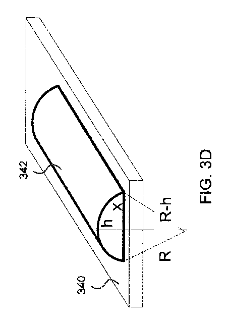
ここで図3A〜Dを参照すると、ドープされたガラスの組(従来のドーピングペーストにおいて用いられている)のシリコン基板上のリフローを、本発明によるシリコンインクを含む高忠実度ドーピングペーストと比較した、簡略図の組が示されている。一般に、シリコンインクは、非ニュートンシリコンナノ粒子コロイド分散体である。より詳細な情報は、2009年6月29日出願の、Sub−Critical Shear Thinning Group IV Based Nanoparticle Fluid、と題する米国特許出願第12/493,946号明細書に記載され、参照によりその特許出願の開示全体を本明細書に組み込む。 Referring now to FIGS. 3A-D, the reflow on a silicon substrate of a doped glass pair (used in conventional doping pastes) was compared to a high fidelity doping paste containing silicon ink according to the present invention. A set of simplified diagrams is shown. In general, silicon ink is a non-Newtonian silicon nanoparticle colloidal dispersion. More detailed information can be found in US patent application Ser. No. 12 / 493,946, filed Jun. 29, 2009, entitled Sub-Critical Shear Thinning Group IV Based Nanoparticulate Fluid. The entire disclosure is incorporated herein.
図3Aは、ドープされたガラスの組に対して、リフロー角度φをリフロー温度℃に対して比較する。リフロー温度は、単位℃で、水平軸302に沿って示し、リフロー角度φは垂直軸に沿って示す。堆積に際して、リフロー角度φは、流体の、空気−ガラス境界とガラス−基板境界との間で形成される。定義によって、流体が広がるにつれて、対応するリフロー角度φは減少する。 FIG. 3A compares the reflow angle φ against the reflow temperature ° C. for a set of doped glasses. The reflow temperature is shown in units of degrees Celsius along the horizontal axis 302 and the reflow angle φ is shown along the vertical axis. Upon deposition, a reflow angle φ is formed between the fluid air-glass boundary and the glass-substrate boundary. By definition, as the fluid spreads, the corresponding reflow angle φ decreases.
ドープされたシリコンガラスは堆積され、次いで、約810℃から約890℃に加熱される。第1のシリコンガラス308は、5%のリンおよび3%のホウ素で構成される。第2のシリコンガラス310は、5%のリンおよび4%のホウ素で構成される。第3のシリコンガラス312は、5%のリンおよび5%のホウ素で構成される。図から分かるように、810℃〜約890℃の流動範囲内の任意の所与の温度に対して、より高いドーパント濃度は、より小さなリフロー角度φに対応する。すなわち、基板表面上のより高い濡れ、およびパターン忠実度の劣化に。
Doped silicon glass is deposited and then heated to about 810 ° C. to about 890 ° C. The
図3Bは、ドープされたガラスの同一の組の正規化された線幅を、本発明によるドープされたシリコンインクと比較する。リフロー角度からの、正規化された線幅の導出は、下記に、図3Cで説明される。 FIG. 3B compares the same set of normalized line widths of doped glass with a doped silicon ink according to the present invention. The derivation of the normalized line width from the reflow angle is described below in FIG. 3C.
第1のシリコンガラス328は、5%のリンおよび3%のホウ素で構成される。第2のシリコンガラス330は、5%のリンおよび4%のホウ素で構成される。第3のシリコンガラス332は、5%のリンおよび5%のホウ素で構成される。さらに、シリコンインク326は、10%のリンのドーパント濃度で構成される。
The
図3Aに見られるように、ガラスの組に対して810℃〜約890℃の流動範囲内の任意の所与の温度にわたって、より高いドーパント濃度は、正規化された線幅においてより大きい差異に対応する。しかしながら、1つの有利な手法では、シリコンインク326は、同一の温度領域にわたって正規化された線幅において本質的な変化を示さない。
As seen in FIG. 3A, over any given temperature within the flow range of 810 ° C. to about 890 ° C. for the glass set, the higher dopant concentration results in a greater difference in normalized line width. Correspond. However, in one advantageous approach, the
図3C〜Dは、リフロー角度から正規化された線幅への変換を導出する。 J.E. Tongらの、Solid State Tech., Jan 1984, p161、を参照されたい。一般に、堆積されたペーストまたはシリコンインクなどの、堆積された流体の小滴344は、円筒の側面の一切れ342としてモデル化されてもよい。以下の導出は、図3A内のリフロー角度φの、図3B内の公称の線幅314への変換を示す。
3C-D derive the transformation from reflow angle to normalized line width. J. et al. E. Tong et al., Solid State Tech. , Jan 1984, p161. In general, a deposited
堆積された流体の形状を円筒の一切れとしてモデル化し、半径Rが計算され得る。 The shape of the deposited fluid can be modeled as a piece of cylinder and the radius R can be calculated.
レオロジー(流動性)比較
実験1
ここで図4A〜Bを参照すると、簡略図の組は、従来のドーピングペーストを、本発明による高忠実度ドーピングペーストと比較する。
Rheology (fluidity)
4A-B, a set of simplified diagrams compares a conventional doping paste with a high fidelity doping paste according to the present invention.
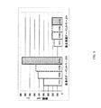
図4Aは、n型Ferroドーピングペースト406(ガラス)、および本発明によるn型シリコンインクベースの高忠実度ドーピングペースト408(非ガラス)の両方に対して粘度対ずり速度を示す。単位1/秒でずり速度の対数402を水平軸に沿って示し、一方、25℃において単位cPで測定された粘度の対数404を、垂直軸に沿って示す。シリコンナノ粒子のペーストの流動挙動への影響を示すために、粘度をずり速度の関数として測定した。図から分かるように、従来のドーピングペースト406は、ゾル粒子の低い表面相互作用のために典型的な近ニュートン挙動を示す。したがって、流体の粘度は、異なるずり速度の下でわずかに変化する。しかしながら、シリコンインクベースの高忠実度ドーピングペースト408は、著しい粒子−粒子相互作用で特徴づけられ、はるかに強いずり減粘挙動を示す。増加したずり減粘挙動は、スクリーンを通るよりよいインク流動の結果をもたらし、図4Bで見られるように、対象面上で、印刷された形状の広がりが低減される。
FIG. 4A shows the viscosity versus shear rate for both n-type Ferro doping paste 406 (glass) and n-type silicon ink based high fidelity doping paste 408 (non-glass) according to the present invention. The logarithm of
図4Bは、同一のスクリーンを用いた堆積の後の、従来のFerro n型ペースト、およびシリコンインクベースの高忠実度ドーピングペーストに対して線幅403を示す。2つのp型基板を、ペースト堆積前にフッ化水素酸と塩酸との混合物を用いて各々洗浄した。両方のペーストを175μmのスクリーンマスク開口部を用いて堆積し、次いで、溶媒を除去し、かつ堆積されたペーストの密度を高めるために200℃で約3分間ベークした。図から分かるように、より強いずり減粘挙動により、高忠実度ドーピングペーストは、従来のドーピングペーストより小さな絶対線幅で堆積することができる。メジアン線幅は、従来のドーピングペーストでは約365μmであり、対して、高忠実度ドーピングペーストでは224μmのメジアン線幅である。175μmのフィンガー開口部に対して、従来のドーピングペーストの190μm拡大と比較して、高忠実度ペーストは約50μmの拡大である。
FIG. 4B shows the
実験2
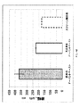
図5は、従来の(Ferro n型)ドーピングペースト(Matthew Edwards,y, Jonathan Bocking, Jeffrey E. Cotter および Neil Bennett; Prog. Photovolt: Res. Appl. 16 (1) pp 31−45, 2008、を参照されたい)と、本発明によるISOのテクスチャー付き基板上でのn型高忠実度ドーピングペーストとの間で、異なる処理段階における平均線幅を比較する。
5 shows a conventional (Ferron type) doping paste (Matthew Edwards, y, Jonathan Bucking, Jeffrey E. Cotter and Neil Bennett; Prog. Photovolt: Res. Appl. 16 (31) p. See) and the n-type high fidelity doping paste on an ISO textured substrate according to the present invention, the average line widths at different processing stages are compared.
従来のドーパントペーストを、400μm(504a)のスクリーン開口部を通して印刷し、約520μm(506a)の印刷された線幅を結果として得て、次いで、溶媒を除去し、かつ堆積されたペーストの密度を高めるために300℃で1〜2分間ベークし、約570μm(508a)の線幅を結果として得たが、スクリーンマスク開口部より約40%の増加した。ドーパントを基板へ拡散するため、従来のドーパントペーストを、950℃の温度に90分間加熱し、約870μm(510a)の、または元のスクリーン開口部の217.5%のドーパント幅を結果として得た。 A conventional dopant paste is printed through a 400 μm (504a) screen opening, resulting in a printed line width of about 520 μm (506a), then the solvent is removed and the density of the deposited paste is reduced. Baking at 300 ° C. for 1-2 minutes to increase, resulting in a line width of about 570 μm (508a), but increased by about 40% over the screen mask opening. In order to diffuse the dopant into the substrate, a conventional dopant paste was heated to a temperature of 950 ° C. for 90 minutes, resulting in a dopant width of about 870 μm (510a) or 217.5% of the original screen opening. .
高忠実度ドーピングペーストに対して、175μm(504b)のスクリーンマスク開口部をペーストを堆積するために用いて、約220μm(506b)の堆積された幅を結果として得たが、約20%の増加となった。次いで、溶媒を除去し、かつ堆積されたペーストの密度を高めるために,従来のドーパントペーストを200℃で約3分間ベークした。しかしながら、結果として得られた線幅は、スクリーン開口部(508b)より約20%の拡大にとどまった。次いで、基板へドーパントを拡散するために、高忠実度ドーパントペーストを950℃の温度に90分間加熱した。前述同様に、また従来のドーピングペーストと異なり、結果として得られた線幅はスクリーン形状開口部(510b)の約120%にとどまった。 For high fidelity doping pastes, a 175 μm (504b) screen mask opening was used to deposit the paste, resulting in a deposited width of about 220 μm (506b), but an increase of about 20% It became. The conventional dopant paste was then baked at 200 ° C. for about 3 minutes in order to remove the solvent and increase the density of the deposited paste. However, the resulting line width was only about 20% larger than the screen opening (508b). The high fidelity dopant paste was then heated to a temperature of 950 ° C. for 90 minutes in order to diffuse the dopant into the substrate. As before, and unlike conventional doping pastes, the resulting line width was only about 120% of the screen-shaped opening (510b).
ドーピング比較
図6は、本発明による、高忠実度ドーピングペーストとともに使用する背中合わせのドーパント拡散構成の簡略図を示す。
Doping Comparison FIG. 6 shows a simplified diagram of a back-to-back dopant diffusion configuration for use with a high fidelity doping paste according to the present invention.
ドーピング環境中にドーピングペーストから揮発性になる環境ドーパントの影響を最小限に抑えるために、シリコン基板604を背中合わせの構成で垂直に置く。N2環境において、堆積されたFerroドーピングペースト、および高忠実度ドーピングペースト606を、(それぞれに見合って)対応する基板で覆うために、p型シリコン基板604を背中合わせで、横型拡散炉内の石英チューブ内に垂直に置いた。
In order to minimize the effects of environmental dopants that become volatile from the doping paste during the doping environment, the
実験3
ここで図7を参照すると、本発明による、(2ohm−cm/180μm/切断損傷エッチング済み)p型シリコン基板の組の上のHFドーピングペーストのシート抵抗を、Ferro n型ドーピングペーストと比較する簡略図。発明者らは、Ferroドーピングペーストのドーピングプロファイルは、ほとんどのドーピングペーストに相当に類似していると考える。
Referring now to FIG. 7, a simplified comparison of the sheet resistance of HF doping paste over a set of p-type silicon substrates (2 ohm-cm / 180 μm / cut damage etched) according to the present invention compared to Ferron type doping paste. Figure. The inventors believe that the doping profile of the Ferro doping paste is quite similar to most doping pastes.
テルピネオール溶媒中に1.5重量%のエチルセルロースバインダー、および8重量%のシリコンナノ粒子を含有するSiナノ粒子ペーストに、10%のリン酸を付加することによって、高忠実度ドーピングペーストを調製し、続けて、遊星型ミキサーで完全に混合した。従来の(Ferro)ドーピングペーストは未変更で用いた。p型シリコン基板の組を、ペースト堆積前にフッ化水素酸と塩酸との混合物でおのおの洗浄した。 A high fidelity doping paste was prepared by adding 10% phosphoric acid to a Si nanoparticle paste containing 1.5 wt% ethylcellulose binder and 8 wt% silicon nanoparticles in terpineol solvent; Subsequently, it was thoroughly mixed with a planetary mixer. The conventional (Ferro) doping paste was used unchanged. Each set of p-type silicon substrates was each cleaned with a mixture of hydrofluoric acid and hydrochloric acid prior to paste deposition.
Ferroペーストおよび高忠実度ドーピングペーストを3つの独立した基板下位組の上におのおの堆積した。次いで、高忠実度ドーピングペーストを有する基板下位組を、薄膜の密度を高めるため、かつリン酸を脱水するために、N2環境において200℃で3分間ベークした。次いで、リンのドーパントをドライブインするためにすべての基板下位組を、N2環境を備えた石英チューブ内で30分間加熱した。第1の下位組は860℃に加熱し、第2の下位組は900℃に加熱し、第3の下位組は1000℃に加熱した。次いで、すべての基板下位組を、10分間のBOEで洗浄し、インク領域の下のシート抵抗を、4探針を用いて測定した。一般に、4探針は、外側の2つの探針を通る高インピーダンスの電流源を供給すること、および内側の2つの探針の両端の電圧を測定することによってサンプルの抵抗率を測定する。 Ferro paste and high fidelity doping paste were each deposited on three independent substrate subsets. The substrate sub-set with the high fidelity doping paste was then baked at 200 ° C. for 3 minutes in an N 2 environment to increase the density of the thin film and to dehydrate the phosphoric acid. All substrate sub-sets were then heated in a quartz tube with N 2 environment for 30 minutes to drive in the phosphorus dopant. The first sub-set was heated to 860 ° C., the second sub-set was heated to 900 ° C., and the third sub-set was heated to 1000 ° C. All substrate sub-sets were then washed with 10 minutes of BOE and the sheet resistance under the ink area was measured using a 4-probe. In general, a four probe measures the resistivity of a sample by providing a high impedance current source through the two outer probes and measuring the voltage across the two inner probes.
860℃のドライブイン温度で、Ferroペーストを有する基板のシート抵抗は、約330ohm/sqであり、一方、HFドーピングペーストを有する基板のシート抵抗は、約237ohm/sqである。900℃のドライブイン温度で、Ferroペーストを有する基板のシート抵抗は、約372ohm/sqであり、一方、HFドーピングペーストを有する基板のシート抵抗は、約161ohm/sqである。また1000℃のドライブイン温度で、Ferroペーストを有する基板のシート抵抗は、約224ohm/sqであり、一方、HFドーピングペーストを有する基板のシート抵抗は、約75ohm/sqである。図から分かるように、任意の所与の温度に対して、より低いシート抵抗、したがって、より高いドーパント濃度が基板にドライブインされている。 At a drive-in temperature of 860 ° C., the sheet resistance of the substrate with Ferro paste is about 330 ohm / sq, whereas the sheet resistance of the substrate with HF doping paste is about 237 ohm / sq. At a drive-in temperature of 900 ° C., the sheet resistance of the substrate with Ferro paste is about 372 ohm / sq, while the sheet resistance of the substrate with HF doping paste is about 161 ohm / sq. Also, at a drive-in temperature of 1000 ° C., the sheet resistance of the substrate with Ferro paste is about 224 ohm / sq, while the sheet resistance of the substrate with HF doping paste is about 75 ohm / sq. As can be seen, for any given temperature, a lower sheet resistance and thus a higher dopant concentration is driven into the substrate.
実験4
ここで図8を参照すると、本発明による、(2ohm−cm/180μm/切断損傷エッチング済み)p型シリコン基板の組の上の、様々なn型高忠実度ドーピングペースト構成のシート抵抗を比較する簡略図。
Referring now to FIG. 8, compare the sheet resistance of various n-type high fidelity doping paste configurations on a (2 ohm-cm / 180 μm / cut damage etched) p-type silicon substrate set according to the present invention. Simplified schematic.
シート抵抗(ohm/sq)802を垂直軸に沿って示し、一方、露出804、ドーピング濃度%806、およびドライブイン温度(℃)808を、水平軸に沿って示す。
Sheet resistance (ohm / sq) 802 is shown along the vertical axis, while
前述したように、テルピネオール溶媒中に1.5重量%のエチルセルロースバインダー、および8重量%のシリコンナノ粒子を含有するSiナノ粒子ペーストに、5%、10%、または18%のリン酸を付加することによって、高忠実度ドーピングペーストを調製し、続けて、遊星型ミキサーで完全に混合した。従来の(Ferro)ドーピングペーストは未変更で用いた。 As described above, 5%, 10%, or 18% phosphoric acid is added to Si nanoparticle paste containing 1.5 wt% ethylcellulose binder and 8 wt% silicon nanoparticles in terpineol solvent. A high fidelity doping paste was prepared, followed by thorough mixing with a planetary mixer. The conventional (Ferro) doping paste was used unchanged.
p型シリコン基板の組を、ペースト堆積前にフッ化水素酸と塩酸との混合物でおのおの洗浄した。次いで、基板下位組を、溶媒を除去するために、200℃で3分間ベークした。次いで、すべての基板下位組を、リン酸を脱水するために、かつリンのドーパントをドライブインするために、N2環境を備えた石英チューブ内で加熱した。覆われたウエハーは、加熱された石英チューブ内に、図6に説明した背中合わせの構成を用いて置いた。さらされたウエハーは、加熱された石英チューブ内に、インク領域がN2環境に直接さらされたまま置いた。 Each set of p-type silicon substrates was each cleaned with a mixture of hydrofluoric acid and hydrochloric acid prior to paste deposition. The substrate sub-set was then baked at 200 ° C. for 3 minutes to remove the solvent. All substrate subsets were then heated in a quartz tube with an N 2 environment to dehydrate the phosphoric acid and drive in the phosphorus dopant. The covered wafer was placed in a heated quartz tube using the back-to-back configuration described in FIG. The exposed wafer was placed in a heated quartz tube with the ink area directly exposed to the N 2 environment.
860℃のドライブイン温度、および5%のリンのドーピング濃度で、さらされた基板のシート抵抗は、約267ohm/sqであり、一方、覆われた基板のシート抵抗は、約162ohm/sqである。 At a drive-in temperature of 860 ° C. and a doping concentration of 5% phosphorus, the sheet resistance of the exposed substrate is about 267 ohm / sq, while the sheet resistance of the covered substrate is about 162 ohm / sq. .
860℃のドライブイン温度で、および10%のリンのドーピング濃度で、さらされた基板のシート抵抗は、約237ohm/sqであり、一方、覆われた基板のシート抵抗は、約127ohm/sqである。 At a drive-in temperature of 860 ° C. and at a doping concentration of 10% phosphorus, the sheet resistance of the exposed substrate is about 237 ohm / sq, while the sheet resistance of the covered substrate is about 127 ohm / sq. is there.
860℃のドライブイン温度で、および18%のリンのドーピング濃度で、さらされた基板のシート抵抗は、約126ohm/sqであり、一方、覆われた基板のシート抵抗は、約83ohm/sqである。 At a drive-in temperature of 860 ° C. and a phosphorus doping concentration of 18%, the sheet resistance of the exposed substrate is about 126 ohm / sq, while the sheet resistance of the covered substrate is about 83 ohm / sq. is there.
900℃のドライブイン温度で、および5%のリンのドーピング濃度で、さらされた基板のシート抵抗は、約198ohm/sqであり、一方、覆われた基板のシート抵抗は、約112ohm/sqである。 At a drive-in temperature of 900 ° C. and at a doping concentration of 5% phosphorus, the sheet resistance of the exposed substrate is about 198 ohm / sq, while the sheet resistance of the covered substrate is about 112 ohm / sq. is there.
900℃のドライブイン温度で、および10%のリンのドーピング濃度で、さらされた基板のシート抵抗は、約160ohm/sqであり、基板の覆われたシート抵抗が約89オーム/sqである。 At a drive-in temperature of 900 ° C. and at a doping concentration of 10% phosphorus, the sheet resistance of the exposed substrate is about 160 ohm / sq and the covered sheet resistance of the substrate is about 89 ohm / sq.
900℃のドライブイン温度で、および18%のリンのドーピング濃度で、さらされた基板のシート抵抗は、約89ohm/sqであり、一方、覆われた基板のシート抵抗は、約57ohm/sqである。 At a drive-in temperature of 900 ° C. and at a 18% phosphorus doping concentration, the sheet resistance of the exposed substrate is about 89 ohm / sq, while the sheet resistance of the covered substrate is about 57 ohm / sq. is there.
1000℃のドライブイン温度で、および5%のリンのドーピング濃度で、さらされた基板のシート抵抗は、約114ohm/sqであり、一方、覆われた基板のシート抵抗は、約42ohm/sqである。 At a drive-in temperature of 1000 ° C. and at a 5% phosphorus doping concentration, the sheet resistance of the exposed substrate is about 114 ohm / sq, while the sheet resistance of the covered substrate is about 42 ohm / sq. is there.
1000℃のドライブイン温度で、および10%のリンのドーピング濃度で、さらされた基板のシート抵抗は、約75ohm/sqであり、一方、覆われた基板のシート抵抗は、約52ohm/sqである。 At a drive-in temperature of 1000 ° C. and at a doping concentration of 10% phosphorus, the sheet resistance of the exposed substrate is about 75 ohm / sq, while the sheet resistance of the covered substrate is about 52 ohm / sq. is there.
1000℃のドライブイン温度で、および18%のリンのドーピング濃度で、さらされた基板のシート抵抗は、約36ohm/sqであり、一方、覆われた基板のシート抵抗は、約41ohm/sqである。 At a drive-in temperature of 1000 ° C. and at a 18% phosphorus doping concentration, the sheet resistance of the exposed substrate is about 36 ohm / sq, while the sheet resistance of the covered substrate is about 41 ohm / sq. is there.
図から分かるように、任意の所与の温度に対して、より低いシート抵抗、したがって、より高いドーパント濃度が基板にドライブインされている。 As can be seen, for any given temperature, a lower sheet resistance and thus a higher dopant concentration is driven into the substrate.
実験5
ここで図9A〜Bを参照すると、本発明による、(2ohm−cm/180μm/切断損傷エッチング済み)n型シリコン基板の組の上の、様々なp型(ホウ素)高忠実度ドーピングペースト構成のシート抵抗を比較する簡略図の組。図9Aは対数目盛上にデータを表示し、一方、図9Bは均等目盛上にデータを表示する。
Referring now to FIGS. 9A-B, various p-type (boron) high fidelity doping paste configurations on an n-type silicon substrate set (2 ohm-cm / 180 μm / cut damage etched) according to the present invention. A set of simplified diagrams comparing sheet resistance. FIG. 9A displays data on a logarithmic scale, while FIG. 9B displays data on a uniform scale.
シート抵抗(ohm/sq)902を垂直軸に沿って示し、一方、露出904、ドーピング濃度%906、およびドライブイン温度(℃)908を、水平軸に沿って示す。
Sheet resistance (ohm / sq) 902 is shown along the vertical axis, while
前述したように、テルピネオール溶媒中に1.5重量%のエチルセルロースバインダー、および8重量%のシリコンナノ粒子を含有するSiナノ粒子ペーストに、5%、10%、または19%のホウ酸トリエチルを付加することによって、高忠実度ドーピングペーストを調製し、続けて、遊星型ミキサーで完全に混合した。 Add 5%, 10%, or 19% triethyl borate to Si nanoparticle paste containing 1.5 wt% ethylcellulose binder and 8 wt% silicon nanoparticles in terpineol solvent as described above. A high fidelity doping paste was prepared, followed by thorough mixing with a planetary mixer.
3つの高忠実度ドーピングペーストホウ素濃度を調製した(5%、10%および19%)。n型シリコン基板の組を、ペースト堆積前にフッ化水素酸と塩酸との混合物によりおのおの洗浄した。次いで、薄膜の密度を高めるため、基板下位組を、N2環境において200℃で3分間ベークした。次いで、すべての基板下位組を、ホウ素のドーパントをドライブインするために、N2環境を備えた石英チューブ内で30分間加熱した。 Three high fidelity doping paste boron concentrations were prepared (5%, 10% and 19%). Each set of n-type silicon substrates was each washed with a mixture of hydrofluoric acid and hydrochloric acid prior to paste deposition. The substrate sub-set was then baked at 200 ° C. for 3 minutes in an N 2 environment to increase the density of the thin film. All substrate sub-sets were then heated in a quartz tube with an N 2 environment for 30 minutes to drive in the boron dopant.
860℃のドライブイン温度で、および5%のホウ素ドーピング濃度で、さらされた基板のシート抵抗は、約1588ohm/sqであり、一方、覆われた基板のシート抵抗は、約431ohm/sqである。 At a drive-in temperature of 860 ° C. and at a boron doping concentration of 5%, the sheet resistance of the exposed substrate is about 1588 ohm / sq, while the sheet resistance of the covered substrate is about 431 ohm / sq. .
860℃のドライブイン温度で、および10%のホウ素ドーピング濃度で、さらされた基板のシート抵抗は、約889ohm/sqであり、一方、覆われた基板のシート抵抗は、約268ohm/sqである。 At a drive-in temperature of 860 ° C. and at a boron doping concentration of 10%, the sheet resistance of the exposed substrate is about 889 ohm / sq, while the sheet resistance of the covered substrate is about 268 ohm / sq. .
860℃のドライブイン温度で、および19%のホウ素ドーピング濃度で、さらされた基板のシート抵抗は、約629ohm/sqであり、一方、覆われた基板のシート抵抗は、約247ohm/sqである。 At a drive-in temperature of 860 ° C. and at a boron doping concentration of 19%, the sheet resistance of the exposed substrate is about 629 ohm / sq, while the sheet resistance of the covered substrate is about 247 ohm / sq. .
900℃のドライブイン温度で、および5%のホウ素ドーピング濃度で、さらされた基板のシート抵抗は、約1232ohm/sqであり、一方、覆われた基板のシート抵抗は、約231ohm/sqである。 At a drive-in temperature of 900 ° C. and at a boron doping concentration of 5%, the sheet resistance of the exposed substrate is about 1232 ohm / sq, while the sheet resistance of the covered substrate is about 231 ohm / sq. .
900℃のドライブイン温度で、および10%のホウ素ドーピング濃度で、さらされた基板のシート抵抗は、約603ohm/sqであり、一方、覆われた基板のシート抵抗は、約171ohm/sqである。 At a drive-in temperature of 900 ° C. and at a boron doping concentration of 10%, the sheet resistance of the exposed substrate is about 603 ohm / sq, while the sheet resistance of the covered substrate is about 171 ohm / sq. .
900℃のドライブイン温度で、および19%のホウ素ドーピング濃度で、さらされた基板のシート抵抗は、約520ohm/sqであり、一方、覆われた基板のシート抵抗は、約154ohm/sqである。 At a drive-in temperature of 900 ° C. and at a boron doping concentration of 19%, the sheet resistance of the exposed substrate is about 520 ohm / sq, while the sheet resistance of the covered substrate is about 154 ohm / sq. .
1000℃のドライブイン温度で、および5%のホウ素ドーピング濃度で、さらされた基板のシート抵抗は、約653ohm/sqであり、一方、覆われた基板のシート抵抗は、約58ohm/sqである。 At a drive-in temperature of 1000 ° C. and at a boron doping concentration of 5%, the sheet resistance of the exposed substrate is about 653 ohm / sq, while the sheet resistance of the covered substrate is about 58 ohm / sq. .
1000℃のドライブイン温度で、および10%のホウ素ドーピング濃度で、さらされた基板のシート抵抗は、約297ohm/sqであり、一方、覆われた基板のシート抵抗は、約43ohm/sqである。 At a drive-in temperature of 1000 ° C. and at a boron doping concentration of 10%, the sheet resistance of the exposed substrate is about 297 ohm / sq, while the sheet resistance of the covered substrate is about 43 ohm / sq. .
1000℃のドライブイン温度で、および19%のホウ素ドーピング濃度で、さらされた基板のシート抵抗は、約105ohm/sqであり、一方、覆われた基板のシート抵抗は、約43ohm/sqである。 At a drive-in temperature of 1000 ° C. and at a boron doping concentration of 19%, the sheet resistance of the exposed substrate is about 105 ohm / sq, while the sheet resistance of the covered substrate is about 43 ohm / sq. .
図から分かるように、任意の所与の温度に対して、より低いシート抵抗、したがって、より高いドーパント濃度が基板にドライブインされている。 As can be seen, for any given temperature, a lower sheet resistance and thus a higher dopant concentration is driven into the substrate.
説明的に本明細書で記述された本発明は、いかなる素子または素子群、限定または限定群が欠けていても、特に本明細書で開示されていなくても、適切に実行されてもよい。したがって、たとえば、用語「備える」、「含む」、「包含している」などは、拡張的に、かつ、限定せずに読まれるものとする。さらに、本明細書で使用された用語と表現は、記述の用語として使用されたもので、限定の用語として使用されたものではなく、そのような用語および表現の使用において、示され、記述された特徴およびその特徴の部分の、いかなる均等物も除外する意図はなく、様々な変更が請求された本発明の請求の範囲内で可能であることが認識されるはずである。 The invention described herein in an illustrative manner may be suitably practiced without any elements or groups of elements, limitations or groups of limitations, and not specifically disclosed herein. Thus, for example, the terms “comprising”, “including”, “including”, etc. shall be read in an expanded and non-limiting manner. Further, the terms and expressions used herein are used as descriptive terms, not as limiting terms, and are shown and described in the use of such terms and expressions. It should be recognized that the present invention is not intended to exclude any equivalents of features and portions thereof, and that various modifications are possible within the scope of the claimed invention.
したがって、本発明を、好ましい実施形態および任意選択的な特徴によって具体的に開示してきたが、本明細書で開示された本発明の修正、改善および変更が当業者によって行使されてもよいこと、および、そのような修正、改善および変更は、本発明の範囲内であると見なされることは、理解すべきである。本明細書で提供される材料、方法、および実施例は、好ましい実施形態の代表的なものであり、例示になるものであり、本発明の範囲に対する限定として意図されたものではない。 Thus, while the present invention has been specifically disclosed by preferred embodiments and optional features, modifications, improvements and changes of the invention disclosed herein may be exercised by those skilled in the art. It should also be understood that such modifications, improvements, and changes are considered within the scope of the present invention. The materials, methods, and examples provided herein are representative of preferred embodiments, are exemplary, and are not intended as limitations on the scope of the invention.
当業者によって理解される通り、いかなる、かつ、全ての目的に対しても、特に書面による記述の提供の点で、本明細書で開示された全ての範囲はまた、その範囲の、いかなる、かつ、全ての可能な下位の範囲およびそれらの下位の範囲の組み合わせを包含する。いかなる列挙された範囲も、その同じ範囲が少なくとも、等分、3等分、4等分、5等分、10等分などに分割されることを、十分に記述し可能にしているものとして、容易に認めることができる。非限定例として、本明細書で説明された範囲はおのおの、下側の3分の1、中央の3分の1、上側の3分の1へ容易に分割できる。さらに当業者によって理解されるように、「まで」、「少なくとも」、「より大きい」、「より小さい」および同種のものなど、全ての言葉は詳述された数を含み、かつ、上記に説明したとおり、下位の範囲に後で分割することができる範囲を表す。さらに、用語「ドーパント、またはドープされた」および「カウンタードーパント、またはカウンタードープされた」は反対の型のドーパントの組を表す。すなわち、ドーパントがp型である場合、カウンタードーパントはn型である。さらに、特に断らない限り、ドーパントの型は入れ替えてもよい。さらに、シリコン基板は、単結晶状、または多結晶状でもよい。さらに、「無ドープの」は、ドーパントが欠如している材料を指す。本明細書に記載の通り、ケトン分子およびアルコール分子は、環式、直線、または、分岐であってもよい。 As will be appreciated by those skilled in the art, all ranges disclosed herein for any and all purposes, particularly in terms of providing a written description, are also within the scope of any and all , Including all possible subranges and combinations of those subranges. Any enumerated range shall be sufficiently described and made possible that the same range is divided into at least equal, 3 equal, 4 equal, 5 equal, 10 equal, etc. It can be easily recognized. As a non-limiting example, each of the ranges described herein can be easily divided into a lower third, a middle third, and an upper third. Further, as will be understood by those skilled in the art, all terms including “up to”, “at least”, “greater than”, “less than” and the like include the detailed numbers and are described above. As indicated, it represents a range that can be later divided into lower ranges. Furthermore, the terms “dopant or doped” and “counter dopant or counterdoped” represent a set of opposite types of dopants. That is, when the dopant is p-type, the counter-dopant is n-type. Furthermore, unless otherwise specified, the dopant type may be changed. Further, the silicon substrate may be single crystal or polycrystalline. Furthermore, “undoped” refers to a material that lacks a dopant. As described herein, ketone and alcohol molecules may be cyclic, linear, or branched.
さらに、本発明は、2008年2月12日出願の、Methods and Apparatus for Creating Junctions on a Substrate、と題する米国特許出願第12/029,838号明細書に記載されるような他の太陽電池構造に適用されてもよく、参照によりその特許出願の開示全体を本明細書に組み込む。 Furthermore, the present invention relates to other solar cell structures as described in US patent application Ser. No. 12 / 029,838, filed Feb. 12, 2008, entitled Methods and Apparatus for Creating Junctions on a Substrate. And the entire disclosure of that patent application is incorporated herein by reference.
本明細書で参照された全ての刊行物、特許出願、登録特許、および他の文献は、おのおのの個別の、刊行物、特許出願、登録特許、および他の文献を具体的かつ個別に引用した場合その全体を組み込むのと同程度に、参照により、本明細書に組み込む。参照によって組み込まれたテキストに包含されている定義は、本開示中の定義と矛盾する範囲については除外される。 All publications, patent applications, registered patents, and other references referred to herein are specifically and individually referenced to each individual publication, patent application, registered patent, and other reference. Incorporated herein by reference to the same extent as if fully incorporated. Definitions included in text incorporated by reference are excluded to the extent that they contradict definitions in this disclosure.
本開示の目的のために、および特に指定がない限り、「1つ」は「1つまたは複数」を意味する。本明細書に引用した全ての特許、特許出願、参考文献、および刊行物は、それらが個別に参照として組み込まれている場合と同程度に、それらの全体を参照として組み込む。さらに、単語「組」は、1つまたは複数の、品目または物の、集合を指す。 For the purposes of this disclosure and unless otherwise specified, “one” means “one or more”. All patents, patent applications, references, and publications cited herein are incorporated by reference in their entirety as if they were individually incorporated by reference. Further, the word “set” refers to a collection of one or more items or things.
本発明の利点は、太陽電池の大量生産におけるスクリーン印刷に対して最適化された高忠実度ドーピングペーストを含む。 The advantages of the present invention include a high fidelity doping paste optimized for screen printing in mass production of solar cells.
例示的な実施形態および最良の形態を開示してきたが、以下の特許請求の範囲によって定義される本発明の主題および精神の範囲内で、開示した実施形態に修正および変更を施すことができる。 While exemplary embodiments and best modes have been disclosed, modifications and changes may be made to the disclosed embodiments within the scope and spirit of the invention as defined by the following claims.
Claims (19)
前記溶媒へ分散された非ガラスマトリックス粒子の組と、
ドーパントと、
を含む高忠実度ドーパントペースト。 A solvent,
A set of non-glass matrix particles dispersed in the solvent;
A dopant,
High fidelity dopant paste containing.
Applications Claiming Priority (3)
| Application Number | Priority Date | Filing Date | Title |
|---|---|---|---|
| US12/967,654 US8858843B2 (en) | 2010-12-14 | 2010-12-14 | High fidelity doping paste and methods thereof |
| US12/967,654 | 2010-12-14 | ||
| PCT/US2011/064954 WO2012082926A2 (en) | 2010-12-14 | 2011-12-14 | High fidelity doping paste and methods thereof |
Publications (2)
| Publication Number | Publication Date |
|---|---|
| JP2014505357A true JP2014505357A (en) | 2014-02-27 |
| JP2014505357A5 JP2014505357A5 (en) | 2015-02-12 |
Family
ID=45491769
Family Applications (1)
| Application Number | Title | Priority Date | Filing Date |
|---|---|---|---|
| JP2013544748A Pending JP2014505357A (en) | 2010-12-14 | 2011-12-14 | High fidelity doping paste and method thereof |
Country Status (5)
| Country | Link |
|---|---|
| US (2) | US8858843B2 (en) |
| JP (1) | JP2014505357A (en) |
| CN (1) | CN103403878B (en) |
| TW (1) | TW201237944A (en) |
| WO (1) | WO2012082926A2 (en) |
Cited By (2)
| Publication number | Priority date | Publication date | Assignee | Title |
|---|---|---|---|---|
| JP2015005621A (en) * | 2013-06-20 | 2015-01-08 | 株式会社ノリタケカンパニーリミテド | Solar battery substrate and method of manufacturing the same |
| JPWO2021045186A1 (en) * | 2019-09-05 | 2021-09-27 | 日立金属株式会社 | Manufacturing method of thermoelectric conversion module |
Families Citing this family (15)
| Publication number | Priority date | Publication date | Assignee | Title |
|---|---|---|---|---|
| US9196486B2 (en) | 2012-10-26 | 2015-11-24 | Innovalight, Inc. | Inorganic phosphate containing doping compositions |
| US20140166093A1 (en) * | 2012-12-18 | 2014-06-19 | Paul Loscutoff | Solar cell emitter region fabrication using n-type doped silicon nano-particles |
| CN103280401B (en) * | 2013-05-23 | 2016-01-27 | 刘国钧 | A kind of preparation method of boron composition coated Si nano pulp and application thereof |
| CN103280491B (en) * | 2013-05-23 | 2015-11-04 | 苏州金瑞晨科技有限公司 | A kind of preparation method of polyborate nanometer silicon composite slurry and application thereof |
| CN103489932B (en) * | 2013-09-04 | 2016-03-30 | 苏州金瑞晨科技有限公司 | A kind of nano-silicon phosphorus slurry and its preparation method and application |
| CN103606395B (en) * | 2013-11-08 | 2016-02-10 | 四川大学 | Containing the silicon slurry of multiple hydrogen bonding Supramolecular self assembly system and the application in solar cell |
| US9048374B1 (en) | 2013-11-20 | 2015-06-02 | E I Du Pont De Nemours And Company | Method for manufacturing an interdigitated back contact solar cell |
| CN103714879B (en) * | 2013-12-27 | 2016-08-17 | 苏州金瑞晨科技有限公司 | Nano-silicon boron slurry and the technique being applied to prepare full-shield boron back surface field thereof |
| US9059341B1 (en) | 2014-01-23 | 2015-06-16 | E I Du Pont De Nemours And Company | Method for manufacturing an interdigitated back contact solar cell |
| JP6072129B2 (en) | 2014-04-30 | 2017-02-01 | ザ リージェンツ オブ ザ ユニバーシティ オブ カリフォルニア | Doping of substrates using dopant-containing polymer films |
| CN104617164A (en) * | 2015-02-11 | 2015-05-13 | 苏州金瑞晨科技有限公司 | Nano silicon boron slurry and method for preparing solar cell with the same |
| US9306088B1 (en) | 2015-09-17 | 2016-04-05 | E I Du Pont De Nemours And Company | Method for manufacturing back contact solar cells |
| CN107749320A (en) * | 2017-09-25 | 2018-03-02 | 江苏时瑞电子科技有限公司 | A kind of electrocondution slurry of antimony dopant and zirconium and preparation method thereof |
| DE102018109571B4 (en) * | 2018-04-20 | 2021-09-02 | Karlsruher Institut für Technologie | Method for doping semiconductors |
| CN110292919B (en) * | 2019-07-23 | 2020-08-14 | 北京大学 | Boron oxide and titanium dioxide composite nano material and preparation method thereof |
Citations (10)
| Publication number | Priority date | Publication date | Assignee | Title |
|---|---|---|---|---|
| JPS622472B2 (en) * | 1981-07-27 | 1987-01-20 | Handotai Energy Kenkyusho | |
| JPH03119722A (en) * | 1989-10-03 | 1991-05-22 | Tokyo Ohka Kogyo Co Ltd | Dopant film and impurity diffusion using it |
| JP2000021794A (en) * | 1998-07-03 | 2000-01-21 | Nec Yamagata Ltd | Manufacture of semiconductor wafer |
| JP2007521668A (en) * | 2004-02-05 | 2007-08-02 | アドベント ソーラー,インク. | Back contact solar cell and its manufacturing method |
| US20090142911A1 (en) * | 2005-08-12 | 2009-06-04 | Naoki Asano | Masking paste, method of manufacturing same, and method of manufacturing solar cell using masking paste |
| JP2009530845A (en) * | 2006-03-20 | 2009-08-27 | フエロ コーポレーション | Aluminum-boron solar cell contact |
| JP2010056465A (en) * | 2008-08-29 | 2010-03-11 | Shin-Etsu Chemical Co Ltd | Boron paste for diffusion, and method of manufacturing solar cell using the same |
| JP2010062334A (en) * | 2008-09-03 | 2010-03-18 | Japan Vam & Poval Co Ltd | Coating liquid for diffusing phosphor |
| WO2010050936A1 (en) * | 2008-10-29 | 2010-05-06 | Innovalight, Inc. | Methods of forming multi-doped junctions on a substrate |
| JP2010205839A (en) * | 2009-03-02 | 2010-09-16 | Sharp Corp | Method of manufacturing semiconductor device |
Family Cites Families (19)
| Publication number | Priority date | Publication date | Assignee | Title |
|---|---|---|---|---|
| US2983808A (en) | 1957-08-22 | 1961-05-09 | British Oxygen Co Ltd | Electric arc welding |
| US4891331A (en) * | 1988-01-21 | 1990-01-02 | Oi-Neg Tv Products, Inc. | Method for doping silicon wafers using Al2 O3 /P2 O5 composition |
| DE19910816A1 (en) * | 1999-03-11 | 2000-10-05 | Merck Patent Gmbh | Doping pastes for producing p, p + and n, n + regions in semiconductors |
| US20060060238A1 (en) * | 2004-02-05 | 2006-03-23 | Advent Solar, Inc. | Process and fabrication methods for emitter wrap through back contact solar cells |
| US7335555B2 (en) * | 2004-02-05 | 2008-02-26 | Advent Solar, Inc. | Buried-contact solar cells with self-doping contacts |
| US7217781B2 (en) * | 2004-04-20 | 2007-05-15 | Parallel Solutions, Inc. | Polyphosphazenes including ionic or ionizable moieties and fluorine-containing moieties |
| US7825422B2 (en) * | 2004-08-18 | 2010-11-02 | Tokuyama Corporation | Ceramic substrate for mounting a light emitting element and method for manufacturing the same |
| US20060084566A1 (en) * | 2004-10-19 | 2006-04-20 | General Electric Company | Multiphase ceramic nanocomposites and method of making them |
| US7556748B2 (en) * | 2005-04-14 | 2009-07-07 | E. I. Du Pont De Nemours And Company | Method of manufacture of semiconductor device and conductive compositions used therein |
| US7435361B2 (en) * | 2005-04-14 | 2008-10-14 | E.I. Du Pont De Nemours And Company | Conductive compositions and processes for use in the manufacture of semiconductor devices |
| DE102005025933B3 (en) * | 2005-06-06 | 2006-07-13 | Centrotherm Photovoltaics Gmbh + Co. Kg | Doping mixture for preparing and doping semiconductor surfaces, comprises a p- or n-dopant, for doping the semiconductor surfaces, water and mixture of two or more surfactants, where one of the surfactant is a non-ionic surfactant |
| WO2008070632A1 (en) * | 2006-12-01 | 2008-06-12 | Advent Solar, Inc. | Phosphorus-stabilized transition metal oxide diffusion barrier |
| WO2008078374A1 (en) * | 2006-12-25 | 2008-07-03 | Namics Corporation | Conductive paste for solar cell |
| US8309844B2 (en) * | 2007-08-29 | 2012-11-13 | Ferro Corporation | Thick film pastes for fire through applications in solar cells |
| US20100275982A1 (en) | 2007-09-04 | 2010-11-04 | Malcolm Abbott | Group iv nanoparticle junctions and devices therefrom |
| KR101631711B1 (en) * | 2008-03-21 | 2016-06-17 | 신에쓰 가가꾸 고교 가부시끼가이샤 | Phosphorus paste for diffusion and method for preparing solar cell by using the same |
| JP5357442B2 (en) * | 2008-04-09 | 2013-12-04 | 東京応化工業株式会社 | Inkjet diffusing agent composition, electrode using the composition, and method for producing solar cell |
| US9198843B2 (en) * | 2008-08-11 | 2015-12-01 | Jan R Prochazka | Process for manufacturing of high surface area USP grade nano-anatase base |
| US7910393B2 (en) | 2009-06-17 | 2011-03-22 | Innovalight, Inc. | Methods for forming a dual-doped emitter on a silicon substrate with a sub-critical shear thinning nanoparticle fluid |
-
2010
- 2010-12-14 US US12/967,654 patent/US8858843B2/en active Active
-
2011
- 2011-12-13 TW TW100145907A patent/TW201237944A/en unknown
- 2011-12-14 JP JP2013544748A patent/JP2014505357A/en active Pending
- 2011-12-14 CN CN201180058799.4A patent/CN103403878B/en active Active
- 2011-12-14 WO PCT/US2011/064954 patent/WO2012082926A2/en active Application Filing
-
2014
- 2014-08-28 US US14/471,687 patent/US20140370640A1/en not_active Abandoned
Patent Citations (10)
| Publication number | Priority date | Publication date | Assignee | Title |
|---|---|---|---|---|
| JPS622472B2 (en) * | 1981-07-27 | 1987-01-20 | Handotai Energy Kenkyusho | |
| JPH03119722A (en) * | 1989-10-03 | 1991-05-22 | Tokyo Ohka Kogyo Co Ltd | Dopant film and impurity diffusion using it |
| JP2000021794A (en) * | 1998-07-03 | 2000-01-21 | Nec Yamagata Ltd | Manufacture of semiconductor wafer |
| JP2007521668A (en) * | 2004-02-05 | 2007-08-02 | アドベント ソーラー,インク. | Back contact solar cell and its manufacturing method |
| US20090142911A1 (en) * | 2005-08-12 | 2009-06-04 | Naoki Asano | Masking paste, method of manufacturing same, and method of manufacturing solar cell using masking paste |
| JP2009530845A (en) * | 2006-03-20 | 2009-08-27 | フエロ コーポレーション | Aluminum-boron solar cell contact |
| JP2010056465A (en) * | 2008-08-29 | 2010-03-11 | Shin-Etsu Chemical Co Ltd | Boron paste for diffusion, and method of manufacturing solar cell using the same |
| JP2010062334A (en) * | 2008-09-03 | 2010-03-18 | Japan Vam & Poval Co Ltd | Coating liquid for diffusing phosphor |
| WO2010050936A1 (en) * | 2008-10-29 | 2010-05-06 | Innovalight, Inc. | Methods of forming multi-doped junctions on a substrate |
| JP2010205839A (en) * | 2009-03-02 | 2010-09-16 | Sharp Corp | Method of manufacturing semiconductor device |
Cited By (2)
| Publication number | Priority date | Publication date | Assignee | Title |
|---|---|---|---|---|
| JP2015005621A (en) * | 2013-06-20 | 2015-01-08 | 株式会社ノリタケカンパニーリミテド | Solar battery substrate and method of manufacturing the same |
| JPWO2021045186A1 (en) * | 2019-09-05 | 2021-09-27 | 日立金属株式会社 | Manufacturing method of thermoelectric conversion module |
Also Published As
| Publication number | Publication date |
|---|---|
| TW201237944A (en) | 2012-09-16 |
| US8858843B2 (en) | 2014-10-14 |
| CN103403878B (en) | 2017-05-03 |
| US20120145967A1 (en) | 2012-06-14 |
| US20140370640A1 (en) | 2014-12-18 |
| WO2012082926A2 (en) | 2012-06-21 |
| WO2012082926A3 (en) | 2013-01-10 |
| CN103403878A (en) | 2013-11-20 |
Similar Documents
| Publication | Publication Date | Title |
|---|---|---|
| JP2014505357A (en) | High fidelity doping paste and method thereof | |
| US9496136B2 (en) | Group IV nanoparticle fluid | |
| US7704866B2 (en) | Methods for forming composite nanoparticle-metal metallization contacts on a substrate | |
| US7615393B1 (en) | Methods of forming multi-doped junctions on a substrate | |
| CN102782810B (en) | Form the method for low-resistance silicon hard contact | |
| CN102246275B (en) | Methods of forming multi-doped junctions on a substrate | |
| JP2013512570A (en) | Method of using a set of silicon nanoparticle liquids to control a set of dopant diffusion profiles in situ | |
| CN105745767A (en) | A method for manufacturing an interdigitated back contact solar cell | |
| TW201626404A (en) | Conductive composition, semiconductor element, and solar battery element | |
| CN105103300A (en) | Solar cell emitter region fabrication using etch resistant film | |
| Sadhu et al. | Controllable doping and wrap-around contacts to electrolessly etched silicon nanowire arrays | |
| TW201306095A (en) | Composition for forming n-type diffusion layer, method for forming n-type diffusion layer, and method for producing photovoltaic cell | |
| JP2016502263A (en) | Inorganic phosphate-containing doping composition | |
| Vinod | Specific contact resistance and metallurgical process of the silver-based paste for making ohmic contact structure on the porous silicon/p-Si surface of the silicon solar cell | |
| WO2019220949A1 (en) | Structure for photoelectric conversion element, method for manufacturing same, photoelectric conversion element, and method for manufacturing said photoelectric conversion element | |
| Kang et al. | Nano‐glass frit for inkjet printed front side metallization of silicon solar cells prepared by sol–gel process | |
| JP5567785B2 (en) | Conductive composition and method for producing solar cell using the same | |
| Oliva et al. | Thin films of silica imbedded silicon and germanium quantum dots by solution processing | |
| Muduli et al. | Effect of diffusion doping-induced defects on shunt resistance affecting Si-nanowire solar cell performance | |
| Nüssl et al. | The Influence of Nanoparticle Fillers on the Effectiveness of Phosphorus Diffusion Pastes | |
| Kim et al. | Effect of crystallization in frits on the contact of Ag Si under fast firing |
Legal Events
| Date | Code | Title | Description |
|---|---|---|---|
| A521 | Request for written amendment filed |
Free format text: JAPANESE INTERMEDIATE CODE: A523 Effective date: 20141215 |
|
| A621 | Written request for application examination |
Free format text: JAPANESE INTERMEDIATE CODE: A621 Effective date: 20141215 |
|
| A977 | Report on retrieval |
Free format text: JAPANESE INTERMEDIATE CODE: A971007 Effective date: 20150625 |
|
| A131 | Notification of reasons for refusal |
Free format text: JAPANESE INTERMEDIATE CODE: A131 Effective date: 20150707 |
|
| A601 | Written request for extension of time |
Free format text: JAPANESE INTERMEDIATE CODE: A601 Effective date: 20151006 |
|
| A521 | Request for written amendment filed |
Free format text: JAPANESE INTERMEDIATE CODE: A523 Effective date: 20160106 |
|
| A131 | Notification of reasons for refusal |
Free format text: JAPANESE INTERMEDIATE CODE: A131 Effective date: 20160809 |
|
| A521 | Request for written amendment filed |
Free format text: JAPANESE INTERMEDIATE CODE: A523 Effective date: 20161012 |
|
| A02 | Decision of refusal |
Free format text: JAPANESE INTERMEDIATE CODE: A02 Effective date: 20170110 |