JP2014194581A - Apparatus for manufacturing end surface-closely arranged multicore optical fiber - Google Patents
Apparatus for manufacturing end surface-closely arranged multicore optical fiber Download PDFInfo
- Publication number
- JP2014194581A JP2014194581A JP2014126248A JP2014126248A JP2014194581A JP 2014194581 A JP2014194581 A JP 2014194581A JP 2014126248 A JP2014126248 A JP 2014126248A JP 2014126248 A JP2014126248 A JP 2014126248A JP 2014194581 A JP2014194581 A JP 2014194581A
- Authority
- JP
- Japan
- Prior art keywords
- optical fiber
- optical
- substrate
- optical fibers
- guide groove
- Prior art date
- Legal status (The legal status is an assumption and is not a legal conclusion. Google has not performed a legal analysis and makes no representation as to the accuracy of the status listed.)
- Granted
Links
Images


Abstract
Description
本発明は、光通信および光情報伝送分野において、熱レンズ方式光制御式光スイッチなどに用いられる端面近接多芯光ファイバーの製造装置に関する。 The present invention relates to an apparatus for manufacturing a multi-core optical fiber close to an end surface used for a thermal lens type optical control type optical switch or the like in the fields of optical communication and optical information transmission.
伝搬特性がシングルモード、あるいは、マルチモードにかかわらず、近年、複数の光ファイバーを細密充填で例えば7本束ねることで、出力に制限のあるレーザー光源7基の出力光を結束し、実効出力を7倍にする技術が実用化されている。 Regardless of whether the propagation characteristics are single mode or multi-mode, in recent years, for example, by bundling a plurality of optical fibers with close packing, for example, 7 output beams of 7 laser light sources with limited output are bundled, and an effective output is 7 A technology for doubling has been put into practical use.
また、光情報通信分野や光ファイバーセンシングの分野では、シングルモード光ファイバー多芯化の研究が進められている。 Further, in the fields of optical information communication and optical fiber sensing, research on single-mode optical fiber multi-core is underway.
通常のシングルモード光ファイバーは屈折率の異なるコアとクラッドからなり、相対的に屈折率の高いコア材からなるコアを、相対的に屈折率の低いクラッド材からなるクラッドで覆った構成である。従って、コアの断面は円形であり、またクラッドの断面はドーナッツ型である。また、屈折率の異なるコアとクラッドを用いる代わりに、光が進行する実質的コア部分の周辺を「空孔(ホール;屈折率は極めて低い)」で取り囲んだ「ホーリーファイバー」の開発も進められている。このような「コア・クラッド型シングルモード光ファイバー」および「ホーリーファイバー」ともに、光の透過するコア部分の直径約数μmないし10μmに対して、1本の光ファイバー全体としての外径・直径は、通常100μm以上である(非特許文献1)。この直径は、光学的な要請でなく、製造上、断線を避けるための強度を維持するために大きさが定められており、1本の光ファイバーとして、非常に注意深く製造する場合、直径80μm程度までは小さくすることができるとされている。 A normal single mode optical fiber is composed of a core and a clad having different refractive indexes, and a core made of a core material having a relatively high refractive index is covered with a clad made of a clad material having a relatively low refractive index. Accordingly, the cross section of the core is circular, and the cross section of the cladding is donut shaped. In addition, instead of using a core and cladding with different refractive indexes, the development of “Holy Fiber” in which the periphery of the substantial core portion where light travels is surrounded by “holes (holes; the refractive index is extremely low)” is also underway. ing. Both the “core / clad type single mode optical fiber” and the “holly fiber” have a diameter of about several μm to 10 μm of the core portion through which light is transmitted. It is 100 micrometers or more (nonpatent literature 1). This diameter is not an optical requirement, but is sized in order to maintain strength to avoid disconnection in manufacturing. When manufactured as one optical fiber very carefully, the diameter is up to about 80 μm. Can be made smaller.
一方、光通信および光情報伝送分野において、通常、「多芯光ファイバー」とは、通常の光ファイバーを、単純に束ねたものをいう。一般にシングルモードあるいはマルチモードにかかわらず、個々のクラッド直径125μmの多芯光ファイバーが広く用いられている。特許文献1には、光ケーブルのコンパクト性を改善することを可能とするとともに通信ケーブル用の多重導波路型光伝導体の製造を容易にする製造方法を提供することを目的として、前記伝導体が、円筒形シリカブロック内に埋設された複数の円筒形基本光ファイバーを有し、各々の円筒形基本ファイバーがコアおよびクラッドにより形成され、前記基本ファイバーのすべてのコアが前記円筒形ブロックと同じ軸線を有する円筒体の母線上に規則的に配置される方法において、前記方法が以下の段階:複数の円筒形基本プレフォームと共に円筒形シリカロッドからプレフォ−ムを形成する段階であって、前記円筒形シリカロッドはその外側表面上の母線に沿って走る複数の溝を有し、前記円筒形基本プレフォームの各々がクラディングガラスにより囲まれたコアガラスから形成され、かつ部分的に前記円筒形シリカロッド内に収容されており、前記プレフォームが、形成されるべき基本ファイバーと同数の基本プレフォームを含み、かつ製造されるべき伝導体と同一の形状を有する段階と、この方法で形成された前記プレフォームにプラズマ技術被覆方法を用いてシリカ粒子を加えることにより均一な円筒形外側表面形状を与える段階と、このように得られたアセンブリからファイバー線引作業を行い、前記ファイバー線引作業の後、基本ファイバーが前記シリカブロックに埋設された前記伝導体を得る段階とからなる通信ケーブル用の多重導波路型円筒形光伝導体の製造方法が開示されており、コアおよびクラッドの直径としては、ファイバー線引作業の後、コアが約8μmから10μmの直径を有し、クラッドが25μmから35μmの範囲にある外径を有する基本ファイバ−を得るように基本プレフォームの横断寸法を選択する、と記載されている。この製造方法で作成される多芯光ファイバー(特許文献1においては「多重導波路型円筒形光伝導体」と記載されている)は、その製法から明らかなように両端面が束ねられた状態で製造されるため、一方の端面において個々の光ファイバー(導波路型円筒形光伝導体)を1本ずつ独立させて取り扱うこと、例えば、1本ずつ別々の単独光ファイバーに接続させることは事実上不可能である。
On the other hand, in the fields of optical communication and optical information transmission, “multi-core optical fiber” usually refers to a simple bundle of ordinary optical fibers. In general, multi-core optical fibers having individual cladding diameters of 125 μm are widely used regardless of single mode or multimode. In
特許文献2には、コアと、直径が約40μm以下のクラッドとを有し、コアとクラッドの比が約1対3以上である複数本の光ファイバーと、少なくとも先端部を集束することにより該複数本の光ファイバーを所定の位置関係でフェルールに収納固定した集束部と、を備えることを特徴とするバンドルファイバーが開示されている。 In Patent Document 2, a plurality of optical fibers each having a core and a clad having a diameter of about 40 μm or less and a ratio of the core to the clad of about 1: 3 or more are converged by converging at least a tip portion. There is disclosed a bundle fiber characterized by comprising a converging part in which a single optical fiber is housed and fixed in a ferrule in a predetermined positional relationship.
特許文献3,4および5においては、一方の端面において複数の隣接するシングルモード光ファイバーの中心間距離を特定の値以下(40μm程度)に接近させて並行に束ねて配置し、一方から制御光を、他方から信号光を出射させることによって、熱レンズ方式光制御式光路偏向光路偏向スイッチを極めて効率的に動作させることができることが開示されている。 In Patent Documents 3, 4 and 5, the distance between the centers of a plurality of adjacent single-mode optical fibers on one end face is arranged close to a specific value (about 40 μm) and bundled in parallel, and control light is sent from one side. It is disclosed that a thermal lens type light control type optical path deflection optical path deflection switch can be operated extremely efficiently by emitting signal light from the other side.
本発明は、特許文献2に記載のような、外径が約40μm以下の光ファイバーを複数本、例えば、細密充填の7本、束にしてフェルールに収納し接着剤で固定する場合に起こりえる複数の好ましくない事象、即ち、光ファイバーの周辺に接着剤が浸入することで、7本の光ファイバーの平行度、即ち、平行ビーム出射特性が損なわれる現象、個々の光ファイバーが接着剤の硬化収縮の影響で微細に蛇行し、光透過喪失が大きくなる現象、および、結束した端面を光学研磨する際、研磨の応力で光ファイバー間に浸入した接着剤が収縮する結果、多芯光ファイバー個々の端面が均一に研磨されない現象を解決し、透過波長特性および/または伝搬モード特性の異なる2種類以上の光ファイバーの少なくとも3本以上が確実に結束された、透過喪失の少ない、平行ビーム出射特性に優れた、端面が均一に研磨された端面近接光ファイバーの製造装置を提供することを課題とする。 The present invention may occur when a plurality of optical fibers having an outer diameter of about 40 μm or less, for example, seven finely packed, bundled, bundled in a ferrule and fixed with an adhesive as described in Patent Document 2. Unfavorable event, that is, the phenomenon that the parallelism of the seven optical fibers, that is, the parallel beam emission characteristics are impaired due to the penetration of the adhesive into the periphery of the optical fiber, the individual optical fibers are affected by the curing shrinkage of the adhesive. The phenomenon of meandering finely and increasing the loss of light transmission, and when polishing the bound end faces, the adhesive that penetrates between the optical fibers contracts due to the polishing stress, resulting in uniform polishing of each end face of the multicore optical fiber To solve the phenomenon that is not performed, and at least three of the two or more types of optical fibers having different transmission wavelength characteristics and / or propagation mode characteristics are securely bundled. Less, excellent collimated beam emission characteristics, it is an object to the end face to provide a manufacturing apparatus for uniformly polished end face adjacent the optical fiber.
本発明は、1つ以上の案内溝が形成された溝基板が載置される基板固定用架台と、前記基板固定用架台上の溝基板の案内溝に順次光ファイバーを配置する1つ以上の光ファイバー押しつけ治具と、前記案内溝内に光ファイバーを2段以上積み重ねるために前記押しつけ治具を微動移動可能に駆動させる微動機構と、光ファイバーの結束端側に設けられ、光ファイバーの非結束端に接続されるレーザー光源から出力された光に対する光ファイバーの光透過特性を測定する受光測定器と、前記光ファイバーの結束端側に設けられ、前記案内溝と光ファイバーとの隙間に接着剤を注入する注入ノズルとを有し、前記受光測定器の出力に応じて、微動機構による1つ以上の光ファイバー押しつけ治具の押しつけ分布を調整し、注入ノズルから注入された接着剤により1つ以上の光ファイバーを案内溝内に固定することを特徴とする。 The present invention provides a substrate fixing frame on which a groove substrate on which one or more guide grooves are formed is placed, and one or more optical fibers in which optical fibers are sequentially arranged in the guide grooves of the groove substrate on the substrate fixing frame. A pressing jig, a fine movement mechanism for driving the pressing jig to be movable finely so as to stack two or more stages of optical fibers in the guide groove, and provided on the binding end side of the optical fiber and connected to the non-binding end of the optical fiber A light receiving measuring device that measures the light transmission characteristics of the optical fiber with respect to the light output from the laser light source, and an injection nozzle that is provided on the binding end side of the optical fiber and injects an adhesive into the gap between the guide groove and the optical fiber. According to the output of the light receiving measurement device, the pressing distribution of one or more optical fiber pressing jigs by the fine movement mechanism is adjusted and injected from the injection nozzle. By an adhesive, characterized in that fixed to the one or more guiding optical fibers groove.
本発明によれば、透過喪失の少ない、平行ビーム出射特性に優れた、端面が均一に研磨された端面近接多芯光ファイバーを製造することができる。 ADVANTAGE OF THE INVENTION According to this invention, the end surface near multi-core optical fiber with which the end surface was grind | polished uniformly which was excellent in the parallel beam emission characteristic with little transmission loss can be manufactured.
以下に、本発明の好適な実施形態(実施例)を添付図面に基づいて説明する。 DESCRIPTION OF EMBODIMENTS Preferred embodiments (examples) of the present invention will be described below with reference to the accompanying drawings.
[第1の実施の形態]
図1、図14a〜14e、図15a〜15cを用いて、本発明の第1の実施形態に係る端面近接多芯光ファイバーの構成の一例を以下に説明し、併せて端面近接多芯光ファイバーの製造方法を説明する。
[First Embodiment]
An example of the configuration of an end-face proximity multicore optical fiber according to the first embodiment of the present invention will be described below with reference to FIGS. 1, 14a to 14e, and FIGS. 15a to 15c. A method will be described.
図1は本発明の第1の実施の形態の端面近接多芯光ファイバー100の概略構成図であり、下側V字型溝基板101に設けられたV字型断面の案内溝11に、実線、鎖線および点線で表示される3種類の光ファイバー、各々、6本(121,122,131,133,142,143)、3本(111,141,144)および1本(132)の合計10本、および上側平面基板102のすべてが組み立てられた状態を表している。ここでは載置される光ファイバーが3種類の場合を例示したが、載置される3本以上の光ファイバーの種類が同一であっても差し支えない。
FIG. 1 is a schematic configuration diagram of an end-face proximity multicore
図14a〜14eは、端面近接多芯光ファイバー100の製造工程の要点を表す概念図である。また、図15aは本発明の第1の実施の形態における端面近接多芯光ファイバーの製造に用いられる製造装置を表す概念構成図であり、図15bおよび15cは図15aの一部を拡大した断面図である。
FIGS. 14 a to 14 e are conceptual diagrams showing the main points of the manufacturing process of the end-face proximity multicore
端面近接多芯光ファイバー100の製造工程の第1段階では、図14aに示す加工前の基板1301の表面に、図14bに示すように、切削加工により案内溝11を形成し、下側V字型溝基板101を作成する。基板1301の材質としては石英ガラス(天然石英ガラス、合成石英ガラスなど)を好適に使用することができる。外径が同一の光ファイバーを複数結束・載置するにあたり、V字型断面の案内溝11を構成する案内壁151および152のなす角は幾何学的な考察から正確に60度であることが好ましい。この角度のV字型溝を切削加工するためのダイアモンド・ダイス(図示せず)の切削部分の角度60度に許される公差は、+0.01度〜−0度以下であることが推奨される。言うまでもなく、この角度の公差が上記よりも大きいと、光ファイバーを数段重ねて載置したとき、光ファイバー中心間隔が所定の値よりも大きくなり、一方、角度の公差が上記の値よりも小さいと、溝の間隔が狭くなって、光ファイバーを数段、積み重ねることができなくなる。このダイスの先端は例えば、半径rの円に内接する曲面であることが好ましい。ダイス先端の半径rは、載置する光ファイバーの外径を2Rとすると、r:Rは1:2〜3程度であることが好ましい。例えば、光ファイバーの外径が30μmの場合、ダイス先端の半径rは10〜15μmであることが好適である。この値よりも小さいとダイス先端の損耗が激しくなり、一方、大きいと第1層に載置する光ファイバー111と接触する案内壁151および152の精度が悪化するおそれがある。V字型断面の案内溝11の切削精度(進直度)を3次元で表示するにあたり、案内溝の中心線11(図1および図13bにおける縦方向の一点破線)をy軸、このy軸に垂直で図1の平面に平行な方向をx軸、同じく図1の平面に垂直な方向をz軸と定義し、案内溝11に載置される光ファイバー(例えば111)の中心のx軸方向の変位をdx、また、y軸方向の変位をdyと表記し、載置する光ファイバーの外径を2Rとすると、dx:Rまたはdy:Rは1:30ないし300であることが好ましい。dx:Rまたはdy:Rが30よりも小さいと、光ファイバーを案内壁に押しつけて接着するとき光ファイバーが小さな屈曲を起こし、光の透過損失が大きくなってしまう。一方、dx:Rまたはdy:Rの上限は加工精度の上限に依存する。V字型断面の案内溝11の進直度に加え、案内壁151および152の表面粗さについては、通常の光学研磨された石英基板表面と同程度であれば好適である。
In the first stage of the manufacturing process of the end-surface proximity multicore
基板101の寸法としては、案内溝の中心線11(図1および図14bにおける縦方向の一点破線)をy軸、このy軸に垂直で図1の平面に平行な方向をx軸、同じく図1の平面に垂直な方向をz軸と定義したとき、例えば、載置する光ファイバーの長手方向(z軸方向)において、案内溝11の全長は2〜10mm、クラッド径が太くなる部分までの長さ5〜20mm、更に光ファイバー被覆部分までの長さ8〜20mm、合計15〜50mmである。幅(x軸方向の長さ)については例えば1〜10mm、案内溝のない部分の厚さ(y軸方向の長さ)は例えば0.5〜5mmである。
As for the dimensions of the
基板101の案内溝11に複数本数、載置される光ファイバーは、<外径が同一>という条件さえ満足すれば、任意の組成および伝搬特性のものを使用することができる。また、組成および伝搬特性の異なる複数種類の光ファイバーを所望の配置で載置することができる。例えば、コアおよびクラッドが石英製のシングルモードまたはマルチモードの光ファイバー、透過波長特性の異なる石英製シングルモードまたはマルチモードファイバー、プラスチック製光ファイバー、などを任意の所望の配置で載置可能である。更にまた、一部のファイバーを、光伝送には用いず、単にその他の光ファイバーの配置を維持するためのダミーファイバーとして載置することもできる。例えば、端面近接多芯光ファイバー100を熱レンズ方式1×7型光制御光スイッチとして利用する場合、中心に位置する光ファイバー132として透過波長特性が1310〜1550nmの光通信帯域に適したシングルモード光ファイバーを用い、その周辺の6本のファイバー121,122,131,133,142,143として透過波長特性が960〜1060nmの熱レンズ制御光に適したシングルモード光ファイバーを用い、更に、光ファイバー111,141,144を、全体の位置決めのためのダミーファイバーとすることができる。
A plurality of optical fibers to be placed in the
基板101の案内溝11に載置される光ファイバーは、<外径が同一>という条件を満足する必要がある。ここで、当該外径を<2R>で表した場合、基板101の案内溝11に載置される光ファイバーは以下の基準で選別される。なお、案内溝の中心線11(図1および図13bにおける縦方向の一点破線)をy軸、このy軸に垂直で図1の平面に平行な方向をx軸、同じく図1の平面に垂直な方向をz軸と定義する。
The optical fiber placed in the
(1)案内溝11の長さ方向(z軸方向)において、外径が2R以内であること;2Rを越えるものは一切使用してはならない。
(1) In the length direction (z-axis direction) of the
(2)案内溝11の長さ方向(z軸方向)において、外径が2Rよりも小さい場合、その公差をrで表すと、公差rの設定次第で、端面近接多芯光ファイバー100全体の精度および製造上の歩留まりが決定される。即ち、公差rの設定は必須条件ではなく、設計条件である。例えば、端面近接多芯光ファイバー100を熱レンズ方式1×7型光制御光スイッチとして利用する場合、公差rはできる限り小さいことが好ましく、r:Rは1:100以下であれば好適である(例えば、光ファイバー外径30.0μmの場合、公差+0、−0.3μm)。一方、光パワーコンバイナーとして、光ファイバーを結束する場合であれば、r:Rは1:10であっても差し支えない場合もある。
(2) When the outer diameter is smaller than 2R in the length direction (z-axis direction) of the
以上のように、用途・目的に応じて選別された光ファイバーを、以下、3本以上、案内溝11へ載置する。
As described above, three or more optical fibers selected according to the application and purpose are placed in the
図14cは、下側V字型溝基板101の案内溝11へ、第1層(最下層)の光ファイバー111を載置する際の概念図である。光ファイバー111は矢印1111および1112の指示する2点(断面図上は点であるが、実際は2本の線)で各々案内壁151および152に直接、接触する。この接触を案内溝11の全長に渡って確実に達成するため、本発明の製造方法においては、光ファイバー押しつけ治具106の先端部分105を介して、光ファイバー111を案内溝11へ押しつける方法を採用している。光ファイバー押しつけ治具106は、例えば内径が30.2μmの金属パイプ内を前後に移動可能な直径30.0μmの金属棒を微細電磁石によって前後に移動するものであって、光ファイバー111の押しつけ応力を電流量で監視することによって、過度な押しつけによって光ファイバー111が破損することを避けながら、最適な応力で押しつけを可能とするものである。光ファイバー押しつけ治具106の先端部分105は、治具106の動作を忠実に光ファイバー111へ伝えるための重要な部材である。先端部分105の材質としては、フッ素化ポリエチレン誘導体、架橋シリコーン樹脂、エチレン−プロピレン共重合樹脂などの、強度を持った合成ゴムを好適に用いることができる。また、先端部分105の断面形状は、図14cに示すような逆V字型が好ましい。このような断面形状によって、光ファイバー押しつけ治具106の押しつける力を忠実に光ファイバー111へ伝達することができる。なお、光ファイバー押しつけ治具106を複数用いて、光ファイバー111の微細屈曲を避けて、正しく載置・接着する方法および装置については、後に詳しく述べる。
FIG. 14 c is a conceptual diagram when the first layer (lowermost layer)
図14dに示すように、案内溝11の全長に渡って、光ファイバー111が正しく載置・接着された後、第2層の第1番目の光ファイバー121が、案内壁151と第1層に載置された光ファイバー111の側面に対し、各々矢印1211および1212の指示する位置で直接接触するよう、光ファイバー押しつけ治具106の先端部分105によって位置を確定され、載置される。ここで、光ファイバー押しつけ治具106の中心軸は、先に定義した基板101の方位x,y,zのy軸に対し、15度傾けることによって、押しつける力を有効に作用させることができる。
As shown in FIG. 14d, after the
図14eに示すように、案内溝11の全長に渡って、光ファイバー121が正しく載置・接着された後、第2層の第2番目の光ファイバー122が、案内壁152と第1層に載置された光ファイバー111の側面に対し、各々矢印1221および1222の指示する位置で直接接触するよう、光ファイバー押しつけ治具106の先端部分105によって位置を確定され、載置される。ここで、光ファイバー押しつけ治具106の中心軸は、先に定義した基板101の方位x,y,zのy軸に対し、15度傾けることによって、押しつける力を有効に作用させることができる。
As shown in FIG. 14e, after the
以下、案内壁151と光ファイバー121の側面を基準として光ファイバー131を、光ファイバー121と122の側面を基準として光ファイバー132を、光ファイバー122と案内壁152を基準として光ファイバー133を載置・固定し、更に、同様にして、光ファイバー141〜144を載置・固定する。
Hereinafter, the
以上のようにして、配置を規定して載置・固定、結束した多芯光ファイバーは、通常、結束した側の端面の出射面の各々を整え、かつ、個々の光ファイバー端面を同一平面に揃えるため、端面研磨工程にかけられる。端面研磨を行う場合、研磨の際に個々の光ファイバーにかかる応力に耐え、光ファイバーの位置が変化しないようにするため、最上層の光ファイバー141〜144および下側V字型溝基板101の上面へ、上側平面基板102を強固に接着することが強く推奨される。さもないと、研磨の応力に負けて光ファイバーが脱落したり、光ファイバー端面が同一にならなかったりする。なお、研磨を行う必要がない用途の場合、上側平面基板102は無用である。
Multi-core optical fibers that are placed, fixed, and bundled in a manner as described above are usually for adjusting the exit surfaces of the bundled end faces and aligning the individual optical fiber end faces on the same plane. Then, it is subjected to an end face polishing process. When performing end face polishing, in order to withstand the stress applied to each optical fiber during polishing and to prevent the position of the optical fiber from changing, to the upper surfaces of the uppermost
図15aは発明の第1の実施の形態における端面近接多芯光ファイバーの製造に用いられる製造装置を表す概念構成図であり、図15bおよび15cは図15aの鎖線1411で囲われた部分を拡大した断面図である。剛性の高い光学基盤1401の上に、下側基板固定用架台1402を介して、下側基板1410(これは図1および図14b〜14dにおける下側V次型溝基板101に相当する)を確実かつ堅固に固定する。また、光学基盤1401の上に、架台1404および1405を介して取り付けられた、光ファイバー押しつけ治具の微動機構1406から下方に伸びた光ファイバー結束部分用押しつけ治具1451と1452,1453および1454(これらは図14c〜14dにおける光ファイバー押しつけ治具106に相当する)は、光ファイバー結束部分1441、同クラッド径拡大部分1442、同被覆部分1443を下側基板1410へ押しつけるものである。なお、光ファイバー結束部分1441を押しつける治具は1451と1452の2基のみ図示しているが、例えば0.5mm間隔で多数設けても良い。図15bに示すように、光ファイバー結束部分用押しつけ治具1451と1452,1453および1454は、各々の先端に取り付けられた光ファイバー押しつけ治具の先端部分1461,1462,1463,1464(これらは図14c〜14dにおける光ファイバー押しつけ治具の先端部分105に相当する)を介して、光ファイバー結束部分1441、同クラッド径拡大部分1442、同被覆部分1443を下側基板1410へ押しつける。光ファイバー押しつけ治具の微動機構1406は、例えば前述のように磁力によって、光ファイバー結束部分用押しつけ治具1451〜1454(図14c〜14dにおける光ファイバー押しつけ治具106に相当する)を精密に駆動する。また、光ファイバーを下側基板1410の案内溝へ最初に載置するにあたり、上方に引き上げられた光ファイバー結束部分用押しつけ治具1453と1454、および、各々の先端部分1463と1464の内部に各々設けられた吸気孔(図示せず)を用い、エアーチャッキング方式にて光ファイバークラッド径拡大部分1442および同被覆部分1443を吸引・固定した後、光ファイバーを下方に移動させることによって、光ファイバーの取り付けを円滑に行うことができる。
FIG. 15a is a conceptual configuration diagram showing a manufacturing apparatus used for manufacturing an end-surface proximity multicore optical fiber according to the first embodiment of the invention, and FIGS. 15b and 15c are enlarged views of a portion surrounded by a chain line 1411 in FIG. 15a. It is sectional drawing. The lower substrate 1410 (which corresponds to the lower V-shaped
図15aに示すように、架台1405には紫外線硬化樹脂を硬化させるための紫外線光源1480、および、光ファイバーの載置状況を監視するための顕微鏡1470が取り付られている。
As shown in FIG. 15a, an
以上の工程において、光ファイバー相互および案内壁の固定に用いられる接着材としては、例えば、光ファイバー接着用として公知の紫外線硬化樹脂を任意に使用することができる。ここで、接着される光ファイバー相互および案内壁は空間を介さず、直接(2本の線)で密着しているため、紫外線硬化樹脂の硬化収縮に対する配慮は、ほぼ無用である(硬化収縮が大きく、接着層にひび割れが起こることは避ける必要がある)。ここで、光ファイバーと下側基板の案内溝との隙間、例えば隙間1440の内部へ接着剤を注入するには、後工程で重要となる案内壁および光ファイバー側面を汚染しないよう、注入方法および注入量には細心の注意が必要である。具体的には、粘度が低く流動性の高い接着剤を、位置を精密に移動可能な注入ノズル1430から毛管現象を利用して浸透させた後、光源1480から紫外線を照射し、硬化させる方法が有効である。
In the above steps, as the adhesive used for fixing the optical fibers to each other and the guide walls, for example, a known ultraviolet curable resin for bonding optical fibers can be arbitrarily used. Here, since the optical fibers to be bonded and the guide wall are in close contact with each other directly (two lines), no consideration is given to the curing shrinkage of the UV curable resin (the curing shrinkage is large). , Cracking of the adhesive layer must be avoided). Here, in order to inject the adhesive into the gap between the optical fiber and the guide groove of the lower substrate, for example, the
図15aに示すように、光ファイバーの非結束端は、当該光ファイバーの透過波長特性に応じたレーザー光源1420へ接続され、以下のようにして、光透過特性および出射ビームの方位を確認しながら、光ファイバー結束部分1441を下側基板1410へ押しつける力と分布を微調整し、接着剤注入ノズル1430から注入される紫外線硬化樹脂を紫外線で硬化させることによって載置・固定される。光透過特性については、光学基盤1401へ光検出器用微動架台1403を介して取り付けられた光パワーメーター受光器(またはビームプロファイラー受光器)1421によって、光ファイバーを透過してくる光パワーを監視し、光ファイバーの押しつけ具合によって光ファイバーが屈曲して光透過損失が増大することを避けるよう、光ファイバー結束部分用押しつけ治具1451〜1454に対する微動機構1406の出力を調整する。
As shown in FIG. 15a, the unbound end of the optical fiber is connected to a
光パワーメーター受光器またはビームプロファイラー受光器1421は、1つのセンサーで受光パワーの定量と、光強度の分布が測定できると、センサーを取り替える手間が省ける。ビームプロファイラー受光器1421の受光波長特性は、使用する光ファイバーの透過波長特性に対応する必要がある。光検出器用微動架台1403は光ファイバー1441からの出射ビーム(光ファイバーの開口数に応じて、拡散しながら出射する)をビームプロファイラー受光器1421が垂直方向に受光し、かつ、出射端面と受光器の距離を、距離L1と距離L2の2水準に規定してビーム中心位置を3次元空間中の特定位置として計測するに足る、調整機能(x,y,z軸方向の直進移動およびx,y,z軸を中心とする回転を可能とする)を有するものとする。受光器と出射端面の距離L1は例えば1.00mm、距離L2は例えば11.00mmで実施される。図15aにおいて矢印で示すような、出射端面から距離L1およびL2の平面(z軸14に直交)を通過する出射ビームの光パワーの強度分布を解析することによって、<ビーム中心>の位置を3次元空間上、距離L2−L1離れた位置で把握し、これによって出射ビームの出射方位を、光ファイバー1441の中心軸となす角度θとして測定することが可能となる。この角度θの値を公差として設定し、例えば<±0.01度>の範囲に収まるよう、光ファイバー結束部分1441を下側基板1410へ押しつける力と分布を微調整することが可能となる。
If the optical power meter receiver or the
本発明の第1の実施の形態の端面近接光ファイバー(結束部分を含め全長1m)の透過損失を測定した一例を表1に示す(ダミーファイバー111,141,144を除く)。優れた透過特性が達成されていることが判る。
An example of measuring the transmission loss of the end-surface proximity optical fiber (total length including the bundling portion of 1 m) according to the first embodiment of the present invention is shown in Table 1 (except for the
本発明の第1の実施の形態の端面近接光ファイバー結束端面から出射するビーム7本各々の中心位置を、出射端面から1.00mmおよび11.00mmの位置で前記の方法で計測し、出射ビームの傾きを計算した結果を表2に示す。出射ビームの傾きが個々の光ファイバーにおいて、同時に、0.1度以内に調整されていることが判る。 The center position of each of the seven beams emitted from the end face proximity optical fiber binding end face according to the first embodiment of the present invention is measured by the above method at the positions of 1.00 mm and 11.00 mm from the exit end face, and The results of calculating the slope are shown in Table 2. It can be seen that the inclination of the outgoing beam is adjusted to within 0.1 degrees simultaneously in each optical fiber.

(比較実施例1)
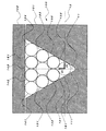
特許文献2に記載の方法に従い、クラッド径125μmのシングルモード光ファイバーのクラッドをフッ化水素水溶液にてエッチングし、クラッド外径39.0μmのものを選別した。これを7本束ね、エポキシ樹脂とともに、孔径118.0μm(クラッド外径39.0の3倍の117.0μmに1.0μmを加えた値)のセラミック製フェルールへ挿入し、樹脂を硬化させた。硬化完了後、出射端の光学研磨を行った。図16は、このようにして製造された、比較実施例1の端面近接光ファイバー1500の出射端面の光学顕微鏡写真(光ファイバーの非結束末端からも光照射)をトレースしたものである。一見すると7本の光ファイバーはきれいに整列しているように見えるが、詳細に観察すると、例えば矢印1521〜1525の指示する部位において、光ファイバー間およびフェルール内壁との間に、ランダムに、隙間が存在することが判る。従来の方法<孔に光ファイバー束を挿入>においては、この隙間をゼロにすることは不可能である。
(Comparative Example 1)
According to the method described in Patent Document 2, the clad of a single mode optical fiber having a clad diameter of 125 μm was etched with an aqueous hydrogen fluoride solution, and those having a clad outer diameter of 39.0 μm were selected. Seven of these were bundled together with an epoxy resin and inserted into a ceramic ferrule having a pore diameter of 118.0 μm (a value obtained by adding 1.0 μm to 117.0 μm, which is three times the cladding outer diameter of 39.0), and the resin was cured. . After the curing was completed, the output end was optically polished. FIG. 16 is a trace of the optical micrograph (light irradiation from the unbound end of the optical fiber) of the exit end face of the end face proximity
比較実施例1の端面近接光ファイバー(結束部分を含め全長1m)の透過損失を測定した一例を表3に示す。通常の光ファイバーであれば、長さ1mの透過損失は0.00dBに限りなく近い。比較実施例1の端面近接光ファイバーにおいては、長さ1mにもかかわらず、1dBを超える透過損失が観測された。これは、結束部分の光ファイバーがエポキシ樹脂の硬化収縮または光ファイバーの捻れによって、微細な屈曲を起こしていることに起因するものと推測される。光ファイバーの周辺に<隙間>が存在することが、このような不具合の根本原因である。 Table 3 shows an example in which the transmission loss of the end face proximity optical fiber of Comparative Example 1 (total length of 1 m including the bundled portion) was measured. In the case of a normal optical fiber, the transmission loss of 1 m in length is as close as possible to 0.00 dB. In the end face proximity optical fiber of Comparative Example 1, a transmission loss exceeding 1 dB was observed despite the length of 1 m. This is presumably due to the fact that the optical fiber in the bundling portion is slightly bent due to curing shrinkage of the epoxy resin or twisting of the optical fiber. The existence of <gap> around the optical fiber is the root cause of such problems.
比較実施例1の端面近接光ファイバーの結束側端面から出射するビームの進行方向が所定の直進方向から傾いている角度を測定した結果(例)を表4に示す。一部のファイバーにおいて、1度を超える大きな偏向が観察された。これは、当該光ファイバーの出射端面近傍における光ファイバーの屈曲および/または出射端面研磨の不備によるものと推測される。いずれにしても、光ファイバーの周辺に<隙間>が存在することが、このような不具合の根本原因となることは言うまでもない。 Table 4 shows the results (examples) of measuring the angle at which the traveling direction of the beam emitted from the end surface near the end face of the comparative example 1 is inclined from the predetermined straight direction. In some fibers, a large deflection of more than 1 degree was observed. This is presumed to be due to incomplete bending of the optical fiber and / or polishing of the outgoing end face in the vicinity of the outgoing end face of the optical fiber. In any case, needless to say, the existence of <gap> around the optical fiber is the root cause of such a malfunction.
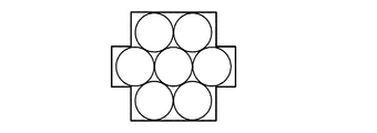
[第2の実施の形態]
図2は本発明の第2の実施の形態の端面近接多芯光ファイバー200の概略構成図であり、下側W字型溝基板201に設けられた第1のV字型断面の案内溝21に光ファイバー211を、隣接する第2のV字型断面の案内溝22に光ファイバー212を載置し、その上に第1の実施の形態と同様に光ファイバー221〜223、231〜234および上側平面基板202のすべてが組み立てられた状態を表している。
[Second Embodiment]
FIG. 2 is a schematic configuration diagram of the end-surface proximity multicore
2つのV字型断面の案内溝21と22は、合わせてW字型断面の案内溝を形成している。
The two V-shaped
最初に切削されて形成される第1のV字型断面の案内溝21に隣接して、第2のV字型断面の案内溝22を形成することは容易であるため、本発明の第1の実施の形態における第1層の光ファイバー111をダミーファイバーとして使用する場合は、本発明の第2の実施の形態の下側W字型溝基板201を採用することで、ダミーファイバーを削減することがきる。
Since it is easy to form the second V-shaped cross-section guide
(比較実施例2)
本発明の第1の実施の形態におけるV字型断面の案内溝の代わりに、矩形の案内溝を用いる方法について比較すると、図3に例示する場合、第1層に載置する光ファイバー311は、案内壁351,352,353の内、底面の案内壁352を必須として、光ファイバー外径の公差を考慮すると、案内壁351または353の、どちらか1つとしか接触できず、結果的に、載置位置を特定することはできない。
(Comparative Example 2)
Compared to the method using a rectangular guide groove instead of the V-shaped cross-section guide groove in the first embodiment of the present invention, when illustrated in FIG. 3, the
更に、第2層以降においては、各層の両端に位置する光ファイバー321,322,331,333,341,344は、矩形の案内壁、例えば361および362の他、下層の光ファイバー311の側面と接触する可能性があり、結果的に、載置位置を特定することはできない。
Further, in the second and subsequent layers, the
以上のような、幾何学的考察に加え、V字型断面の溝を掘削するよりも、矩形断面の溝を掘削することは容易でない。これは、切削で生じた屑をV字型断面では2つの壁に沿って左右対称に排出可能であることに対し、矩形断面の切削では、底辺で発生した切削屑を排出する方向が定まらず、切削治具の左右の位置が不定期に変動しやすい、という実施上の制約である。 In addition to the above geometrical considerations, it is not easy to excavate a rectangular cross-section groove than to excavate a V-shaped cross-section groove. This is because scrap generated by cutting can be discharged symmetrically along two walls in a V-shaped cross section, but in the cutting of a rectangular section, the direction of discharging the cutting scrap generated at the bottom is not fixed. This is a practical restriction that the left and right positions of the cutting jig are likely to fluctuate irregularly.
(比較実施例3)
本発明の第1の実施の形態におけるV字型断面の案内溝の代わりに、矩形の案内溝を用いる方法の、もう1つの可能性について比較すると、図6に例示する場合、第1層に載置する光ファイバー611および612は、各々、案内壁641と642、および同643と642の<2つ>のみで位置が決定される。しかしながら、第2層以降では、比較実施例2の場合と同様な制約が生じる。
(Comparative Example 3)
When comparing another possibility of the method using a rectangular guide groove instead of the V-shaped cross-section guide groove in the first embodiment of the present invention, in the case illustrated in FIG. The positions of the
いずれにしても、本発明のV字ないしW字型断面の案内壁に比べ、矩形の案内壁は切削加工の面において利点がない。 In any case, the rectangular guide wall has no advantage in terms of cutting as compared with the guide wall having a V-shaped or W-shaped cross section of the present invention.
[第3の実施の形態]
図4は、本発明の第3の実施の形態の端面近接多芯光ファイバー400の概念構成図である。
[Third Embodiment]
FIG. 4 is a conceptual configuration diagram of an end-surface proximity multicore
本発明の第1および第2の実施の形態では、下側基板に対して接着される上側基板は平面であったが、本発明の第3の実施の形態における下側基板401に対向する上側基板402は同一の断面を有している。
In the first and second embodiments of the present invention, the upper substrate bonded to the lower substrate is a flat surface, but the upper substrate facing the
上側基板402の案内溝は、本発明の第3の実施の形態の端面近接多芯光ファイバーの載置が完了した後、端面研磨に際しての剛性を高めるために載置されるものである。
The guide groove of the
即ち、第3層の光ファイバー431,432,433の上に第4層の光ファイバー441,442、次いで第5層の光ファイバー451を載置するには、下層の光ファイバー側面を基準とすれば良い。しかるに、結束された光ファイバー末端を光学研磨するにあたっては、個々の光ファイバーを高い剛性で保持する必要がある。本実施の形態における上側V字型溝基板402はこの目的に最も適するものである。
That is, in order to place the fourth-layer
第5層の光ファイバー451を載置した後、上側V字型溝基板402を載置し、下側V字型溝基板401と既に載置された光ファイバーと接着することで、端面近接多芯光ファイバー400の端面研磨に際して、全体の剛性を高めることができる。
After placing the optical fiber 451 of the fifth layer, the upper V-shaped
[第4の実施の形態]
図5は、本発明の第4の実施の形態の端面近接多芯光ファイバー500の概念構成図である。
[Fourth Embodiment]
FIG. 5 is a conceptual configuration diagram of an end-surface proximity multicore
本発明の第1および第2の実施の形態では、下側基板に対して接着される上側基板は平面であったが、本発明の第4の実施の形態における下側基板501に対向する上側基板502は同一の断面を有している。
In the first and second embodiments of the present invention, the upper substrate bonded to the lower substrate is a flat surface, but the upper substrate facing the
上側基板502の案内溝は、本発明の第4の実施の形態の端面近接多芯光ファイバーの載置が完了した後、端面研磨に際しての剛性を高めるために載置されるものである。
The guide groove of the
即ち、第2層の光ファイバー521,522,523の上に第3層の光ファイバー531および532を載置するには、下層の光ファイバー側面を基準とすれば良い。しかるに、結束された光ファイバー末端を光学研磨するにあたっては、個々の光ファイバーを高い剛性で保持する必要がある。本実施の形態における上側W字型溝基板502はこの目的に最も適するものである。
That is, in order to place the third-layer
第3層の光ファイバー531および532を載置した後、上側W字型溝基板502を載置し、下側V字型溝基板501と既に載置された光ファイバーと接着することで、端面近接多芯光ファイバー500の端面研磨に際して、全体の剛性を高めることができる。
After the third-layer
本発明の第4の実施の形態では、結束される光ファイバーの一端だけでなく、結束される光ファイバー部分に隣接し、例えば、クラッド径が大きくなる部分(即ち、クラッドがエッチングされていない部分)および、クラッドが被覆されている部分をも考慮した下側基板について、以下に記述する。 In the fourth embodiment of the present invention, not only one end of an optical fiber to be bundled, but also a portion adjacent to the optical fiber portion to be bundled, for example, a clad diameter becomes large (that is, a portion where the clad is not etched) and The lower substrate taking into account the portion coated with the clad will be described below.
いうまでもなく、クラッド径を40μm以下にエッチングした光ファイバーは非常に脆弱なもので、破損しやすい。また、簡単に屈曲し、光透過損失を招く。これらの不都合を避けるためには、被覆された光ファイバー部分から、被覆を除いた光ファイバー部分(クラッド径の大きい部分)を経由し、光ファイバー結束部分までを、緩やかな曲線で配置し、固定する必要がある。そのため、被覆された光ファイバー部分は、例えば、図7に示すような、余裕のある固定溝で緩やかに結束・固定することが好適である。 Needless to say, an optical fiber etched with a cladding diameter of 40 μm or less is very fragile and easily damaged. Moreover, it bends easily and causes a light transmission loss. In order to avoid these inconveniences, it is necessary to arrange and fix the optical fiber part from the coated optical fiber part through the optical fiber part excluding the coating (the part with the large cladding diameter) to the optical fiber bundling part with a gentle curve. is there. For this reason, it is preferable that the coated optical fiber portion is gently bound and fixed with a fixing groove having a margin as shown in FIG. 7, for example.
また、被覆を除去した光ファイバーをエッチングすることなく、通常のクラッド径125μmのまま、W字型案内溝を設けた基板で載置する例を図8aから図8dに示す。図8cおよび図8dに示す端面近接多芯光ファイバーにおいて、下側W字型溝基板801の上面、および上側W字型溝基板802の光学研磨面810に対する裏面側における網線で示した部分は、硬化収縮のない紫外線硬化樹脂で、むき出しのクラッド部分を保護・固定したものである。
Further, FIGS. 8a to 8d show examples of mounting on a substrate provided with a W-shaped guide groove with an ordinary cladding diameter of 125 μm without etching the coated optical fiber. 8c and 8d, the portion indicated by the mesh line on the upper surface of the lower W-shaped
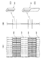
図9は、本発明の第4の実施の形態の端面近接多芯光ファイバーに用いられる上側W字型溝基板902と下側W字型溝基板901を石英基板上に複数形成した後、切り出す製法を表す概念図である。特に、図9(A)は切り出す前の平面図であり、図9(B)は切り出し前の(A)の側面図であり、図9(C)は切り出し後の上側W字型溝基板の斜視図であり、図9(D)は切り出し後の下側W字型溝基板の斜視図である。また、図10は、本発明の第4の実施の形態の端面近接多芯光ファイバーに用いられる上側W字型溝基板と下側W字型溝基板を石英基板上に複数形成した構造の一例の斜視図である。大きな石英基板の所定の位置に、被覆された光ファイバーを載置する部分と被覆のない光ファイバーを載置するW字型案内溝910を切削加工した後、図9(A)に示す一点鎖線で示す個所で切り離し、更に、上側W字型溝基板802と下側W字型溝基板801を、図9(A)に示す一点鎖線で切り離すことにより、高い精度で、図9(C)に示す上側W字型溝基板802と図9(D)に素雌下側W字型溝基板801とを1単位として、複数単位のW字型溝基板を作成することができる。
FIG. 9 shows a manufacturing method in which a plurality of upper W-shaped groove substrates 902 and lower W-shaped groove substrates 901 used in the end-surface proximity multicore optical fiber according to the fourth embodiment of the present invention are formed on a quartz substrate and then cut out. It is a conceptual diagram showing. 9A is a plan view before cutting, FIG. 9B is a side view of FIG. 9A before cutting, and FIG. 9C is an upper W-shaped groove substrate after cutting. FIG. 9D is a perspective view of the lower W-shaped groove substrate after cutting. FIG. 10 shows an example of a structure in which a plurality of upper W-shaped groove substrates and lower W-shaped groove substrates used in the end-surface proximity multicore optical fiber according to the fourth embodiment of the present invention are formed on a quartz substrate. It is a perspective view. After cutting a portion where a coated optical fiber is placed and a W-shaped guide groove 910 where an uncoated optical fiber is placed at a predetermined position on a large quartz substrate, this is shown by a one-dot chain line shown in FIG. Further, the upper W-shaped
[第5の実施の形態]
図11は、本発明の第4の実施の形態の端面近接多芯光ファイバー1001に隣接して設けられた2筋のV字型断面の案内溝1011および1012にダミーファイバーを載置することで、下側および上側のW字型案内溝基板の接合を、より確実に行うための、本発明の第5の実施の形態を表したものである。
[Fifth Embodiment]
FIG. 11 shows a dummy fiber placed in
図11に示すような端面形状を採用することで、端面研磨の際の剛直性を担保し、優れた端面研磨精度を達成することができる。 By adopting the end face shape as shown in FIG. 11, it is possible to ensure rigidity during the end face polishing and achieve excellent end face polishing accuracy.
[第6の実施の形態]
図12は本発明の第6の実施の形態の端面近接多芯光ファイバーの概念構成図である。ここで、下側基板と上側基板については案内溝部分のみ表示している。
[Sixth Embodiment]
FIG. 12 is a conceptual configuration diagram of an end-surface proximity multicore optical fiber according to the sixth embodiment of the present invention. Here, only the guide groove portion is shown for the lower substrate and the upper substrate.
本発明の第6の実施の形態においては、下側基板に7筋のV字型断面案内溝を設け、第1層に7本、第2層に8本、第3層に9本、第4層に8本、第5層に7本、合計39本を結束したものである。これを用いることで、例えば、熱レンズ方式1×7光制御光スイッチを3系列独立に束ねた動作が可能である。
In the sixth embodiment of the present invention, seven lower V-shaped cross-sectional guide grooves are provided on the lower substrate, seven on the first layer, eight on the second layer, nine on the third layer, A total of 39 bundles, 8 on the 4th layer and 7 on the 5th layer. By using this, for example, an operation in which three
[第7の実施の形態]
図13は本発明の第7の実施の形態の端面近接多芯光ファイバーの概念構成図である。本発明の第4の実施の形態の端面近接多芯光ファイバー3組を、並列配置したものである。
[Seventh Embodiment]
FIG. 13 is a conceptual configuration diagram of an end-face proximity multicore optical fiber according to a seventh embodiment of the present invention. Three sets of end-surface proximity multicore optical fibers according to the fourth embodiment of the present invention are arranged in parallel.
本発明の端面近接多芯光ファイバーおよびその製造方法は、光通信分野および光情報処理分野において有効に用いることができる。 The end-surface proximity multicore optical fiber and the manufacturing method thereof according to the present invention can be effectively used in the fields of optical communication and optical information processing.
本発明の端面近接多芯光ファイバーを用いることで、例えば、個々のシングルモード光ファイバーが1本ずつ独立してなる端面近接多芯光ファイバーを用い、1本から制御光を、隣接するもう1本から信号光を出射させることによって、熱レンズ方式光制御式光路偏向光路偏向スイッチを極めて効率的に動作させることができる。 By using the end-face proximity multicore optical fiber of the present invention, for example, an end-face proximity multicore optical fiber in which each single mode optical fiber is independent one by one is used, control light is transmitted from one, and signal is transmitted from the other adjacent one. By emitting the light, the thermal lens type light control type optical path deflection optical path deflection switch can be operated extremely efficiently.
11,21,23 V字型断面の案内溝およびその中心線(y軸)、12 案内溝11の中心線に直交し図1の平面に平行な線(x軸)、14 V字型断面の案内溝に載置される光ファイバーの中心軸(z軸)、22 W字型断面の案内溝の中心線、100 本発明の第1の実施の形態の端面近接多芯光ファイバー、101 下側V字型溝基板、102,202,302,602 上側平面基板、105 光ファイバー押しつけ治具の先端部分、106 光ファイバー押しつけ治具、111 第1層(最下層)に載置された光ファイバー、121,122 第2層に載置された光ファイバー、131〜133 第3層に載置された光ファイバー、141〜144 第4層に載置された光ファイバー、151,152 V字型断面の案内溝11を構成する案内壁、161,261,391 上側平面基板の平面壁、200 本発明の第2の実施の形態の端面近接多芯光ファイバー、201 下側W字型溝基板、211,212 第1層(最下層)に載置された光ファイバー、221〜223 第2層に載置された光ファイバー、231〜234 第3層に載置された光ファイバー、251〜254 W字型断面の案内溝を構成する案内壁、300 比較実施例1の端面近接多芯光ファイバー、301 下側角型溝基板、311 第1層(最下層)に載置された光ファイバー、321,322 第2層に載置された光ファイバー、331〜333 第3層に載置された光ファイバー、341〜344 第4層に載置された光ファイバー、351〜353,361〜364,371〜374,381〜384 角型断面の案内溝を構成する案内壁、400 本発明の第3の実施の形態の端面近接多芯光ファイバー、401 下側V字型溝基板、402 上側V字型溝基板、411 第1層(最下層)に載置された光ファイバー、421,422 第2層に載置された光ファイバー、431〜433 第3層に載置された光ファイバー、441,442 第4層に載置された光ファイバー、451 第5層に載置された光ファイバー、461,462,471,472 V字型断面の案内溝を構成する案内壁、500,800 本発明の第4の実施の形態の端面近接多芯光ファイバー、501,801,901 下側W字型溝基板、502,802,902 上側W字型溝基板、511,512 第1層(最下層)に載置された光ファイバー、521〜523 第2層に載置された光ファイバー、531,532 第3層に載置された光ファイバー、541〜544,551〜554 W字型断面の案内溝を構成する案内壁、600 比較実施例2の端面近接多芯光ファイバー、601 下側角型溝基板、611,612 第1層(最下層)に載置された光ファイバー、621〜623 第2層に載置された光ファイバー、631〜634 第3層に載置された光ファイバー、641〜643,651〜654,661〜664 角型断面の案内溝を構成する案内壁、810 光学研磨面、910 W字型案内溝、1001 本発明の第5の実施の形態の端面近接多芯光ファイバーのファイバーバンドル部分、1011,1012 ダミーファイバーおよびV字型断面案内溝、1111,1112 光ファイバー111側面と案内壁151または152の接点を指示する矢印、1211 光ファイバー121側面と案内壁151の接点を指示する矢印、1212 光ファイバー121側面と光ファイバー111側面の接点を指示する矢印、1221 光ファイバー122側面と案内壁152の接点を指示する矢印、1222 光ファイバー122側面と光ファイバー111側面の接点を指示する矢印、1301 加工前の基板、1400 端面近接多芯光ファイバー結束装置、1401 光学基盤、1402 下側基板固定用架台、1403 光検出器用微動架台、1404,1405 架台、1406 光ファイバー押しつけ治具の微動機構、1410 下側基板、1420 レーザー光源、1421 光パワーメーター受光器またはビームプロファイラー受光器、1430 接着剤注入ノズル、1440 案内溝とそこに載置される光ファイバーの間の隙間、1441 光ファイバー結束部分、1442 光ファイバークラッド径拡大部分、1443 光ファイバー被覆部分、1451,1452 光ファイバー結束部分用押しつけ治具、1453 光ファイバークラッド径拡大部分用押しつけ治具、1454 光ファイバー被覆部分用押しつけ治具、1461,1462,1463,1464 光ファイバー押しつけ治具の先端部分、1470 顕微鏡、1480 紫外線硬化樹脂用紫外線光源、1500 比較実施例1の端面近接光ファイバー、1501 セラミック製フェルールの孔、1510 シングルモード光ファイバーのコア部分、1511 シングルモード光ファイバーのクラッド部分、1521〜1525 光ファイバー周辺の隙間を示す矢印。 11, 21, 23 V-shaped cross-section guide groove and its center line (y-axis), 12 A line perpendicular to the center line of the guide groove 11 and parallel to the plane of FIG. 1 (x-axis), 14 V-shaped cross-section The center axis (z axis) of the optical fiber placed in the guide groove, the center line of the guide groove having a 22 W-shaped cross section, 100 the end face proximity multicore optical fiber according to the first embodiment of the present invention, 101, the lower V-shape Ditch substrate, 102, 202, 302, 602 Upper plane substrate, 105 Optical fiber pressing jig tip part, 106 Optical fiber pressing jig, 111 Optical fiber placed on first layer (lowermost layer), 121, 122 2nd Optical fiber placed on the layer, 131-133 optical fiber placed on the third layer, 141-144 optical fiber placed on the fourth layer, 151,152 V-shaped cross-section guide groove 11 Guide wall, 161, 261, 391 Planar wall of upper planar substrate, 200 End face proximity multi-core optical fiber according to the second embodiment of the present invention, 201 Lower W-shaped groove substrate, 211, 212 First layer (lowermost layer) ), An optical fiber placed on the second layer, an optical fiber placed on the 231 to 234 third layer, a guide wall constituting a guide groove having a 251 to 254 W-shaped cross section, 300 End face proximity multi-core optical fiber of Comparative Example 1, 301 lower square groove substrate, 311 optical fiber placed on first layer (lowermost layer), 321 and 322 optical fiber placed on second layer, 331- 333 Optical fiber placed on the third layer, 341 to 344 Optical fiber placed on the fourth layer, 351 to 353, 361 to 364, 371 to 374, 381 to 384 Guide wall that forms a guide groove with a square cross section, 400 Multi-core optical fiber near the end face according to the third embodiment of the present invention, 401 Lower V-shaped groove substrate, 402 Upper V-shaped groove substrate, 411 First layer An optical fiber placed on the lowermost layer, 421, 422 an optical fiber placed on the second layer, 431-433 an optical fiber placed on the third layer, 441, 442 an optical fiber placed on the fourth layer, 451, an optical fiber placed on the fifth layer, 461, 462, 471, 472, guide walls constituting guide grooves having a V-shaped cross section, 500, 800, end-face proximity multicore optical fibers according to the fourth embodiment of the present invention, 501, 801, 901 Lower W-shaped groove substrate, 502, 802, 902 Upper W-shaped groove substrate, 511, 512 Optical fiber placed on the first layer (lowermost layer), 521-523 Optical fiber placed in two layers, 531 and 532 Optical fiber placed in the third layer, guide walls constituting guide grooves of 541 to 544 and 551 to 554 W-shaped cross section, 600 End face proximity of comparative example 2 Multi-core optical fiber, 601 Lower square groove substrate, 611, 612 Optical fiber placed on first layer (lowermost layer), 621-623 Optical fiber placed on second layer, 631-634 Mounted on third layer Optical fiber, 641 to 643, 651 to 654, 661 to 664, guide wall constituting a guide groove having a square cross section, 810 optical polishing surface, 910 W-shaped guide groove, 1001 fifth embodiment of the present invention Fiber bundle portion of multi-core optical fiber near end face, 1011, 1012 dummy fiber and V-shaped cross-section guide groove, 1111, 1112 optical fiber 11 indicates the contact point between the side surface and the guide wall 151 or 152, 1211 indicates the contact point between the optical fiber 121 side surface and the guide wall 151, 1212 indicates the contact point between the optical fiber 121 side surface and the optical fiber 111 side surface, and 1221 the optical fiber 122 side surface Arrow indicating the contact point of the guide wall 152, arrow indicating the contact point between the 1222 side surface of the optical fiber 122 and the side surface of the optical fiber 111, 1301 substrate before processing, 1400 end face proximity multi-core optical fiber bundling device, 1401 optical substrate, 1402 for fixing the lower substrate Base, 1403 Fine detector for optical detector, 1404, 1405 Base, 1406 Fine movement mechanism of optical fiber pressing jig, 1410 Lower substrate, 1420 Laser light source, 1421 Optical power meter receiver or beam profiler , 1430 Adhesive injection nozzle, 1440 Gap between guide groove and optical fiber placed thereon, 1441 Optical fiber bundling portion, 1442 Optical fiber clad diameter enlarged portion, 1443 Optical fiber covering portion, 1451, 1452 Pressing jig for optical fiber bundling portion , 1453 Optical fiber clad diameter enlarged portion pressing jig, 1454 Optical fiber coating portion pressing jig, 1461, 1462, 1463, 1464 Optical fiber pressing jig tip part, 1470 Microscope, 1480 Ultraviolet light source for UV curable resin, 1500 Comparative implementation End face proximity optical fiber of Example 1, 1501 Ceramic ferrule hole, 1510 Core part of single mode optical fiber, 1511 Clad part of single mode optical fiber, 1521 ˜1525 An arrow indicating a gap around the optical fiber.
Claims (1)
前記基板固定用架台上の溝基板の案内溝に順次光ファイバーを配置する1つ以上の光ファイバー押しつけ治具と、
前記案内溝内に光ファイバーを2段以上積み重ねるために前記押しつけ治具を微動移動可能に駆動させる微動機構と、
光ファイバーの結束端側に設けられ、光ファイバーの非結束端に接続されるレーザー光源から出力された光に対する光ファイバーの光透過特性を測定する受光測定器と、
前記光ファイバーの結束端側に設けられ、前記案内溝と光ファイバーとの隙間に接着剤を注入する注入ノズルと、
を有し、
前記受光測定器の出力に応じて、微動機構による1つ以上の光ファイバー押しつけ治具の押しつけ分布を調整し、注入ノズルから注入された接着剤により1つ以上の光ファイバーを案内溝内に固定することを特徴とする端面近接多芯光ファイバーの製造装置。
A substrate fixing base on which a groove substrate on which one or more guide grooves are formed is placed;
One or more optical fiber pressing jigs for sequentially arranging optical fibers in the guide grooves of the groove substrate on the substrate fixing base;
A fine movement mechanism for driving the pressing jig so as to be capable of fine movement to stack two or more optical fibers in the guide groove;
A light receiving measuring device that is provided on the binding end side of the optical fiber and measures the light transmission characteristics of the optical fiber with respect to the light output from the laser light source connected to the non-binding end of the optical fiber;
An injection nozzle that is provided on the binding end side of the optical fiber and injects an adhesive into a gap between the guide groove and the optical fiber;
Have
The distribution of pressing of one or more optical fiber pressing jigs by the fine movement mechanism is adjusted according to the output of the light receiving measuring device, and one or more optical fibers are fixed in the guide groove by the adhesive injected from the injection nozzle. An end face proximity multi-core optical fiber manufacturing apparatus.
Priority Applications (1)
| Application Number | Priority Date | Filing Date | Title |
|---|---|---|---|
| JP2014126248A JP5755783B2 (en) | 2014-06-19 | 2014-06-19 | End-face proximity multicore optical fiber manufacturing equipment |
Applications Claiming Priority (1)
| Application Number | Priority Date | Filing Date | Title |
|---|---|---|---|
| JP2014126248A JP5755783B2 (en) | 2014-06-19 | 2014-06-19 | End-face proximity multicore optical fiber manufacturing equipment |
Related Parent Applications (1)
| Application Number | Title | Priority Date | Filing Date |
|---|---|---|---|
| JP2011196852A Division JP5611160B2 (en) | 2011-09-09 | 2011-09-09 | End face proximity multi-core optical fiber manufacturing method and apparatus |
Publications (2)
| Publication Number | Publication Date |
|---|---|
| JP2014194581A true JP2014194581A (en) | 2014-10-09 |
| JP5755783B2 JP5755783B2 (en) | 2015-07-29 |
Family
ID=51839818
Family Applications (1)
| Application Number | Title | Priority Date | Filing Date |
|---|---|---|---|
| JP2014126248A Expired - Fee Related JP5755783B2 (en) | 2014-06-19 | 2014-06-19 | End-face proximity multicore optical fiber manufacturing equipment |
Country Status (1)
| Country | Link |
|---|---|
| JP (1) | JP5755783B2 (en) |
Cited By (1)
| Publication number | Priority date | Publication date | Assignee | Title |
|---|---|---|---|---|
| JP2018500984A (en) * | 2014-12-11 | 2018-01-18 | コーニンクレッカ フィリップス エヌ ヴェKoninklijke Philips N.V. | Cable loop detection mechanism for improved MRI safety |
Citations (3)
| Publication number | Priority date | Publication date | Assignee | Title |
|---|---|---|---|---|
| JPS61248010A (en) * | 1985-04-23 | 1986-11-05 | ブリテイシユ・テレコミユニケ−シヨンズ・パブリツク・リミテツド・カンパニ | Structure and method for terminating optical fiber |
| JPH0894864A (en) * | 1994-04-08 | 1996-04-12 | Olympus Optical Co Ltd | Image fiber and its production |
| JP2002031726A (en) * | 2001-05-14 | 2002-01-31 | Dainippon Screen Mfg Co Ltd | Optical fiber array |
-
2014
- 2014-06-19 JP JP2014126248A patent/JP5755783B2/en not_active Expired - Fee Related
Patent Citations (3)
| Publication number | Priority date | Publication date | Assignee | Title |
|---|---|---|---|---|
| JPS61248010A (en) * | 1985-04-23 | 1986-11-05 | ブリテイシユ・テレコミユニケ−シヨンズ・パブリツク・リミテツド・カンパニ | Structure and method for terminating optical fiber |
| JPH0894864A (en) * | 1994-04-08 | 1996-04-12 | Olympus Optical Co Ltd | Image fiber and its production |
| JP2002031726A (en) * | 2001-05-14 | 2002-01-31 | Dainippon Screen Mfg Co Ltd | Optical fiber array |
Cited By (1)
| Publication number | Priority date | Publication date | Assignee | Title |
|---|---|---|---|---|
| JP2018500984A (en) * | 2014-12-11 | 2018-01-18 | コーニンクレッカ フィリップス エヌ ヴェKoninklijke Philips N.V. | Cable loop detection mechanism for improved MRI safety |
Also Published As
| Publication number | Publication date |
|---|---|
| JP5755783B2 (en) | 2015-07-29 |
Similar Documents
| Publication | Publication Date | Title |
|---|---|---|
| US9784930B2 (en) | Optical interface device having a curved waveguide using laser writing and methods of forming | |
| JP4577376B2 (en) | Manufacturing method of optical waveguide | |
| WO2012172906A1 (en) | Optical connection member, optical connection structure, and method for producing optical connection member | |
| JP2007041222A (en) | Optical coupler and optical connector | |
| US20140294339A1 (en) | Compact optical fiber splitters | |
| US10025040B2 (en) | Connector for multilayered optical waveguide | |
| JP5611160B2 (en) | End face proximity multi-core optical fiber manufacturing method and apparatus | |
| JP5673223B2 (en) | OPTICAL FIBER COMPONENT AND ITS MANUFACTURING METHOD, OPTICAL FIBER / LENS SUBSTRATE ASSEMBLY AND ITS MANUFACTURING METHOD | |
| Yakabe et al. | Multi-channel single-mode polymer waveguide fabricated using the Mosquito method | |
| KR101760156B1 (en) | Optical collimator and optical connector using same | |
| US20220057579A1 (en) | Optical coupling device and method for manufacturing optical coupling device | |
| JP2014029386A (en) | Method for producing polymer waveguide array assembly of single mode | |
| JP5755783B2 (en) | End-face proximity multicore optical fiber manufacturing equipment | |
| US20220026641A1 (en) | Optical connector and optical connector manufacturing method | |
| US11966091B2 (en) | Multichannel optical coupler array | |
| JP6513583B2 (en) | Optical fiber side input / output device and method of manufacturing the same | |
| JP2012247545A (en) | Fan-out component for multi-core fiber | |
| JP4524390B2 (en) | Manufacturing method of optical connection device | |
| JP2005309092A (en) | Optical connector and its manufacturing method | |
| JP2002311270A (en) | Vertical transmission type optical waveguide and production method therefor | |
| JP3026477B2 (en) | Optical waveguide substrate | |
| JP3067109B1 (en) | Optical component and optical fiber terminal structure | |
| WO2016175126A1 (en) | Optical transmission module | |
| JPH08240738A (en) | Optical waveguide device and production therefor | |
| JP2008281695A (en) | Light guide and light guide substrate |
Legal Events
| Date | Code | Title | Description |
|---|---|---|---|
| A131 | Notification of reasons for refusal |
Free format text: JAPANESE INTERMEDIATE CODE: A131 Effective date: 20150303 |
|
| A521 | Written amendment |
Free format text: JAPANESE INTERMEDIATE CODE: A523 Effective date: 20150420 |
|
| TRDD | Decision of grant or rejection written | ||
| A01 | Written decision to grant a patent or to grant a registration (utility model) |
Free format text: JAPANESE INTERMEDIATE CODE: A01 Effective date: 20150519 |
|
| A61 | First payment of annual fees (during grant procedure) |
Free format text: JAPANESE INTERMEDIATE CODE: A61 Effective date: 20150527 |
|
| R150 | Certificate of patent or registration of utility model |
Ref document number: 5755783 Country of ref document: JP Free format text: JAPANESE INTERMEDIATE CODE: R150 |
|
| LAPS | Cancellation because of no payment of annual fees |