JP2014192517A - Magnetic device - Google Patents
Magnetic device Download PDFInfo
- Publication number
- JP2014192517A JP2014192517A JP2013069812A JP2013069812A JP2014192517A JP 2014192517 A JP2014192517 A JP 2014192517A JP 2013069812 A JP2013069812 A JP 2013069812A JP 2013069812 A JP2013069812 A JP 2013069812A JP 2014192517 A JP2014192517 A JP 2014192517A
- Authority
- JP
- Japan
- Prior art keywords
- substrate
- surface layer
- coil pattern
- heat
- coil
- Prior art date
- Legal status (The legal status is an assumption and is not a legal conclusion. Google has not performed a legal analysis and makes no representation as to the accuracy of the status listed.)
- Granted
Links
Images


Abstract
Description
本発明は、磁性体から成るコアと、コイルパターンが設けられた基板とを備えた、チョークコイルやトランスなどの磁気デバイスに関する。 The present invention relates to a magnetic device such as a choke coil or a transformer including a core made of a magnetic material and a substrate provided with a coil pattern.
たとえば、高電圧の直流をスイッチングして交流に変換した後、低電圧の直流に変換するスイッチング電源装置がある。このスイッチング電源装置には、チョークコイルやトランスなどの磁気デバイスが使用されている。 For example, there is a switching power supply device that converts a high-voltage direct current into a alternating current after switching to a low-voltage direct current. The switching power supply device uses a magnetic device such as a choke coil or a transformer.
たとえば、特許文献1〜7には、コイルの巻線が基板に形成されたコイルパターンから成る、磁気デバイスが開示されている。
For example,
特許文献1〜5および7では、磁性体から成るコアが、基板を貫通している。基板は、絶縁体から成り、複数の層を有している。各層には、コアの周囲に巻回されるように、コイルパターンが設けられている。異なる層のコイルパターン同士は、スルーホールなどで接続されている。コイルパターンやスルーホールは、銅などの導体から成る。
In
特許文献6では、基板が、一対の絶縁層と、該絶縁層に挟持された磁性体層とから構成されている。磁性体層には、導体から成るコイルパターンが形成されている。コイルパターンは、基板の板面や厚み方向に複数回巻回されている。 In Patent Document 6, the substrate is composed of a pair of insulating layers and a magnetic layer sandwiched between the insulating layers. A coil pattern made of a conductor is formed on the magnetic layer. The coil pattern is wound a plurality of times in the plate surface and thickness direction of the substrate.
特許文献1および4では、基板の各層で、コイルパターンの幅が部分的に異なっている。特許文献2および3では、基板の最も上にある外面層に設けられたコイルパターンの幅が、他の内層に設けられたコイルパターンの幅より太くなっている。特許文献5および7では、幅が細くて巻き数が多いコイルパターンが設けられた層と、幅が太くて巻き数が少ないコイルパターンが設けられた層が、それぞれ複数積層されている。また、特許文献7では、基板の最も上にある層と最も下にある層に、幅が細くて巻き数が多いコイルパターンが設けられている。特許文献6では、コイルパターンの幅が一定になっている。
In
コイルパターンに電流が流れると、コイルパターンが発熱し、基板の温度が上昇する。基板の放熱対策として、特許文献1では、コイルパターンを基板の各層のほぼ全域に広げている。特許文献3では、基板の各層のコイルパターンの一部の幅を広げて、放熱パターン部を設けている。特許文献6では、コイルパターンの内側に、磁性体層と下方の絶縁層とを貫通する伝熱用貫通導体を設け、基板の下面に伝熱用貫通導体と接続された放熱用導体層を設けている。
When a current flows through the coil pattern, the coil pattern generates heat and the substrate temperature rises. As a heat dissipation measure for the substrate, in
基板の各層において、コイルパターンの幅を細くすると、基板を大きくしなくても、コイルパターンの巻き数を多くして、コイルの所定の性能を達成することができる。しかし、コイルパターンの幅を細くするほど、直流抵抗が高くなるため、コイルパターンでの発熱量が多くなり、基板の温度が上昇して、特性の変動や性能の劣化を招いてしまう。 In each layer of the substrate, if the width of the coil pattern is reduced, the predetermined performance of the coil can be achieved by increasing the number of turns of the coil pattern without increasing the size of the substrate. However, as the width of the coil pattern is reduced, the direct current resistance is increased, so that the amount of heat generated in the coil pattern is increased, the temperature of the substrate is increased, and the characteristics are changed and the performance is deteriorated.
特に、大電流が流れる直流−直流変換装置(DC−DCコンバータ)などで使用される磁気デバイスでは、コイルパターンに大電流が流れるので、コイルパターンの幅が細すぎると、発熱量がより多くなって、所定の特性や性能が得られない。また、同一基板上に他のICチップなどの電子部品が実装されている場合、基板の温度が高くなると、電子部品の誤動作や破壊を生じるおそれがある。 In particular, in a magnetic device used in a DC-DC converter (DC-DC converter) or the like in which a large current flows, a large current flows in the coil pattern. Therefore, if the width of the coil pattern is too narrow, the amount of heat generated increases. Therefore, predetermined characteristics and performance cannot be obtained. In addition, when an electronic component such as another IC chip is mounted on the same substrate, the electronic component may malfunction or be destroyed when the temperature of the substrate becomes high.
本発明の課題は、複数の層に幅の異なるコイルパターンが設けられた基板の放熱性能を高めることである。 The subject of this invention is improving the thermal radiation performance of the board | substrate with which the coil pattern from which a width | variety differs was provided in several layers.
本発明による磁気デバイスは、磁性体から成るコアと、絶縁体から成り、コアが貫通する基板と、基板の所定の層に設けられた、導体から成るコイルパターンとを備え、基板の一方の外面層にあるコイルパターンの幅が、他の層にあるコイルパターンの幅より細く、一方の外面層側に放熱器が設けられている。 A magnetic device according to the present invention includes a core made of a magnetic material, a substrate made of an insulator, the substrate through which the core penetrates, and a coil pattern made of a conductor provided in a predetermined layer of the substrate, and one outer surface of the substrate The width of the coil pattern in the layer is narrower than the width of the coil pattern in the other layer, and a radiator is provided on one outer surface layer side.
このようにすると、基板の一方の外面層にあるコイルパターンにおいて、パターンの幅が細いために発熱量が多くなっても、該コイルパターンで発生した熱を、放熱器により効率良く放熱させることができる。また、他の層にあるコイルパターンにおいては、パターンの幅を太くすることで、発熱量を抑制できるとともに、該コイルパターンの表面から放熱させ易くすることができる。このため、複数の層に幅の異なるコイルパターンが設けられた基板の放熱性能を高めることができる。また、コイルパターンの発熱を許容することができる。 In this way, in the coil pattern on one outer surface layer of the substrate, even if the heat generation amount increases because the pattern width is narrow, the heat generated by the coil pattern can be efficiently dissipated by the radiator. it can. Moreover, in the coil pattern in another layer, by increasing the width of the pattern, the amount of generated heat can be suppressed, and heat can be easily radiated from the surface of the coil pattern. For this reason, the thermal radiation performance of the board | substrate with which the coil pattern from which a width | variety differs in several layers was provided can be improved. Moreover, heat generation of the coil pattern can be allowed.
また、本発明では、上記磁気デバイスにおいて、基板の一方の外面層にあるコイルパターンの巻き数は、他の層にあるコイルパターンの巻き数より多くてもよい。 In the present invention, in the above magnetic device, the number of turns of the coil pattern on one outer surface layer of the substrate may be larger than the number of turns of the coil pattern on the other layer.
また、本発明では、上記磁気デバイスにおいて、一方の外面層にあるコイルパターンを部分的に拡張することにより、当該一方の外面層に、導体から成る放熱部を設けてもよい。 In the present invention, in the above magnetic device, a heat radiation portion made of a conductor may be provided on the one outer surface layer by partially expanding a coil pattern on the one outer surface layer.
また、本発明では、上記磁気デバイスにおいて、基板は、表面と裏面にそれぞれ外面層が設けられ、コイルパターンは、基板の一方の外面層と他方の外面層にそれぞれ設けられていてもよい。 In the present invention, in the magnetic device, the substrate may be provided with outer surface layers on the front surface and the back surface, respectively, and the coil pattern may be provided on one outer surface layer and the other outer surface layer of the substrate, respectively.
また、本発明では、上記磁気デバイスにおいて、一方の外面層側に設けた放熱器が第1放熱器であり、他方の外面層側に第2放熱器をさらに設けてもよい。 In the present invention, in the magnetic device, the radiator provided on one outer surface layer side may be the first radiator, and the second radiator may be further provided on the other outer layer side.
さらに、本発明では、上記磁気デバイスにおいて、他方の外面層にあるコイルパターンと別体で、他方の外面層に設けられた導体から成る放熱パターンと、基板に設けられた導体から成り、一方の外面層にあるコイルパターンと他方の外面層にある放熱パターンとを接続する放熱用接続部と、をさらに備えてもよい。 Further, according to the present invention, in the above magnetic device, the coil device is separate from the coil pattern on the other outer surface layer, and is composed of a heat radiation pattern made of a conductor provided on the other outer surface layer, and a conductor provided on the substrate. You may further provide the thermal radiation connection part which connects the coil pattern in an outer surface layer, and the thermal radiation pattern in the other outer surface layer.
本発明の磁気デバイスによれば、複数の層に幅の異なるコイルパターンが設けられた基板の放熱性能を高めることができる。 According to the magnetic device of the present invention, it is possible to improve the heat dissipation performance of a substrate in which a plurality of layers are provided with coil patterns having different widths.
以下、本発明の実施形態につき、図面を参照しながら説明する。各図において、同一の部分または対応する部分には、同一符号を付してある。 Hereinafter, embodiments of the present invention will be described with reference to the drawings. In the drawings, the same or corresponding parts are denoted by the same reference numerals.
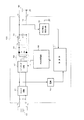
図1は、スイッチング電源装置100の構成図である。スイッチング電源装置100は、電気自動車(またはハイブリッドカー)用のDC−DCコンバータであり、高電圧の直流をスイッチングして交流に変換した後、低電圧の直流に変換する。以下で詳述する。
FIG. 1 is a configuration diagram of the switching
スイッチング電源装置100の入力端子T1、T2には、高電圧バッテリ50が接続されている。高電圧バッテリ50の電圧は、たとえばDC220V〜DC400Vである。入力端子T1、T2へ入力される高電圧バッテリ50の直流電圧Viは、フィルタ回路51でノイズが除去された後、スイッチング回路52へ与えられる。
A
スイッチング回路52は、たとえばFET(Field Effect Transistor:電界効果トランジスタ)を有する公知の回路からなる。スイッチング回路52では、PWM駆動部58からのPWM(Pulse Width Modulation:パルス幅変調)信号に基づいて、FETをオンオフさせて、直流電圧に対してスイッチング動作を行う。これにより、直流電圧が高周波のパルス電圧に変換される。
The
そのパルス電圧は、トランス53を介して、整流回路54へ与えられる。整流回路54は、一対のダイオードD1、D2によりパルス電圧を整流する。整流回路54で整流された電圧は、平滑回路55へ入力される。平滑回路55は、チョークコイルLおよびコンデンサCのフィルタ作用により整流電圧を平滑し、低電圧の直流電圧として出力端子T3、T4へ出力する。この直流電圧により、出力端子T3、T4に接続された低圧バッテリ60が、たとえばDC12Vに充電される。低圧バッテリ60の直流電圧は、図示しない各種の車載電装品へ供給される。
The pulse voltage is given to the
また、平滑回路55の出力電圧Voは、出力電圧検出回路59により検出された後、PWM駆動部58へ出力される。PWM駆動部58は、出力電圧Voに基づいてPWM信号のデューティ比を演算し、該デューティ比に応じたPWM信号を生成して、スイッチング回路52のFETのゲートへ出力する。これにより、出力電圧を一定に保つためのフィードバック制御が行なわれる。
The output voltage Vo of the smoothing
制御部57は、PWM駆動部58の動作を制御する。フィルタ回路51の出力側には、電源56が接続されている。電源56は、高電圧バッテリ50の電圧を降圧し、制御部57に電源電圧(たとえばDC12V)を供給する。
The
上記のスイッチング電源装置100において、平滑回路55のチョークコイルLとして、後述の磁気デバイス1、1’が用いられる。チョークコイルLには、たとえばDC150Aの大電流が流れる。チョークコイルLの両端には、電力入出力用のリード端子6i、6oが設けられている。
In the switching
次に、第1実施形態による磁気デバイス1の構造を、図2〜図4を参照しながら説明する。
Next, the structure of the
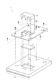
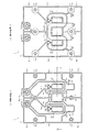
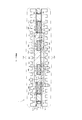
図2は、磁気デバイス1の分解斜視図である。図3は、磁気デバイス1の基板3の各層の平面図である。図4は、磁気デバイス1の断面図であって、図3のX−X断面を示している。
FIG. 2 is an exploded perspective view of the
図2に示すように、コア2a、2bは、E字形の上コア2aとI字形の下コア2bの、2個1対で構成されている。コア2a、2bは、フェライトまたはアモルファス金属などの磁性体から成る。
As shown in FIG. 2, the
上コア2aは、下方へ突出するように、3つの凸部2m、2L、2rを有している。中央の凸部2mに対して、左側の凸部2Lと右側の凸部2rの方が、突出量が多くなっている。
The
図4に示すように、上コア2aの左右の凸部2L、2rの下端を、下コア2bの上面に密着させて、該コア2a、2bは組み合わされる。この状態では、直流重畳特性を高めるため、上コア2aの凸部2mと下コア2bの上面には所定の大きさの隙間が設けられている。これにより、磁気デバイス1(チョークコイルL)に大電流を流したときでも、所定のインダクタンスを実現することができる。コア2a、2b同士は、図示しないねじや金具などの固定手段により固定される。
As shown in FIG. 4, the lower ends of the left and right
下コア2bは、ヒートシンク10の上側に設けられた凹部10k(図2)に嵌め込まれる。ヒートシンク10の下側には、フィン10fが設けられている。ヒートシンク10は、金属製であり、本発明の「放熱器」の一例である。
The
基板3は、絶縁体から成る薄板状の基材の各層に、厚みの厚い銅箔(導体)でパターンが形成された厚銅箔基板から構成されている。本実施形態では、基板3に他の電子部品や回路が設けられていないが、実際に磁気デバイス1を図1のスイッチング電源装置100で使用する場合、同一基板上に磁気デバイス1とスイッチング電源装置100の他の電子部品や回路が設けられる(後述の磁気デバイス1’も同様)。
The board |
基板3の裏面(図2および図4で下面)には、図3(a)に示すような裏側外面層L1が設けられている。基板3の表面(図2および図4で上面)には、図3(b)に示すような表側外面層L2が設けられている。つまり、基板3は、回路を形成可能な上下2層L1、L2を有している。裏側外面層L1は、本発明の「一方の外面層」の一例である。表側外面層L2は、本発明の「他方の外面層」の一例である。
On the back surface of the substrate 3 (the lower surface in FIGS. 2 and 4), a back-side outer surface layer L1 as shown in FIG. 3A is provided. A front-side outer surface layer L2 as shown in FIG. 3B is provided on the surface of the substrate 3 (upper surface in FIGS. 2 and 4). That is, the
基板3には、複数の開口部3m、3L、3rが設けられている。各開口部3m、3L、3rには、図2〜図4に示すように、上コア2aの各凸部2m、2L、2rがそれぞれ挿入される。これにより、上コア2aは基板3を貫通する。
The
また、基板3には複数の貫通孔3aが設けられている。各貫通孔3aには、図2に示すように、各ねじ11が挿入される。基板3の裏面をヒートシンク10の上面(フィン10fと反対側)と対向させる。そして、各ねじ11を基板3の表面側から各貫通孔3aに貫通させて、ヒートシンク10の各ねじ孔10aに螺合する。これにより、図4に示すように、基板3の裏側外面層L1側にヒートシンク10が近接状態で固定される。基板3とヒートシンク10の間には、伝熱性を有する絶縁シート12が挟み込まれる。
The
図3に示すように、基板3には、複数のスルーホール8i、8o、9a、9bが形成されている。これらのスルーホール8i、8o、9a、9bは、異なる層L1、L2にあるパターン4a〜4c同士を接続する。
As shown in FIG. 3, the
詳しくは、スルーホール8iは、裏側外面層L1のパターン4aと表側外面層L2を接続する。スルーホール8oは、裏側外面層L1のパターン4bと表側外面層L2を接続する。スルーホール9aは裏側外面層L1のパターン4aと表側外面層L2のパターン4cを接続する。スルーホール9bは裏側外面層L1のパターン4bと表側外面層L2のパターン4cを接続する。
Specifically, the through hole 8i connects the
大径のスルーホール8iには、電力入力用のリード端子6iが埋設されている。大径のスルーホール8oには、電力出力用のリード端子6oが埋設されている。リード端子6i、6oは、銅などの導体から成る。各層L1、L2のリード端子6i、6oの周囲には、銅箔から成るパッド8bが設けられている。リード端子6i、6oやパッド8bの表面には、銅めっきが施されている。端子6i、6oの下端は、絶縁シート12と接触している(図示省略)。
A
図3に示すように、基板3の各層L1、L2には、コイルパターン4a〜4cと放熱パターン5L1〜5L7、5r1〜5r7が形成されている。これらのパターン4a〜4c、5L1〜5L7、5r1〜5r7は、銅箔から成り、表面に絶縁加工が施されている。各層L1、L2のレイアウトは、線対称になっている。
As shown in FIG. 3, the layers L1, L2 of the
コイルパターン4a〜4cの幅、厚み、断面積、および巻き数は、コイルの所定の性能を達成しつつ、所定の大電流(たとえばDC150A)を流しても、コイルパターン4a〜4cでの発熱量をある程度に抑えられるように設定されている。
The width, thickness, cross-sectional area, and number of turns of the
図3(a)に示すように、裏側外面層L1において、コイルパターン4aは、コア2aの左側の凸部2Lの周囲4方向に2回巻回されている。コイルパターン4bは、コア2aの右側の凸部2rの周囲4方向に2回巻回されている。
As shown in FIG. 3A, in the back side outer surface layer L1, the
図3(b)に示すように、表側外面層L2において、コイルパターン4cは、コア2aの凸部2Lの周囲4方向に1回巻回されてから、凸部2mの周囲3方向を経由して、凸部2rの周囲4方向に1回巻回されている。
As shown in FIG. 3B, in the front outer surface layer L2, the
つまり、裏側外面層L1のコイルパターン4a、4bの巻き数(合わせて4巻)は、表側外面層L2のコイルパターン4cの巻き数(2巻)より多くなっている。
That is, the number of turns (4 turns in total) of the
図3に示すように、コイルパターン4aの一端とコイルパターン4cの一端とは、複数の小径のスルーホール9aにより接続されている。スルーホール9aの内側は、銅などの導体で埋められている。コイルパターン4cの他端とコイルパターン4bの一端とは、複数の小径のスルーホール9bにより接続されている。スルーホール9bの内側は、銅などの導体で埋められている。
As shown in FIG. 3, one end of the
コイルパターン4aの他端は、パッド8bとスルーホール8iを介して、リード端子6iと接続されている。コイルパターン4bの他端は、パッド8bとスルーホール8oを介して、リード端子6oと接続されている。
The other end of the
つまり、基板3のコイルパターン4a〜4cは、裏側外面層L1で、起点であるリード端子6iとスルーホール8iから、凸部2Lの周囲に1回目と2回目が巻かれた後、スルーホール9aを経由して、表側外面層L2に接続される。
That is, the
次に、コイルパターン4a〜4cは、表側外面層L2で、凸部2Lの周囲に3回目が巻かれ、凸部2mの周囲を経由して、凸部2rの周囲に4回目が巻かれた後、スルーホール9bを経由して、裏側外面層L1に接続される。そして、コイルパターン4a〜4cは、裏側外面層L1で、凸部2rの周囲に5回目と6回目が巻かれた後、終点であるスルーホール8oとリード端子6oに接続される。
Next, the
磁気デバイス1に流れる電流も、上記のようにリード端子6i、スルーホール8i、コイルパターン4a、スルーホール9a、コイルパターン4c、スルーホール9b、コイルパターン4b、スルーホール8o、およびリード端子6oの順番で流れる。
As described above, the current flowing through the
図3(a)に示すように、裏側外面層L1には、コイルパターン4aを部分的に基板3の板面上で拡張することにより、複数の放熱部4sが設けられている。また、コイルパターン4bを部分的に基板3の板面上で拡張することにより、複数の放熱部4tが設けられている。各放熱部4s、4tは、コイルパターン4a、4bと同様に、導体から成る。
As shown in FIG. 3A, the back-side outer surface layer L1 is provided with a plurality of
図3および図4に示すように、コイルパターン4a、4bの放熱部4s、4t以外の幅W1は、コイルパターン4cの幅W2より細くなっている。図4に示すように、コイルパターン4a、4bの幅W1部分の断面積S1は、コイルパターン4cの幅W2部分の断面積S2より、小さくなっている。
As shown in FIGS. 3 and 4, the width W1 of the
図3に示すように、各層L1、L2のコイルパターン4a、4b、4cの周辺の空き領域には、放熱パターン5L1〜5L7、5r1〜5r7が設けられている。各層L1、L2において、放熱パターン5L1〜5L7、5r1〜5r7は、コイルパターン4a、4b、4cと別体になっている。放熱パターン5L1〜5L7、5r1〜5r7同士も別体になっている。
As shown in FIG. 3, heat radiation patterns 5L 1 to 5L 7 and 5r 1 to 5r 7 are provided in empty areas around the
つまり、放熱パターン5L1〜5L7、5r1〜5r7と、コイルパターン4a、4b、4cとは絶縁されている。また、放熱パターン5L1〜5L7、5r1〜5r7同士も絶縁されている。また、放熱パターン5L1〜5L7、5r1〜5r7に対して、ねじ11、パッド8b、スルーホール8i、8o、およびリード端子6i、6oも各層L1、L2において絶縁されている。
That is, the heat dissipation patterns 5L 1 to 5L 7 and 5r 1 to 5r 7 are insulated from the
コイルパターン4a〜4cに大電流が流れると、コイルパターン4a〜4cが発熱して、基板3の温度が上昇する。また、表側外面層L2にあるコイルパターン4cより、裏側外面層L1にあるコイルパターン4a、4bの方が、幅が細くて、巻き数が多いので、コイルパターン4a、4bでの発熱量が多くなる。
When a large current flows through the
表側外面層L2では、コイルパターン4cで発生した熱が、該コイルパターン4cの表面から放熱される。また、基板3の熱が、放熱パターン5L5〜5L7、5r5〜5r7の表面から放熱される。
In the front-side outer surface layer L2, heat generated in the
裏側外面層L1では、コイルパターン4a、4bで発生した熱が、放熱部4s、4tに拡散されて、コイルパターン4a、4bと放熱部4s、4tの表面から絶縁シート12を介してヒートシンク10に伝わり、ヒートシンク10で放熱される。また、基板3の熱が、放熱パターン5L1〜5L4、5r1〜5r4の表面から絶縁シート12を介してヒートシンク10に伝わり、ヒートシンク10で放熱される。
In the backside outer surface layer L1, heat generated in the
上記第1実施形態によると、基板3の表側外面層L2に設けられたコイルパターン4cより、幅が細くて、巻き数が多いコイルパターン4a、4bが設けられた裏側外面層L1側に、ヒートシンク10が設けられている。このため、コイルパターン4cよりコイルパターン4a、4bの方が発熱量が多くても、該コイルパターン4a、4bで発生した熱を、ヒートシンク10により効率良く放熱させることができる。
According to the first embodiment, the heat sink is disposed on the back side outer surface layer L1 side where the
また、表側外面層L2にあるコイルパターン4cの幅を太くしていることで、該コイルパターン4cでの発熱量を抑制できるとともに、該コイルパターン4cの表面から放熱させ易くすることができる。
Further, by increasing the width of the
よって、複数の層L1、L2に幅の異なるコイルパターン4a〜4cが設けられた基板3の放熱性能を高めることができる。また、コイルパターン4a〜4cの発熱を許容することができる。
Therefore, the heat dissipation performance of the
また、裏側外面層L1のコイルパターン4a、4bを拡張して、放熱部4s、4tを設けている。このため、コイルパターン4a、4bで発生した熱を、放熱部4s、4tに拡散させて、該コイルパターン4a、4bと放熱部4s、4tの表面からヒートシンク10に伝えて、より放熱させ易くすることができる。
Moreover, the
上記第1実施形態では、基板3の裏側外面層L1側にのみヒートシンク10を設けた例を示したが、図5〜図7に示す第2実施形態のように、基板3’の裏側外面層L1’側と表側外面層L2’側に、それぞれヒートシンク10、10’を設けてもよい。以下、第2実施形態による磁気デバイス1’の構造を、図5〜図7を参照しながら説明する。
Although the example which provided the
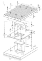
図5は、磁気デバイス1’の分解斜視図である。図6は、磁気デバイス1’の基板3’の各層の平面図である。図7は、磁気デバイス1’の断面図であって、図6のY−Y断面を示している。
FIG. 5 is an exploded perspective view of the
図5に示すように、基板3’の裏面をヒートシンク10の上面(フィン10fと反対側)と対向させ、かつ、基板3’の表面をヒートシンク10’の下面(フィン10f’と反対側)と対向させる。そして、各ねじ11’を、ヒートシンク10’に設けられた各貫通孔10a’と、スペーサである各スリーブ13と、基板3’に設けられた各貫通孔3aとに貫通させて、ヒートシンク10の各ねじ孔10aに螺合する。
As shown in FIG. 5, the back surface of the
これにより、図7に示すように、基板3’の表側外面層L2’側にヒートシンク10’が近接状態で固定され、裏側外面層L1’側にヒートシンク10が近接状態で固定される。上コア2aは、ヒートシンク10’の下側に設けられた凹部10k’に嵌め込まれる。基板3’とヒートシンク10、10’の間には、伝熱性を有する絶縁シート12、12’が挟み込まれる。ヒートシンク10は、本発明の「第1放熱器」の一例であり、ヒートシンク10’は、本発明の「第2放熱器」の一例である。
Accordingly, as shown in FIG. 7, the heat sink 10 'is fixed in the proximity state on the front side outer surface layer L2' side of the substrate 3 ', and the
前述の基板3と同様に、基板3’には、図6に示すように、スルーホール8i、8o、9a、9b、リード端子6i、6o、およびパッド8bが設けられている。また、基板3’の各層L1’、L2’には、コイルパターン4a〜4c、放熱部4s、4t、および放熱パターン5L1〜5L7、5r1〜5r7が設けられている。
Similar to the
また、基板3’には、複数の大径のスルーホール8dが設けられている。各スルーホール8dには、放熱ピン7a〜7fがそれぞれ埋め込まれている。放熱ピン7a〜7fは、銅などの導体から成る。各層L1’、L2’の放熱ピン7a〜7fの周囲には、銅箔から成るパッド8cが設けられている。放熱ピン7a〜7fやパッド8cの表面には、銅めっきが施されている。放熱ピン7a〜7fの上下端は、絶縁シート12、12’と接触している(図7参照)。
The substrate 3 'is provided with a plurality of large-diameter through
図6(a)に示すように、裏側外面層L1’において、コイルパターン4aの各放熱部4sには、パッド8cを介して放熱ピン7a、7c、7eがそれぞれ接続されている。また、コイルパターン4bの各放熱部4tには、パッド8cを介して放熱ピン7b、7d、7fがそれぞれ接続されている。放熱ピン7a〜7fおよびパッド8cは、周囲の放熱パターン5L1〜5L4、5r1〜5r4に対して絶縁されている。
As shown to Fig.6 (a), in back side outer surface layer L1 ', the thermal radiation pins 7a, 7c, and 7e are each connected to each
図6(b)に示すように、表側外面層L2’において、左側の放熱パターン5L5、5L6、5L7に対して、放熱ピン7c、7e、7aとこれらの周囲のパッド8cがそれぞれ接続されている。また、右側の放熱パターン5r5、5r6、5r7に対して、放熱ピン7d、7f、7bとこれらの周囲のパッド8cが接続されている。
As shown in FIG. 6B, in the front outer layer L2 ′, the heat radiation pins 7c, 7e, 7a and the
つまり、放熱ピン7c、7e、7aにより、裏側外面層L1’のコイルパターン4aと、表側外面層L2’の放熱パターン5L5、5L6、5L7が接続されている。また、放熱ピン7d、7f、7bにより、裏側外面層L1’のコイルパターン4bと、表側外面層L2’の放熱パターン5r5、5r6、5r7が接続されている。放熱ピン7a〜7fは、本発明の「放熱用接続部」の一例である。
That is, the
表側外面層L2’において、放熱パターン5L5〜5L7、5r5〜5r7と、コイルパターン4cとは別体になっていて、絶縁されている。
In the front side outer surface layer L2 ′, the heat radiation patterns 5L 5 to 5L 7 , 5r 5 to 5r 7 and the
コイルパターン4a〜4cに大電流が流れたとき、表側外面層L2’では、コイルパターン4cで発生した熱が、該コイルパターン4cの表面から絶縁シート12’を介してヒートシンク10’に伝わり、ヒートシンク10’で放熱される。また、基板3’の熱が、放熱パターン5L5〜5L7、5r5〜5r7の表面から絶縁シート12’を介してヒートシンク10’に伝わり、ヒートシンク10’で放熱される。
When a large current flows through the
裏側外面層L1’では、コイルパターン4a、4bで発生した熱が、放熱部4s、4tに拡散されて、コイルパターン4a、4bと放熱部4s、4tの表面から絶縁シート12を介してヒートシンク10に伝わり、ヒートシンク10で放熱される。また、コイルパターン4a、4bで発生した熱が、放熱部4s、4tから放熱ピン7a〜7fを介して表側外面層L2’の放熱パターン5L5〜5L7、5r5〜5r7に伝わって、該放熱パターン5L5〜5L7、5r5〜5r7に拡散される。そして、その熱が、放熱パターン5L5〜5L7、5r5〜5r7の表面から絶縁シート12を介してヒートシンク10に伝わり、ヒートシンク10で放熱される。
In the backside outer surface layer L1 ′, heat generated in the
また、裏側外面層L1’では、基板3’の熱が、放熱パターン5L1〜5L4、5r1〜5r4の表面から絶縁シート12を介してヒートシンク10に伝わり、ヒートシンク10で放熱される。
Further, in the backside outer surface layer L1 ′, the heat of the
上記第2実施形態によると、基板3’の裏側外面層L1’側と表側外面層L2’側に、それぞれヒートシンク10、10’が設けられている。このため、裏側外面層L1’側だけでなく、表側外面層L2’においても、コイルパターン4cで発生した熱を、ヒートシンク10’により放熱させ易くすることができる。
According to the second embodiment, the heat sinks 10 and 10 'are provided on the back side outer surface layer L1' side and the front side outer surface layer L2 'side of the substrate 3', respectively. For this reason, the heat generated in the
また、裏側外面層L1’のコイルパターン4a、4bで発生した熱は、ヒートシンク10で放熱されるだけでなく、放熱ピン7a〜7fと表側外面層L2’の放熱パターン5L5〜5L7、5r5〜5r7などを介してヒートシンク10’に伝わり、ヒートシンク10’でも放熱される。このため、コイルパターン4cよりも発熱量の多いコイルパターン4a、4bの熱を、両方のヒートシンク10、10’により効率良く放熱させることができる。
Further, the heat generated in the
よって、複数の層L1’、L2’に幅の異なるコイルパターン4a〜4cが設けられた基板3’において、コイルパターン4a〜4cにより大きな電流が流れても、基板3’の放熱性能を一層高めることができる。また、コイルパターン4a〜4cの発熱を許容することができる。
Therefore, even when a large current flows through the
本発明では、以上述べた以外にも種々の実施形態を採用することができる。たとえば、以上の実施形態では、基板3、3’の表裏両面に設けた各外面層L1、L2、L1’、L2’にコイルパターン4a〜4cを形成した例を示したが、本発明はこれのみに限定するものではない。これ以外に、3層以上を有する多層基板において、一方の外面層を含んだ、2層以上にコイルパターンを形成してもよい。
In the present invention, various embodiments other than those described above can be adopted. For example, in the above embodiment, the
また、以上の実施形態では、コア2aの3つの凸部2m、2L、2rに巻回するように、基板3、3’にコイルパターン4a〜4cを形成した例を示したが、本発明はこれのみに限定するものではない。コイルパターンは、コアの少なくとも1つの凸部に巻回されていればよい。
Moreover, although the above embodiment showed the example which formed the
また、以上の実施形態では、図4や図7に示したように、コイルパターン4a〜4cの厚みがほぼ同等になっている例を示したが、本発明はこれのみに限定するものではなく、コイルパターン4a〜4cの厚みは異なっていてもよい。また、コイルパターン4a〜4cの幅が異なる部分の断面積をほぼ同等にしてもよい。
Moreover, in the above embodiment, as shown in FIG.4 and FIG.7, although the example where the thickness of
また、図6および図7に示したように、第2実施形態では、裏側外面層L1’のコイルパターン4a、4bと、表側外面層L2’の放熱パターン5L7〜5L9、5r7〜5r9を、スルーホール8dに埋設した放熱ピン7a〜7fにより接続した例を示したが、本発明はこれのみに限定するものではない。これ以外に、たとえば端子、ピン、およびスルーホールなどの少なくとも1つの接続手段により、異なる層のコイルパターンと放熱パターンを接続してもよい。
As shown in FIGS. 6 and 7, in the second embodiment, the
また、以上の実施形態では、基板3の裏側外面層L1、L1’にあるコイルパターン4a、4bを拡張して、放熱部4s、4tを設けた例を示したが、本発明はこれのみに限定するものではない。表側外面層L2、L2’にあるコイルパターン4cも拡張して、放熱部を設けてもよい。また、コイルパターン4cに対応する放熱パターンを裏側外面層L1、L1’に設けて、該放熱パターンとコイルパターン4cとを放熱ピンなどの接続手段により接続してもよい。
Moreover, in the above embodiment, although the
また、以上の実施形態では、放熱器として、ヒートシンク10、10’を用いた例を示したが、本発明はこれのみに限定するものではなく、これ以外の、空冷式や水冷式の放熱器、または冷媒を用いた放熱器などを用いてもよい。また、金属製の放熱器だけでなく、たとえば、熱伝導性の高い樹脂で形成された放熱器を用いてもよい。この場合、放熱器と基板との間に絶縁シート12、12’を設ける必要はなく、絶縁シート12、12’を省略することができる。
Moreover, although the example using
また、以上の実施形態では、厚銅箔基板を用いた例を示したが、本発明はこれのみに限定するものではなく、一般的な樹脂製のプリント基板や金属製の基板などのような、他の基板を用いてもよい。金属製の基板の場合は、基材とコイルパターンとの間に絶縁体を設ければよい。 Moreover, although the example using a thick copper foil board | substrate was shown in the above embodiment, this invention is not limited only to this, A general resin-made printed boards, metal boards, etc. Other substrates may be used. In the case of a metal substrate, an insulator may be provided between the base material and the coil pattern.
また、以上の実施形態では、E字形の上コア2aにI字形の下コア2bを組み合わせた例を示したが、本発明は、2つのE字形コアを組み合わせた磁気デバイスにも適用することができる。
Moreover, although the example which combined the I-shaped
さらに、以上の実施形態では、車両用のスイッチング電源装置100における、平滑回路55のチョークコイルLとして使用される磁気デバイス1、1’に本発明を適用した例を挙げたが、トランス53(図1)として使用される磁気デバイスに対しても、本発明を適用することは可能である。また、車両以外の、たとえば電子機器用のスイッチング電源装置で使用される磁気デバイスにも本発明を適用することは可能である。
Furthermore, in the above embodiment, the example in which the present invention is applied to the
1、1’ 磁気デバイス
2a 上コア
2b 下コア
3、3’ 基板
4a、4b、4c コイルパターン
4s、4t 放熱部
5L7、5L8、5L9、5r7、5r8、5r9 放熱パターン
7a、7b、7c、7d、7e、7f 放熱ピン
10、10’ ヒートシンク
L1、L1’ 裏側外面層
L2、L2’ 表側外面層
W1、W2 コイルパターンの幅
1,1 '
Claims (6)
絶縁体から成り、前記コアが貫通する基板と、
前記基板の所定の層に設けられた、導体から成るコイルパターンと、を備えた磁気デバイスにおいて、
前記基板の一方の外面層にある前記コイルパターンの幅は、他の層にある前記コイルパターンの幅より細く、
前記一方の外面層側に放熱器を設けた、ことを特徴とする磁気デバイス。 A core made of magnetic material,
A substrate made of an insulator through which the core penetrates;
In a magnetic device provided with a coil pattern made of a conductor provided in a predetermined layer of the substrate,
The width of the coil pattern on one outer surface layer of the substrate is narrower than the width of the coil pattern on the other layer,
A magnetic device comprising a radiator on the one outer surface layer side.
前記基板の一方の外面層にある前記コイルパターンの巻き数は、他の層にある前記コイルパターンの巻き数より多い、ことを特徴とする磁気デバイス。 The magnetic device according to claim 1.
The magnetic device according to claim 1, wherein the number of turns of the coil pattern on one outer surface layer of the substrate is greater than the number of turns of the coil pattern on the other layer.
前記一方の外面層にある前記コイルパターンを部分的に拡張することにより、当該一方の外面層に、導体から成る放熱部を設けた、ことを特徴とする磁気デバイス。 The magnetic device according to claim 1 or 2,
A magnetic device, wherein a heat radiating portion made of a conductor is provided on the one outer surface layer by partially expanding the coil pattern on the one outer surface layer.
前記基板は、表面と裏面にそれぞれ外面層が設けられ、
前記コイルパターンは、前記基板の前記一方の外面層と前記他方の外面層にそれぞれ設けられている、ことを特徴とする磁気デバイス。 The magnetic device according to any one of claims 1 to 3,
The substrate is provided with an outer surface layer on each of the front surface and the back surface,
2. The magnetic device according to claim 1, wherein the coil pattern is provided on each of the one outer surface layer and the other outer surface layer of the substrate.
前記一方の外面層側に設けた放熱器が第1放熱器であり、
前記他方の外面層側に第2放熱器をさらに設けた、ことを特徴とする磁気デバイス。 The magnetic device according to claim 4.
The radiator provided on the one outer surface layer side is a first radiator,
2. A magnetic device, wherein a second heat radiator is further provided on the other outer surface layer side.
前記他方の外面層にある前記コイルパターンと別体で、前記他方の外面層に設けられた導体から成る放熱パターンと、
前記基板に設けられた導体から成り、前記一方の外面層にある前記コイルパターンと前記他方の外面層にある前記放熱パターンとを接続する放熱用接続部と、をさらに備えた、ことを特徴とする磁気デバイス。 The magnetic device according to claim 5, wherein
A heat dissipating pattern consisting of a conductor provided on the other outer surface layer separately from the coil pattern on the other outer surface layer;
A heat dissipating connecting portion for connecting the coil pattern on the one outer surface layer and the heat dissipating pattern on the other outer surface layer, further comprising a conductor provided on the substrate, Magnetic device to be used.
Priority Applications (1)
| Application Number | Priority Date | Filing Date | Title |
|---|---|---|---|
| JP2013069812A JP6153158B2 (en) | 2013-03-28 | 2013-03-28 | Magnetic device |
Applications Claiming Priority (1)
| Application Number | Priority Date | Filing Date | Title |
|---|---|---|---|
| JP2013069812A JP6153158B2 (en) | 2013-03-28 | 2013-03-28 | Magnetic device |
Publications (2)
| Publication Number | Publication Date |
|---|---|
| JP2014192517A true JP2014192517A (en) | 2014-10-06 |
| JP6153158B2 JP6153158B2 (en) | 2017-06-28 |
Family
ID=51838469
Family Applications (1)
| Application Number | Title | Priority Date | Filing Date |
|---|---|---|---|
| JP2013069812A Active JP6153158B2 (en) | 2013-03-28 | 2013-03-28 | Magnetic device |
Country Status (1)
| Country | Link |
|---|---|
| JP (1) | JP6153158B2 (en) |
Cited By (4)
| Publication number | Priority date | Publication date | Assignee | Title |
|---|---|---|---|---|
| JP6234615B1 (en) * | 2016-05-31 | 2017-11-22 | 新電元工業株式会社 | Magnetic parts |
| US10748700B2 (en) | 2016-05-31 | 2020-08-18 | Shindengen Electric Manufacturing Co., Ltd. | Coil structure and magnetic component |
| US10916367B2 (en) | 2016-01-21 | 2021-02-09 | Mitsubishi Electric Corporation | Circuit device and power conversion device |
| US11239021B2 (en) | 2016-06-24 | 2022-02-01 | Mitsubishi Electric Corporation | Isolated converter |
Citations (6)
| Publication number | Priority date | Publication date | Assignee | Title |
|---|---|---|---|---|
| JPS5931210U (en) * | 1982-08-19 | 1984-02-27 | 松下電器産業株式会社 | Power transformer heat dissipation device |
| JPH0420217U (en) * | 1990-06-11 | 1992-02-20 | ||
| JPH0786755A (en) * | 1993-09-17 | 1995-03-31 | Nagano Japan Radio Co | Printed board |
| JP2007059839A (en) * | 2005-08-26 | 2007-03-08 | Matsushita Electric Works Ltd | Lc composite component |
| JP2012156461A (en) * | 2011-01-28 | 2012-08-16 | Toyota Industries Corp | Electronic apparatus |
| US20120287582A1 (en) * | 2011-05-11 | 2012-11-15 | Patrizio Vinciarelli | Panel-Molded Electronic Assemblies |
-
2013
- 2013-03-28 JP JP2013069812A patent/JP6153158B2/en active Active
Patent Citations (6)
| Publication number | Priority date | Publication date | Assignee | Title |
|---|---|---|---|---|
| JPS5931210U (en) * | 1982-08-19 | 1984-02-27 | 松下電器産業株式会社 | Power transformer heat dissipation device |
| JPH0420217U (en) * | 1990-06-11 | 1992-02-20 | ||
| JPH0786755A (en) * | 1993-09-17 | 1995-03-31 | Nagano Japan Radio Co | Printed board |
| JP2007059839A (en) * | 2005-08-26 | 2007-03-08 | Matsushita Electric Works Ltd | Lc composite component |
| JP2012156461A (en) * | 2011-01-28 | 2012-08-16 | Toyota Industries Corp | Electronic apparatus |
| US20120287582A1 (en) * | 2011-05-11 | 2012-11-15 | Patrizio Vinciarelli | Panel-Molded Electronic Assemblies |
Cited By (8)
| Publication number | Priority date | Publication date | Assignee | Title |
|---|---|---|---|---|
| US10916367B2 (en) | 2016-01-21 | 2021-02-09 | Mitsubishi Electric Corporation | Circuit device and power conversion device |
| JP6234615B1 (en) * | 2016-05-31 | 2017-11-22 | 新電元工業株式会社 | Magnetic parts |
| WO2017208333A1 (en) * | 2016-05-31 | 2017-12-07 | 新電元工業株式会社 | Magnetic component |
| CN107667408A (en) * | 2016-05-31 | 2018-02-06 | 新电元工业株式会社 | Magnetic part |
| CN107667408B (en) * | 2016-05-31 | 2019-07-05 | 新电元工业株式会社 | Magnetic part |
| US10410784B2 (en) | 2016-05-31 | 2019-09-10 | Shindengen Electric Manufacturing Co., Ltd. | Magnetic component |
| US10748700B2 (en) | 2016-05-31 | 2020-08-18 | Shindengen Electric Manufacturing Co., Ltd. | Coil structure and magnetic component |
| US11239021B2 (en) | 2016-06-24 | 2022-02-01 | Mitsubishi Electric Corporation | Isolated converter |
Also Published As
| Publication number | Publication date |
|---|---|
| JP6153158B2 (en) | 2017-06-28 |
Similar Documents
| Publication | Publication Date | Title |
|---|---|---|
| JP6084147B2 (en) | Coil integrated printed circuit board, magnetic device | |
| JP6084079B2 (en) | Magnetic device | |
| US8686823B2 (en) | Electronic unit | |
| JP6084148B2 (en) | Coil integrated printed circuit board, magnetic device | |
| JP2011077328A (en) | Transformer and switching power supply device | |
| JP6213979B2 (en) | Magnetic device | |
| JP6168556B2 (en) | Coil integrated printed circuit board, magnetic device | |
| JP6153158B2 (en) | Magnetic device | |
| JP6120623B2 (en) | Magnetic device | |
| JP2017199940A (en) | Magnetic device | |
| JP2015095938A (en) | Power supply device | |
| JP6084103B2 (en) | Magnetic device | |
| JP6261032B2 (en) | Multilayer printed circuit boards, magnetic devices | |
| JP6261071B2 (en) | Coil integrated printed circuit board, magnetic device | |
| WO2014141668A1 (en) | Magnetic device | |
| JP2014170869A (en) | Magnetic device | |
| JP2014179402A (en) | Magnetic device | |
| JP2014160785A (en) | Magnetic device | |
| JP2015088689A (en) | Multilayer printed board and magnetic device | |
| JP6120619B2 (en) | Magnetic device | |
| JP3022180B2 (en) | Mounting structure of printed coil type transformer | |
| JP2014179399A (en) | Magnetic device | |
| JP2014179403A (en) | Mounting structure of electronic component |
Legal Events
| Date | Code | Title | Description |
|---|---|---|---|
| A621 | Written request for application examination |
Free format text: JAPANESE INTERMEDIATE CODE: A621 Effective date: 20151214 |
|
| A977 | Report on retrieval |
Free format text: JAPANESE INTERMEDIATE CODE: A971007 Effective date: 20161018 |
|
| A131 | Notification of reasons for refusal |
Free format text: JAPANESE INTERMEDIATE CODE: A131 Effective date: 20161122 |
|
| A521 | Request for written amendment filed |
Free format text: JAPANESE INTERMEDIATE CODE: A523 Effective date: 20170117 |
|
| TRDD | Decision of grant or rejection written | ||
| A01 | Written decision to grant a patent or to grant a registration (utility model) |
Free format text: JAPANESE INTERMEDIATE CODE: A01 Effective date: 20170524 |
|
| A61 | First payment of annual fees (during grant procedure) |
Free format text: JAPANESE INTERMEDIATE CODE: A61 Effective date: 20170524 |
|
| R150 | Certificate of patent or registration of utility model |
Ref document number: 6153158 Country of ref document: JP Free format text: JAPANESE INTERMEDIATE CODE: R150 |
|
| S111 | Request for change of ownership or part of ownership |
Free format text: JAPANESE INTERMEDIATE CODE: R313113 |
|
| R350 | Written notification of registration of transfer |
Free format text: JAPANESE INTERMEDIATE CODE: R350 |
|
| R250 | Receipt of annual fees |
Free format text: JAPANESE INTERMEDIATE CODE: R250 |
|
| R250 | Receipt of annual fees |
Free format text: JAPANESE INTERMEDIATE CODE: R250 |
|
| R250 | Receipt of annual fees |
Free format text: JAPANESE INTERMEDIATE CODE: R250 |
|
| R250 | Receipt of annual fees |
Free format text: JAPANESE INTERMEDIATE CODE: R250 |