JP2014179318A - Led light bulb with structural support - Google Patents
Led light bulb with structural support Download PDFInfo
- Publication number
- JP2014179318A JP2014179318A JP2014037120A JP2014037120A JP2014179318A JP 2014179318 A JP2014179318 A JP 2014179318A JP 2014037120 A JP2014037120 A JP 2014037120A JP 2014037120 A JP2014037120 A JP 2014037120A JP 2014179318 A JP2014179318 A JP 2014179318A
- Authority
- JP
- Japan
- Prior art keywords
- led
- support structure
- bulb
- light
- coating
- Prior art date
- Legal status (The legal status is an assumption and is not a legal conclusion. Google has not performed a legal analysis and makes no representation as to the accuracy of the status listed.)
- Pending
Links
Images


Classifications
-
- F—MECHANICAL ENGINEERING; LIGHTING; HEATING; WEAPONS; BLASTING
- F21—LIGHTING
- F21V—FUNCTIONAL FEATURES OR DETAILS OF LIGHTING DEVICES OR SYSTEMS THEREOF; STRUCTURAL COMBINATIONS OF LIGHTING DEVICES WITH OTHER ARTICLES, NOT OTHERWISE PROVIDED FOR
- F21V29/00—Protecting lighting devices from thermal damage; Cooling or heating arrangements specially adapted for lighting devices or systems
- F21V29/50—Cooling arrangements
- F21V29/70—Cooling arrangements characterised by passive heat-dissipating elements, e.g. heat-sinks
- F21V29/83—Cooling arrangements characterised by passive heat-dissipating elements, e.g. heat-sinks the elements having apertures, ducts or channels, e.g. heat radiation holes
-
- F—MECHANICAL ENGINEERING; LIGHTING; HEATING; WEAPONS; BLASTING
- F21—LIGHTING
- F21V—FUNCTIONAL FEATURES OR DETAILS OF LIGHTING DEVICES OR SYSTEMS THEREOF; STRUCTURAL COMBINATIONS OF LIGHTING DEVICES WITH OTHER ARTICLES, NOT OTHERWISE PROVIDED FOR
- F21V21/00—Supporting, suspending, or attaching arrangements for lighting devices; Hand grips
-
- F—MECHANICAL ENGINEERING; LIGHTING; HEATING; WEAPONS; BLASTING
- F21—LIGHTING
- F21K—NON-ELECTRIC LIGHT SOURCES USING LUMINESCENCE; LIGHT SOURCES USING ELECTROCHEMILUMINESCENCE; LIGHT SOURCES USING CHARGES OF COMBUSTIBLE MATERIAL; LIGHT SOURCES USING SEMICONDUCTOR DEVICES AS LIGHT-GENERATING ELEMENTS; LIGHT SOURCES NOT OTHERWISE PROVIDED FOR
- F21K9/00—Light sources using semiconductor devices as light-generating elements, e.g. using light-emitting diodes [LED] or lasers
- F21K9/20—Light sources comprising attachment means
- F21K9/23—Retrofit light sources for lighting devices with a single fitting for each light source, e.g. for substitution of incandescent lamps with bayonet or threaded fittings
- F21K9/232—Retrofit light sources for lighting devices with a single fitting for each light source, e.g. for substitution of incandescent lamps with bayonet or threaded fittings specially adapted for generating an essentially omnidirectional light distribution, e.g. with a glass bulb
-
- F—MECHANICAL ENGINEERING; LIGHTING; HEATING; WEAPONS; BLASTING
- F21—LIGHTING
- F21K—NON-ELECTRIC LIGHT SOURCES USING LUMINESCENCE; LIGHT SOURCES USING ELECTROCHEMILUMINESCENCE; LIGHT SOURCES USING CHARGES OF COMBUSTIBLE MATERIAL; LIGHT SOURCES USING SEMICONDUCTOR DEVICES AS LIGHT-GENERATING ELEMENTS; LIGHT SOURCES NOT OTHERWISE PROVIDED FOR
- F21K9/00—Light sources using semiconductor devices as light-generating elements, e.g. using light-emitting diodes [LED] or lasers
- F21K9/90—Methods of manufacture
-
- F—MECHANICAL ENGINEERING; LIGHTING; HEATING; WEAPONS; BLASTING
- F21—LIGHTING
- F21V—FUNCTIONAL FEATURES OR DETAILS OF LIGHTING DEVICES OR SYSTEMS THEREOF; STRUCTURAL COMBINATIONS OF LIGHTING DEVICES WITH OTHER ARTICLES, NOT OTHERWISE PROVIDED FOR
- F21V19/00—Fastening of light sources or lamp holders
- F21V19/001—Fastening of light sources or lamp holders the light sources being semiconductors devices, e.g. LEDs
-
- F—MECHANICAL ENGINEERING; LIGHTING; HEATING; WEAPONS; BLASTING
- F21—LIGHTING
- F21V—FUNCTIONAL FEATURES OR DETAILS OF LIGHTING DEVICES OR SYSTEMS THEREOF; STRUCTURAL COMBINATIONS OF LIGHTING DEVICES WITH OTHER ARTICLES, NOT OTHERWISE PROVIDED FOR
- F21V7/00—Reflectors for light sources
- F21V7/0066—Reflectors for light sources specially adapted to cooperate with point like light sources; specially adapted to cooperate with light sources the shape of which is unspecified
-
- F—MECHANICAL ENGINEERING; LIGHTING; HEATING; WEAPONS; BLASTING
- F21—LIGHTING
- F21Y—INDEXING SCHEME ASSOCIATED WITH SUBCLASSES F21K, F21L, F21S and F21V, RELATING TO THE FORM OR THE KIND OF THE LIGHT SOURCES OR OF THE COLOUR OF THE LIGHT EMITTED
- F21Y2107/00—Light sources with three-dimensionally disposed light-generating elements
-
- F—MECHANICAL ENGINEERING; LIGHTING; HEATING; WEAPONS; BLASTING
- F21—LIGHTING
- F21Y—INDEXING SCHEME ASSOCIATED WITH SUBCLASSES F21K, F21L, F21S and F21V, RELATING TO THE FORM OR THE KIND OF THE LIGHT SOURCES OR OF THE COLOUR OF THE LIGHT EMITTED
- F21Y2115/00—Light-generating elements of semiconductor light sources
- F21Y2115/10—Light-emitting diodes [LED]
-
- H—ELECTRICITY
- H05—ELECTRIC TECHNIQUES NOT OTHERWISE PROVIDED FOR
- H05K—PRINTED CIRCUITS; CASINGS OR CONSTRUCTIONAL DETAILS OF ELECTRIC APPARATUS; MANUFACTURE OF ASSEMBLAGES OF ELECTRICAL COMPONENTS
- H05K1/00—Printed circuits
- H05K1/18—Printed circuits structurally associated with non-printed electric components
- H05K1/189—Printed circuits structurally associated with non-printed electric components characterised by the use of a flexible or folded printed circuit
-
- H—ELECTRICITY
- H05—ELECTRIC TECHNIQUES NOT OTHERWISE PROVIDED FOR
- H05K—PRINTED CIRCUITS; CASINGS OR CONSTRUCTIONAL DETAILS OF ELECTRIC APPARATUS; MANUFACTURE OF ASSEMBLAGES OF ELECTRICAL COMPONENTS
- H05K2201/00—Indexing scheme relating to printed circuits covered by H05K1/00
- H05K2201/05—Flexible printed circuits [FPCs]
- H05K2201/056—Folded around rigid support or component
-
- H—ELECTRICITY
- H05—ELECTRIC TECHNIQUES NOT OTHERWISE PROVIDED FOR
- H05K—PRINTED CIRCUITS; CASINGS OR CONSTRUCTIONAL DETAILS OF ELECTRIC APPARATUS; MANUFACTURE OF ASSEMBLAGES OF ELECTRICAL COMPONENTS
- H05K2201/00—Indexing scheme relating to printed circuits covered by H05K1/00
- H05K2201/10—Details of components or other objects attached to or integrated in a printed circuit board
- H05K2201/10007—Types of components
- H05K2201/10106—Light emitting diode [LED]
-
- H—ELECTRICITY
- H05—ELECTRIC TECHNIQUES NOT OTHERWISE PROVIDED FOR
- H05K—PRINTED CIRCUITS; CASINGS OR CONSTRUCTIONAL DETAILS OF ELECTRIC APPARATUS; MANUFACTURE OF ASSEMBLAGES OF ELECTRICAL COMPONENTS
- H05K3/00—Apparatus or processes for manufacturing printed circuits
- H05K3/0058—Laminating printed circuit boards onto other substrates, e.g. metallic substrates
-
- Y—GENERAL TAGGING OF NEW TECHNOLOGICAL DEVELOPMENTS; GENERAL TAGGING OF CROSS-SECTIONAL TECHNOLOGIES SPANNING OVER SEVERAL SECTIONS OF THE IPC; TECHNICAL SUBJECTS COVERED BY FORMER USPC CROSS-REFERENCE ART COLLECTIONS [XRACs] AND DIGESTS
- Y10—TECHNICAL SUBJECTS COVERED BY FORMER USPC
- Y10T—TECHNICAL SUBJECTS COVERED BY FORMER US CLASSIFICATION
- Y10T29/00—Metal working
- Y10T29/49—Method of mechanical manufacture
- Y10T29/49002—Electrical device making
- Y10T29/49117—Conductor or circuit manufacturing
- Y10T29/49124—On flat or curved insulated base, e.g., printed circuit, etc.
- Y10T29/4913—Assembling to base an electrical component, e.g., capacitor, etc.
Landscapes
- Engineering & Computer Science (AREA)
- General Engineering & Computer Science (AREA)
- Physics & Mathematics (AREA)
- Microelectronics & Electronic Packaging (AREA)
- Optics & Photonics (AREA)
- Manufacturing & Machinery (AREA)
- Non-Portable Lighting Devices Or Systems Thereof (AREA)
- Arrangement Of Elements, Cooling, Sealing, Or The Like Of Lighting Devices (AREA)
- Fastening Of Light Sources Or Lamp Holders (AREA)
- Led Device Packages (AREA)
Abstract
Description
本出願は一般に発光ダイオード(LED)電球に関する。本出願はまた、このようなLED電球に関連する構成要素、デバイス、およびシステムに関する。 This application relates generally to light emitting diode (LED) bulbs. The present application also relates to components, devices, and systems associated with such LED bulbs.
いくつか実施形態は発光ダイオード(LED)電球を含む。LED電球は口金と、該口金に連結されるとともに発光面と開放容積(open volume)のための外形を画定する形状に形成される少なくとも一の支持構造と、を含む。LED電球は二以上の電気的に接続されるLEDを含む少なくとも一のLEDアセンブリを含む。LEDアセンブリは、支持構造の長さに沿って支持構造に取り付けられるとともに該支持構造に物理的接触することにて発光面を形成する。支持構造はLEDアセンブリの互いに隣接しているセグメント間に開口を有している。 Some embodiments include a light emitting diode (LED) bulb. The LED bulb includes a base and at least one support structure connected to the base and formed in a shape that defines a light emitting surface and an outer shape for an open volume. The LED bulb includes at least one LED assembly that includes two or more electrically connected LEDs. The LED assembly is attached to the support structure along the length of the support structure and forms a light emitting surface by being in physical contact with the support structure. The support structure has an opening between adjacent segments of the LED assembly.
いくつかのインプリメンテーションによれば、発光面によって画定される容積は、約0.7より大なる球度を有する。いくつかのインプリメンテーションにおいて、LED電球の表面積当たりの光出力は、LED電球の外部表面積の1cm2(平方センチメートル)当たりで、好ましくは、約0.3〜30ルーメン、より好ましくは、約0.5〜20ルーメンである。 According to some implementations, the volume defined by the light emitting surface has a sphericity greater than about 0.7. In some implementations, the light output per surface area of the LED bulb is preferably about 0.3 to 30 lumens, more preferably about 0.00, per 1 cm 2 (square centimeters) of the external surface area of the LED bulb. 5-20 lumens.
例えば、LED電球の寸法は同等の明るさの白熱電球に類似している。LED電球は、螺線形、円筒形、円錐形などの任意の形状を有することができる。いくつかの構成において、LED電球は、多数の長尺の支持エレメントと多数のLEDアセンブリとを含むことができ、その際、該多数のLEDアセンブリの各々は複数の長尺の支持エレメントの各々に取り付けられる。或いは、LEDアセンブリは、単一の長尺の支持エレメントを含むことができ、該単一の長尺の支持エレメントは単一のLEDアセンブリまたは多数のLEDアセンブリに連結される。 For example, the dimensions of LED bulbs are similar to incandescent bulbs of similar brightness. The LED bulb can have any shape such as spiral, cylindrical, conical. In some configurations, the LED bulb may include multiple elongated support elements and multiple LED assemblies, each of the multiple LED assemblies being attached to each of the multiple elongated support elements. It is attached. Alternatively, the LED assembly can include a single elongate support element that is coupled to a single LED assembly or multiple LED assemblies.
支持構造は、金属を含むことができ、金属は、陽極酸化および/または酸化されおよび/または或いは他の方法で塗膜されてよい。支持構造は、プラスチック、例えば、成形プラスチックを含むことができる。いくつかのインプリメンテーションにおいて、支持構造はいくつかの材料の複合体を含む。支持構造は約100W/mKを上回る熱伝導率を有する材料を含むことができる。LEDから発生した熱を消散するように構成されている冷却フィンは、必要に応じて、支持構造に設けられる。様々なインプリメンテーションにおいて、冷却フィンは、開放容積の外側および/または内側に配向される。いくつかの構成によれば、支持構造の少なくとも一の主要表面は同じ大きさのテクスチャ(粗度)処理されていない表面より表面積が少なくとも3倍も大きい表面テクスチャを有している。支持構造は光散乱面を有することができる、いくつかの構成によれば、支持構造は、約320〜700nm(ナノメートル)の波長に対して約85%より高い反射率を有している。いくつかの実施形態において、支持構造は硬化された構造的塗膜を含むことができる。 The support structure can include a metal, which can be anodized and / or oxidized and / or coated in other ways. The support structure can include plastic, eg, molded plastic. In some implementations, the support structure includes a composite of several materials. The support structure can include a material having a thermal conductivity greater than about 100 W / mK. Cooling fins configured to dissipate heat generated from the LEDs are provided in the support structure as needed. In various implementations, the cooling fins are oriented outside and / or inside the open volume. According to some configurations, at least one major surface of the support structure has a surface texture that has a surface area that is at least three times greater than an untextured surface of the same size. The support structure can have a light scattering surface. According to some configurations, the support structure has a reflectivity greater than about 85% for wavelengths between about 320 and 700 nm (nanometers). In some embodiments, the support structure can include a cured structural coating.
いくつかの構成において、LEDアセンブリは可撓性基板の長さに沿って単列で配列される複数のLEDを含む。或いは、LEDアセンブリは可撓性基板の長さに沿って二以上の列で配列された複数のLEDを含むことができる。LEDは電気的に接続され、例えば、可撓性基板内またはその上に配置されたLED同士の間で電気的接続によって、例えば、並列に電気的接続され得る。可撓性基板は第1の主要表面とこれに対向する第2の主要表面を有しており、LEDの各々は可撓性基板の主要表面にほぼ垂直を成す発光面またはエッジを有している。 In some configurations, the LED assembly includes a plurality of LEDs arranged in a single row along the length of the flexible substrate. Alternatively, the LED assembly can include a plurality of LEDs arranged in two or more rows along the length of the flexible substrate. The LEDs are electrically connected, for example, can be electrically connected, for example in parallel, by electrical connection between LEDs disposed in or on the flexible substrate. The flexible substrate has a first major surface and a second major surface opposite thereto, and each of the LEDs has a light emitting surface or edge that is substantially perpendicular to the major surface of the flexible substrate. Yes.
いくつかのインプリメンテーションにおいて、LEDアセンブリは第1の主要表面とこれに対向する第2の主要表面を有する可撓性基板を含む。LEDの各々は可撓性基板の主要表面にほぼ平行を成す発光面またはエッジを有している。いくつかのインプリメンテーションにおいて、支持構造は第1の主要表面とこれに対向する第2の主要表面を有している。LEDアセンブリは長尺の支持構造の第1の主要表面上に配置される。或いは、第1のLEDアセンブリは長尺の支持体の第1の主要表面に沿って配置することができ、第2のLEDアセンブリは長尺支持体の第2の主要表面に沿って配置することができる。 In some implementations, the LED assembly includes a flexible substrate having a first major surface and an opposing second major surface. Each of the LEDs has a light emitting surface or edge that is substantially parallel to the major surface of the flexible substrate. In some implementations, the support structure has a first major surface and an opposing second major surface. The LED assembly is disposed on the first major surface of the elongated support structure. Alternatively, the first LED assembly can be disposed along the first major surface of the elongated support and the second LED assembly is disposed along the second major surface of the elongated support. Can do.
いくつかのインプリメンテーションにおいて、LEDアセンブリ基板は可撓性のプリント回路基板を含み、LEDは個別の表面実装LEDを含む。いくつかのインプリメンテーションにおいて、LEDは集積回路として共に形成されるマイクロLEDを含む。 In some implementations, the LED assembly substrate includes a flexible printed circuit board, and the LEDs include individual surface mount LEDs. In some implementations, the LEDs include micro LEDs that are formed together as an integrated circuit.
塗膜はLEDアセンブリの少なくとも一部を覆って配置され得る。塗膜はセラミック、ガラス、ポリマ、プラスチック、金属粉末の一以上を含み得る。いくつかの構成において、塗膜は、LEDから発せられた光を透過させおよび/または散乱させるように構成されている。塗膜はLEDから発せられた光を方向付けるように構成されているレンズとして作用することができる。いくつかの場合において、塗膜は周囲空気に露出される表面を有することができる。例えば、塗膜表面は同じ大きさのテクスチャ処理されていない表面より表面積が少なくとも3倍も大きい表面テクスチャを有することができる。LED電球は支持構造に配置された少なくとも一の熱拡散層または塗膜を含むことができる。 The coating can be disposed over at least a portion of the LED assembly. The coating can include one or more of ceramic, glass, polymer, plastic, metal powder. In some configurations, the coating is configured to transmit and / or scatter light emitted from the LED. The coating can act as a lens configured to direct the light emitted from the LED. In some cases, the coating can have a surface that is exposed to ambient air. For example, the coating surface can have a surface texture that is at least three times as large in surface area as an untextured surface of the same size. The LED bulb may include at least one heat diffusion layer or coating disposed on the support structure.
いくつかの態様によれば、光シートはLED上に配置することができる。いくつかの場合において、光シートはLEDから発せられた光を拡散するように構成することができる。いくつかの場合において、光シートは、光シートから光を透過する前に、光シートを通過する光路に沿ってLEDから発せられた光を導くように構成することができる。例えば、光シートはLEDアセンブリ上に配置されている塗膜に埋め込むことができる。 According to some aspects, the light sheet can be disposed on the LED. In some cases, the light sheet can be configured to diffuse the light emitted from the LED. In some cases, the light sheet can be configured to direct light emitted from the LEDs along a light path through the light sheet before transmitting light from the light sheet. For example, the light sheet can be embedded in a coating disposed on the LED assembly.
いくつかのインプリメンテーションにおいて、第1の群のLEDは電気的に連結されて比較的低い光出力を提供し、第2の群のLEDは電気的に連結されて比較的高い光出力を提供する。 In some implementations, the first group of LEDs are electrically coupled to provide a relatively low light output, and the second group of LEDs are electrically coupled to provide a relatively high light output. To do.
いくつかの実施形態はLED電球を作る方法に関する。支持構造は所定の形状に形成される。所定の形状は発光面と開放容積の外形を画定する。少なくとも一のLEDは支持構造に取り付けられる。LEDアセンブリは基板とこの基板に沿って互いに離間されている複数の電気的に接続されたLEDとを含む。 Some embodiments relate to a method of making an LED bulb. The support structure is formed in a predetermined shape. The predetermined shape defines a light emitting surface and an open volume outline. At least one LED is attached to the support structure. The LED assembly includes a substrate and a plurality of electrically connected LEDs spaced apart from each other along the substrate.
いくつかの場合において、支持構造は、少なくとも一のLEDアセンブリを取り付ける前に、所定の形状に形成される。或いは、LEDアセンブリは、支持構造が所定の形状に形成される前に、取り付けることができる。支持構造を所定の形状に形成する方法としては、押出成形、畳み込み、折曲げ、および硬化の少なくとも一を含む。いくつかの態様によれば、発光面は、約0.7より大なる球度を有する容積を画定する。 In some cases, the support structure is formed into a predetermined shape prior to attaching at least one LED assembly. Alternatively, the LED assembly can be attached before the support structure is formed into a predetermined shape. The method for forming the support structure into a predetermined shape includes at least one of extrusion, folding, folding, and curing. According to some embodiments, the light emitting surface defines a volume having a sphericity greater than about 0.7.
塗膜は支持構造とLEDアセンブリの一方または両方の表面に塗布することができる。塗膜および/または支持構造の表面は、表面処理されてよい。この表面処理は同じ大きさの処理されていない表面より表面積が少なくとも3倍も大きいテクスチャを表面に付与することができる。いくつかのインプリメンテーションによれば、光学層または光シートはLEDの発光面を覆って配列することができる。光学層または光シートは光透過、光反射、光拡散の一以上を提供する材料を含むことができる。いくつかのインプリメンテーションによれば、熱拡散層はLEDアセンブリの主要表面と構造的支持体の主要表面の一方または両面上に配置され得る。 The coating can be applied to one or both surfaces of the support structure and the LED assembly. The surface of the coating and / or support structure may be surface treated. This surface treatment can give the surface a texture that is at least three times as large as the untreated surface of the same size. According to some implementations, the optical layer or light sheet can be arranged over the light emitting surface of the LED. The optical layer or light sheet can include materials that provide one or more of light transmission, light reflection, and light diffusion. According to some implementations, the heat spreading layer may be disposed on one or both of the major surface of the LED assembly and the major surface of the structural support.
固体照明(SSL)はエネルギ効率の良い光源のニーズが高いことから注目を集めている。発光ダイオード(LED)電球はこれらの市場での普及が十分に達成できれば、住宅地域や商業地域のエネルギ効率を相当に高めることができる。しかしながら、今のところ市場入手可能な設計は60ワット相当(We)の明るさに制限されている。よって、消費者の要求を満たす75Wおよび100Wの白熱電球に代わるLED電球の供給が不足し、市場での普及が後れをとっている。既存のLED電球の設計では、より高い明るさを追求しようとしても、熱の管理がそれを阻む大きな技術的な障害となっている。LEDが白熱光源より効率的であっても、依然としてLEDチップが相当な量の熱を発生するので、放熱が必要とされている。LED電球は多数の小型LEDチップから作られることができる。従って、多数のLEDチップが極めて近接してLED電球内に載置されている場合、熱管理が容易ではない。熱管理に対処するアプローチとしてヒートシンクに依存しても、ヒートシンクは電球に対して容積、重量、およびコストの面で負担が掛かる。放熱を良くするために、LEDチップを互いから離間させて配置することもできるが、光源のいくつかのファセット(小面)上に多数の個別のチップを配置するには複雑なアセンブリ処理が必要とされるという問題があった。 Solid-state lighting (SSL) is attracting attention due to the high need for energy efficient light sources. Light-emitting diode (LED) bulbs can significantly increase the energy efficiency of residential and commercial areas if they can be fully deployed in these markets. However, currently available designs are limited to 60 Watt equivalent (We) brightness. Therefore, the supply of LED bulbs to replace 75W and 100W incandescent bulbs that satisfy consumer demands is insufficient, and the market has been lagging behind. With existing LED bulb designs, heat management is a major technical obstacle to the challenge of pursuing higher brightness. Even though LEDs are more efficient than incandescent light sources, heat dissipation is still required because LED chips still generate a significant amount of heat. LED bulbs can be made from a large number of small LED chips. Therefore, thermal management is not easy when a large number of LED chips are placed in the LED bulb in close proximity. Relying on heat sinks as an approach to dealing with thermal management, heat sinks are burdensome in terms of volume, weight, and cost to the bulb. Although LED chips can be spaced apart from each other for better heat dissipation, a complex assembly process is required to place a large number of individual chips on several facets of the light source There was a problem of being said.
LEDアセンブリのインライン製造方式は効率的なプロセスである。LEDアセンブリは、長尺基板に沿って配置された数多くのLEDを含み、これらは可撓性であってよい。本明細書中に記載されている様々な実施形態は、LEDアセンブリを使用してLED照明装置および/または電球を形成するためのプロセスを提供している。本明細書中に記載されているいくつかの設計はLED照明装置や電球の熱管理および/または光管理を提供する特徴または構造を含む。本明細書中に記載されている特徴およびプロセスは様々なLED照明装置に適用可能であり、標準エジソンねじ込み口金の電気コネクタを有している白熱交換LED電球などのLED電球に特に適用可能である。本明細書中に使用されている用語「LED電球」は、任意の標準白熱電球の形状ファクタを有している照明装置を指す。本明細書中に記載されているLED電球の表面積当たりの光出力は、LED電球の外部表面積の1cm2(平方センチメートル)当たりで、好ましくは、約0.3〜30ルーメン、より好ましくは、約0.5〜20ルーメンである。 In-line manufacturing of LED assemblies is an efficient process. The LED assembly includes a number of LEDs arranged along an elongated substrate, which may be flexible. Various embodiments described herein provide a process for forming an LED lighting device and / or bulb using an LED assembly. Some designs described herein include features or structures that provide thermal management and / or light management for LED lighting devices and bulbs. The features and processes described herein are applicable to a variety of LED lighting devices and are particularly applicable to LED bulbs such as incandescent exchange LED bulbs having standard Edison screw cap electrical connectors. . As used herein, the term “LED bulb” refers to a lighting device having any standard incandescent bulb form factor. The light output per surface area of the LED bulb described herein is preferably about 0.3 to 30 lumens, more preferably about 0, per 1 cm 2 (square centimeter) of the external surface area of the LED bulb. .5-20 lumens.
本明細書中に記載されているいくつかの実施形態は、支持構造と該支持構造に沿って配置された一以上のLEDアセンブリを含むLED電球に関する。LEDアセンブリは複数の電気的に接続されたLEDを含む。支持構造はLEDアセンブリを所定の形状に保持するように形成することができる。これらの形状はLED電球を介して指定された空気の流れを提供しおよび/または指定された配光を獲得するように選択することができる。 Some embodiments described herein relate to an LED bulb that includes a support structure and one or more LED assemblies disposed along the support structure. The LED assembly includes a plurality of electrically connected LEDs. The support structure can be formed to hold the LED assembly in a predetermined shape. These shapes can be selected to provide a specified air flow through the LED bulb and / or obtain a specified light distribution.
本明細書中に記載されているいくつかの実施形態は、硬化性塗膜を使用して形成される発光素子、例えば、LED電球に関する。発光素子は二以上の電気的に接続されたLEDを含む一以上のLEDアセンブリを含む。LEDアセンブリは所定の形状に形成される。硬化性塗膜は一以上のLEDアセンブリに塗布され硬化される。硬化性塗膜はLEDアセンブリが所定の形状に形成される前または後に塗布されてもよい。 Some embodiments described herein relate to light emitting devices, such as LED bulbs, formed using curable coatings. The light emitting device includes one or more LED assemblies including two or more electrically connected LEDs. The LED assembly is formed in a predetermined shape. The curable coating is applied to one or more LED assemblies and cured. The curable coating may be applied before or after the LED assembly is formed into a predetermined shape.
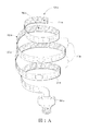
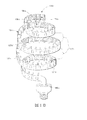
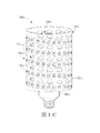
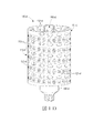
図1A〜1Lは、本明細書中に記載されているアプローチを例示する様々なLED電球100‐a〜100‐lを示している。各LED電球100‐a〜lは、電気コネクタ、例えば、家庭用電源との連結に適している電気コネクタを有する口金180‐a〜180‐lを含む。いくつかの実施形態において、LED電球100‐a〜100‐lは、口金180‐a〜180‐l内に設置されている変圧器、整流器、コンデンサ、AC〜DCおよび/またはDC〜DC電力変換器などの電力調整回路を含むことができる。いくつかの実施形態において、電力調整回路はLED電球100‐a〜100‐lの外部に取り付けられてよい。電源接続は口金180‐a〜180‐l上に配置され、口金のコネクタ部分は、エジソンねじ込み式電球口金または他の標準的電球口金の形態を取ることができる。LED電球100‐a〜100‐lは口金180‐a〜180‐lに連結された少なくとも一の支持構造111‐a〜111‐lを含む。少なくとも一の支持構造111‐a〜111‐lは、開放容積190‐a〜190‐lを有する発光面112‐a〜112‐lの外形を画定する所定の形状に形成される。LED電球100‐a〜100‐lの発光面112‐a〜112‐lの表面積当たりの光出力は、LED電球の外部表面積の1cm2(平方センチメートル)当たりで、好ましくは、約0.3〜30ルーメン、より好ましくは、約0.5〜20ルーメンである。 1A-1L show various LED bulbs 100-a-100-l that illustrate the approaches described herein. Each LED bulb 100-a-l includes a base 180-a-180-l having an electrical connector, for example, an electrical connector suitable for connection to a household power source. In some embodiments, the LED bulbs 100-a-100-l are transformers, rectifiers, capacitors, AC-DC and / or DC-DC power conversions installed in the caps 180-a-180-l. A power adjustment circuit such as a power supply can be included. In some embodiments, the power conditioning circuit may be attached to the exterior of the LED bulbs 100-a to 100-l. The power connections are located on the caps 180-a-180-l, and the connector portion of the cap can take the form of an Edison screw-in bulb cap or other standard bulb cap. The LED bulbs 100-a to 100-l include at least one support structure 111-a to 111-l connected to the caps 180-a to 180-l. The at least one support structure 111-a to 111-l is formed in a predetermined shape that defines the outer shape of the light emitting surfaces 112-a to 112-l having open volumes 190-a to 190-l. The light output per surface area of the light emitting surfaces 112-a to 112-l of the LED bulbs 100-a to 100-l is preferably about 0.3 to 30 per cm 2 (square centimeter) of the external surface area of the LED bulb. Lumen, more preferably about 0.5 to 20 lumen.
LED電球100‐a〜100‐lの全体寸法は同等の明るさの白熱電球に類似している。開放容積190‐a〜190‐lはLED121‐a〜121‐lを冷却するLED電球100‐a〜100‐lを空気の流れを通過させることができるように作用する。 The overall dimensions of the LED bulbs 100-a to 100-l are similar to incandescent bulbs of equivalent brightness. The open volumes 190-a to 190-l serve to allow the air flow to pass through the LED bulbs 100-a to 100-l that cool the LEDs 121-a to 121-l.
LED電球100‐a〜100‐lは、各可撓性のLEDアセンブリが二以上の電気的に接続されたLED121‐a〜121‐lを含む、一以上のLEDアセンブリ120‐a〜120‐lを含む。一以上のLEDアセンブリ120‐a〜120‐l(可撓性および/または長尺および/または直線形であってよい)は、支持構造111‐a〜111‐lの長さに沿って支持構造111‐a〜111‐lに取り付けられかつ物理的に接触している。支持構造111‐a〜111‐lは一以上のLEDアセンブリ120‐a〜120‐lの互いに隣接配置されているセグメント間で開口113‐a〜113‐lを有している。開口113‐a〜113‐lは、一以上のLEDアセンブリ120‐a〜120‐lの互いに隣接配置されているセグメント間で周囲空気が開放容積190‐a〜190‐lへ流入することを可能にする。互いに隣接配置されているセグメント間の空気の流れはLED121‐a〜121‐lを冷却させるように作用することができる。 LED bulbs 100-a to 100-l include one or more LED assemblies 120-a to 120-l, each flexible LED assembly including two or more electrically connected LEDs 121-a to 121-l. including. One or more LED assemblies 120-a-120-l (which may be flexible and / or elongate and / or straight) include support structures along the length of the support structures 111-a-111-l. Attached to and in physical contact with 111-a through 111-l. Support structure 111-a-111-l has openings 113-a-113-l between adjacent segments of one or more LED assemblies 120-a-120-l. Openings 113-a-113-l allow ambient air to flow into open volumes 190-a-190-l between adjacent segments of one or more LED assemblies 120-a-120-l To. The air flow between the segments arranged adjacent to each other can act to cool the LEDs 121-a to 121-l.
いくつかの場合において、一以上のLEDアセンブリ120‐a〜120‐lは、支持構造111‐a〜111‐lの外側(即ち、開放容積190a〜190lの外側)で支持構造111‐a〜111‐lに取り付けることができる。いくつかの場合において、一以上のLEDアセンブリ120‐a〜120‐lは、支持構造111‐a〜111‐lの内側(即ち、開放容積190a〜190lの内側)で支持構造111‐a〜111‐lへ取り付けることができる。一以上のLEDアセンブリ120‐a〜120‐lは、支持構造111‐a〜111‐lの外側および内側で支持構造111‐a〜111‐lに取り付けることができる。 In some cases, one or more of the LED assemblies 120-a-120-l are supported outside the support structures 111-a-111-l (ie outside the open volumes 190a-190l). -L can be attached. In some cases, the one or more LED assemblies 120-a-120-l are supported inside the support structures 111-a-111-l (ie, inside the open volumes 190a-190l). Can be attached to -l. One or more LED assemblies 120-a-120-l may be attached to the support structures 111-a-111-l outside and inside the support structures 111-a-111-l.
いくつかの構成において、支持構造111‐a〜111‐lは第1の主要表面とこれに対向する第2の主要表面を有している。一以上のLEDアセンブリ120‐a〜120‐lは長尺の支持構造の第1の主要表面に配置されている。いくつかの構成において、一以上のLEDアセンブリ120‐a〜120‐lは、第1の主要表面に沿って配置された少なくとも第1のLEDアセンブリと、支持構造の第2の主要表面に沿って配置された少なくとも第2のLEDアセンブリと、を含む。 In some configurations, support structures 111-a-111-l have a first major surface and a second major surface opposite thereto. One or more LED assemblies 120-a-120-l are disposed on the first major surface of the elongated support structure. In some configurations, the one or more LED assemblies 120-a-120-l include at least a first LED assembly disposed along the first major surface and a second major surface of the support structure. And at least a second LED assembly disposed.
いくつかの構成において、支持構造は第1の端部および第2の端部を有する長尺の構造を含み、第1および第2の端部は口金に直接取り付けられる。いくつかの他の構成において、第1の端部は口金に直接取り付けられ、第2の端部は口金から離間されている。 In some configurations, the support structure includes an elongated structure having a first end and a second end, the first and second ends being directly attached to the base. In some other configurations, the first end is attached directly to the base and the second end is spaced from the base.
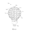
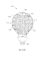
図1Aおよび図1Bは、支持構造111‐a〜111‐bが螺旋構造に形付けられる実施形態を示している。支持構造が単一の連続エレメントである場合もあれば、支持構造は複数の個別の支持エレメントを含む場合もある。支持構造はその中で穴を切断したかまたは形成した固体形態であってよい;支持構造はフレームエレメント同士間で互いから離間されているフレームであってよい;例えば、支持構造は網目(メッシュ)状であってもよい。相互に接続されたLED121‐a〜121‐lを有する単一の連続したLEDアセンブリは連続または個別のエレメント支持構造上に配置することができる。いくつかの実施形態において、複数のLEDアセンブリは連続または個別のエレメント支持構造上に配置することができる。いくつかの実施形態において、図1A、図1B、図1G、図1Hに示したように、支持構造111‐a、111‐b、111‐g、111‐h、111‐k、111‐lによって画定された表面112‐a、112‐b、112‐g、112‐hによって画定された光容積(形状)は、約0.5よりもさらに約0.7よりも大なる球度を有することができる。 1A and 1B show an embodiment in which the support structures 111-a-111-b are shaped into a helical structure. The support structure may be a single continuous element or the support structure may include a plurality of individual support elements. The support structure may be in solid form with holes cut or formed therein; the support structure may be a frame spaced from each other between the frame elements; for example, the support structure may be a mesh It may be a shape. A single continuous LED assembly having interconnected LEDs 121-a-121-l can be placed on a continuous or separate element support structure. In some embodiments, multiple LED assemblies can be placed on a continuous or separate element support structure. In some embodiments, as shown in FIGS. 1A, 1B, 1G, and 1H, by support structures 111-a, 111-b, 111-g, 111-h, 111-k, 111-l. The light volume (shape) defined by the defined surfaces 112-a, 112-b, 112-g, 112-h has a sphericity greater than about 0.5 and even greater than about 0.7. Can do.
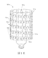
いくつかの実施形態において、図1C〜図1Fに示したように、支持構造は円筒形であってよい。図1Cおよび図1Dに示したように、開口113‐c、113‐dは円筒形支持体111‐c、111‐dに形成された穴でもよい。図1E、図1Fに示したように、支持構造111‐e、111‐fは円筒形フレームであり、開口113‐e、113‐fはフレームエレメント間のスペースである。 In some embodiments, the support structure may be cylindrical, as shown in FIGS. 1C-1F. As shown in FIGS. 1C and 1D, the openings 113-c and 113-d may be holes formed in the cylindrical supports 111-c and 111-d. As shown in FIGS. 1E and 1F, the support structures 111-e and 111-f are cylindrical frames, and the openings 113-e and 113-f are spaces between the frame elements.
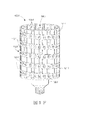
いくつかの実施形態において、図1Iおよび図1Jに示したように、支持構造111‐iと111‐jは円錐形状を画定する。いくつかの実施形態において、図1Kおよび図1Lに示したように、支持構造111‐k、111‐lはメッシュ状に形成されてもよい。LEDアセンブリ120‐k、120‐lはマイクロLEDを含むことができる。 In some embodiments, as shown in FIGS. 1I and 1J, support structures 111-i and 111-j define a conical shape. In some embodiments, as shown in FIGS. 1K and 1L, the support structures 111-k, 111-l may be formed in a mesh. The LED assemblies 120-k, 120-l may include micro LEDs.
支持構造111‐a〜111‐lは、LED電球100‐a〜100‐lに対して形状および剛性を提供するとともにLED電球100‐a〜100‐lに熱的および/または光学特性を付与することもできる。支持構造は、金属、プラスチック、成型プラスチック、および/またはいくつかの材料の複合材料で作ることができる。支持構造が金属それ自体であるかまたは金属を含む実施形態において、金属は陽極酸化、酸化されるか、或いは、適切な塗膜材料で塗膜することができる。 The support structures 111-a to 111-l provide shape and rigidity to the LED bulbs 100-a to 100-l and impart thermal and / or optical properties to the LED bulbs 100-a to 100-l. You can also The support structure can be made of metal, plastic, molded plastic, and / or a composite of several materials. In embodiments where the support structure is the metal itself or comprises a metal, the metal can be anodized, oxidized, or coated with a suitable coating material.
いくつかのインプリメンテーションによれば、支持構造は硬化された構造的塗膜を含む。硬化された構造的塗膜は熱硬化性材料、放射線硬化物、例えば、UV硬化ポリマまたはUV硬化系エポキシなどのUV硬化材料を含むことができる。硬化された塗膜は、雲母、銀、金および/または銅粒子などの金属粒子を含むことができる。 According to some implementations, the support structure includes a cured structural coating. The cured structural coating can include a thermosetting material, a radiation cured material, for example, a UV curable material such as a UV curable polymer or a UV curable epoxy. The cured coating can include metal particles such as mica, silver, gold and / or copper particles.
硬化された構造的塗膜を含む実施形態において、構造的塗膜はLEDから発生した熱を消散させるように構成することができる。硬化された構造的塗膜はLEDの少なくとも一部の上に配置され、LEDから発生した光を透過するように構成することができる。いくつかの場合において、硬化された塗膜はLEDから発せられた光を方向付けるレンズを形成する。硬化された構造的塗膜は、同じ大きさのテクスチャ処理されていない表面に比べて有効表面積が少なくとも3倍も大きい表面テクスチャを有する、(開放容積の内側または外側の)周囲空気へ露出される表面を有することができる。 In embodiments that include a cured structural coating, the structural coating can be configured to dissipate the heat generated from the LED. The cured structural coating may be disposed on at least a portion of the LED and configured to transmit light generated from the LED. In some cases, the cured coating forms a lens that directs light emitted from the LED. The cured structural coating is exposed to ambient air (inside or outside the open volume) having a surface texture that has an effective surface area that is at least three times greater than an untextured surface of the same size. Can have a surface.
支持構造111‐a〜111‐lは、約100W/mKより、約250W/mKより、さらには約300W/mKより高い熱伝導率を有することができる。いくつかの実施形態において、図1B、1D、1F、1H、1J、1Lに示したように、支持構造111‐b、111‐d、111‐f、111‐h、111‐j、111‐lはLEDから発生した熱を消散させるように構成されている冷却構造130‐b、130‐d、130‐f、130‐h、130‐j、130‐l、例えば、冷却フィンを有することができる。冷却構造は、図1Hおよび図1Jに示したように、支持構造の外側(即ち、開放容積の外側)に配置され、および/または、図1B、図1D、図1F、図1Lに示したように、支持構造の内側(即ち、開放容積の内側)に配置することができる。 Support structures 111-a through 111-l can have a thermal conductivity greater than about 100 W / mK, greater than about 250 W / mK, and even greater than about 300 W / mK. In some embodiments, as shown in FIGS. 1B, 1D, 1F, 1H, 1J, 1L, support structures 111-b, 111-d, 111-f, 111-h, 111-j, 111-l. Can have cooling structures 130-b, 130-d, 130-f, 130-h, 130-j, 130-1 configured to dissipate heat generated from the LEDs, for example, cooling fins . The cooling structure is located outside the support structure (ie outside the open volume) as shown in FIGS. 1H and 1J and / or as shown in FIGS. 1B, 1D, 1F, 1L. And inside the support structure (ie inside the open volume).
いくつかの実施形態において、支持構造の少なくとも一の主要表面は、同一の大きさと形状を有するテクスチャが処理されていない表面より表面積が少なくとも3倍も大きい表面テクスチャを有している。支持構造表面のテクスチャ処理は、支持構造へある特定の光学的および/または熱的特性を付与するために使用することができる。 In some embodiments, at least one major surface of the support structure has a surface texture that has a surface area that is at least three times greater than the untreated surface having the same size and shape. Texture treatment of the support structure surface can be used to impart certain optical and / or thermal properties to the support structure.
いくつかの実施形態において、支持構造は、例えば、約320nm〜700nmの波長の可視光に対して85%より高い反射率を有している。支持構造は、材料を含み、および/または、LED121‐a〜121‐lによって発せられる光を散乱させるように構成された表面テクスチャを有している。 In some embodiments, the support structure has a reflectivity greater than 85%, for example, for visible light having a wavelength of about 320 nm to 700 nm. The support structure includes a material and / or has a surface texture configured to scatter light emitted by the LEDs 121-a through 121-l.
LED電球100‐a〜100‐lの各々は複数の相互に電気接続されたLED121‐a〜121‐1を含む一以上のLEDアセンブリ120‐a〜120‐lを含む。いくつかの実施形態において、各LEDサブアセンブリは、複数のLEDを配列した基板、例えば、可撓性基板を含む。例えば、LEDは基板の長さに沿って単列または二以上の列を成して配列することができる。LEDは電気的に直列接続または並列接続することができる。LEDアセンブリの基板は第1の主要表面とこれに対向する主要表面を有している。いくつかのインプリメンテーションにおいて、LED121‐a〜121‐lの各々は基板の主要表面にほぼ垂直を成す発光面またはエッジを有することができる。いくつかのインプリメンテーションにおいて、LED121‐a〜121‐lの各々は基板の主要表面にほぼ平行を成す発光面またはエッジを有することができる。いくつかの態様によれば、第1の群のLEDは電気的に連結されて比較的低い光出力を提供し、第2の群のLEDは電気的に連結されて比較的高い光出力を提供する。 Each of the LED bulbs 100-a to 100-l includes one or more LED assemblies 120-a to 120-l including a plurality of mutually electrically connected LEDs 121-a to 121-1. In some embodiments, each LED subassembly includes a substrate on which a plurality of LEDs are arranged, eg, a flexible substrate. For example, the LEDs can be arranged in a single row or two or more rows along the length of the substrate. The LEDs can be electrically connected in series or in parallel. The substrate of the LED assembly has a first major surface and a major surface opposite thereto. In some implementations, each of the LEDs 121-a-121-l can have a light emitting surface or edge that is substantially perpendicular to the major surface of the substrate. In some implementations, each of the LEDs 121-a-121-l can have a light emitting surface or edge that is substantially parallel to the major surface of the substrate. According to some aspects, the first group of LEDs are electrically coupled to provide a relatively low light output, and the second group of LEDs are electrically coupled to provide a relatively high light output. To do.
いくつかの実施形態において、LEDアセンブリの基板は可撓性のプリント回路基板を含み、LEDは表面実装LEDを含む。いくつかの実施形態において、図1Kおよび1Lに示したように、LED121‐k、121‐lはマイクロLEDを含む。マイクロLEDは集積回路内において共に形成された数多くのLEDであり、これらは可撓性であってよい。 In some embodiments, the substrate of the LED assembly includes a flexible printed circuit board and the LED includes a surface mount LED. In some embodiments, as shown in FIGS. 1K and 1L, LEDs 121-k, 121-l include micro LEDs. A micro LED is a number of LEDs formed together in an integrated circuit, which may be flexible.
いくつかのインプリメンテーションにおいて、一以上の塗膜は、LEDアセンブリ120‐a〜120‐lの少なくとも一部を覆って配置することができる。様々な構成において、塗膜は、周囲空気、例えば、開放容積190‐a〜190‐lの外側または内側に露出される表面を有している。塗膜は、セラミック、ガラス、ポリマ、プラスチック、金属粉末の一以上を含むことができる。例えば、塗膜はある特定の光学的および/または熱的特性を提供するように構成されている。いくつかの場合において、塗膜表面は、同じ大きさのテクスチャ処理されていない表面より表面積が少なくとも3倍も大きい表面テクスチャを有している。塗膜は、LEDから発生された光を透過および/または散乱させるように構成することができる。塗膜は、LEDから発せられた光を方向付けるように構成されたレンズを形成することができる。これに加えてまたはこれに代えて、LED電球は支持構造上に配置されている少なくとも一の熱拡散層または塗膜を含むことができる。 In some implementations, one or more coatings can be placed over at least a portion of the LED assemblies 120-a-120-l. In various configurations, the coating has a surface that is exposed to ambient air, eg, outside or inside the open volumes 190-a to 190-l. The coating can include one or more of ceramic, glass, polymer, plastic, metal powder. For example, the coating is configured to provide certain optical and / or thermal properties. In some cases, the coating surface has a surface texture that is at least three times as large in surface area as an untextured surface of the same size. The coating can be configured to transmit and / or scatter light generated from the LED. The coating can form a lens configured to direct the light emitted from the LED. In addition or alternatively, the LED bulb may include at least one thermal diffusion layer or coating disposed on the support structure.
いくつかの態様によれば、LED電球はLED上に配置された光シートを更に含む。光シートはLEDから発せられた光を拡散するように構成することができる。光シートは、光シートから光を透過させる前に、LEDから発せられた光を光シートを通過する光路に沿って導くように構成することができる。いくつかのインプリメンテーションにおいて、光シートはLEDアセンブリ上に配置されている塗膜に埋め込まれる。 According to some aspects, the LED bulb further includes a light sheet disposed on the LED. The light sheet can be configured to diffuse the light emitted from the LED. The light sheet can be configured to guide light emitted from the LEDs along an optical path that passes through the light sheet before allowing light to pass through the light sheet. In some implementations, the light sheet is embedded in a coating disposed on the LED assembly.
図2Aおよび図2Bは、可撓性基板210とこの可撓性基板に沿って互いに離間されているLED(複数)220とを含むLEDアセンブリの部分を示している。図2Aにおいて、LED220は基板210上に単列配列される。図2Bは可撓性基板210上に2列のLED220が配列されている他のLEDアセンブリ形式を示している。LEDが任意の好適なパターンで可撓性基板に沿って配列することができることが理解されよう。パターンは所望の配光および/または放熱の仕様を提供するように選択することができる。
2A and 2B show a portion of an LED assembly that includes a
可撓性基板210はLED220と口金電子部品の間の電気的接続を容易にする可撓性回路基板であってよい。図2Aおよび図2Bに示したように、導電体230は可撓性基板内または上に配置され、可撓性基板の長さに沿って延出されてLED220の各々を口金内に配置された口金電子部品に電気的接続させる(図1Aおよび1Bに示す)。LED220は可撓性基板に半田付けされる表面実装LEDを含むことができるかまたはマイクロLEDであってもよい。
The
ここで、図3Aおよび3Bを参照するに、LEDは、矢印350によって概念的に示したように、表面またはエッジから発光する。図3Aに示したように、LED320の発光面またはエッジ321が可撓性基板310の主要表面311に対してほぼ平行を成すようにLED320の一以上が可撓性基板310上に配列される。図3Bに示したように、いくつの場合において、LED330の発光面またはエッジ331が可撓性基板310の主要表面311に対してほぼ垂直を成すようにLED330の一以上は可撓性基板310上に配列される。いくつかの構成において、図3Cに示したように、LED320の一部が可撓性基板310の主要表面311とほぼ平行を成す発光面321から光350を発し、LED330一部が主要表面311にほぼ垂直を成すかまたは傾斜している発光面331から光350を発するように、LED320、330が可撓性基板310上に共に配列される。
Referring now to FIGS. 3A and 3B, the LED emits light from the surface or edge, as conceptually indicated by
様々なLED電球の構成によれば、一以上のLEDアセンブリは支持構造に取り付けるかおよび/または一体化させることができる。図4は、いくつかの実施形態によるLED照明装置を形成するためのプロセスを示す流れ図である。複数の相互に電気接続されたLEDが配置されている基板を含むLEDアセンブリは支持構造に連結される(ステップ410)。支持構造は電球の形状に形成され(ステップ420)、発光面と開放容積を画定する。LED電球の形状は一以上のLEDアセンブリのセグメントの周りと隣接しているセグメント間の通気を可能にする。発光面はLEDから発せられた光の所望の配光を提供する。いくつかの実施形態において、形成し取り付けることは、少なくとも一のLEDアセンブリを取り付ける前に、支持構造を所定の形状に形成することを含む。他の実施形態において、形成し取り付けることは、少なくとも一のLEDアセンブリを取り付けた後で、支持構造を所定の形状に形成することを含む。支持構造を形成することは、畳み込み、折曲げ、成形および硬化の一以上を含むことができる。支持構造が硬化によって剛性または半剛性の状態に硬化される場合、支持構造は所定の形状に形成された後に硬化される。 According to various LED bulb configurations, one or more LED assemblies can be attached to and / or integrated with a support structure. FIG. 4 is a flow diagram illustrating a process for forming an LED lighting device according to some embodiments. An LED assembly including a substrate on which a plurality of interconnected LEDs are disposed is coupled to a support structure (step 410). The support structure is formed in the shape of a light bulb (step 420) and defines a light emitting surface and an open volume. The shape of the LED bulb allows for ventilation around and adjacent segments of one or more LED assemblies. The light emitting surface provides the desired light distribution of the light emitted from the LED. In some embodiments, forming and attaching includes forming the support structure into a predetermined shape prior to attaching at least one LED assembly. In other embodiments, forming and attaching includes forming the support structure in a predetermined shape after attaching at least one LED assembly. Forming the support structure can include one or more of folding, folding, shaping, and curing. When the support structure is cured into a rigid or semi-rigid state by curing, the support structure is cured after being formed into a predetermined shape.
様々なインプリメンテーションによれば、LEDアセンブリは、長尺の支持構造に沿って長手方向に配列され、例えば、積層、接着、または他の適切なプロセスによって、支持構造に取り付けることができる。いくつかの場合において、LEDアセンブリの幅は支持構造の幅に等しい(またはほぼ等しい)。支持構造は、電球の形状に折曲され、畳み込まれ、成形され、および/または、硬化される。支持構造は、多くの場合、更なる支持を必要とせずに、支持構造を立設保持する口金に機械的に取り付けられる。LEDは口金電子部品に電気的に連結される。 According to various implementations, the LED assemblies can be arranged longitudinally along an elongated support structure and attached to the support structure, for example, by lamination, bonding, or other suitable process. In some cases, the width of the LED assembly is equal (or approximately equal) to the width of the support structure. The support structure is folded, folded, molded and / or cured into the shape of a light bulb. The support structure is often mechanically attached to a base that holds the support structure upright without requiring further support. The LED is electrically connected to the base electronic component.
いくつかのインプリメンテーションにおいて、可撓性LEDアセンブリは円筒形上で螺旋状に機械的に巻回することができる。円筒形は、(LEDアセンブリが取り付けられた)基部の形状を膨張させて電球形状を形成するために切断され、例えば、レーザーカットされるか、または、可撓性基板のエッジに沿って機械加工される。その後、可撓性LEDアセンブリは既に螺旋形にカットされ膨張されている剛性または半剛性の形状において支持される。 In some implementations, the flexible LED assembly can be mechanically wound helically on a cylinder. The cylinder is cut to expand the shape of the base (with the LED assembly attached) to form a bulb shape, for example laser cut or machined along the edge of a flexible substrate Is done. The flexible LED assembly is then supported in a rigid or semi-rigid shape that has already been cut and expanded into a spiral.
支持構造に適した材料は、金属、プラスチック、セラミック硬化性樹脂などの所望の電球形状に合わせて形成することができる材料、および/または、層、部分、および/または様々な材料の混合材料を含む複合材料を含む。支持構造に金属を使用する場合、金属は、例えば、耐久性を高めるために陽極酸化されてもよいし、または、酸化されてもよい。いくつかの実施形態において、支持構造の表面は、エンボス加工、エッチング、サンドブラストなどによってテクスチャ処理されることで支持構造表面の有効表面積を大きくすることができる。表面テクスチャ処理は有効表面積を有意に大きくすることができる。例えば、支持構造の表面のテクスチャは、同じ大きさで同一材料のテクスチャ処理されていない表面積に比べて有効表面積が少なくとも3倍に相当する表面粗さを有することができる。表面テクスチャは、テクスチャ処理されていない表面に比べて、更なる放熱および/または更なる光拡散や光散乱を提供することができる。例えば、テクスチャ処理後の表面粗さ(Ra)は、同じ大きさのテクスチャ処理されていない表面の少なくとも2倍〜3倍に相当する表面粗さを達成することができる。 Suitable materials for the support structure include materials that can be formed to the desired bulb shape, such as metals, plastics, ceramic curable resins, and / or mixed materials of layers, portions, and / or various materials. Including composite materials. When using a metal for the support structure, the metal may be anodized or oxidized, for example, to increase durability. In some embodiments, the surface of the support structure can be textured by embossing, etching, sandblasting, etc. to increase the effective surface area of the support structure surface. Surface texturing can significantly increase the effective surface area. For example, the texture of the surface of the support structure can have a surface roughness corresponding to at least three times the effective surface area compared to an untextured surface area of the same size and material. A surface texture can provide additional heat dissipation and / or additional light diffusion and / or light scattering compared to an untextured surface. For example, the textured surface roughness (Ra) can achieve a surface roughness equivalent to at least 2 to 3 times that of an untextured surface of the same size.
支持構造はLEDアセンブリを支持するだけでなくLED電球に対する放熱および/または光管理を提供するように構成されている。いくつかの場合において、支持構造はヒートシンクである。熱拡散層、例えば、約100W/mKより、約250W/mKより、さらには約300W/mKより高い熱伝導率を有する材料の一以上の層は、支持構造の片面または両面および/または片方または両方のエッジに塗布することができる。支持構造(および/またはその上に配置された塗膜)は、個々のLEDから発せられた光を拡散し反射し透過し均質化しおよび/または混合するために使用され、指定された光の分光(スペクトル)および/または強度分布を提供することができる。例えば、支持構造は、反射面を有し、反射層によって塗膜され、光を拡散するためにテクスチャ処理され、或いは、LEDから発せられた光を管理するように配列することができる。支持構造が反射面を有しまたは反射層が支持構造上に配置されている実施形態において、表面や層の反射率は、LEDから発せられた光の波長、例えば、約320nm〜約700nmに対して、約85%より高い。支持構造が光透過面を有しまたは透過層が支持構造上に配置されている実施形態において、表面や層の透過率は、LEDから発せられた光の波長、例えば、約320nm〜約700nmに対して約85%より高い。 The support structure is configured to support the LED assembly as well as provide heat dissipation and / or light management for the LED bulb. In some cases, the support structure is a heat sink. The thermal diffusion layer, for example, one or more layers of a material having a thermal conductivity greater than about 100 W / mK, greater than about 250 W / mK, and even greater than about 300 W / mK can be provided on one or both sides of the support structure and / or Can be applied to both edges. The support structure (and / or the coating disposed thereon) is used to diffuse, reflect, transmit, homogenize and / or mix the light emitted from the individual LEDs, with the specified light spectrum. (Spectrum) and / or intensity distribution can be provided. For example, the support structure may have a reflective surface and be coated with a reflective layer, textured to diffuse light, or arranged to manage light emitted from the LED. In embodiments where the support structure has a reflective surface or the reflective layer is disposed on the support structure, the reflectivity of the surface or layer is relative to the wavelength of light emitted from the LED, for example from about 320 nm to about 700 nm. Higher than about 85%. In embodiments where the support structure has a light transmissive surface or a transmissive layer is disposed on the support structure, the surface or layer transmittance is at a wavelength of light emitted from the LED, for example, from about 320 nm to about 700 nm. On the other hand, it is higher than about 85%.
これに加えてまたはこれに代えて、支持構造表面(またはその上に配置された塗膜層)は照明装置へ光散乱を提供するように構成することができる。いくつかの場合において、光散乱は、支持構造および/またはLEDアセンブリ上に配置された塗膜によって提供することができる。適切な塗膜は、例えば、反射性金属、ガラス、透明プラスチックなどを含むことができる。様々な実施形態によれば、一以上のタイプの塗膜が様々な特性を有する照明構造を提供するために使用される。例えば、ある塗膜はLEDから発生する熱を消散するために選択することができる。別の塗膜は一以上の光学特性を提供するように選択することができる。塗膜は支持構造およびLEDアセンブルの片面または両面に塗布することができる。 In addition or alternatively, the support structure surface (or coating layer disposed thereon) can be configured to provide light scattering to the lighting device. In some cases, light scattering can be provided by a coating disposed on the support structure and / or the LED assembly. Suitable coatings can include, for example, reflective metals, glasses, transparent plastics, and the like. According to various embodiments, one or more types of coatings are used to provide lighting structures having various properties. For example, a coating can be selected to dissipate the heat generated from the LED. Another coating can be selected to provide one or more optical properties. The coating can be applied to one or both sides of the support structure and LED assembly.
いくつかの実施形態において、方法は、LEDの発光面上に光シートを配列することを含む。いくつかの実施形態において、光学的または熱的な層は、LEDアセンブリの主要表面と構造的支持体の主要表面の片面または両面に付着させることができる。例えば、付着された層は光学的または熱的に拡散性であってよい。光学的な層が付着される場合、光学的な層は光透過、光反射および光拡散の一以上を提供する材料を含むことができる。 In some embodiments, the method includes arranging a light sheet on the light emitting surface of the LED. In some embodiments, the optical or thermal layer can be applied to one or both of the major surface of the LED assembly and the major surface of the structural support. For example, the deposited layer may be optically or thermally diffusive. If an optical layer is deposited, the optical layer can include materials that provide one or more of light transmission, light reflection, and light diffusion.
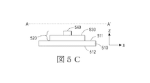
図5A〜5Gは様々な支持構造/LEDアセンブリ構成を例示している斜視および断面図である。いくつかの場合において、支持構造は図5Aの斜視図に示した実施例と同様にほぼ平坦である。支持構造とLEDアセンブリ構成の一部を示す同図において、可撓性基板530と複数のLED540とを含むLEDアセンブリ520は支持構造510の一つの平坦な面に連結される。図5Aは基準座標に対するLEDアセンブリの配向を示している。以下の図でも同様にこの配向を使用する。可撓性基板530の(図5Aのy方向に沿った)長さは(図5Aのx方向に沿った)幅よりはるかに大である。同様に、支持構造510の(図5Aのy方向に沿った)長さは(図5Aのx方向に沿った)幅よりはるかに大である。図5Aに示したように、可撓性基板530は支持構造に沿って長手方向に配列されている。可撓性基板と支持構造の長さおよび/または幅は、図5Aに示したものにほぼ等しいものでよい。可撓性基板530は、第1の主要表面531、これに対向する主要表面532、大エッジ535、これに対向する大エッジ536、小エッジ533、およびこれに対向する小エッジ534を有している。
5A-5G are perspective and cross-sectional views illustrating various support structure / LED assembly configurations. In some cases, the support structure is substantially flat, similar to the embodiment shown in the perspective view of FIG. 5A. In the figure showing a support structure and a portion of the LED assembly configuration, an
図5Bによって示されるいくつかの実施形態において、一以上のLEDアセンブリ520が支持構造510に連結されている。図5Aおよび図5Bによる実施例は、支持構造の幅を横切るx方向に沿って平面状でありまたは平坦である支持構造を含む。この構成は本明細書中で「平坦な支持構造」と称され、その幅方向(即ち、その小寸法)に平面状である支持構造を指すが、支持構造はその長さに(即ち、その大寸法)沿って平坦ではないことを理解されたい。言い換えれば、支持構造は、その長手方向に、畳み込まれ、成形され、折曲され、或いは、他の方法で形成されることにて、図1Aおよび図1Bに示した形状のような電球形状を形成することができる。
In some embodiments illustrated by FIG. 5B, one or
図5Cは、図5Aに示した支持構造/LEDアセンブリ構成を示す断面図であり、図中、断面はA‐A′に沿って切断されている。支持構造は必要に応じて、一以上のテクスチャ処理された表面511、512を含む場合もある。
FIG. 5C is a cross-sectional view of the support structure / LED assembly configuration shown in FIG. 5A, where the cross-section is cut along AA ′. The support structure may include one or more
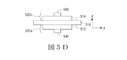
図5Dは、支持構造510の第1の表面513に連結された第1のLEDアセンブリ520aと第1の表面に対向する支持構造の第2の表面514に連結された第2のLEDアセンブリ520bとを有する平坦な支持構造512を示している。
FIG. 5D illustrates a
支持構造は(図5Eに示した)凸支持構造551または(図5Fに示した)凹状の支持構造であってよい。図5Eは(可撓性基板530とLED540を含む)LEDアセンブリ520が支持構造551の凸面に連結されている実施例を示している。図5Fは、支持構造552の凹面に連結されたLEDアセンブリ520を示している。
The support structure may be a convex support structure 551 (shown in FIG. 5E) or a concave support structure (shown in FIG. 5F). FIG. 5E shows an embodiment in which the LED assembly 520 (including the
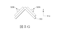
いくつかの場合において、複数のLEDアセンブリは、図5Gに示したように、支持構造の異なるファセット上に配置することができる。三角形の支持構造553は、第1のファセット553a上で第1のLEDアセンブリ520aを支持し、第2のファセット553b上で第2のLEDアセンブリ520bを支持している。本明細書中に提供されている実施例は可能性のある数多くの支持構造/LEDアセンブリ構成のほんの一部であることが理解されよう。
In some cases, multiple LED assemblies can be placed on different facets of the support structure, as shown in FIG. 5G. The
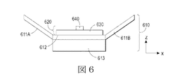
前述したように、支持構造は、金属、金属合金、プラスチック、または所望されるLED電球形状に形成するために適している任意の他の材料を含むことができる。いくつかの場合において、支持構造は、複数の層、複数の部分および/または複数の材料を含む複合構造であってよい。複合支持構造の異なる層、部分または材料は支持構造へ異なる特性を付与することができる。例えば、層、部分および/または材料は構造特性を付与するために使用され、層、部分および/または材料はさらに構造的および熱的特性を付与するために使用され、層、部分および/または材料は構造的および光学的特性を付与するために使用されることができる。いくつかの場合において、複合支持構造は、複数の材料、例えば、プラスチックマトリックスに埋め込まれた金属粒子を含む層または構成要素を含むことができる。いくつかの場合において、複合支持構造は、図6に示したように、異なる材料から作製される複数の層および/または複数の部分を含むことができる。図6に示した複数の層および部分の各々は構造的支持体の構造的特性に寄与することができる。 As described above, the support structure can include metal, metal alloy, plastic, or any other material suitable for forming into the desired LED bulb shape. In some cases, the support structure may be a composite structure including multiple layers, multiple portions, and / or multiple materials. Different layers, portions or materials of the composite support structure can impart different properties to the support structure. For example, layers, portions and / or materials are used to impart structural properties, and layers, portions and / or materials are further used to impart structural and thermal properties, layers, portions and / or materials. Can be used to impart structural and optical properties. In some cases, the composite support structure can include a plurality of materials, eg, layers or components that include metal particles embedded in a plastic matrix. In some cases, the composite support structure can include multiple layers and / or multiple portions made from different materials, as shown in FIG. Each of the plurality of layers and portions shown in FIG. 6 can contribute to the structural properties of the structural support.
図6は、支持構造610が複数の層612、613と部分611a、611bからなる複合体である支持構造/LEDアセンブリの組合せを示している。(可撓性基板630とLED640を含む)LEDアセンブリ620は支持構造610上に配置される。支持構造は構造的支持を付与する比較的厚肉の非金属層、例えば、プラスチック層613と、支持体610の構造特性に寄与し、さらにLED640から発生する熱の消散および/または分布をも提供する比較的薄肉の金属層312と、を含む。反射性部分611a、611b(例えば、プラスチックおよび/または金属製反射器)は支持体610の構造特性に寄与しLED640から発せられた光を反射する。
FIG. 6 shows a support structure / LED assembly combination in which the
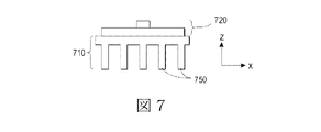
前述したように、構造的支持体は所望される特性を提供する表面テクスチャを含むことができる。これに加えまたはこれに代えて、支持構造は、図6に示した反射体部分611a、611bなどの所望される特性を提供する機能や部分を含むことができる。図7は、任意の機能を有する支持構造の他の実施例を示している。この実施例において、支持構造710は、LEDアセンブリ720が配列された面の反対側の支持構造の面上に配置されたヒートシンクフィン750を含む。フィン750は支持構造710の幅および/または長さに沿って延び、支持構造に対して剛性および除熱能力の一方または両方を付与するように設計することができる。
As previously mentioned, the structural support can include a surface texture that provides the desired properties. In addition or alternatively, the support structure can include features or portions that provide desired characteristics, such as the reflector portions 611a, 611b shown in FIG. FIG. 7 shows another embodiment of a support structure having an arbitrary function. In this example, the
(構造特性に寄与するともしないともいえない)任意の塗膜、層、および/または、シートは支持構造およびLEDアセンブリと併用することができる。図8は使用することか可能であるいくつかの任意の塗膜を示している。LEDアセンブリ820の部分および/または支持構造810の部分は可撓性基板830の少なくとも一部および/またはLED840の一部を被覆する光塗膜850によって塗膜することができる。例えば、光塗膜850は、LED電球が同様の形状ファクタと明るさを有する白熱光の配光にほぼ近いかまたはこれに匹敵する配光を提供するように複数のLED840から出射する光を拡散または均質化するように作用することができる。塗膜850は、放熱および/または光拡散を提供する表面テクスチャ851を有することができる。前述のように、表面テクスチャ851は、同じ材料、同じ大きさ、同じ形状のテクスチャ処理されていない表面より3倍も大きい有効表面積を提供することができる。
Any coating, layer, and / or sheet (which may or may not contribute to structural properties) can be used in conjunction with the support structure and the LED assembly. FIG. 8 shows some optional coatings that could be used. A portion of the
図8の構成は、構造的支持体810上に配置された熱伝導層860を含む。この特定の実施例において、LEDアセンブリは支持構造810の第1の表面811に沿って配置され、熱伝導層860は支持構造810の対向する第2の表面812上に配置される。他の構成において、熱伝導層は,LEDアセンブリと同一面上に配置されるか、または、支持構造の両面上に配置される。
The configuration of FIG. 8 includes a thermally
図8に示した構成は、構造的支持体810の第1の表面811上に配置された蛍光体層870を含む。蛍光体層はLEDから発せられる光とは異なる波長で発光することができる蛍光材料を含む。LEDと蛍光体層から発せられる光は、LED電球から出射する光に対してより広範な分光特性を提供することができる。例えば、LEDは青色光を発光し、黄色蛍光体は構造支持体上に塗膜されるかおよび/または塗膜850に埋め込まれる。
The configuration shown in FIG. 8 includes a
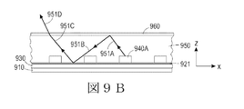
いくつかの実施形態において、光塗膜および/または光シートは、光が導波路外で結合されるまでLEDアセンブリに沿った距離にわたって導光するために、導波路として、LEDを覆って配置することができる。図9AはLEDアセンブリ920を配置した構造的支持体910を示している。塗膜950はLED940上に配置される。光塗膜/空気界面952における塗膜950と空気の屈折率の差によってLED940から発せられた光の少なくとも一部に対して界面952で全内反射(TIR)がもたらされる。図9Aは、LED940aから出射し塗膜面951と可撓性基板930との間で、ある距離にわたって、導光される光ビーム950を示している。矢印951aはLED940aから出射する光を表している。光は界面952において矢印951bに沿って反映される。光は矢印951cに沿って(反射性塗膜921を含むことができる)可撓性基板930の表面で再反射する。塗膜/空気の界面に入射する光の角度が全内反射(TIR)の臨界角より小なる場合、最終的に光は矢印951dに沿って塗膜から出射する。図9Bは多くの点で図9Aに類似している。図9BはLEDから発せられる光を導くかまたは導波することを容易くするためにLEDを積層し得る光シートを示している。この実施例において、光シートと空気の間、または、光シートと塗膜の間の界面は出射光に対してTIR界面を提供する。
In some embodiments, the light coating and / or light sheet is placed over the LED as a waveguide to guide light over a distance along the LED assembly until light is coupled out of the waveguide. be able to. FIG. 9A shows a
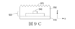
図9Cおよび9Dに示すように、光塗膜および/または光シートは、LEDから発せられる光を方向付ける線形プリズム970および/またはレンズやレンズ構造980などの様々な表面特性970、980を有する光方向付け面を形成するかまたは含むことができる。
As shown in FIGS. 9C and 9D, the light coating and / or light sheet is a light having
いくつかの実施形態において、LEDアセンブリは所定の形状に形成され、硬化性塗膜はLEDアセンブリの少なくとも一部の上に配置される。硬化後、硬化された構造的塗膜はLEDアセンブリを所定の形状に維持するために使用される。図10は、いくつかの実施形態に基づいてLED電球を形成するプロセスを記述している流れ図である。複数のLEDが配置された可撓性基板を含むLEDアセンブリが所定の形状に形成される(ステップ1010)。例えば、LEDアセンブリは、同等の明るさの白熱電球の大きさと全体的な形状が類似している螺旋形に配置することができる。剛性または半剛性の支持体に硬化することができる硬化性塗膜は、例えば、様々な塗膜プロセスまたはオーバーモールド(外側被覆)によって、LEDアセンブリに塗布される(ステップ1020)。硬化性塗膜は、硬化性ポリマ、硬化性プラスチック、または硬化性複合体を含むかまたはこれら自体であってよい。硬化性複合体は、硬化性ポリマーマトリックス中に粒子を含有する樹脂を含むことができる。粒子は硬化された構造的塗膜の様々な光学的または熱的特性を提供または改善することができる。例えば、硬化性ポリマーマトリックス中に埋め込まれた金属粒子はLEDから発生する熱の放熱を改良することができる。マトリックス中に埋め込まれた光学粒子は光の拡散(および/または他の光学特性)を大きくすることができる。硬化性塗膜は、熱硬化、(UV放射などの)放射露光、電子ビーム露光によって硬化可能である塗膜、および/または他のタイプの硬化性塗膜を含むことができる。塗膜に先だって、硬化性塗膜は、LEDアセンブリを塗膜するかまたは外側被覆(オーバーモールド)するために適切な粘度を有している。硬化性塗膜は、例えば、オーバーモールド、浸漬塗膜、スプレー塗膜および/またはスリットダイ塗膜によって任意の適切なプロセスによって塗布することができる。硬化性塗膜は可撓性基板に接合または接着する。硬化性塗膜は硬化され(ステップ1030)、硬化後、硬化された構造的塗膜はLEDアセンブリを所定の形状に維持する剛性または半剛性の支持体として作用する。塗膜は、塗膜に使用される材料に応じて任意の適切なプロセスによって硬化することができる。例えば、硬化は、熱硬化、加熱、冷却、加圧、化学薬品、放射(例えば、UV放射)、電子ビーム、および/または、他の硬化性プロセスを含むことができる。 In some embodiments, the LED assembly is formed into a predetermined shape and the curable coating is disposed on at least a portion of the LED assembly. After curing, the cured structural coating is used to maintain the LED assembly in a predetermined shape. FIG. 10 is a flow diagram describing a process for forming an LED bulb according to some embodiments. An LED assembly including a flexible substrate on which a plurality of LEDs are arranged is formed into a predetermined shape (step 1010). For example, the LED assembly can be arranged in a spiral that is similar in size and overall shape to an incandescent bulb of equal brightness. A curable coating that can be cured to a rigid or semi-rigid support is applied to the LED assembly by, for example, various coating processes or overmolding (step 1020). The curable coating may comprise or be a curable polymer, a curable plastic, or a curable composite. The curable composite can include a resin containing particles in a curable polymer matrix. The particles can provide or improve various optical or thermal properties of the cured structural coating. For example, metal particles embedded in a curable polymer matrix can improve heat dissipation from the LED. Optical particles embedded in the matrix can increase light diffusion (and / or other optical properties). Curable coatings can include thermal curing, radiation exposure (such as UV radiation), coatings that are curable by electron beam exposure, and / or other types of curable coatings. Prior to coating, the curable coating has a suitable viscosity for coating or overmolding the LED assembly. The curable coating can be applied by any suitable process, for example, by overmolding, dip coating, spray coating and / or slit die coating. The curable coating is bonded or adhered to the flexible substrate. The curable coating is cured (step 1030), and after curing, the cured structural coating acts as a rigid or semi-rigid support that maintains the LED assembly in a predetermined shape. The coating can be cured by any suitable process depending on the material used for the coating. For example, curing can include thermal curing, heating, cooling, pressurization, chemicals, radiation (eg, UV radiation), electron beam, and / or other curable processes.
いくつかの実施形態によれば、LEDアセンブリ上にLEDから生成される光は塗膜を硬化して、LED電球の形状を設定するために使用される。いくつかの場合において、硬化性塗膜は塗膜を冷却することによって硬化されて、LEDアセンブリの上、これを覆って、その周りで固化される。 According to some embodiments, the light generated from the LEDs on the LED assembly is used to cure the coating and set the shape of the LED bulb. In some cases, the curable coating is cured by cooling the coating and solidifies over and over the LED assembly.
いくつかのアプローチにおいて、LEDアセンブリは、所定の形状に載置される前に、塗膜することができる。塗膜後、LEDアセンブリは所定の形状に載置され、その後、硬化性塗膜が硬化される。いくつかのアプローチにおいて、LEDアセンブリは、最初に所定形状に載置され、その後、硬化性塗膜によって塗膜される。 In some approaches, the LED assembly can be coated before being placed into a predetermined shape. After the coating, the LED assembly is placed in a predetermined shape, and then the curable coating is cured. In some approaches, the LED assembly is first placed in a predetermined shape and then coated with a curable coating.
硬化された構造的塗膜はLEDアセンブリを部分的にまたは完全に覆う。構造的塗膜に使用される材料に応じて、構造的塗膜はLED電球のために熱管理および/または光管理を提供することができる。いくつかの場合において、構造的塗膜はLEDから発生した熱を消散することができる。いくつかの場合において、構造的塗膜は様々な光学特性を提供することができる。例えば、構造的塗膜は、光反射器、光拡散器、散乱媒体、および/または光出力を調整するための導波媒体であってよい。いくつかの実施形態において、構造的塗膜は更なる塗膜または層を併用することができる。 The cured structural coating partially or completely covers the LED assembly. Depending on the materials used for the structural coating, the structural coating can provide thermal management and / or light management for the LED bulb. In some cases, the structural coating can dissipate the heat generated from the LED. In some cases, the structural coating can provide various optical properties. For example, the structural coating may be a light reflector, a light diffuser, a scattering medium, and / or a waveguiding medium for adjusting the light output. In some embodiments, the structural coating can be combined with additional coatings or layers.
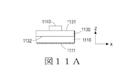
図11A〜11Fは、硬化された構造的塗膜を組み入れた様々な構成を示している。図11A〜11Fの各図は、可撓性基板1130の幅(x方向)に沿った断面を示す図である。図11Aにおいて、LED1140は可撓性基板1130の主要表面1131に配置され、硬化された構造的塗膜1110は可撓性基板1130の対向する主要表面1132に配置されている。必要に応じて、硬化された構造的塗膜の表面1111はテクスチャ処理され、前述したように、光および/または熱拡散に対して増大した有効表面積を提供することができる。
FIGS. 11A-11F illustrate various configurations incorporating a cured structural coating. Each of FIGS. 11A to 11F is a view showing a cross section along the width (x direction) of the
図11Bは、硬化された構造的塗膜1150がLED1140と同じ可撓性基板1131の同一面1131上に配置されている構成を示している。必要に応じて、硬化された構造的塗膜の表面1151はテクスチャ処理される。
FIG. 11B shows a configuration in which the cured
いくつかの構成において、構造的塗膜は可撓性基板の一以上のエッジに塗布される。これらの構成において、構造的塗膜は、表面積の大部分(50%を上回る)または実質的に大部分(75%を上回る)を被覆するように可撓性基板の片面または両面に塗布することもできる。図11Cに示したいくつかの実施形態において、構造的塗膜1160は、可撓性基板1130のエッジ1133、1134を被覆し、第1および/または第2の主要表面1131、1132の25%未満を被覆する。
In some configurations, the structural coating is applied to one or more edges of the flexible substrate. In these configurations, the structural coating is applied to one or both sides of the flexible substrate to cover the majority (greater than 50%) or substantially the majority (greater than 75%) of the surface area. You can also. In some embodiments shown in FIG. 11C, the
図11D〜図11Fは、構造的塗膜1170、1180、1190がLEDアセンブリを完全に囲繞する構成を示している。図11Dにおいて、LED1140は可撓性基板1130の第1の主要表面1131上に配置されている。図11Eにおいて、LED1140は可撓性基板の両主要表面1131、1132に配置されている。図11Fは、x方向に沿って平坦でない可撓性基板1139の実施例を示している。LED1140は硬化された構造的塗膜1190によって囲繞されている可撓性基板1139上に配置されている。
11D-11F show a configuration in which the
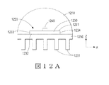
硬化された構造的塗膜は必要に応じて更なる塗膜および/または層と併用することができる。任意の層はLED電球へ熱的または光学的特性を付与することができる。任意の塗膜/層を含む構成のいくつかの実施例が図12Aおよび12Bに提供されているが、当業者は、本開示を読み解くうちに、多くの他の構成が適用可能であることを理解するであろう。図12Aは、可撓性基板1230の第1の主要表面1231上に配置されたLED1240を含むLEDアセンブリ1220を示している。硬化された構造的塗膜1210は、LED1240、第1の主要表面1231、および可撓性基板1230のエッジ1233、1234を被覆し、LEDアセンブリ1220を所定の形状に維持する。熱管理層1250、例えば、フィン状ヒートシンク機能などのヒートシンク機能1251を含む放熱層は可撓性基板1230の第2の主要表面に沿って配置されている。
The cured structural coating can be used in combination with further coatings and / or layers as required. Any layer can impart thermal or optical properties to the LED bulb. Although several examples of configurations including optional coatings / layers are provided in FIGS. 12A and 12B, those skilled in the art will appreciate that many other configurations are applicable while reading this disclosure. You will understand. FIG. 12A shows an
図12Bは、構造的塗膜1260の他に任意の光塗膜1270を使用することを示している。この特定の実施例において、硬化された構造的塗膜1260は、可撓性基板1230の一つの主要表面1232に配置され、(例えば、前述したように、光散乱、光拡散、光反射、光導波などを提供する)光塗膜1270は、一つの主要表面1232に対向する主要表面1231上に配置される。
FIG. 12B shows the use of an
構造的塗膜自体または構造的塗膜に追加して使用される光塗膜は先に図9Aに示した構成に類似している光導波を提供するために使用することができることに注目されたい。構造的塗膜がLEDアセンブリを所定形状に維持するために使用される場合、構造的支持体910は必要とされない。構造的塗膜は光シートと共に使用され、図9Bに示した構成に類似した構成の光導波を提供することができる。ここでもまた、構造的塗膜が所定の形状を維持する構成においても、構造的支持は必要とされない。構造的塗膜は、図9Cおよび図9Dの各図で示した線形プリズムおよびレンズ構造などの様々な光学特性を提供するために形成されるかまたは処理することができる。
Note that the structural coating itself or a light coating used in addition to the structural coating can be used to provide an optical waveguide similar to the configuration shown previously in FIG. 9A. . If a structural coating is used to keep the LED assembly in shape, the
本明細書に開示されているシステム、デバイス、または方法は、本明細書に記載されている特徴、構造、方法の一以上またはそれらの組合せを含むことができる。例えば、装置または方法は本明細書中に記載されている特徴および/またはプロセスの一以上を含むようにインプリメントすることができる。このようなデバイスまたは方法は本明細書に記載されている特性および/またはプロセスの全てを含む必要はないが、有用な構造および/または機能を提供する選択された特性および/またはプロセスを含むようにインプリメントすることができることを意図する。 A system, device, or method disclosed herein can include one or more of the features, structures, methods, or combinations thereof described herein. For example, an apparatus or method can be implemented to include one or more of the features and / or processes described herein. Such devices or methods need not include all of the features and / or processes described herein, but include selected features and / or processes that provide useful structure and / or function. It is intended that it can be implemented.
「発明を実施するための形態」において、以上記載した様々な態様のインプリメンテーションに対して数値および範囲が提供されている。これらの数値や範囲は例示目的のためにのみ提供され、本発明の特許請求の範囲を限定することを意図していない。例えば、本発明に記載されている実施形態は開示されている数値範囲を通して実施することが可能である。さらに、数多くの材料が様々な局面のインプリメンテーションにとって適切であると認識されている。これらの材料はあくまでも例示目的のために提供されており、特許請求の範囲を限定することを意図していない。 In the detailed description, numerical values and ranges are provided for implementations of the various aspects described above. These numbers and ranges are provided for illustrative purposes only and are not intended to limit the scope of the claims of the present invention. For example, the embodiments described in the present invention can be implemented through the disclosed numerical ranges. In addition, a number of materials have been recognized as suitable for various aspects of implementation. These materials are provided for illustrative purposes only and are not intended to limit the scope of the claims.
Claims (10)
口金と、
前記口金に連結されるとともに発光面と開放容積に対して外形を画定する形状に形成される少なくとも一の支持構造と、
二以上の電気的に接続されたLEDを含む少なくとも一のLEDアセンブリであって、前記支持構造の長さに沿って前記支持構造に取り付けられるとともに物理的接触することにて前記発光面を形成し、前記支持構造が前記LEDアセンブリの互いに隣接しているセグメント間に開口を有している、LEDアセンブリと、
を含むLED電球。 A light emitting diode (LED) bulb,
With a base,
At least one support structure connected to the base and formed in a shape defining an outer shape with respect to the light emitting surface and the open volume;
At least one LED assembly including two or more electrically connected LEDs, wherein the light emitting surface is formed by being attached to and in physical contact with the support structure along a length of the support structure. An LED assembly, wherein the support structure has an opening between adjacent segments of the LED assembly;
LED bulb including
支持構造を所定の形状に形成するステップであって、前記支持形状が発光面と開放容積に対して外形を画定するステップと、
前記長尺の支持構造へ少なくとも一のLEDアセンブリを取り付けるステップであって、前記LEDアセンブリが基板と前記基板に沿って互いに離間されている複数の電気的接続されたLEDを含むステップと、
を含む方法。 A method of making a light emitting diode (LED) bulb,
Forming a support structure in a predetermined shape, wherein the support shape defines an outer shape with respect to the light emitting surface and an open volume;
Attaching at least one LED assembly to the elongate support structure, the LED assembly including a substrate and a plurality of electrically connected LEDs spaced from each other along the substrate;
Including methods.
Applications Claiming Priority (2)
| Application Number | Priority Date | Filing Date | Title |
|---|---|---|---|
| US13/802,315 | 2013-03-13 | ||
| US13/802,315 US9353932B2 (en) | 2013-03-13 | 2013-03-13 | LED light bulb with structural support |
Publications (2)
| Publication Number | Publication Date |
|---|---|
| JP2014179318A true JP2014179318A (en) | 2014-09-25 |
| JP2014179318A5 JP2014179318A5 (en) | 2017-03-30 |
Family
ID=50396854
Family Applications (1)
| Application Number | Title | Priority Date | Filing Date |
|---|---|---|---|
| JP2014037120A Pending JP2014179318A (en) | 2013-03-13 | 2014-02-27 | Led light bulb with structural support |
Country Status (4)
| Country | Link |
|---|---|
| US (1) | US9353932B2 (en) |
| EP (1) | EP2778502B1 (en) |
| JP (1) | JP2014179318A (en) |
| CN (1) | CN104048195B (en) |
Cited By (3)
| Publication number | Priority date | Publication date | Assignee | Title |
|---|---|---|---|---|
| JP2016201206A (en) * | 2015-04-08 | 2016-12-01 | 三菱電機株式会社 | lamp |
| JP2020513587A (en) * | 2016-12-01 | 2020-05-14 | シグニファイ ホールディング ビー ヴィSignify Holding B.V. | Optical components for generating light effects |
| JP2022532452A (en) * | 2019-08-01 | 2022-07-14 | シグニファイ ホールディング ビー ヴィ | Optical structure for producing decorative lighting effects |
Families Citing this family (19)
| Publication number | Priority date | Publication date | Assignee | Title |
|---|---|---|---|---|
| US20230112968A1 (en) * | 2007-10-06 | 2023-04-13 | Lynk Labs, Inc. | High frequency multi-voltage and multi-brightness led lighting devices |
| US8764247B2 (en) * | 2012-11-07 | 2014-07-01 | Palo Alto Research Center Incorporated | LED bulb with integrated thermal and optical diffuser |
| US9528689B2 (en) | 2013-03-13 | 2016-12-27 | Palo Alto Research Center Incorporated | LED lighting device with cured structural support |
| WO2015081804A1 (en) * | 2013-12-02 | 2015-06-11 | 张晓峰 | Spiral led filament and light bulb using spiral led filament |
| US10060584B2 (en) * | 2014-09-11 | 2018-08-28 | City Electric Supply, Inc. | LED luminaire |
| US9523494B2 (en) * | 2015-02-17 | 2016-12-20 | Flextronics Ap, Llc | LED lighting unit |
| US9467190B1 (en) * | 2015-04-23 | 2016-10-11 | Connor Sport Court International, Llc | Mobile electronic device covering |
| JP6611036B2 (en) * | 2015-09-10 | 2019-11-27 | パナソニックIpマネジメント株式会社 | Light emitting device and light source for illumination |
| CN105588016B (en) * | 2016-03-11 | 2018-07-24 | 贵州光浦森光电有限公司 | A kind of LED filament light bulb with heat slinger |
| DE102016105537A1 (en) | 2016-03-24 | 2017-09-28 | Osram Opto Semiconductors Gmbh | FILAMENT WITH LIGHT-EMITTING SEMICONDUCTOR CHIPS, LAMPS AND METHOD FOR PRODUCING A FILAMENT |
| US10883694B2 (en) * | 2016-11-14 | 2021-01-05 | Lumileds Llc | Method of manufacturing an LED lighting assembly |
| US11212967B2 (en) * | 2017-01-20 | 2022-01-04 | Hgci, Inc. | Light emitting structures |
| DE102017109836B4 (en) | 2017-05-08 | 2023-07-06 | Ledvance Gmbh | Lamp with heat sink |
| US10989377B2 (en) * | 2017-09-14 | 2021-04-27 | Signify Holding B.V. | Lighting device and a method of manufacturing a lighting device |
| CN108397696A (en) * | 2018-04-28 | 2018-08-14 | 中国人民大学 | A kind of crystallo-luminescence high definition bulb lamp and production method |
| US10767816B1 (en) * | 2019-04-24 | 2020-09-08 | Xiamen Eco Lighting Co. Ltd. | Light bulb apparatus |
| CN113906253A (en) * | 2019-05-29 | 2022-01-07 | 昕诺飞控股有限公司 | Lighting device comprising a light-emitting filament |
| WO2022078813A1 (en) * | 2020-10-15 | 2022-04-21 | Signify Holding B.V. | A lighting device and a method of manufacturing a lighting device |
| US11906133B2 (en) | 2022-03-31 | 2024-02-20 | Alliance Sports Group, L.P. | Outdoor lighting apparatus |
Citations (6)
| Publication number | Priority date | Publication date | Assignee | Title |
|---|---|---|---|---|
| US20050207152A1 (en) * | 2004-03-18 | 2005-09-22 | Lighting Sciences, Inc. | Lighting element using electronically activated light emitting elements and method of making same |
| JP2007266246A (en) * | 2006-03-28 | 2007-10-11 | Mitsubishi Electric Corp | Led module |
| JP2011126262A (en) * | 2009-04-09 | 2011-06-30 | Teijin Ltd | Thermal conductive resin composite molded product and led illuminator |
| JP2012164659A (en) * | 2011-02-07 | 2012-08-30 | Nano Led Co Ltd | Led lamp having heat radiation and waterproof function |
| WO2012148384A1 (en) * | 2011-04-26 | 2012-11-01 | The Procter & Gamble Company | Stemmed lighting assembly with disk-shaped illumination element |
| JP2013033890A (en) * | 2011-08-03 | 2013-02-14 | Toyoda Gosei Co Ltd | Light emitting device |
Family Cites Families (28)
| Publication number | Priority date | Publication date | Assignee | Title |
|---|---|---|---|---|
| US6580228B1 (en) | 2000-08-22 | 2003-06-17 | Light Sciences Corporation | Flexible substrate mounted solid-state light sources for use in line current lamp sockets |
| US6578986B2 (en) * | 2001-06-29 | 2003-06-17 | Permlight Products, Inc. | Modular mounting arrangement and method for light emitting diodes |
| US6774566B2 (en) * | 2001-09-19 | 2004-08-10 | Toshiba Lighting & Technology Corporation | High pressure discharge lamp and luminaire |
| EP2298229A1 (en) | 2002-07-25 | 2011-03-23 | Jonathan S. Dahm | Method and apparatus for using light emitting diodes for curing |
| US7585096B2 (en) * | 2005-05-18 | 2009-09-08 | Visteon Global Technologies, Inc. | Compound trough reflector for LED light sources |
| US20110260945A1 (en) | 2007-08-03 | 2011-10-27 | Fumio Karasawa | Coating Composition and Article Using the Same |
| US20090140279A1 (en) * | 2007-12-03 | 2009-06-04 | Goldeneye, Inc. | Substrate-free light emitting diode chip |
| US7923272B2 (en) | 2007-12-28 | 2011-04-12 | Hwang-Pao Lee | Method of forming a resin cover lens of LED assembly |
| GB0801509D0 (en) | 2008-01-28 | 2008-03-05 | Photonstar Led Ltd | Light emitting system with optically transparent thermally conductive element |
| KR100978208B1 (en) | 2008-03-10 | 2010-08-25 | 민병현 | Built-up type LED lighting Device |
| KR100883344B1 (en) * | 2008-08-08 | 2009-02-12 | 김현민 | Light emmiting diode illuminating lamp |
| KR101324077B1 (en) | 2008-08-26 | 2013-10-31 | 딩구오 판 | A led multi-chip bonding die and a light stripe holding the bonding die |
| JP2010218714A (en) | 2009-03-13 | 2010-09-30 | Makoto Ishihara | Spiral led light-emitting object and led luminaire using it |
| TWM376709U (en) | 2009-09-02 | 2010-03-21 | Liquidleds Lighting Corp | Curved tubular LED lamp |
| WO2011088190A2 (en) | 2010-01-15 | 2011-07-21 | Edward Lawrence Sinofsky | Lightweight solid state lighting panel |
| US8783915B2 (en) | 2010-02-11 | 2014-07-22 | Bridgelux, Inc. | Surface-textured encapsulations for use with light emitting diodes |
| CN102782391B (en) | 2010-02-12 | 2016-08-03 | 科锐公司 | Solid state illumination device and assembly method thereof |
| FR2957723A1 (en) * | 2010-03-16 | 2011-09-23 | Design4 | System for supplying power of lighting device i.e. bulb, to LED, has receiving body electrically connected to voltage adapter to supply power to lighting device received with operating voltage of LED |
| JP5284308B2 (en) | 2010-04-19 | 2013-09-11 | 日本メクトロン株式会社 | Flexible circuit board and manufacturing method thereof |
| JP5486431B2 (en) | 2010-07-27 | 2014-05-07 | 日東電工株式会社 | LIGHT EMITTING DEVICE COMPONENT, LIGHT EMITTING DEVICE, AND ITS MANUFACTURING METHOD |
| CN201757351U (en) * | 2010-08-23 | 2011-03-09 | 高唐县高立电器设备厂 | Novel high-pole solar-energy combination type lighting lamp |
| JP5671356B2 (en) * | 2011-01-26 | 2015-02-18 | ローム株式会社 | LED bulb |
| US8314566B2 (en) * | 2011-02-22 | 2012-11-20 | Quarkstar Llc | Solid state lamp using light emitting strips |
| US20120243212A1 (en) | 2011-03-22 | 2012-09-27 | David Smith | Portable and bendable utility light |
| US20130010463A1 (en) * | 2011-07-05 | 2013-01-10 | Industrial Technology Research Institute | Illumination device |
| CN202769319U (en) * | 2012-06-06 | 2013-03-06 | 深圳市众明半导体照明有限公司 | LED bulb |
| CN102889480B (en) * | 2012-07-19 | 2016-11-23 | 王定锋 | The LED bulb module of three-dimensional light and manufacture method |
| US9528689B2 (en) * | 2013-03-13 | 2016-12-27 | Palo Alto Research Center Incorporated | LED lighting device with cured structural support |
-
2013
- 2013-03-13 US US13/802,315 patent/US9353932B2/en not_active Expired - Fee Related
-
2014
- 2014-02-27 JP JP2014037120A patent/JP2014179318A/en active Pending
- 2014-02-28 CN CN201410072125.5A patent/CN104048195B/en not_active Expired - Fee Related
- 2014-03-11 EP EP14158751.9A patent/EP2778502B1/en not_active Not-in-force
Patent Citations (6)
| Publication number | Priority date | Publication date | Assignee | Title |
|---|---|---|---|---|
| US20050207152A1 (en) * | 2004-03-18 | 2005-09-22 | Lighting Sciences, Inc. | Lighting element using electronically activated light emitting elements and method of making same |
| JP2007266246A (en) * | 2006-03-28 | 2007-10-11 | Mitsubishi Electric Corp | Led module |
| JP2011126262A (en) * | 2009-04-09 | 2011-06-30 | Teijin Ltd | Thermal conductive resin composite molded product and led illuminator |
| JP2012164659A (en) * | 2011-02-07 | 2012-08-30 | Nano Led Co Ltd | Led lamp having heat radiation and waterproof function |
| WO2012148384A1 (en) * | 2011-04-26 | 2012-11-01 | The Procter & Gamble Company | Stemmed lighting assembly with disk-shaped illumination element |
| JP2013033890A (en) * | 2011-08-03 | 2013-02-14 | Toyoda Gosei Co Ltd | Light emitting device |
Cited By (6)
| Publication number | Priority date | Publication date | Assignee | Title |
|---|---|---|---|---|
| JP2016201206A (en) * | 2015-04-08 | 2016-12-01 | 三菱電機株式会社 | lamp |
| JP2020513587A (en) * | 2016-12-01 | 2020-05-14 | シグニファイ ホールディング ビー ヴィSignify Holding B.V. | Optical components for generating light effects |
| JP7086071B2 (en) | 2016-12-01 | 2022-06-17 | シグニファイ ホールディング ビー ヴィ | Optical components for producing light effects |
| JP2022532452A (en) * | 2019-08-01 | 2022-07-14 | シグニファイ ホールディング ビー ヴィ | Optical structure for producing decorative lighting effects |
| JP7262660B2 (en) | 2019-08-01 | 2023-04-21 | シグニファイ ホールディング ビー ヴィ | Optical structures for producing decorative lighting effects |
| US11754230B2 (en) | 2019-08-01 | 2023-09-12 | Signify Holding B.V. | Optical structure for producing decorative lighting effects |
Also Published As
| Publication number | Publication date |
|---|---|
| EP2778502A3 (en) | 2015-09-02 |
| US20140268739A1 (en) | 2014-09-18 |
| US9353932B2 (en) | 2016-05-31 |
| CN104048195B (en) | 2018-11-30 |
| EP2778502B1 (en) | 2017-05-10 |
| CN104048195A (en) | 2014-09-17 |
| EP2778502A2 (en) | 2014-09-17 |
Similar Documents
| Publication | Publication Date | Title |
|---|---|---|
| JP6158728B2 (en) | LED illuminator having a cured structural support | |
| JP2014179318A (en) | Led light bulb with structural support | |
| US20190353327A1 (en) | Light-Emitting Device with Total Internal Reflection (TIR) Extractor | |
| KR101809185B1 (en) | Lightweight heat sinks and led lamps employing same | |
| US9091420B2 (en) | Illumination apparatus | |
| US9230943B2 (en) | Solid state illumination device | |
| TWI553271B (en) | Solid state light with optical guide and integrated thermal guide | |
| US8963405B2 (en) | Light bulb with thermal features | |
| US20060146531A1 (en) | Linear lighting apparatus with improved heat dissipation | |
| US20110305024A1 (en) | Led tube lamp | |
| US20110205738A1 (en) | Troffer-style light fixture with cross-lighting | |
| JP6173476B2 (en) | Lighting device including an improved heat transfer device | |
| US20100020543A1 (en) | Led lighting device with light-conducting member | |
| CN111911820B (en) | LED lighting equipment | |
| EP3044626B1 (en) | Light-emitting device with total internal reflection (tir) extractor | |
| CN107850272B (en) | Lighting device with light guide | |
| TWI401396B (en) | Led fluorescent lamp |
Legal Events
| Date | Code | Title | Description |
|---|---|---|---|
| A521 | Request for written amendment filed |
Free format text: JAPANESE INTERMEDIATE CODE: A523 Effective date: 20170224 |
|
| A621 | Written request for application examination |
Free format text: JAPANESE INTERMEDIATE CODE: A621 Effective date: 20170224 |
|
| A871 | Explanation of circumstances concerning accelerated examination |
Free format text: JAPANESE INTERMEDIATE CODE: A871 Effective date: 20170224 |
|
| A975 | Report on accelerated examination |
Free format text: JAPANESE INTERMEDIATE CODE: A971005 Effective date: 20170427 |
|
| A131 | Notification of reasons for refusal |
Free format text: JAPANESE INTERMEDIATE CODE: A131 Effective date: 20170509 |
|
| A521 | Request for written amendment filed |
Free format text: JAPANESE INTERMEDIATE CODE: A523 Effective date: 20170808 |
|
| A02 | Decision of refusal |
Free format text: JAPANESE INTERMEDIATE CODE: A02 Effective date: 20171003 |