JP2014178172A - Infrared sensor and manufacturing method thereof - Google Patents
Infrared sensor and manufacturing method thereof Download PDFInfo
- Publication number
- JP2014178172A JP2014178172A JP2013051506A JP2013051506A JP2014178172A JP 2014178172 A JP2014178172 A JP 2014178172A JP 2013051506 A JP2013051506 A JP 2013051506A JP 2013051506 A JP2013051506 A JP 2013051506A JP 2014178172 A JP2014178172 A JP 2014178172A
- Authority
- JP
- Japan
- Prior art keywords
- region
- sensor
- forming
- thermopile
- layer
- Prior art date
- Legal status (The legal status is an assumption and is not a legal conclusion. Google has not performed a legal analysis and makes no representation as to the accuracy of the status listed.)
- Pending
Links
- 238000004519 manufacturing process Methods 0.000 title claims abstract description 31
- 239000000758 substrate Substances 0.000 claims abstract description 40
- 239000004065 semiconductor Substances 0.000 claims abstract description 31
- 238000005530 etching Methods 0.000 claims abstract description 30
- 230000002093 peripheral effect Effects 0.000 claims abstract description 27
- 238000000034 method Methods 0.000 claims description 37
- 230000015572 biosynthetic process Effects 0.000 abstract description 5
- 229910021420 polycrystalline silicon Inorganic materials 0.000 description 26
- 229920005591 polysilicon Polymers 0.000 description 26
- 230000008569 process Effects 0.000 description 25
- VYPSYNLAJGMNEJ-UHFFFAOYSA-N Silicium dioxide Chemical compound O=[Si]=O VYPSYNLAJGMNEJ-UHFFFAOYSA-N 0.000 description 14
- 229910052814 silicon oxide Inorganic materials 0.000 description 14
- 238000004088 simulation Methods 0.000 description 9
- BOTDANWDWHJENH-UHFFFAOYSA-N Tetraethyl orthosilicate Chemical compound CCO[Si](OCC)(OCC)OCC BOTDANWDWHJENH-UHFFFAOYSA-N 0.000 description 7
- 238000010521 absorption reaction Methods 0.000 description 7
- 230000008859 change Effects 0.000 description 7
- 229910004298 SiO 2 Inorganic materials 0.000 description 6
- XUIMIQQOPSSXEZ-UHFFFAOYSA-N Silicon Chemical compound [Si] XUIMIQQOPSSXEZ-UHFFFAOYSA-N 0.000 description 6
- 229910052782 aluminium Inorganic materials 0.000 description 6
- XAGFODPZIPBFFR-UHFFFAOYSA-N aluminium Chemical compound [Al] XAGFODPZIPBFFR-UHFFFAOYSA-N 0.000 description 6
- 229910052710 silicon Inorganic materials 0.000 description 6
- 239000010703 silicon Substances 0.000 description 6
- 229910052751 metal Inorganic materials 0.000 description 4
- 239000002184 metal Substances 0.000 description 4
- WGTYBPLFGIVFAS-UHFFFAOYSA-M tetramethylammonium hydroxide Chemical compound [OH-].C[N+](C)(C)C WGTYBPLFGIVFAS-UHFFFAOYSA-M 0.000 description 4
- 239000003566 sealing material Substances 0.000 description 3
- 230000009471 action Effects 0.000 description 2
- 238000009792 diffusion process Methods 0.000 description 2
- 230000000694 effects Effects 0.000 description 2
- 238000010438 heat treatment Methods 0.000 description 2
- 239000000243 solution Substances 0.000 description 2
- RYGMFSIKBFXOCR-UHFFFAOYSA-N Copper Chemical compound [Cu] RYGMFSIKBFXOCR-UHFFFAOYSA-N 0.000 description 1
- ATJFFYVFTNAWJD-UHFFFAOYSA-N Tin Chemical compound [Sn] ATJFFYVFTNAWJD-UHFFFAOYSA-N 0.000 description 1
- MXSJNBRAMXILSE-UHFFFAOYSA-N [Si].[P].[B] Chemical compound [Si].[P].[B] MXSJNBRAMXILSE-UHFFFAOYSA-N 0.000 description 1
- 239000003513 alkali Substances 0.000 description 1
- 239000012670 alkaline solution Substances 0.000 description 1
- 238000000137 annealing Methods 0.000 description 1
- 239000003990 capacitor Substances 0.000 description 1
- 229910052802 copper Inorganic materials 0.000 description 1
- 239000010949 copper Substances 0.000 description 1
- 238000001514 detection method Methods 0.000 description 1
- 230000004907 flux Effects 0.000 description 1
- 239000011521 glass Substances 0.000 description 1
- 239000012535 impurity Substances 0.000 description 1
- 150000002500 ions Chemical class 0.000 description 1
- 238000002955 isolation Methods 0.000 description 1
- 238000001459 lithography Methods 0.000 description 1
- 239000011159 matrix material Substances 0.000 description 1
- 238000005259 measurement Methods 0.000 description 1
- 239000012528 membrane Substances 0.000 description 1
- 230000004048 modification Effects 0.000 description 1
- 238000012986 modification Methods 0.000 description 1
- 230000003647 oxidation Effects 0.000 description 1
- 238000007254 oxidation reaction Methods 0.000 description 1
- 238000005498 polishing Methods 0.000 description 1
- 230000001681 protective effect Effects 0.000 description 1
- 230000009467 reduction Effects 0.000 description 1
- 230000004044 response Effects 0.000 description 1
- 230000035945 sensitivity Effects 0.000 description 1
- 239000000126 substance Substances 0.000 description 1
- 230000008685 targeting Effects 0.000 description 1
- 230000007704 transition Effects 0.000 description 1
Images


Classifications
-
- G—PHYSICS
- G01—MEASURING; TESTING
- G01J—MEASUREMENT OF INTENSITY, VELOCITY, SPECTRAL CONTENT, POLARISATION, PHASE OR PULSE CHARACTERISTICS OF INFRARED, VISIBLE OR ULTRAVIOLET LIGHT; COLORIMETRY; RADIATION PYROMETRY
- G01J5/00—Radiation pyrometry, e.g. infrared or optical thermometry
- G01J5/10—Radiation pyrometry, e.g. infrared or optical thermometry using electric radiation detectors
- G01J5/12—Radiation pyrometry, e.g. infrared or optical thermometry using electric radiation detectors using thermoelectric elements, e.g. thermocouples
-
- G—PHYSICS
- G01—MEASURING; TESTING
- G01J—MEASUREMENT OF INTENSITY, VELOCITY, SPECTRAL CONTENT, POLARISATION, PHASE OR PULSE CHARACTERISTICS OF INFRARED, VISIBLE OR ULTRAVIOLET LIGHT; COLORIMETRY; RADIATION PYROMETRY
- G01J5/00—Radiation pyrometry, e.g. infrared or optical thermometry
- G01J5/02—Constructional details
- G01J5/0225—Shape of the cavity itself or of elements contained in or suspended over the cavity
- G01J5/024—Special manufacturing steps or sacrificial layers or layer structures
Abstract
Description
本発明は、赤外線センサおよびその製造方法に関するものである。 The present invention relates to an infrared sensor and a method for manufacturing the same.
近年の電子機器においては、周囲環境を検出し、その検出結果を運転制御に利用することが行なわれている。たとえばエアコンにおいては、人の存在を検知し、人の存在する場所を狙って温度制御するといった運転制御が行なわれている。また、照明機器においては、一定領域内における人の存在を検知して、当該領域の照明をオンにするといった制御が行なわれている。このような制御においては、周囲環境を検出するためのセンサ装置が用いられ、センサ装置の一種として、物体からの輻射熱によって非接触で物体温度を検知する赤外線センサが用いられる。 In recent electronic devices, the surrounding environment is detected, and the detection result is used for operation control. For example, in an air conditioner, operation control is performed in which the presence of a person is detected and temperature control is performed targeting a place where the person is present. Further, in the lighting device, control is performed such that the presence of a person in a certain area is detected and lighting in the area is turned on. In such control, a sensor device for detecting the surrounding environment is used, and an infrared sensor that detects an object temperature in a non-contact manner by radiant heat from the object is used as a kind of sensor device.
従来技術に基づく赤外線センサの一例が、特許第4661207号(特許文献1)に記載されている。特許文献1に記載された赤外線センサは、基板に設けられた凹部の上方で浮くように配置された正方形の赤外線吸収膜を備えている。赤外線吸収膜は、2本の支持梁によって支持されている。基板の上側にシリコン酸化膜が積層されており、支持梁は赤外線吸収膜をシリコン酸化膜に接続している。各支持梁は2度直角に折れ曲がった形状をしており、各支持梁の内部にはP型ポリシリコン層およびN型ポリシリコン層が線状に形成されており、これらはサーモパイルを構成している。赤外線吸収膜が赤外線を受けて高温となることで、赤外線吸収膜と周辺のシリコン酸化膜との間に温度差が生じ、この温度差をサーモパイルによって電気信号に変換することによって、赤外線の量を検出することができる。
An example of an infrared sensor based on the prior art is described in Japanese Patent No. 4661207 (Patent Document 1). The infrared sensor described in
特許文献1では、赤外線センサを得るために、以下のような製造方法が記載されている。まず、シリコン基板においてLOCOSによりセンサ領域と配線領域とに素子分離を行なう。センサ領域にポリシリコンからなるエッチング犠牲層を形成し、配線領域においてポリシリコンからなるゲート配線を形成する。センサ領域においてさらにポリシリコンからなるエッチング犠牲層を積層することによってセンサ領域の高さを底上げする。全面を覆うようにシリコン酸化膜を形成する。センサ領域においてP型ポリシリコン層、N型ポリシリコン層を所定形状に形成してサーモパイルを形成する。
In
センサ領域および配線領域において所定のアルミ配線を形成し、これらのアルミ配線を覆うように全面にシリコン酸化膜を形成する。シリコン酸化膜の表面をCMPなどによりアルミ配線が露出しない程度に薄くして平坦化する。センサ領域においてシリコン酸化膜を選択的にエッチングしてスリットを形成する。スリットを通じて強アルカリ溶液を用いて異方性エッチングを行なうことによって、センサ領域のエッチング犠牲層およびシリコン基板を除去する。その結果、センサ領域においては、シリコン基板の上面から掘り下げた形の空洞が形成される。これにより、サーモパイルを含む部材がシリコン基板から浮いた構造が得られる。 A predetermined aluminum wiring is formed in the sensor region and the wiring region, and a silicon oxide film is formed on the entire surface so as to cover these aluminum wirings. The surface of the silicon oxide film is flattened by CMP or the like so that the aluminum wiring is not exposed. In the sensor region, the silicon oxide film is selectively etched to form a slit. By performing anisotropic etching using a strong alkali solution through the slit, the etching sacrificial layer and the silicon substrate in the sensor region are removed. As a result, in the sensor region, a cavity that is dug from the upper surface of the silicon substrate is formed. Thereby, the structure where the member containing a thermopile floated from the silicon substrate is obtained.
特許文献1に記載された赤外線センサの製造方法では、配線領域の配線を形成した後でセンサ領域のサーモパイルを形成している。センサ領域のサーモパイルを形成する工程にはイオン拡散工程が含まれ、イオン拡散工程は加熱を伴う。この加熱により、既に配線が形成されている配線領域において拡散濃度が変化し、その結果、回路特性に変化が生じる。配線領域では、スイッチング回路や増幅回路など、さまざまな回路素子が形成されるが、このように回路素子形成より後の工程で加わる熱によって特性に変化が生じるような製造方法である場合、回路を変更するごとに設計段階での調整が必要になったり、他の製品に比べて回路設計を特別に変更する必要が生じたりする。
In the manufacturing method of the infrared sensor described in
また、配線領域における配線形成のための積層数が増加した場合、または、センサを薄型化すべき場合には、センサ領域の底上げすべき高さが増すので、センサ領域に形成するエッチング犠牲層の厚みを増加させる必要がある。エッチング犠牲層をシリコン酸化膜によって形成する場合、1回の成長工程によって得られる厚みは限りがあるので、大きな厚みのエッチング犠牲層を得るためには、膜の成長工程を複数回繰り返さなければならず、工程数が増大してしまう。また、その場合、回路配線のリソグラフィ時にマスクと基板との間にギャップが生じるので、パターンサイズにばらつきが生じる。この影響により、回路素子の導通不良が生じるおそれがある。 Further, when the number of stacked layers for wiring formation in the wiring region increases or when the sensor is to be thinned, the height of the sensor region to be raised increases, so the thickness of the etching sacrificial layer formed in the sensor region Need to be increased. When the etching sacrificial layer is formed of a silicon oxide film, the thickness that can be obtained by one growth process is limited. Therefore, in order to obtain an etching sacrificial layer having a large thickness, the film growth process must be repeated a plurality of times. However, the number of processes increases. In this case, a gap is generated between the mask and the substrate during circuit wiring lithography, resulting in variations in pattern size. Due to this influence, there is a possibility that a conduction failure of the circuit element occurs.
そこで、本発明は、センサ領域のサーモパイルを形成する際の熱によって、周辺回路領域において回路特性が変化するという現象に伴う不都合を回避した赤外線センサおよびその製造方法を提供することを目的とする。 SUMMARY OF THE INVENTION An object of the present invention is to provide an infrared sensor and a method for manufacturing the infrared sensor that avoids the inconvenience associated with a phenomenon in which circuit characteristics change in a peripheral circuit region due to heat when forming a thermopile in the sensor region.
上記目的を達成するため、本発明に基づく赤外線センサの製造方法は、センサ領域となるべき第1領域および周辺回路領域となるべき第2領域を上面に有する半導体基板の上記第1領域にサーモパイル支持層を形成する工程と、上記サーモパイル支持層の上面にサーモパイルを形成する工程と、上記サーモパイルを形成する工程より後で、上記第2領域に回路素子を形成する工程と、上記第1領域および上記第2領域を覆って上部層を形成する工程と、上記第1領域において上記上部層を途中まで掘り下げる工程と、上記上部層を途中まで掘り下げた領域のうち一部の領域において上記上部層をさらに掘り下げることによって上記半導体基板が露出するエッチングホールを形成する工程と、上記エッチングホールを通じて上記第1領域にある上記半導体基板の一部をエッチングして上記サーモパイル支持層および上記サーモパイルを上記半導体基板から浮かせることによって、センサ部を形成する工程とを含み、上記センサ部の上面は、上記第2領域における上記上部層の上面より低い位置となっている。 In order to achieve the above object, an infrared sensor manufacturing method according to the present invention provides a thermopile support on the first region of a semiconductor substrate having a first region to be a sensor region and a second region to be a peripheral circuit region on the upper surface. A step of forming a layer; a step of forming a thermopile on an upper surface of the thermopile support layer; a step of forming a circuit element in the second region after the step of forming the thermopile; A step of forming an upper layer covering the second region; a step of digging the upper layer partway in the first region; and a part of the region in which the upper layer is dug partway. Forming an etching hole in which the semiconductor substrate is exposed by digging, and being in the first region through the etching hole Forming a sensor part by etching a part of the semiconductor substrate to float the thermopile support layer and the thermopile from the semiconductor substrate, and the upper surface of the sensor part is the upper part in the second region. The position is lower than the upper surface of the layer.
本発明によれば、センサ領域となるべき第1領域にサーモパイルを早い段階で形成した後で、第2領域に回路素子を形成し、その上の上部層を一旦形成してからセンサ領域において凹部を掘り下げることによって、サーモパイルに近い層まで露出させてサーモパイルを含むセンサ部を形成することとしているので、周辺回路領域における回路素子を形成した後は、サーモパイル形成の工程に伴う熱が加わることを避けることができる。したがって、センサ領域のサーモパイルを形成する際の熱によって、周辺回路領域において回路特性が変化するという現象に伴う不都合を回避しつつ赤外線センサを製造することができる。 According to the present invention, after the thermopile is formed in the first region to be the sensor region at an early stage, the circuit element is formed in the second region, the upper layer is once formed thereon, and then the recess is formed in the sensor region. The sensor part including the thermopile is formed by exposing the layer close to the thermopile by digging in, so after the circuit elements in the peripheral circuit region are formed, avoid the heat associated with the thermopile forming process. be able to. Therefore, it is possible to manufacture an infrared sensor while avoiding the disadvantage associated with the phenomenon that the circuit characteristics change in the peripheral circuit region due to heat when forming the thermopile in the sensor region.
(実施の形態1)
(製造方法)
図1〜図10を参照して、本発明に基づく実施の形態1における赤外線センサの製造方法について説明する。本実施の形態における赤外線センサの製造方法のフローチャートを図1に示す。
(Embodiment 1)
(Production method)
With reference to FIGS. 1-10, the manufacturing method of the infrared sensor in
本実施の形態における赤外線センサの製造方法は、センサ領域となるべき第1領域および周辺回路領域となるべき第2領域を上面に有する半導体基板の前記第1領域にサーモパイル支持層を形成する工程S1と、前記サーモパイル支持層の上面にサーモパイルを形成する工程S2と、前記サーモパイルを形成する工程S2より後で、前記第2領域に回路素子を形成する工程S3と、前記第1領域および前記第2領域を覆って上部層を形成する工程S4と、前記第1領域において前記上部層を途中まで掘り下げる工程S5と、前記上部層を途中まで掘り下げた領域のうち一部の領域において前記上部層をさらに掘り下げることによって前記半導体基板が露出するエッチングホールを形成する工程S6と、前記エッチングホールを通じて前記第1領域にある前記半導体基板の一部をエッチングして前記サーモパイル支持層および前記サーモパイルを前記半導体基板から浮かせることによって、センサ部を形成する工程S7とを含み、前記センサ部の上面は、前記第2領域における前記上部層の上面より低い位置となっている。 In the manufacturing method of the infrared sensor in the present embodiment, the thermopile support layer is formed in the first region of the semiconductor substrate having the first region to be the sensor region and the second region to be the peripheral circuit region on the upper surface. A step S2 of forming a thermopile on the upper surface of the thermopile support layer, a step S3 of forming a circuit element in the second region after the step S2 of forming the thermopile, the first region and the second region A step S4 for forming an upper layer covering the region; a step S5 for digging the upper layer partway in the first region; and a part of the region obtained by digging the upper layer partway. Step S6 of forming an etching hole exposing the semiconductor substrate by digging down, and the first through the etching hole. Forming a sensor part by etching a part of the semiconductor substrate in the region to float the thermopile support layer and the thermopile from the semiconductor substrate, and the upper surface of the sensor part includes the second surface The position is lower than the upper surface of the upper layer in the region.
半導体基板とは、たとえばシリコン基板である。回路素子とは、たとえばトランジスタ、キャパシタ、抵抗体などである。 The semiconductor substrate is, for example, a silicon substrate. The circuit element is, for example, a transistor, a capacitor, a resistor, or the like.
以下に各工程を詳しく説明する。
まず、図2に示すように半導体基板1を用意する。ここでは、説明の便宜のため、センサ領域401と周辺回路領域402とに属する各要素を代表的に抽出して並べて表示している。センサ領域401として表示されている領域は第1領域に相当し、周辺回路領域402として表示されている領域は第2領域に相当する。
Each step will be described in detail below.
First, as shown in FIG. 2, a
図3に示すように半導体基板1の上面の一部にLOCOS(Local Oxidation of Silicon)法によりシリコン酸化膜21を形成する。シリコン酸化膜21のうちセンサ領域401にあるものはサーモパイル支持層に相当する。したがって、シリコン酸化膜21を形成する工程は、工程S1に相当する。
As shown in FIG. 3, a
図4に示すように、シリコン酸化膜21の上にSiN膜22を形成し、さらにその上を覆うようにSiO2膜23を形成する。SiO2膜23の上側を全体的に覆うようにポリシリコン膜を形成し、このポリシリコン膜をエッチングすることによって、のちにサーモパイルを構成する熱電対に相当する部分のみを残す。ポリシリコン膜にP型およびN型の不純物をそれぞれ局所的に注入し、アニール処理を行なうことによって、図4に示すようにP型ポリシリコン膜25およびN型ポリシリコン膜26を形成する。P型ポリシリコン膜25およびN型ポリシリコン膜26はサーモパイル24を構成する。このようにP型ポリシリコン膜25およびN型ポリシリコン膜26を形成する工程は、サーモパイルを形成する工程であるので工程S2に相当する。
As shown in FIG. 4, an
実際にはサーモパイルは複数の熱電対が接続された集合体として構成されるのが通常であり、サーモパイルに含まれる複数対のP型ポリシリコン膜25およびN型ポリシリコン膜26が配列されて形成される。図4では、説明の便宜のため、代表して1対の熱電対に相当する部分のP型ポリシリコン膜25およびN型ポリシリコン膜26のみを表示している。
Actually, the thermopile is usually configured as an assembly in which a plurality of thermocouples are connected, and a plurality of pairs of P-
工程S2より後で、図5に示すように、周辺回路領域402に回路素子としてトランジスタ28a,28bおよび抵抗体39を形成する。これらの回路素子を形成する工程は、工程S3に相当する。ただし、周辺回路領域402に形成される回路素子としてここで示したものはあくまで一例であって、回路素子の種類、数、配置はここで示したものに限らない。工程S3が行なわれるのは、工程S2によりサーモパイル24を形成した後であるので、工程S3で形成される回路素子は、サーモパイル形成時の熱の影響を受けない。
After step S2,
図6に示すように、絶縁層27を形成し、表面を平坦化し、絶縁層27の上面に配線層29aを形成する。絶縁層27は、たとえばBPSG(Boron Phosphorus Silicon Glass)層であってよい。表面の平坦化はたとえばCMP(Chemical Mechanical Polishing)法によって行なってよい。配線層29aはたとえばアルミニウムによって形成することができる。センサ領域401においては、配線層29aの一部は絶縁層27にあけられた貫通孔を介してP型ポリシリコン膜25またはN型ポリシリコン膜26に接続される。周辺回路領域402においては、配線層29aの一部は絶縁層27にあけられた貫通孔を介してトランジスタ28a,28bまたは抵抗体39に接続される。絶縁層27および配線層29aを覆うように絶縁層30をさらに形成し、絶縁層30の上面に配線層29bを形成する。配線層29bの一部は、絶縁層30の所定の位置にあけられた貫通孔を介して配線層29aのいずれかに接続される。配線層29bはたとえばアルミニウムによって形成することができる。配線層29a,29bは、たとえばアルミニウム層と銅層との積層体によって形成してもよい。周辺回路領域402においては、配線層29a,29bによって回路素子に関係する必要な配線がなされる。
As shown in FIG. 6, the insulating
図6に示すように、絶縁層30および配線層29bの全体を覆うようにSiO2膜31を形成する。SiO2膜31の上面を覆うようにさらにSiN膜32が形成される。SiO2膜31とSiN膜32とを合わせた部分は、配線保護膜40となる。
As shown in FIG. 6, an SiO 2 film 31 is formed so as to cover the entire insulating
ここで示した例では、絶縁層27からSiN膜32までが「上部層」41に相当する。したがって、絶縁層27を形成する工程からSiN膜32を形成する工程までが、工程S4に相当する。
In the example shown here, the layers from the insulating
図7に示すように、エッチングを行なうことによって、センサ領域401に凹部33を形成する。凹部33は、配線層29aよりやや高いところに底面が位置するように形成される。このエッチングの工程は、第1領域であるところのセンサ領域において上部層を途中まで掘り下げる工程であるので工程S5に相当する。
As shown in FIG. 7, the
工程S2においてサーモパイルを形成した後に、工程S3において回路素子を形成し、さらに工程S4において各種配線を含む上部層41を形成したことによって、サーモパイル24は一時は上部層41に深く埋もれた状態となっていたが、工程S5でセンサ領域401において上部層41を途中まで掘り下げたことによって、再びサーモパイル24は凹部33の底面の下に浅く埋もれただけの状態となる。このような状態にしてから、以下のようにセンサ部を作製するための工程を行なう。
After forming the thermopile in step S2, circuit elements are formed in step S3, and the
図8に示すように、凹部33の底面のうちセンサ部となるべき領域に吸収層34を形成する。吸収層34はTiまたはTiNによって形成することができる。さらに全体にわたって覆うようにTEOS膜35を形成する。これにより、凹部33の底面はTEOS膜35によって覆われる。吸収層34もTEOS膜35によって覆われる。
As shown in FIG. 8, an
さらに図8に示すように、適当な時点において、抵抗体39の上方で配線層29bが露出するように凹部36を形成しておく。のちに凹部36の内面を覆うように金属膜37を形成する。金属膜37はAu膜を含んでいてよい。
Further, as shown in FIG. 8, at an appropriate time, a
図9に示すように、凹部33の底面の一部において半導体基板1が直接露出するようにエッチングホール38を形成する。エッチングホール38はセンサ開口部内の一部の領域を占める。エッチングホール38を形成する工程は工程S6に相当する。
As shown in FIG. 9, an
図10に示すように、エッチングホール38を介して半導体基板1に対するエッチングを行なう。このエッチングには、アルカリ溶液を用いることができる。このエッチングには、たとえばTMAH(水酸化テトラメチルアンモニウム)溶液を用いることができる。このエッチングにより、半導体基板1の上面を掘り下げるように凹部5が形成される。この結果、半導体基板1から浮いて支持された構造のセンサ部2が形成される。センサ領域401内に複数のセンサ部2が配列される場合には、個々のセンサ部2に対応してそれぞれ凹部5が形成される。このように、半導体基板1に対するエッチングによりセンサ部2を形成する工程は、工程S7に相当する。
As shown in FIG. 10, the
なお、センサ部2は上部層31のいずれかの箇所から1本以上の梁によって支持されている。センサ部2の平面的形状としては、公知のサーモパイル型赤外線センサの平面的形状を採用してよい。センサ部2の平面的形状は、たとえば特許文献1に記載されているものであってもよい。
The
図10に示したように、センサ部2の上面2uは、第2領域としての周辺回路領域402における上部層41の上面41uより低い位置となっている。こうして、赤外線センサ101が得られる。
As shown in FIG. 10, the upper surface 2u of the
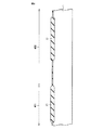
図11に示すように、封止材503を利用してキャップ部材502を貼り付ける。封止材503としては金属を用いることができる。キャップ部材502と基板1とに覆われた内部空間505は、公知技術によって真空に封止してもよい。センサ部2は内部空間505内に支持される。図10では、センサ部2は模式的に表示されているので、複数のセンサ部2が全て一体的に連続した板であるかのように見えるが、実際には、個々のセンサ部2が半導体基板1の凹部5の上方で浮くようにしてそれぞれ何らかの梁によって保持されている。図10では、説明の便宜のため、4個のセンサ部2のみを表示しているが、実際にはより多くの個数のセンサ部2が配列されていてよい。各凹部5内の空間は内部空間505に連通している。
As shown in FIG. 11, the
このようにして赤外線センサチップ601が得られる。赤外線センサチップ601は、複数のセンサ部2がマトリックス状に配列された受像領域を有する。赤外線センサチップ601には複数の赤外線センサ101が含まれる。
In this way, the
(作用・効果)
本実施の形態における赤外線センサの製造方法によれば、センサ領域にサーモパイルを早い段階で形成した後で周辺回路領域に回路素子を形成し、その上に配置される上部層までも含めて一旦形成してからセンサ領域において凹部を掘り下げることによってサーモパイルに近い層まで露出させ、その状態でサーモパイルを含むセンサ部を形成することとしているので、周辺回路領域における回路素子を形成した後は、サーモパイル形成の工程に伴う熱が加わることを避けることができる。したがって、センサ領域のサーモパイルを形成する際の熱によって、周辺回路領域において回路特性が変化するという現象に伴う不都合を回避しつつ赤外線センサを製造することができる。
(Action / Effect)
According to the manufacturing method of the infrared sensor in the present embodiment, after forming the thermopile in the sensor region at an early stage, the circuit elements are formed in the peripheral circuit region and once formed including the upper layer disposed thereon. Then, by digging the recess in the sensor area, the layer close to the thermopile is exposed and the sensor part including the thermopile is formed in that state, so after forming the circuit element in the peripheral circuit area, the thermopile formation Heat applied during the process can be avoided. Therefore, it is possible to manufacture an infrared sensor while avoiding the disadvantage associated with the phenomenon that the circuit characteristics change in the peripheral circuit region due to heat when forming the thermopile in the sensor region.
本実施の形態で示したように、サーモパイル支持層を形成する工程S1は、LOCOS法によって酸化膜を形成する工程を含むことが好ましい。この方法を採用することにより、適切なサーモパイル支持層を容易に形成することができる。 As shown in the present embodiment, the step S1 of forming the thermopile support layer preferably includes a step of forming an oxide film by the LOCOS method. By adopting this method, an appropriate thermopile support layer can be easily formed.
本実施の形態で示したように、上部層は、内部に配線層29a,29bを含むことが好ましい。この方法を採用することにより、回路素子間の接続に必要な配線を容易に確保することができる。
As shown in the present embodiment, the upper layer preferably includes
(実施の形態2)
(構成)
図11を参照して、本発明に基づく実施の形態2における赤外線センサ101について説明する。赤外線センサ101は、上面に凹部5を有する半導体基板1と、半導体基板1の上側に形成され、凹部5に対応した開口部であるセンサ開口部を有する上部層41と、前記センサ開口部の内周の少なくとも1ヶ所につながるように、凹部5の内面から離隔した状態で前記センサ開口部内に支持されるセンサ部2とを備える。センサ部2はサーモパイルを備える。平面的に見て前記センサ開口部とは異なる場所において、回路素子が上部層41の内部に形成されている周辺回路領域402が設けられている。センサ部2の上面2uは、周辺回路領域402における上部層41の上面41uより低い位置にある。
(Embodiment 2)
(Constitution)
Referring to FIG. 11,
(作用・効果)
本実施の形態における赤外線センサであれば、センサ部2の上面2uが上部層41の上面41uより低い位置にあるので、周辺回路領域402における回路素子を形成するよりも先にセンサ部2のサーモパイルを形成しておくことが可能となるので、サーモパイル形成の工程に伴う熱が回路素子や上部層内部の各種配線に加わることを避けることができる。したがって、センサ領域のサーモパイルを形成する際の熱によって、周辺回路領域において回路特性が変化するという現象に伴う不都合を回避することができる赤外線センサとすることができる。
(Action / Effect)
In the infrared sensor according to the present embodiment, since the upper surface 2u of the
実施の形態1,2で示したように、センサ部2の上面2uが上部層41の上面41uより低い位置にあるようにすることは、センサ部2の薄型化につながる。センサ部2の薄型化は、センサとしての高感度化、高速化につながる。
As shown in the first and second embodiments, making the upper surface 2 u of the
実施の形態1,2で示したように、センサ部2の上面2uが上部層41の上面41uより低い位置にあるようにしておけば、周辺回路領域における上部層が厚い場合でも、センサ部2を薄くしやすい。
As shown in the first and second embodiments, if the upper surface 2u of the
周辺回路領域402における回路素子を形成するよりも先にセンサ部2のサーモパイルを形成しておくこととすれば、周辺回路領域における回路素子の特性変動がなくなるので、汎用性の高い回路設計が可能となる。
If the thermopile of the
(実験結果)
センサ部2の上面2uが上部層41の上面41uより低い位置にあるようにすることで、センサ部2を薄型化した場合に、どの程度の高速化が図れるのかを確認するために、以下に説明するようなシミュレーションを行なった。
(Experimental result)
In order to confirm how much speed can be achieved when the
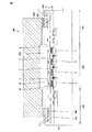
シミュレーションに当たっては、図12に示すようなモデルを想定した。半導体基板1に凹部5を設け、半導体基板1の上側には、半導体基板1に近い側から順に、シリコン酸化膜21、SiN膜22、TEOS膜23、絶縁層27が積層され、さらにその上に最表層としてTEOS膜35が形成されているものとした。絶縁層27はBPSG層によって形成するものとした。絶縁層27に覆われた内部に、サーモパイルに相当するものとして、P型ポリシリコン膜25およびN型ポリシリコン膜26を配置した。凹部5の上方にセンサ部に相当するものとして、サーモパイルを含む部分が浮くように配置されている。TEOS膜35の厚みを調整することによって、センサ部の合計厚みが2.5μmとなるモデルと、4.0μmとなるモデルとの2通りを用意した。これら2通りのモデルに対して、上面から125.94W/m2の熱流束を印加した場合の温度の変遷についてシミュレーションを行なった。
In the simulation, a model as shown in FIG. 12 was assumed. A
シミュレーション結果を図13および図14に示す。センサ部の厚みが2.5μmの場合の結果を図13に示す。発明者らは、温度が最大値の63%に達するまでの時間に注目した。センサ部の厚みが2.5μmの場合、図13から読み取れるように、温度が最大値の63%に達するまでの時間は10ミリ秒であった。 The simulation results are shown in FIG. 13 and FIG. The results when the thickness of the sensor part is 2.5 μm are shown in FIG. The inventors paid attention to the time until the temperature reaches 63% of the maximum value. When the thickness of the sensor portion was 2.5 μm, as can be seen from FIG. 13, the time until the temperature reached 63% of the maximum value was 10 milliseconds.
センサ部の厚みが4.0μmの場合の結果を図14に示す。センサ部の厚みが4.0μmの場合、図14から読み取れるように、温度が最大値の63%に達するまでの時間は13ミリ秒であった。センサ部の厚みが4.0μmの場合に比べて2.5μmの場合は、温度が最大値の63%に達するまでの時間は約0.76倍に短縮されており、応答速度が速くなっているといえる。シミュレーション結果と実測値とでは数値自体には差があるが、おおまかな傾向は合っていると考えられるので、このシミュレーション結果から、センサ部を薄くすることがセンサの高速化に寄与することがわかった。 FIG. 14 shows the result when the thickness of the sensor part is 4.0 μm. When the thickness of the sensor part was 4.0 μm, as can be seen from FIG. 14, the time until the temperature reached 63% of the maximum value was 13 milliseconds. When the thickness of the sensor part is 2.5 μm compared to 4.0 μm, the time until the temperature reaches 63% of the maximum value is shortened by about 0.76 times, and the response speed is increased. It can be said that. Although there is a difference in the numerical value itself between the simulation result and the actual measurement value, it is thought that the general tendency is the same. From this simulation result, it is clear that thinning the sensor part contributes to speeding up the sensor. It was.
なお、今回開示した上記実施の形態はすべての点で例示であって制限的なものではない。本発明の範囲は上記した説明ではなくて特許請求の範囲によって示され、特許請求の範囲と均等の意味および範囲内でのすべての変更を含むものである。 In addition, the said embodiment disclosed this time is an illustration in all the points, Comprising: It is not restrictive. The scope of the present invention is defined by the terms of the claims, rather than the description above, and includes all modifications within the scope and meaning equivalent to the terms of the claims.
1 半導体基板、2 センサ部、2u (センサ部の)上面、5 凹部、21 シリコン酸化膜、22,32 SiN膜、23,31 SiO2膜、24 サーモパイル、25 P型ポリシリコン膜、26 N型ポリシリコン膜、27,30 絶縁層、28a,28b トランジスタ、29a,29b 配線層、33 凹部、34 吸収層、35 TEOS膜、36 凹部、37 金属膜、38 エッチングホール、39 抵抗体、40 配線保護膜、41 上部層、41u (上部層の)上面、101 赤外線センサ、401 センサ領域、402 周辺回路領域、502 キャップ部材、503 封止材、505 内部空間、601 赤外線センサチップ。
1 semiconductor substrate, 2 a sensor unit, 2u (sensor section) top, 5
Claims (4)
前記サーモパイル支持層の上面にサーモパイルを形成する工程と、
前記サーモパイルを形成する工程より後で、前記第2領域に回路素子を形成する工程と、
前記第1領域および前記第2領域を覆って上部層を形成する工程と、
前記第1領域において前記上部層を途中まで掘り下げる工程と、
前記上部層を途中まで掘り下げた領域のうち一部の領域において前記上部層をさらに掘り下げることによって前記半導体基板が露出するエッチングホールを形成する工程と、
前記エッチングホールを通じて前記第1領域にある前記半導体基板の一部をエッチングして前記サーモパイル支持層および前記サーモパイルを前記半導体基板から浮かせることによって、センサ部を形成する工程とを含み、
前記センサ部の上面は、前記第2領域における前記上部層の上面より低い位置となっている、赤外線センサの製造方法。 Forming a thermopile support layer in the first region of the semiconductor substrate having a first region to be a sensor region and a second region to be a peripheral circuit region on the upper surface;
Forming a thermopile on the top surface of the thermopile support layer;
A step of forming a circuit element in the second region after the step of forming the thermopile;
Forming an upper layer covering the first region and the second region;
Digging the upper layer partway in the first region;
Forming an etching hole in which the semiconductor substrate is exposed by further digging down the upper layer in a part of the region where the upper layer is dug down partway;
Forming a sensor part by etching a part of the semiconductor substrate in the first region through the etching hole to float the thermopile support layer and the thermopile from the semiconductor substrate,
The method for manufacturing an infrared sensor, wherein an upper surface of the sensor unit is positioned lower than an upper surface of the upper layer in the second region.
前記半導体基板の上側に形成され、前記凹部に対応した開口部であるセンサ開口部を有する上部層と、
前記センサ開口部の内周の少なくとも1ヶ所につながるように、前記凹部の内面から離隔した状態で前記センサ開口部内に支持されるセンサ部とを備え、
前記センサ部はサーモパイルを備え、
平面的に見て前記センサ開口部とは異なる場所において、回路素子が前記上部層の内部に形成されている周辺回路領域が設けられており、
前記センサ部の上面は、前記周辺回路領域における前記上部層の上面より低い位置にある、赤外線センサ。 A semiconductor substrate having a recess on the upper surface;
An upper layer formed above the semiconductor substrate and having a sensor opening which is an opening corresponding to the recess;
A sensor portion supported in the sensor opening in a state separated from the inner surface of the recess so as to be connected to at least one location on the inner periphery of the sensor opening;
The sensor unit includes a thermopile,
In a place different from the sensor opening in plan view, a peripheral circuit region in which circuit elements are formed inside the upper layer is provided,
An infrared sensor, wherein an upper surface of the sensor unit is positioned lower than an upper surface of the upper layer in the peripheral circuit region.
Priority Applications (3)
| Application Number | Priority Date | Filing Date | Title |
|---|---|---|---|
| JP2013051506A JP2014178172A (en) | 2013-03-14 | 2013-03-14 | Infrared sensor and manufacturing method thereof |
| CN201480010005.0A CN105008877B (en) | 2013-03-14 | 2014-02-18 | Infrared ray sensor and its manufacture method |
| PCT/JP2014/053724 WO2014141823A1 (en) | 2013-03-14 | 2014-02-18 | Infrared sensor and method for manufacturing same |
Applications Claiming Priority (1)
| Application Number | Priority Date | Filing Date | Title |
|---|---|---|---|
| JP2013051506A JP2014178172A (en) | 2013-03-14 | 2013-03-14 | Infrared sensor and manufacturing method thereof |
Publications (1)
| Publication Number | Publication Date |
|---|---|
| JP2014178172A true JP2014178172A (en) | 2014-09-25 |
Family
ID=51536498
Family Applications (1)
| Application Number | Title | Priority Date | Filing Date |
|---|---|---|---|
| JP2013051506A Pending JP2014178172A (en) | 2013-03-14 | 2013-03-14 | Infrared sensor and manufacturing method thereof |
Country Status (3)
| Country | Link |
|---|---|
| JP (1) | JP2014178172A (en) |
| CN (1) | CN105008877B (en) |
| WO (1) | WO2014141823A1 (en) |
Cited By (2)
| Publication number | Priority date | Publication date | Assignee | Title |
|---|---|---|---|---|
| CN108540640A (en) * | 2018-02-12 | 2018-09-14 | 维沃移动通信有限公司 | A kind of determination method, apparatus of infrared detecting device, mobile terminal and infrared remote receiver |
| CN112591706A (en) * | 2020-12-03 | 2021-04-02 | 杭州士兰集昕微电子有限公司 | Thermopile sensor system for integrated CMOS circuits and method of fabrication |
Citations (3)
| Publication number | Priority date | Publication date | Assignee | Title |
|---|---|---|---|---|
| WO2010035739A1 (en) * | 2008-09-25 | 2010-04-01 | パナソニック電工株式会社 | Infrared sensor |
| JP2011179953A (en) * | 2010-03-01 | 2011-09-15 | Rohm Co Ltd | Infrared sensor |
| JP2012083341A (en) * | 2010-09-13 | 2012-04-26 | Ricoh Co Ltd | Thermal-type infrared-ray sensor and method of manufacturing the same |
Family Cites Families (8)
| Publication number | Priority date | Publication date | Assignee | Title |
|---|---|---|---|---|
| US6828172B2 (en) * | 2002-02-04 | 2004-12-07 | Delphi Technologies, Inc. | Process for a monolithically-integrated micromachined sensor and circuit |
| CN1692504A (en) * | 2002-12-05 | 2005-11-02 | 松下电器产业株式会社 | Pyroelectric device, method for manufacturing same and infrared sensor |
| JP4086875B2 (en) * | 2003-09-09 | 2008-05-14 | 旭化成エレクトロニクス株式会社 | Infrared sensor IC, infrared sensor and manufacturing method thereof |
| JP2005241457A (en) * | 2004-02-26 | 2005-09-08 | Hamamatsu Photonics Kk | Infrared sensor, and manufacturing method therefor |
| JP5079211B2 (en) * | 2004-10-13 | 2012-11-21 | 浜松ホトニクス株式会社 | Infrared detector and manufacturing method thereof |
| JP4661207B2 (en) * | 2004-12-20 | 2011-03-30 | 日産自動車株式会社 | Infrared sensor manufacturing method |
| JP2009174917A (en) * | 2008-01-22 | 2009-08-06 | Oki Semiconductor Co Ltd | Infrared detection element and manufacturing method for infrared detection element |
| JP2011232261A (en) * | 2010-04-28 | 2011-11-17 | Shimadzu Corp | Thermal type infrared-ray sensor |
-
2013
- 2013-03-14 JP JP2013051506A patent/JP2014178172A/en active Pending
-
2014
- 2014-02-18 WO PCT/JP2014/053724 patent/WO2014141823A1/en active Application Filing
- 2014-02-18 CN CN201480010005.0A patent/CN105008877B/en active Active
Patent Citations (3)
| Publication number | Priority date | Publication date | Assignee | Title |
|---|---|---|---|---|
| WO2010035739A1 (en) * | 2008-09-25 | 2010-04-01 | パナソニック電工株式会社 | Infrared sensor |
| JP2011179953A (en) * | 2010-03-01 | 2011-09-15 | Rohm Co Ltd | Infrared sensor |
| JP2012083341A (en) * | 2010-09-13 | 2012-04-26 | Ricoh Co Ltd | Thermal-type infrared-ray sensor and method of manufacturing the same |
Cited By (3)
| Publication number | Priority date | Publication date | Assignee | Title |
|---|---|---|---|---|
| CN108540640A (en) * | 2018-02-12 | 2018-09-14 | 维沃移动通信有限公司 | A kind of determination method, apparatus of infrared detecting device, mobile terminal and infrared remote receiver |
| CN112591706A (en) * | 2020-12-03 | 2021-04-02 | 杭州士兰集昕微电子有限公司 | Thermopile sensor system for integrated CMOS circuits and method of fabrication |
| CN112591706B (en) * | 2020-12-03 | 2024-02-23 | 杭州士兰集昕微电子有限公司 | Thermopile sensor system of integrated CMOS circuit and manufacturing method thereof |
Also Published As
| Publication number | Publication date |
|---|---|
| CN105008877A (en) | 2015-10-28 |
| WO2014141823A1 (en) | 2014-09-18 |
| CN105008877B (en) | 2017-03-08 |
Similar Documents
| Publication | Publication Date | Title |
|---|---|---|
| CN102901567B (en) | Thermopile infrared detector, array and preparation method of thermopile infrared detector | |
| JP4858547B2 (en) | Semiconductor device and manufacturing method thereof | |
| US10158949B2 (en) | MEMS microphone and method of manufacturing the same | |
| JP2012202786A (en) | Thermal type sensor and method for manufacturing the same | |
| JP2012154784A (en) | Electrostatic capacitance type pressure sensor and manufacturing method of electrostatic capacitance type pressure sensor | |
| US9257587B2 (en) | Suspension and absorber structure for bolometer | |
| US7832279B2 (en) | Semiconductor device including a pressure sensor | |
| JP5605347B2 (en) | Manufacturing method of semiconductor device | |
| WO2014141823A1 (en) | Infrared sensor and method for manufacturing same | |
| TWI601686B (en) | Method for manufacturing semiconductor gas sensing device and semiconductor gas sensing device | |
| EP2796844B1 (en) | Mems capacitive pressure sensor | |
| JP2008294229A (en) | Wafer-level package structure and sensor device | |
| WO2016199349A1 (en) | Semiconductor device and method for producing same | |
| JP2007263765A (en) | Wafer level package structure and sensor device | |
| CN109540371B (en) | Pressure sensor and manufacturing method thereof | |
| JP2016051754A (en) | Method of manufacturing semiconductor device | |
| CN103342333A (en) | Infrared thermopile type sensor based on CMOS DPTM process and manufacturing method thereof | |
| JP2013187512A (en) | Semiconductor device | |
| US8853800B2 (en) | Integrated device of the type comprising at least a microfluidic system and further circuitry and corresponding integration process | |
| JP2019054143A (en) | Connection structure and method for manufacturing the same, and sensor | |
| JP2015135306A (en) | Infrared sensor and manufacturing method thereof | |
| US20100229651A1 (en) | Cointegrated mems sensor and method | |
| JP6323278B2 (en) | Semiconductor physical quantity sensor and manufacturing method thereof | |
| JP2011214857A (en) | Infrared sensor element | |
| JP2017212530A (en) | MEMS element |
Legal Events
| Date | Code | Title | Description |
|---|---|---|---|
| A621 | Written request for application examination |
Free format text: JAPANESE INTERMEDIATE CODE: A621 Effective date: 20151106 |
|
| A131 | Notification of reasons for refusal |
Free format text: JAPANESE INTERMEDIATE CODE: A131 Effective date: 20160524 |
|
| A521 | Request for written amendment filed |
Free format text: JAPANESE INTERMEDIATE CODE: A523 Effective date: 20160712 |
|
| A131 | Notification of reasons for refusal |
Free format text: JAPANESE INTERMEDIATE CODE: A131 Effective date: 20161220 |
|
| A02 | Decision of refusal |
Free format text: JAPANESE INTERMEDIATE CODE: A02 Effective date: 20170711 |